EP2130953A2 - Epitaxial silicon wafer and method for producing the same - Google Patents
Epitaxial silicon wafer and method for producing the same Download PDFInfo
- Publication number
- EP2130953A2 EP2130953A2 EP09007408A EP09007408A EP2130953A2 EP 2130953 A2 EP2130953 A2 EP 2130953A2 EP 09007408 A EP09007408 A EP 09007408A EP 09007408 A EP09007408 A EP 09007408A EP 2130953 A2 EP2130953 A2 EP 2130953A2
- Authority
- EP
- European Patent Office
- Prior art keywords
- silicon wafer
- epitaxial
- wafer
- epitaxial film
- silicon
- Prior art date
- Legal status (The legal status is an assumption and is not a legal conclusion. Google has not performed a legal analysis and makes no representation as to the accuracy of the status listed.)
- Withdrawn
Links
Images



Classifications
-
- C—CHEMISTRY; METALLURGY
- C30—CRYSTAL GROWTH
- C30B—SINGLE-CRYSTAL GROWTH; UNIDIRECTIONAL SOLIDIFICATION OF EUTECTIC MATERIAL OR UNIDIRECTIONAL DEMIXING OF EUTECTOID MATERIAL; REFINING BY ZONE-MELTING OF MATERIAL; PRODUCTION OF A HOMOGENEOUS POLYCRYSTALLINE MATERIAL WITH DEFINED STRUCTURE; SINGLE CRYSTALS OR HOMOGENEOUS POLYCRYSTALLINE MATERIAL WITH DEFINED STRUCTURE; AFTER-TREATMENT OF SINGLE CRYSTALS OR A HOMOGENEOUS POLYCRYSTALLINE MATERIAL WITH DEFINED STRUCTURE; APPARATUS THEREFOR
- C30B29/00—Single crystals or homogeneous polycrystalline material with defined structure characterised by the material or by their shape
- C30B29/02—Elements
- C30B29/06—Silicon
-
- H—ELECTRICITY
- H10—SEMICONDUCTOR DEVICES; ELECTRIC SOLID-STATE DEVICES NOT OTHERWISE PROVIDED FOR
- H10P—GENERIC PROCESSES OR APPARATUS FOR THE MANUFACTURE OR TREATMENT OF DEVICES COVERED BY CLASS H10
- H10P14/00—Formation of materials, e.g. in the shape of layers or pillars
- H10P14/20—Formation of materials, e.g. in the shape of layers or pillars of semiconductor materials
-
- C—CHEMISTRY; METALLURGY
- C30—CRYSTAL GROWTH
- C30B—SINGLE-CRYSTAL GROWTH; UNIDIRECTIONAL SOLIDIFICATION OF EUTECTIC MATERIAL OR UNIDIRECTIONAL DEMIXING OF EUTECTOID MATERIAL; REFINING BY ZONE-MELTING OF MATERIAL; PRODUCTION OF A HOMOGENEOUS POLYCRYSTALLINE MATERIAL WITH DEFINED STRUCTURE; SINGLE CRYSTALS OR HOMOGENEOUS POLYCRYSTALLINE MATERIAL WITH DEFINED STRUCTURE; AFTER-TREATMENT OF SINGLE CRYSTALS OR A HOMOGENEOUS POLYCRYSTALLINE MATERIAL WITH DEFINED STRUCTURE; APPARATUS THEREFOR
- C30B15/00—Single-crystal growth by pulling from a melt, e.g. Czochralski method
- C30B15/02—Single-crystal growth by pulling from a melt, e.g. Czochralski method adding crystallising materials or reactants forming it in situ to the melt
-
- C—CHEMISTRY; METALLURGY
- C30—CRYSTAL GROWTH
- C30B—SINGLE-CRYSTAL GROWTH; UNIDIRECTIONAL SOLIDIFICATION OF EUTECTIC MATERIAL OR UNIDIRECTIONAL DEMIXING OF EUTECTOID MATERIAL; REFINING BY ZONE-MELTING OF MATERIAL; PRODUCTION OF A HOMOGENEOUS POLYCRYSTALLINE MATERIAL WITH DEFINED STRUCTURE; SINGLE CRYSTALS OR HOMOGENEOUS POLYCRYSTALLINE MATERIAL WITH DEFINED STRUCTURE; AFTER-TREATMENT OF SINGLE CRYSTALS OR A HOMOGENEOUS POLYCRYSTALLINE MATERIAL WITH DEFINED STRUCTURE; APPARATUS THEREFOR
- C30B25/00—Single-crystal growth by chemical reaction of reactive gases, e.g. chemical vapour-deposition growth
- C30B25/02—Epitaxial-layer growth
-
- H—ELECTRICITY
- H10—SEMICONDUCTOR DEVICES; ELECTRIC SOLID-STATE DEVICES NOT OTHERWISE PROVIDED FOR
- H10P—GENERIC PROCESSES OR APPARATUS FOR THE MANUFACTURE OR TREATMENT OF DEVICES COVERED BY CLASS H10
- H10P36/00—Gettering within semiconductor bodies
-
- Y—GENERAL TAGGING OF NEW TECHNOLOGICAL DEVELOPMENTS; GENERAL TAGGING OF CROSS-SECTIONAL TECHNOLOGIES SPANNING OVER SEVERAL SECTIONS OF THE IPC; TECHNICAL SUBJECTS COVERED BY FORMER USPC CROSS-REFERENCE ART COLLECTIONS [XRACs] AND DIGESTS
- Y10—TECHNICAL SUBJECTS COVERED BY FORMER USPC
- Y10T—TECHNICAL SUBJECTS COVERED BY FORMER US CLASSIFICATION
- Y10T428/00—Stock material or miscellaneous articles
- Y10T428/21—Circular sheet or circular blank
Definitions
- the present invention relates to an epitaxial silicon wafer having an epitaxial film only on the front side (one side) and a method for producing the epitaxial silicon wafer.
- Silicon wafers are produced in various steps at which first a single crystal ingot (silicon single crystal) is pulled up by the CZ (Czochralski) method and the ingot is subjected to slicing, beveling, lapping, etching, mirror polishing and washing, for example.
- CZ Czochralski
- COP-frec crystal defectless crystal
- Patent Document 1 Japanese Unexamined Patent Publication No. H06-112120
- Patent Document 1 Japanese Unexamined Patent Publication No. H06-112120
- an epitaxial silicon wafer will have the following problems. More specifically, since atoms forming the bulk wafer are different in lattice constant from atoms forming the epitaxial film, it is more likely that the silicon wafer and also the epitaxial silicon wafer will warp. These wafers will warp more greatly as they are increased in size (Patent Document 1).
- a silicon wafer adopted is, for example, a wafer obtained from a highly resistant boron-doped single crystal ingot (0.1 ⁇ cm or more in specific resistance) in which the boron concentration is less than 2.7 ⁇ 10 17 atoms/cm 3 .
- the epitaxial film is grown on a wafer lower in boron concentration, a dopant is dispersed outwardly from the back side of the wafer, thus suppressing the occurrence of auto-doping phenomena where the dopant penetrates the epitaxial film on a device forming face.
- boron inside the wafer becomes a seed growth of intrinsic gettering (IC).
- IC intrinsic gettering
- the inventor has found that in production of an epitaxial silicon wafer, some intrinsic gettering functions may be imparted to a silicon wafer which is 450 mm or more in diameter and 0.1 ⁇ cm or more (high resistance) in specific resistance.
- the inventor has also found that even a wafer, the one side of which is epitaxially grown, is less likely to warp greatly and provided with a high intrinsic gettering performance and has thus accomplished the present invention.
- An object of the present invention is to provide an epitaxial silicon wafer in which on growing an epitaxial film only on the front side of a large-sized wafer which is 450 mm or more in diameter, the wafer can be decreased in warpage to obtain a high intrinsic guttering performance and a method for producing the epitaxial silicon wafer.
- the invention described in claim 1 is an epitaxial silicon wafer in which an epitaxial film is grown only on the front side of a silicon wafer obtained by processing a silicon single crystal pulled up by the CZ method which is 450 mm or more in diameter and 0.1 ⁇ cm or more in specific resistance, and the epitaxial silicon wafer in which the silicon wafer has intrinsic gettering functions.
- intrinsic gettering functions arc imparted to a silicon wafer at a high resistance of 0.1 ⁇ cm or more in specific resistance and 450 mm or more in diameter, thereby even a large-sized wafer which is 450 mm or more in diameter is less likely to warp greatly after the growth of an epitaxial film and is able to obtain a high intrinsic gettering performance.
- the silicon wafer may be available in any size, as long as the diameter is 450 mm or more.
- Single crystal silicon which is the same as the wafer may be adopted as a material of the opitaxial film.
- a material different from the wafer for example, gallium or arsenic.
- the thickness of the epitaxial film is, for example, from several ⁇ m to 150 ⁇ m for high polar devices or power devices and 10 ⁇ m or less for MOS devices.
- any epitaxial method may be adopted, for example, a vapor phase epitaxial method, a liquid phase epitaxial method or a solid phase epitaxial method.
- the vapor phase epitaxial method includes, for example, a normal-pressure vapor phase epitaxial method, a reduced-pressure vapor phase epitaxial method and an organic-metal vapor phase epitaxial method.
- an opitaxial silicon wafer is kept horizontal (with the front side and the back side kept parallel to each other) and accommodated at a wafer accommodating part. Used is a susceptor which is circular in a planar view and able to place one sheet of the wafer.
- the vapor phase epitaxial method may include homoepitaxy in which the same material as a silicon wafer is epitaxially grown and heteroepitaxy in which a material different from the wafer such as (GaAs) is epitaxially grown.
- a vapor phase epitaxial growth apparatus may be structured in any way as long as it is a one-side vapor phase epitaxial growth apparatus in which an epitaxial film can be grown only on one side of a silicon wafer.
- the vapor phase epitaxial growth apparatus may include a sheet type, or a pancake type, a barrel type, a hot-wall type and a cluster type capable of processing a plurality of silicon wafers at the same time.
- a method for imparting intrinsic gettering functions to a silicon wafer includes, for example, doping of a nitrogen element in a range of 1 ⁇ 10 13 to 1 ⁇ 10 15 atoms/cm 3 to a melt (silicon) and doping of a carbon element in a range of 1 ⁇ 10 15 to 1 ⁇ 10 17 atoms/cm 3 to a melt.
- the invention described in claim 2 is the cpitaxial silicon wafer of claim 1 in which the silicon wafer contains at least one of a nitrogen element in a range of 1 ⁇ 10 13 to 1 ⁇ 10 15 atoms/cm 3 and a carbon element in a range of 1 ⁇ 10 15 to 1 ⁇ 10 17 atoms/cm 3 .
- a silicon wafer contains any one of a nitrogen element in a range of 1 ⁇ 10 13 to 1 ⁇ 10 15 atoms/cm 3 , a carbon element in a range of 1 ⁇ 10 15 to 1 ⁇ 10 17 atoms/cm 3 and both the nitrogen element and Lhe carbon element.
- the wafer is less likely to warp greatly after the growth of an epitaxial film.
- it is possible to decrease the warpage of the wafer and also obtain a high intrinsic gettering performance.
- the invention described in claim 3 is a method for producing an epitaxial silicon wafer in which an epitaxial film is grown only on the front side of a silicon wafer obtained from a silicon single crystal pulled up from a melt inside a crucible by the CZ method which is 0.1 ⁇ cm or more in specific resistance and 450 mm or more in diame ter, and the method for producing the epitaxial silicon wafer in which intrinsic gettering functions are imparted to the silicon wafer by doping at least one of (1) a nitrogen element in a range of 1 ⁇ 10 13 to 1 ⁇ 10 15 atoms/cm 3 to the melt and (2) a carbon element in a range of 1 ⁇ 10 15 to 1 ⁇ 10 17 atoms/cm 3 to the melt.
- intrinsic gettering functions are imparted to a high resistance large-sized silicon wafer which is 450 mm or more in diameter and 0.1 ⁇ cm or more in specific resistance. More specifically, performed is at least one of doping of a nitrogen element in a range of 1 ⁇ 10 13 to 1 ⁇ 10 15 atoms/cm 3 to a silicon melt, doping of a carbon clement in a range of 1 ⁇ 10 15 to 1 ⁇ 10 17 atoms/cm 3 to the melt and doping of both the nitrogen element and the carbon element.
- the wafer is less likely to warp greatly after the growth of the epitaxial film. As a result, it is possible to decrease the warpage of the wafer and obtain a high intrinsic gettering performance.
- a method for increasing the specific resistance of a silicon wafer adopted is a method for adding a dopant such as boron or phosphorus to a silicon melt in a crucible when an ingot is pulled up.
- a dopant such as boron or phosphorus
- Other dopants such as arsenic and antimony may be added.
- the invention described in claim 4 is the method for producing the epitaxial silicon wafer described in claim 3 in which after growth of the epitaxial film, the front side of the epitaxial film and the back side of the silicon wafer are polished at the same time.
- the front side of the epitaxial film and the back side of the silicon wafer are polished at the same time, by which both sides of the epitaxial silicon wafer can be increased in planarization. It is also possible to reduce the time necessary in the step of polishing the epitaxial film on both sides of the wafer and to increase the productivity.
- a method for polishing both the front side and the back side of an epitaxial silicon wafer adopted is a sheet-type double side polishing method in which an epitaxial silicon wafer is polished on the front side and the back side at the same time between a lower surface plate having a polishing cloth stretched out on the upper face and an upper surface plate having a polishing cloth stretched out on the lower face. Further, there may be adopted a double side polishing method in which no sun gear is used and a carrier plate having an epitaxial silicon wafer accommodated at a wafer retaining hole is allowed to perform circular movements not in conjunction with rotation on its own axis between a polishing cloth-equipped lower surface plate and a polishing cloth-equipped upper surface plate.
- intrinsic gettering functions are imparted to a large-sized and high-resistant silicon wafer which is 450 mm or more in diameter and 0.1 ⁇ cm or more in specific resistance, thereby the wafer is less likely to warp greatly after the growth of an epitaxial film. As a result, it is possible to decrease the warpage of the epitaxial silicon wafer and also obtain a high intrinsic gettering performance.
- the front side of the epitaxial film and the back side of the silicon wafer are polished at the same time.
- the epitaxial silicon wafer can be increased in planarization on both sides, and also the time necessary in the step of polishing the epitaxial film on both sides of the wafer can be reduced to increase the productivity.
- the numcral 10 depicts an epitaxial silicon wafer of the example 1 in the present invention.
- the epitaxial silicon wafer 10 is based on a silicon wafer 11 which is obtained by processing a silicon single crystal pulled up by the CZ method so as to be 450 mm in diameter and 1.0 ⁇ cm in specific resistance by boron dope.
- the epitaxial silicon wafer 10 is a two-layer structured wafer of which an epitaxial film 12 made up of single crystal silicon is grown by a vapor phase epitaxial method only on the front side of the silicon wafer 11.
- a nitrogen element is doped in a range of 1 ⁇ 10 14 atoms/cm 3 to the silicon wafer 11.
- the silicon wafer 11 is produced in steps at which a single crystal silicon ingot is pulled up by the CZ method from a silicon melt to which horon is doped at a predetermined amount inside a crucible (S100), thereafter, the ingot is sliced into many wafers (S101), each of the wafers is subsequently subjected to beveling (S102), lapping (S103), etching (S 104) and double side polishing (S105).
- the epitaxial film 12 is grown on the front side of the silicon wafer 11 by a vapor phase epitaxial method (S106). Thereafter, the front side of the epitaxial film 12 and the back side of the silicon wafer 11 are polished at the same time (S107). Thereby, produced is the epitaxial silicon wafer 10 (S108).
- a crystal growth apparatus shown in Figure 3 is used to grow a silicon single crystal.
- the thus produced silicon single crystal is 470 mm in diameter at the trunk part thereof which is sufficient in forming a 450 mm-sized silicon wafer.
- the number 40 depicts a silicon single crystal growth apparatus (hereinafter referred to as a crystal growth apparatus) used in the example 1 of the present invention.
- the crystal growth apparatus 40 is provided with a chamber 41 formed in a hollow cylindrical shape.
- the chamber 41 is made up of a main chamber 42 and a pull chamber 43 which is continuously fixed on the main chamber 42 and smaller in diameter than the main chamber 42.
- a crucible 44 is fixed on a supporting shaft 45 (pedestal) which can rotate and move up and down freely.
- the crucible 44 has a double structure in combination with a quartz crucible 46 on the inside with a graphite crucible 47 on the outside.
- a thermal resistance type heater 51 is arranged outside the crucible 44 so as to be concentric with respect to the wall of the crucible 44.
- a cylindrical thermal insulalion tube 52 is arranged outside the heater 51 along the inner face of the circumferential wall of the main chamber 42.
- a circular thermal insulation plate 53 is arranged on the bottom face of the main chamber 42.
- a pulling-up shaft 55 capable of rotating and moving up and down on the same shaft with respect to the supporting shaft 45 (a wire will do) is hung through the pull chamber 43 on the center line of the crucible 44.
- a seed crystal C is loaded at the lower end of the pulling-up shaft 55.
- a silicon raw material for crystallization and boron for an impurity are fed into the crucible 44 so as to give 1.0 ⁇ cm in specific resistance of the silicon single crystal S.
- Pressure inside the chamber 41 is reduced to 25 Torr, and argon gas which contains nitrogen gas in 100 L/min is introduced thereinto.
- a resultant inside the crucible 44 is dissolved by the heater 51 to form a melt 56 inside the crucible 44.
- the seed crystal C loaded at the lower end of the pulling up shaft 55 is submerged into the melt 56, and the pulling-up shaft 55 is pulled up axially while the crucible 44 and the pulling-up shaft 55 are allowed to rotate in the reverse direction with respect to one another, thus growing the silicon single crystal S below the seed crystal C.
- a silicon single crystal (ingot) S which is 1 ⁇ 10 14 atoms/cm 3 in nitrogen element and 1.0 ⁇ cm in specific resistance by boron dope.
- a wire saw in which a wire is wound around three group rollers arranged in a triangular shape when viewed from the side is used.
- the wire saw slices many silicon wafers 11 from the silicon single crystal S.
- a beveling grind stone in rotation is pressed against an outer circumference of the silicon wafer 11 to effect beveling.
- the lapping step (S103) a double side lapping machine is used to lap both sides of the silicon wafer 11 at the same time. More specifically, both sides nf the silicon wafer 11 are lapped between the upper and the lower surface plates rotating at a predetermined speed.
- the silicon wafer 11 after lapping is submerged into an acid etching solution pooled in an etching tank to effect etching, thereby removing damage resulting from the beveling and the lapping.
- a double side polishing machine free of a sun gear is used to mirror-polish the both sides of the silicon wafer 11 at the same time.
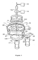
- a description will be given specifically for a structure of the double side polishing machine structured so as to be free of a sun gear by referring to Figure 4 and Figure 5 .
- an upper surface plate 120 is rotated and driven within a horizontal plane via a rotating shaft 12a extending upward by an upper-side rotating motor 16. Further, the upper surface plate 120 is caused to vertically move up and down by an elevating machine 18 moving back and forth axially.
- the elevating machine 18 is used when the epitaxial silicon wafer 11 is fed to and discharged from the carrier plate 110.
- both the front and back sides of the epitaxial silicon wafer 11 on the upper surface plate 120 and the lower surface plate 130 are pressed by pressure means such as airbag-type means (not illustrated) assembled into the upper surface plate 120 and the lower surface plate 130.
- the lower surface plate 130 is rotated via the output shaft 17a thereof within a horizontal plane by a lower-side rotating motor 17.
- the carrier plate 110 moves circularly within a face (horizontal plane) parallel with the surface of the plate 110 by a carrier circular movement mechanism 19 so that the plate 110 itself will not rotate on its own axis.
- the carrier circular movement mechanism 19 is provided with an annular carrier holder 20 for holding the carrier plate 110 from outside.
- the carrier circular movement mechanism 19 is connected to the carrier holder 20 via a connecting structure.
- Four bearing units 20b projected outward at every 90 degrees are placed on an outer circumference of the carrier holder 20.
- An eccentric shaft 24a installed in a projecting manner at an eccentric position of the upper face of an eccentric arm 24 formed in a small-sized circular disk shape is inserted into each of the bearing units 20b.
- a rotating shaft 24b is installed vertically at the center of the lower face of each of these four occentric arms 24.
- These rotating shafts 24b are inserted into four bearing units 25a which are placed at every 90 degrees on an annular base 25, with the respective leading ends projected downward.
- Sprockets 26 are firmly fixed to the respective leading ends of the rotating shafts 24b projected below.
- a timing chain 27 is hung over on cach of the sprockets 26 continuously in a horizontal state. These four sprockets 26 and the timing chain 27 cause the four rotating shafts 24b to rotate at the same time so that the four eccentric arms 24 move circularly in synchronization.
- the rotating shafts 24b Of these four rotating shafts 24b, one of them is formed in a longer shape, and the leading end thereof projects further below than the sprocket 26, at which a gear 28 for power transmission is firmly fixed.
- the gear 28 is meshed with a large-sized driving gear 30 firmly fixed on an output shaft of a circular movement motor 29 extending upward. Therefore, on actuation of the circular movement motor 29, the rotating force thereof will be transmitted to the timing chain 27 via the gears 30, 28 and the sprocket 26 firmly fixed to the longer rotating shaft 24b.
- the timing chain 27 rotates circumferentially, by which the four eccentric arms 24 rotate at the center of the rotating shaft 24b within a horizontal plane in synchronization via the other three sprockets 26.
- the carrier holder 20 connected together with each of the eccentric shafts 24a and a carrier plate 110 held by the holder 20 perform circular movements without rotation on its own axis within a horizontal plane parallel with the plate 110. More specifically, the carrier plate 110 rotates, with such a state kept that it is eccentric only by a distance L from an axis line e between the upper surface plate 120 and the lower surface plate 130.
- the polishing cloth 15 is stretched out on each face opposing the surface plates 120, 130.
- the distance L is equal to a distance between the eccentric shaft 24a and the rotating shaft 24b.
- the circular movements without rotation on its own axis allow all points on the carrier plate 110 to exhibit a small-circular locus equal in dimension.
- the silicon wafer 11 accommodated at a wafer accommodating portion 11a formed on the carrier plate 110 is polished on the both sides.
- the vapor phase epitaxial growth apparatus 60 is that in which a susceptor 61 which is circular in a planar view and capable of placing one sheet of a silicon wafer 11 is placed horizontally at the center of a chamber having a heater at the upper and the lower parts thereof.
- the susceptor 61 is fabricated by coating a carbon-made base material with SiC.
- a recessed counterbore (wafer accommodating portion) 62 which accommodates the silicon wafer 11 in a horizontally kept state (a state in which the front side and the back side are in a horizontal position) is formed at an inner circumference on the upper face of the susceptor 61.
- the counterbore 62 is made up of a circumferential wall 62a, a 6 mm-wide step 62b which is annular in a planar view and a bottom plate (bottom wall face of the counterbore) 62c.
- a gas supply port which allows a predetermined carrier gas (H 2 gas) and predetermined source gas (SiHCl 3 gas) to flow parallel with the front side of the wafer at an upper space hollow of the chamber is placed at one side portion of the chamber. Further, a gas discharge port is formed on the other side portion of the chamber.
- the silicon wafer 11 is laid laterally on the counterbore 62, with the front side and the back side of a wafer kept horizontal.
- an epitaxial film 12 is grown on the front side of the silicon wafer 11. More specifically, the carrier gas and the source gas are introduced into a reaction chamber through corresponding gas supply ports. The pressure inside the chamber is kept at 100 ⁇ 20 KPa and silicon formed by thermal decomposition or reduction of the source gas is deposited at the reaction speed of 3.5 to 4.5 ⁇ m/minute on the silicon wafer 11 heated at high temperatures of 1000°C to 1150°C. Thereby, the epitaxial film 12 which is approximately 10 ⁇ m in thickness of the silicon single crystal is formed on the front side of the silicon wafer 11. Thus, produced is the epitaxial silicon wafer 10.
- a double side polishing machine structured so as to be free of a sun gear which is used in the double side polishing sep (S105) is used to mirror-polish the front side of the epitaxial film 12 and the back side of the silicon wafer 11 at the same time.
- S105 double side polishing machine structured so as to be free of a sun gear which is used in the double side polishing sep
- the epitaxial film 12 is grown on the silicon wafer 11 lower in boron concentration, a dopant is dispersed outwardly from the back side of the wafer, thus suppressing the occurrence of auto-doping phenomena where the dopant penetrates the epitaxial film 12 on which a device is formed.
- a nitrogen element at 1 ⁇ 10 14 atoms/cm 3 has been doped to the silicon wafer 11.
- the silicon wafer 11 is a high resistant wafer lower in boron concentration, it is provided with a high intrinsic gette ring performance.
- a double side polishing machine structured so as to be free of a sun gear is used to polish the front side of the epitaxial film 12 and the back side of the silicon wafer 11 at the same time.
- the epitaxial silicon wafer 10 can be increased in planarization. Further, the time necessary for the polishing can be reduced to increase the productivity.
- the front side of the epitaxial film 12 and the back side of the silicon wafer 11 are not polished at the same time but may be polished by one side separately.
- a method for imparting intrinsic gettering functions to the silicon wafer 11 there is adopted a method in which the nitrogen element at 1 ⁇ 10 14 atoms/cm 3 is doped to the melt 56.
- carbon powder may be added so as to give 1 ⁇ 10 17 atoms/cm 3 to the melt 56.
- both the nitrogen dope and the carbon dope may be performed.
Landscapes
- Chemical & Material Sciences (AREA)
- Engineering & Computer Science (AREA)
- Crystallography & Structural Chemistry (AREA)
- Materials Engineering (AREA)
- Metallurgy (AREA)
- Organic Chemistry (AREA)
- Chemical Kinetics & Catalysis (AREA)
- General Chemical & Material Sciences (AREA)
- Crystals, And After-Treatments Of Crystals (AREA)
- Recrystallisation Techniques (AREA)
- Chemical Vapour Deposition (AREA)
Abstract
Description
- The present invention relates to an epitaxial silicon wafer having an epitaxial film only on the front side (one side) and a method for producing the epitaxial silicon wafer.
- Silicon wafers are produced in various steps at which first a single crystal ingot (silicon single crystal) is pulled up by the CZ (Czochralski) method and the ingot is subjected to slicing, beveling, lapping, etching, mirror polishing and washing, for example. However, it is anticipated that as wafers become progressively larger in size, in association with production of the single crystal ingot and silicon wafers, there may be a greater difficulty in producing a defectless crystal (COP-frec crystal) due to technical problems of pulling up the ingot, yields and others.
Therefore, in order to make defectless the front side of a wafer on which a device is formed, hereinafter, such a method will become predominant that the vapor phase epitaxial method disclosed in Patent Document 1 (Japanese Unexamined Patent Publication No.H06-112120 - However, where a bulk wafer (silicon wafer) is different in material from an epitaxial film or where a dopant contained in the bulk wafer is different in concentraton from that contained in the epitaxial film, an epitaxial silicon wafer will have the following problems. More specifically, since atoms forming the bulk wafer are different in lattice constant from atoms forming the epitaxial film, it is more likely that the silicon wafer and also the epitaxial silicon wafer will warp. These wafers will warp more greatly as they are increased in size (Patent Document 1).
- Therefore, there is presented an idea that, as a silicon wafer adopted is, for example, a wafer obtained from a highly resistant boron-doped single crystal ingot (0.1 Ω·cm or more in specific resistance) in which the boron concentration is less than 2.7 × 10¹⁷atoms/cm3. Thereby, stress resulting from a difference in atomic radius between a bulk wafer and an epitaxial film is decreased, and when the epitaxial film is grown on the front side of the water, it is less likely that the wafer warps greatly. Further, since the epitaxial film is grown on a wafer lower in boron concentration, a dopant is dispersed outwardly from the back side of the wafer, thus suppressing the occurrence of auto-doping phenomena where the dopant penetrates the epitaxial film on a device forming face. Still further, it is known that boron inside the wafer becomes a seed growth of intrinsic gettering (IC). However, as compared with a wafer higher in boron concentration, a wafer lower in boron concentration is low in intrinsic gettering performance.
- Thus, as a result of intensive research, the inventor has found that in production of an epitaxial silicon wafer, some intrinsic gettering functions may be imparted to a silicon wafer which is 450 mm or more in diameter and 0.1 Ω·cm or more (high resistance) in specific resistance. The inventor has also found that even a wafer, the one side of which is epitaxially grown, is less likely to warp greatly and provided with a high intrinsic gettering performance and has thus accomplished the present invention.
- An object of the present invention is to provide an epitaxial silicon wafer in which on growing an epitaxial film only on the front side of a large-sized wafer which is 450 mm or more in diameter, the wafer can be decreased in warpage to obtain a high intrinsic guttering performance and a method for producing the epitaxial silicon wafer.
- The invention described in claim 1 is an epitaxial silicon wafer in which an epitaxial film is grown only on the front side of a silicon wafer obtained by processing a silicon single crystal pulled up by the CZ method which is 450 mm or more in diameter and 0.1 Ω·cm or more in specific resistance, and the epitaxial silicon wafer in which the silicon wafer has intrinsic gettering functions.
- According to the invention described in claim 1, intrinsic gettering functions arc imparted to a silicon wafer at a high resistance of 0.1 Ω·cm or more in specific resistance and 450 mm or more in diameter, thereby even a large-sized wafer which is 450 mm or more in diameter is less likely to warp greatly after the growth of an epitaxial film and is able to obtain a high intrinsic gettering performance.
- The silicon wafer may be available in any size, as long as the diameter is 450 mm or more.
Single crystal silicon which is the same as the wafer may be adopted as a material of the opitaxial film. Also, acceptable is a material different from the wafer, for example, gallium or arsenic.
The thickness of the epitaxial film is, for example, from several µm to 150 µm for high polar devices or power devices and 10 µm or less for MOS devices. - Any epitaxial method may be adopted, for example, a vapor phase epitaxial method, a liquid phase epitaxial method or a solid phase epitaxial method. Of these methods, the vapor phase epitaxial method includes, for example, a normal-pressure vapor phase epitaxial method, a reduced-pressure vapor phase epitaxial method and an organic-metal vapor phase epitaxial method. In the vapor phase epitaxial method, for example, an opitaxial silicon wafer is kept horizontal (with the front side and the back side kept parallel to each other) and accommodated at a wafer accommodating part. Used is a susceptor which is circular in a planar view and able to place one sheet of the wafer. The vapor phase epitaxial method may include homoepitaxy in which the same material as a silicon wafer is epitaxially grown and heteroepitaxy in which a material different from the wafer such as (GaAs) is epitaxially grown.
- A vapor phase epitaxial growth apparatus may be structured in any way as long as it is a one-side vapor phase epitaxial growth apparatus in which an epitaxial film can be grown only on one side of a silicon wafer. The vapor phase epitaxial growth apparatus may include a sheet type, or a pancake type, a barrel type, a hot-wall type and a cluster type capable of processing a plurality of silicon wafers at the same time.
A method for imparting intrinsic gettering functions to a silicon wafer includes, for example, doping of a nitrogen element in a range of 1 × 10¹³ to 1 × 10¹⁵ atoms/cm3 to a melt (silicon) and doping of a carbon element in a range of 1 × 10¹⁵ to 1 × 10 17 atoms/cm3 to a melt. - The invention described in claim 2 is the cpitaxial silicon wafer of claim 1 in which the silicon wafer contains at least one of a nitrogen element in a range of 1 × 10¹³ to 1 × 10¹⁵ atoms/cm3 and a carbon element in a range of 1 × 10¹⁵ to 1 × 10 17 atoms/cm3.
- According to the invention described in claim 2, a silicon wafer contains any one of a nitrogen element in a range of 1 × 10¹³ to 1 × 10¹⁵ atoms/cm3, a carbon element in a range of 1 × 10¹⁵ to 1 × 10 17 atoms/cm3 and both the nitrogen element and Lhe carbon element. Thereby, the wafer is less likely to warp greatly after the growth of an epitaxial film. As a result, it is possible to decrease the warpage of the wafer and also obtain a high intrinsic gettering performance.
- The invention described in claim 3 is a method for producing an epitaxial silicon wafer in which an epitaxial film is grown only on the front side of a silicon wafer obtained from a silicon single crystal pulled up from a melt inside a crucible by the CZ method which is 0.1 Ω·cm or more in specific resistance and 450 mm or more in diame ter, and the method for producing the epitaxial silicon wafer in which intrinsic gettering functions are imparted to the silicon wafer by doping at least one of (1) a nitrogen element in a range of 1 × 10¹³ to 1 × 10¹⁵ atoms/cm3 to the melt and (2) a carbon element in a range of 1 × 10¹⁵ to 1 × 10 17 atoms/cm3 to the melt.
- According to the invention described in claim 3, intrinsic gettering functions are imparted to a high resistance large-sized silicon wafer which is 450 mm or more in diameter and 0.1 Ω·cm or more in specific resistance. More specifically, performed is at least one of doping of a nitrogen element in a range of 1 × 10¹³ to 1 × 10¹⁵ atoms/cm3 to a silicon melt, doping of a carbon clement in a range of 1 × 10¹⁵ to 1 × 10 17 atoms/cm3 to the melt and doping of both the nitrogen element and the carbon element. Thereby, the wafer is less likely to warp greatly after the growth of the epitaxial film. As a result, it is possible to decrease the warpage of the wafer and obtain a high intrinsic gettering performance.
- As a method for increasing the specific resistance of a silicon wafer, adopted is a method for adding a dopant such as boron or phosphorus to a silicon melt in a crucible when an ingot is pulled up. Other dopants such as arsenic and antimony may be added.
When the nitrogen element is doped to the melt at less than 1 × 10 13 atmos/cm3, there is caused a drawback that the gettering performance is insufficient due to insufficient internal precipitation. Further, when in excess of 1 × 10¹⁵ atoms/cm3, there is caused a drawback that an epitaxial film is broken through due to excessive internal precipitation. - When the carbon element is doped to the melt at less than 1 × 10¹⁵ atoms/cm3, there is found a drawback that the gettering performance is insufficient. Further, when in excess of 1 × 10 17 atoms/cm3, there is found a drawback that the epitaxial film is deteriorated in quality.
- The invention described in claim 4 is the method for producing the epitaxial silicon wafer described in claim 3 in which after growth of the epitaxial film, the front side of the epitaxial film and the back side of the silicon wafer are polished at the same time.
- According to the invention described in claim 4, after growth of the epitaxial film, the front side of the epitaxial film and the back side of the silicon wafer are polished at the same time, by which both sides of the epitaxial silicon wafer can be increased in planarization. It is also possible to reduce the time necessary in the step of polishing the epitaxial film on both sides of the wafer and to increase the productivity.
- As a method for polishing both the front side and the back side of an epitaxial silicon wafer, adopted is a sheet-type double side polishing method in which an epitaxial silicon wafer is polished on the front side and the back side at the same time between a lower surface plate having a polishing cloth stretched out on the upper face and an upper surface plate having a polishing cloth stretched out on the lower face. Further, there may be adopted a double side polishing method in which no sun gear is used and a carrier plate having an epitaxial silicon wafer accommodated at a wafer retaining hole is allowed to perform circular movements not in conjunction with rotation on its own axis between a polishing cloth-equipped lower surface plate and a polishing cloth-equipped upper surface plate.
- According to the inventions described in claim 1 and claim 3, intrinsic gettering functions are imparted to a large-sized and high-resistant silicon wafer which is 450 mm or more in diameter and 0.1 Ω·cm or more in specific resistance, thereby the wafer is less likely to warp greatly after the growth of an epitaxial film. As a result, it is possible to decrease the warpage of the epitaxial silicon wafer and also obtain a high intrinsic gettering performance.
- In particular, according to the invention described in claim 4, after the growth of the epitaxial film, the front side of the epitaxial film and the back side of the silicon wafer are polished at the same time. Thereby, the epitaxial silicon wafer can be increased in planarization on both sides, and also the time necessary in the step of polishing the epitaxial film on both sides of the wafer can be reduced to increase the productivity.
-
-
Figure 1 is a cross sectional view of an epitaxial silicon wafer ot an example 1 in the present invention, -
Figure 2 is a flow sheet showing a method for producing the epitaxial silicon wafer of the example 1 in the present invention. -
Figure 3 is a longitudinal cross sectional view of a silicon single crystal growth apparatus used in a method for producing the epitaxial silicon wafer of the example 1 in the present invention. -
Figure 4 is a perspective view of a double side polishing machine which is structured so as to be free of a sun gear and used in a method for producing the epitaxial silicon wafer of the example 1 in the present invention. -
Figure 5 is a longitudinal cross sectional view showing the double side polishing machine which is structured so as to be free of a sun gear and used in a method for producing the epitaxial silicon wafer of the example 1 in the present invention. -
Figure 6 is an enlarged cross sectional view of major parts of an epitaxial growth apparatus used in a method for pro ducing the epitaxial silicon wafer of the example 1 in the present invention. - Hereinafter, a description will be given specifically for the example of the present invention.
- In
Figure 1 , thenumcral 10 depicts an epitaxial silicon wafer of the example 1 in the present invention. Theepitaxial silicon wafer 10 is based on asilicon wafer 11 which is obtained by processing a silicon single crystal pulled up by the CZ method so as to be 450 mm in diameter and 1.0 Ω·cm in specific resistance by boron dope. Theepitaxial silicon wafer 10 is a two-layer structured wafer of which anepitaxial film 12 made up of single crystal silicon is grown by a vapor phase epitaxial method only on the front side of thesilicon wafer 11. In order to impart intrinsic gettering functions, a nitrogen element is doped in a range of 1 × 10¹⁴ atoms/cm3 to thesilicon wafer 11. - Hereinafter, a description will be given for a method for producing the epitaxial silicon wafer of the example 1 in the present invention by referring to the flow chart of
Figure 2 .
As illustrated in the flow chart ofFigure 2 , thesilicon wafer 11 is produced in steps at which a single crystal silicon ingot is pulled up by the CZ method from a silicon melt to which horon is doped at a predetermined amount inside a crucible (S100), thereafter, the ingot is sliced into many wafers (S101), each of the wafers is subsequently subjected to beveling (S102), lapping (S103), etching (S 104) and double side polishing (S105).
Next, theepitaxial film 12 is grown on the front side of thesilicon wafer 11 by a vapor phase epitaxial method (S106). Thereafter, the front side of theepitaxial film 12 and the back side of thesilicon wafer 11 are polished at the same time (S107). Thereby, produced is the epitaxial silicon wafer 10 (S108). - A description will be given specifically for individual steps.
In the step of pulling up the ingot (S100), a crystal growth apparatus shown inFigure 3 is used to grow a silicon single crystal. The thus produced silicon single crystal is 470 mm in diameter at the trunk part thereof which is sufficient in forming a 450 mm-sized silicon wafer.
InFigure 3 , thenumber 40 depicts a silicon single crystal growth apparatus (hereinafter referred to as a crystal growth apparatus) used in the example 1 of the present invention. Thecrystal growth apparatus 40 is provided with achamber 41 formed in a hollow cylindrical shape. Thechamber 41 is made up of a main chamber 42 and a pull chamber 43 which is continuously fixed on the main chamber 42 and smaller in diameter than the main chamber 42. At the center inside the main chamber, acrucible 44 is fixed on a supporting shaft 45 (pedestal) which can rotate and move up and down freely. Thecrucible 44 has a double structure in combination with a quartz crucible 46 on the inside with agraphite crucible 47 on the outside. - A thermal
resistance type heater 51 is arranged outside thecrucible 44 so as to be concentric with respect to the wall of thecrucible 44. A cylindricalthermal insulalion tube 52 is arranged outside theheater 51 along the inner face of the circumferential wall of the main chamber 42. A circularthermal insulation plate 53 is arranged on the bottom face of the main chamber 42.
A pulling-upshaft 55 capable of rotating and moving up and down on the same shaft with respect to the supporting shaft 45 (a wire will do) is hung through the pull chamber 43 on the center line of thecrucible 44. A seed crystal C is loaded at the lower end of the pulling-upshaft 55. - Next, a description will be given specifically for a method for growing a silicon single crystal by using the
crystal growth apparatus 40.
A silicon raw material for crystallization and boron for an impurity are fed into thecrucible 44 so as to give 1.0 Ω·cm in specific resistance of the silicon single crystal S. Pressure inside thechamber 41 is reduced to 25 Torr, and argon gas which contains nitrogen gas in 100 L/min is introduced thereinto. Next, a resultant inside thecrucible 44 is dissolved by theheater 51 to form a melt 56 inside thecrucible 44.
Further, the seed crystal C loaded at the lower end of the pulling upshaft 55 is submerged into the melt 56, and the pulling-upshaft 55 is pulled up axially while thecrucible 44 and the pulling-upshaft 55 are allowed to rotate in the reverse direction with respect to one another, thus growing the silicon single crystal S below the seed crystal C. Thereby, obtained is a silicon single crystal (ingot) S which is 1 × 10¹⁴ atoms/cm3 in nitrogen element and 1.0 Ω·cm in specific resistance by boron dope. - In the slicing step (S101), a wire saw in which a wire is wound around three group rollers arranged in a triangular shape when viewed from the side is used. The wire saw slices
many silicon wafers 11 from the silicon single crystal S.
In the subsequent beveling step (S102), a beveling grind stone in rotation is pressed against an outer circumference of thesilicon wafer 11 to effect beveling.
Tn the lapping step (S103), a double side lapping machine is used to lap both sides of thesilicon wafer 11 at the same time. More specifically, both sides nf thesilicon wafer 11 are lapped between the upper and the lower surface plates rotating at a predetermined speed.
In the etching step (S104), thesilicon wafer 11 after lapping is submerged into an acid etching solution pooled in an etching tank to effect etching, thereby removing damage resulting from the beveling and the lapping. - In the double side polishing step (S105), a double side polishing machine free of a sun gear is used to mirror-polish the both sides of the
silicon wafer 11 at the same time.
Hereinafter, a description will be given specifically for a structure of the double side polishing machine structured so as to be free of a sun gear by referring toFigure 4 andFigure 5 .
As shown inFigure 4 andFigure 5 , anupper surface plate 120 is rotated and driven within a horizontal plane via arotating shaft 12a extending upward by an upper-siderotating motor 16. Further, theupper surface plate 120 is caused to vertically move up and down by an elevatingmachine 18 moving back and forth axially. The elevatingmachine 18 is used when theepitaxial silicon wafer 11 is fed to and discharged from thecarrier plate 110. It is noted that both the front and back sides of theepitaxial silicon wafer 11 on theupper surface plate 120 and thelower surface plate 130 are pressed by pressure means such as airbag-type means (not illustrated) assembled into theupper surface plate 120 and thelower surface plate 130. Thelower surface plate 130 is rotated via theoutput shaft 17a thereof within a horizontal plane by a lower-siderotating motor 17. Thecarrier plate 110 moves circularly within a face (horizontal plane) parallel with the surface of theplate 110 by a carriercircular movement mechanism 19 so that theplate 110 itself will not rotate on its own axis. - The carrier
circular movement mechanism 19 is provided with anannular carrier holder 20 for holding thecarrier plate 110 from outside. The carriercircular movement mechanism 19 is connected to thecarrier holder 20 via a connecting structure.
Four bearingunits 20b projected outward at every 90 degrees are placed on an outer circumference of thecarrier holder 20. Aneccentric shaft 24a installed in a projecting manner at an eccentric position of the upper face of aneccentric arm 24 formed in a small-sized circular disk shape is inserted into each of the bearingunits 20b. Further, arotating shaft 24b is installed vertically at the center of the lower face of each of these fouroccentric arms 24. These rotatingshafts 24b are inserted into four bearingunits 25a which are placed at every 90 degrees on anannular base 25, with the respective leading ends projected downward.Sprockets 26 are firmly fixed to the respective leading ends of therotating shafts 24b projected below. Atiming chain 27 is hung over on cach of thesprockets 26 continuously in a horizontal state. These foursprockets 26 and thetiming chain 27 cause the fourrotating shafts 24b to rotate at the same time so that the foureccentric arms 24 move circularly in synchronization. - Of these four
rotating shafts 24b, one of them is formed in a longer shape, and the leading end thereof projects further below than thesprocket 26, at which agear 28 for power transmission is firmly fixed. Thegear 28 is meshed with a large-sized driving gear 30 firmly fixed on an output shaft of acircular movement motor 29 extending upward.
Therefore, on actuation of thecircular movement motor 29, the rotating force thereof will be transmitted to thetiming chain 27 via thegears sprocket 26 firmly fixed to the longer rotatingshaft 24b. Thetiming chain 27 rotates circumferentially, by which the foureccentric arms 24 rotate at the center of therotating shaft 24b within a horizontal plane in synchronization via the other threesprockets 26. Thereby, thecarrier holder 20 connected together with each of theeccentric shafts 24a and acarrier plate 110 held by theholder 20 perform circular movements without rotation on its own axis within a horizontal plane parallel with theplate 110. More specifically, thecarrier plate 110 rotates, with such a state kept that it is eccentric only by a distance L from an axis line e between theupper surface plate 120 and thelower surface plate 130. The polishingcloth 15 is stretched out on each face opposing thesurface plates eccentric shaft 24a and therotating shaft 24b. The circular movements without rotation on its own axis allow all points on thecarrier plate 110 to exhibit a small-circular locus equal in dimension. Thereby, thesilicon wafer 11 accommodated at awafer accommodating portion 11a formed on thecarrier plate 110 is polished on the both sides. - Next, a description will be given specifically for the epitaxial growth step (S106) by using a sheet-type vapor phase epitaxial growth apparatus by referring to
Figure 6 . As shown inFigure 6 , the vapor phaseepitaxial growth apparatus 60 is that in which asusceptor 61 which is circular in a planar view and capable of placing one sheet of asilicon wafer 11 is placed horizontally at the center of a chamber having a heater at the upper and the lower parts thereof. Thesusceptor 61 is fabricated by coating a carbon-made base material with SiC.
A recessed counterbore (wafer accommodating portion) 62 which accommodates thesilicon wafer 11 in a horizontally kept state (a state in which the front side and the back side are in a horizontal position) is formed at an inner circumference on the upper face of thesusceptor 61. Thecounterbore 62 is made up of acircumferential wall 62a, a 6 mm-wide step 62b which is annular in a planar view and a bottom plate (bottom wall face of the counterbore) 62c. A gas supply port which allows a predetermined carrier gas (H2 gas) and predetermined source gas (SiHCl3 gas) to flow parallel with the front side of the wafer at an upper space hollow of the chamber is placed at one side portion of the chamber. Further, a gas discharge port is formed on the other side portion of the chamber. - On expitaxial growth, the
silicon wafer 11 is laid laterally on thecounterbore 62, with the front side and the back side of a wafer kept horizontal. Next, anepitaxial film 12 is grown on the front side of thesilicon wafer 11. More specifically, the carrier gas and the source gas are introduced into a reaction chamber through corresponding gas supply ports. The pressure inside the chamber is kept at 100 ± 20 KPa and silicon formed by thermal decomposition or reduction of the source gas is deposited at the reaction speed of 3.5 to 4.5 µm/minute on thesilicon wafer 11 heated at high temperatures of 1000°C to 1150°C. Thereby, theepitaxial film 12 which is approximately 10 µm in thickness of the silicon single crystal is formed on the front side of thesilicon wafer 11. Thus, produced is theepitaxial silicon wafer 10. - In the subsequent simultaneous polishing step of the epitaxial silicon wafer 10 (S107), a double side polishing machine structured so as to be free of a sun gear which is used in the double side polishing sep (S105) is used to mirror-polish the front side of the
epitaxial film 12 and the back side of thesilicon wafer 11 at the same time. Thus, produced is the epitaxial silicon wafer 10 (S108). - As described so far, intrinsic gettering functions are imparted to the
silicon wafer 11 which is 0.1 Ω·cm in specific resistance and 450 mm in diameter. Therefore, even a large-sized silicon wafer 11 which is 450 mm in diameter is decreased in stress due to a difference in atomic radius between thebulk wafer 11 and theepitaxial film 12 on growth of theepitaxial film 12. Thereby, even when theepitaxial film 12 is grown only on the front side of the wafer on which a device is formed, it is less likely that thesilicon wafer 11 and also theepitaxial silicon wafer 10 will warp greatly. Thus, it is possible to decrease the warpage of theepitaxial silicon wafer 10. Further, since theepitaxial film 12 is grown on thesilicon wafer 11 lower in boron concentration, a dopant is dispersed outwardly from the back side of the wafer, thus suppressing the occurrence of auto-doping phenomena where the dopant penetrates theepitaxial film 12 on which a device is formed. - A nitrogen element at 1 × 10¹⁴ atoms/cm3 has been doped to the
silicon wafer 11. As a result, although thesilicon wafer 11 is a high resistant wafer lower in boron concentration, it is provided with a high intrinsic gette ring performance.
Further, after the epitaxial growth step, a double side polishing machine structured so as to be free of a sun gear is used to polish the front side of theepitaxial film 12 and the back side of thesilicon wafer 11 at the same time. Thereby, theepitaxial silicon wafer 10 can be increased in planarization. Further, the time necessary for the polishing can be reduced to increase the productivity. - It is noted that the front side of the
epitaxial film 12 and the back side of thesilicon wafer 11 are not polished at the same time but may be polished by one side separately. In the example 1, as a method for imparting intrinsic gettering functions to thesilicon wafer 11, there is adopted a method in which the nitrogen element at 1 × 10¹⁴ atoms/cm3 is doped to the melt 56. However, in place of this method, there may be adopted a method in which carbon powder may be added so as to give 1 × 10¹⁷ atoms/cm3 to the melt 56. Further, both the nitrogen dope and the carbon dope may be performed. -
- 10: epitaxial silicon wafer
- 11: silicon wafer
- 12: epitaxial film
- 44: crucible
- 56: melt
- S: silicon single crystal
Claims (4)
- An epitaxial silicon water, wherein an epitaxial film is grown only on the front side of a silicon wafer obtained by processing a silicon single crystal pulled up by the CZ method which is 450 mm or more in diameter and 0.1 Ω·cm or more in specific resistance, and
the epitaxial silicon wafer, wherein the silicon wafer has intrinsic gettering functions. - The epitaxial silicon wafer as set forth in claim 1, wherein the silicon wafer contains at least one of a nitrogen element in a range of 1 × 10¹³ to 1 × 10¹⁵ atoms/cm3 and a carbon element in a range of 1 × 10¹⁵ to 1 × 10¹⁷ atoms/cm3.
- A method for producing an epitaxial silicon wafer, wherein an epitaxial film is grown only on the front side of a silicon wafer obtained from a silicon single crystal pulled up from a melt inside a crucible by the CZ method which is 0.1 Ω·cm or more in specific resistance and 450 mm or more in diameter, and
the method for producing the epitaxial silicon wafer, wherein intrinsic gettering functions are imparted to the silicon wafer by doping at least one of (1) a nitrogen element in a range of 1 × 10¹³ to 1 × 10¹⁵ atoms/cm3 to the melt and (2) a carbon element in a range of 1 × 10¹⁵ to 1 × 10¹⁷ atoms/cm3 to the melt. - The method for producing the epitaxial silicon wafer as set forth in claim 3, wherein after the growth ot the epitaxial film, the front side of the epitaxial film and the back side of the silicon wafer are polished at the same time.
Applications Claiming Priority (1)
| Application Number | Priority Date | Filing Date | Title |
|---|---|---|---|
| JP2008148566 | 2008-06-05 |
Publications (2)
| Publication Number | Publication Date |
|---|---|
| EP2130953A2 true EP2130953A2 (en) | 2009-12-09 |
| EP2130953A3 EP2130953A3 (en) | 2011-02-23 |
Family
ID=41210928
Family Applications (1)
| Application Number | Title | Priority Date | Filing Date |
|---|---|---|---|
| EP09007408A Withdrawn EP2130953A3 (en) | 2008-06-05 | 2009-06-04 | Epitaxial silicon wafer and method for producing the same |
Country Status (5)
| Country | Link |
|---|---|
| US (1) | US20090304975A1 (en) |
| EP (1) | EP2130953A3 (en) |
| JP (1) | JP2010013341A (en) |
| KR (1) | KR20090127066A (en) |
| TW (1) | TW201000693A (en) |
Cited By (1)
| Publication number | Priority date | Publication date | Assignee | Title |
|---|---|---|---|---|
| WO2015084864A1 (en) | 2013-12-02 | 2015-06-11 | Rakuten Usa, Inc. | Systems and methods of modeling object networks |
Families Citing this family (9)
| Publication number | Priority date | Publication date | Assignee | Title |
|---|---|---|---|---|
| JP5212472B2 (en) * | 2008-06-10 | 2013-06-19 | 株式会社Sumco | Manufacturing method of silicon epitaxial wafer |
| WO2010024390A1 (en) * | 2008-08-29 | 2010-03-04 | 住友金属工業株式会社 | METHOD AND APPARATUS FOR MANUFACTURING SiC SINGLE CRYSTAL FILM |
| US8372196B2 (en) * | 2008-11-04 | 2013-02-12 | Sumco Techxiv Corporation | Susceptor device, manufacturing apparatus of epitaxial wafer, and manufacturing method of epitaxial wafer |
| US9758871B2 (en) * | 2008-12-10 | 2017-09-12 | Sumco Techxiv Corporation | Method and apparatus for manufacturing epitaxial silicon wafer |
| KR101322969B1 (en) * | 2009-04-13 | 2013-12-19 | 가부시키가이샤 섬코 | Method for producing silicon epitaxial wafer |
| JP2011082443A (en) * | 2009-10-09 | 2011-04-21 | Sumco Corp | Epitaxial wafer and method for manufacturing the same |
| JP5644401B2 (en) * | 2010-11-15 | 2014-12-24 | 株式会社Sumco | Epitaxial wafer manufacturing method and epitaxial wafer |
| JP6269450B2 (en) * | 2014-11-18 | 2018-01-31 | 信越半導体株式会社 | Workpiece processing equipment |
| CN105609406B (en) * | 2014-11-19 | 2018-09-28 | 株式会社日立国际电气 | The manufacturing method of semiconductor devices, substrate processing device, gas supply system |
Citations (1)
| Publication number | Priority date | Publication date | Assignee | Title |
|---|---|---|---|---|
| JPH06112120A (en) | 1992-09-26 | 1994-04-22 | Toshiba Corp | Method for manufacturing semiconductor epitaxial substrate |
Family Cites Families (5)
| Publication number | Priority date | Publication date | Assignee | Title |
|---|---|---|---|---|
| JP4240403B2 (en) * | 2003-12-11 | 2009-03-18 | 株式会社Sumco | Epitaxial wafer manufacturing method |
| JP4600086B2 (en) * | 2005-02-28 | 2010-12-15 | 信越半導体株式会社 | Multilayer epitaxial silicon single crystal wafer manufacturing method and multilayer epitaxial silicon single crystal wafer |
| JP4983161B2 (en) * | 2005-10-24 | 2012-07-25 | 株式会社Sumco | Silicon semiconductor substrate and manufacturing method thereof |
| JP5444607B2 (en) * | 2007-10-31 | 2014-03-19 | 株式会社Sumco | Epitaxial film forming apparatus susceptor, epitaxial film forming apparatus, and epitaxial wafer manufacturing method |
| JP5012554B2 (en) * | 2008-02-19 | 2012-08-29 | 株式会社Sumco | Epitaxial wafer manufacturing method |
-
2009
- 2009-05-19 TW TW098116508A patent/TW201000693A/en unknown
- 2009-06-01 KR KR1020090048074A patent/KR20090127066A/en not_active Ceased
- 2009-06-03 JP JP2009134382A patent/JP2010013341A/en active Pending
- 2009-06-04 EP EP09007408A patent/EP2130953A3/en not_active Withdrawn
- 2009-06-04 US US12/478,242 patent/US20090304975A1/en not_active Abandoned
Patent Citations (1)
| Publication number | Priority date | Publication date | Assignee | Title |
|---|---|---|---|---|
| JPH06112120A (en) | 1992-09-26 | 1994-04-22 | Toshiba Corp | Method for manufacturing semiconductor epitaxial substrate |
Cited By (1)
| Publication number | Priority date | Publication date | Assignee | Title |
|---|---|---|---|---|
| WO2015084864A1 (en) | 2013-12-02 | 2015-06-11 | Rakuten Usa, Inc. | Systems and methods of modeling object networks |
Also Published As
| Publication number | Publication date |
|---|---|
| KR20090127066A (en) | 2009-12-09 |
| TW201000693A (en) | 2010-01-01 |
| EP2130953A3 (en) | 2011-02-23 |
| US20090304975A1 (en) | 2009-12-10 |
| JP2010013341A (en) | 2010-01-21 |
Similar Documents
| Publication | Publication Date | Title |
|---|---|---|
| US20090304975A1 (en) | Epitaxial silicon wafer and method for producing the same | |
| RU2764040C2 (en) | Growing epitaxial 3c-sic on monocrystalline silicon | |
| CN103732807B (en) | Ingot growing apparatus and method for manufacturing ingot | |
| US7364618B2 (en) | Silicon wafer, method for manufacturing the same and method for growing silicon single crystals | |
| JP2014509584A (en) | Method for producing single crystal ingot and single crystal ingot and wafer produced thereby | |
| JP4367213B2 (en) | Method for producing silicon single crystal | |
| EP1151155B1 (en) | Cdv method of and reactor for silicon carbide monocrystal growth | |
| JP2013163598A (en) | Method for producing silicon wafer | |
| JP4604889B2 (en) | Silicon wafer manufacturing method and silicon single crystal growing method | |
| CN101597795A (en) | Epitaxially coated silicon wafer with <110> crystal orientation and method of manufacturing the same | |
| US12270122B2 (en) | Silicon carbide wafer and semiconductor device | |
| US7320731B2 (en) | Process for growing silicon single crystal and process for producing silicon wafer | |
| US20090090295A1 (en) | Method for growing silicon ingot | |
| WO2011013280A1 (en) | Method for heat treating silicon wafer | |
| JP5146848B2 (en) | Epitaxial wafer manufacturing method | |
| US20150044467A1 (en) | Method of growing ingot and ingot | |
| JP2010040935A (en) | Epitaxial silicon wafer and method of manufacturing same | |
| JP2007070131A (en) | Method of manufacturing epitaxial wafer, and epitaxial wafer | |
| CN111334861A (en) | Chemical vapor deposition epitaxial device and method for preparing AlN seed crystals by PVT method | |
| JP2010040609A (en) | Epitaxial silicon wafer and manufacturing method thereof | |
| JP2003188107A (en) | Manufacturing method for semiconductor epitaxial wafer and the semiconductor epitaxial wafer | |
| JP4038750B2 (en) | Crystal growth method | |
| KR101224567B1 (en) | Susceptor for chemical vapor deposition apparatus and method for manufacturing epitaxial wafer | |
| KR102906500B1 (en) | Methods for forming a silicon substrate having reduced growth nuclei for epitaxial defects and methods for forming an epitaxial wafer | |
| US20250327211A1 (en) | Epitaxial wafer |
Legal Events
| Date | Code | Title | Description |
|---|---|---|---|
| PUAI | Public reference made under article 153(3) epc to a published international application that has entered the european phase |
Free format text: ORIGINAL CODE: 0009012 |
|
| AK | Designated contracting states |
Kind code of ref document: A2 Designated state(s): AT BE BG CH CY CZ DE DK EE ES FI FR GB GR HR HU IE IS IT LI LT LU LV MC MK MT NL NO PL PT RO SE SI SK TR |
|
| PUAL | Search report despatched |
Free format text: ORIGINAL CODE: 0009013 |
|
| AK | Designated contracting states |
Kind code of ref document: A3 Designated state(s): AT BE BG CH CY CZ DE DK EE ES FI FR GB GR HR HU IE IS IT LI LT LU LV MC MK MT NL NO PL PT RO SE SI SK TR |
|
| AX | Request for extension of the european patent |
Extension state: AL BA RS |
|
| STAA | Information on the status of an ep patent application or granted ep patent |
Free format text: STATUS: THE APPLICATION IS DEEMED TO BE WITHDRAWN |
|
| 18D | Application deemed to be withdrawn |
Effective date: 20110824 |