EP2128895A2 - Semiconductor wafer - Google Patents
Semiconductor wafer Download PDFInfo
- Publication number
- EP2128895A2 EP2128895A2 EP09161252A EP09161252A EP2128895A2 EP 2128895 A2 EP2128895 A2 EP 2128895A2 EP 09161252 A EP09161252 A EP 09161252A EP 09161252 A EP09161252 A EP 09161252A EP 2128895 A2 EP2128895 A2 EP 2128895A2
- Authority
- EP
- European Patent Office
- Prior art keywords
- wafer
- deflection
- amount
- thickness
- center
- Prior art date
- Legal status (The legal status is an assumption and is not a legal conclusion. Google has not performed a legal analysis and makes no representation as to the accuracy of the status listed.)
- Withdrawn
Links
Images



Classifications
-
- H—ELECTRICITY
- H10—SEMICONDUCTOR DEVICES; ELECTRIC SOLID-STATE DEVICES NOT OTHERWISE PROVIDED FOR
- H10P—GENERIC PROCESSES OR APPARATUS FOR THE MANUFACTURE OR TREATMENT OF DEVICES COVERED BY CLASS H10
- H10P52/00—Grinding, lapping or polishing of wafers, substrates or parts of devices
-
- C—CHEMISTRY; METALLURGY
- C30—CRYSTAL GROWTH
- C30B—SINGLE-CRYSTAL GROWTH; UNIDIRECTIONAL SOLIDIFICATION OF EUTECTIC MATERIAL OR UNIDIRECTIONAL DEMIXING OF EUTECTOID MATERIAL; REFINING BY ZONE-MELTING OF MATERIAL; PRODUCTION OF A HOMOGENEOUS POLYCRYSTALLINE MATERIAL WITH DEFINED STRUCTURE; SINGLE CRYSTALS OR HOMOGENEOUS POLYCRYSTALLINE MATERIAL WITH DEFINED STRUCTURE; AFTER-TREATMENT OF SINGLE CRYSTALS OR A HOMOGENEOUS POLYCRYSTALLINE MATERIAL WITH DEFINED STRUCTURE; APPARATUS THEREFOR
- C30B29/00—Single crystals or homogeneous polycrystalline material with defined structure characterised by the material or by their shape
- C30B29/02—Elements
- C30B29/06—Silicon
-
- C—CHEMISTRY; METALLURGY
- C30—CRYSTAL GROWTH
- C30B—SINGLE-CRYSTAL GROWTH; UNIDIRECTIONAL SOLIDIFICATION OF EUTECTIC MATERIAL OR UNIDIRECTIONAL DEMIXING OF EUTECTOID MATERIAL; REFINING BY ZONE-MELTING OF MATERIAL; PRODUCTION OF A HOMOGENEOUS POLYCRYSTALLINE MATERIAL WITH DEFINED STRUCTURE; SINGLE CRYSTALS OR HOMOGENEOUS POLYCRYSTALLINE MATERIAL WITH DEFINED STRUCTURE; AFTER-TREATMENT OF SINGLE CRYSTALS OR A HOMOGENEOUS POLYCRYSTALLINE MATERIAL WITH DEFINED STRUCTURE; APPARATUS THEREFOR
- C30B33/00—After-treatment of single crystals or homogeneous polycrystalline material with defined structure
- C30B33/08—Etching
- C30B33/10—Etching in solutions or melts
-
- H—ELECTRICITY
- H10—SEMICONDUCTOR DEVICES; ELECTRIC SOLID-STATE DEVICES NOT OTHERWISE PROVIDED FOR
- H10D—INORGANIC ELECTRIC SEMICONDUCTOR DEVICES
- H10D62/00—Semiconductor bodies, or regions thereof, of devices having potential barriers
- H10D62/10—Shapes, relative sizes or dispositions of the regions of the semiconductor bodies; Shapes of the semiconductor bodies
-
- H—ELECTRICITY
- H10—SEMICONDUCTOR DEVICES; ELECTRIC SOLID-STATE DEVICES NOT OTHERWISE PROVIDED FOR
- H10P—GENERIC PROCESSES OR APPARATUS FOR THE MANUFACTURE OR TREATMENT OF DEVICES COVERED BY CLASS H10
- H10P90/00—Preparation of wafers not covered by a single main group of this subclass, e.g. wafer reinforcement
- H10P90/12—Preparing bulk and homogeneous wafers
-
- Y—GENERAL TAGGING OF NEW TECHNOLOGICAL DEVELOPMENTS; GENERAL TAGGING OF CROSS-SECTIONAL TECHNOLOGIES SPANNING OVER SEVERAL SECTIONS OF THE IPC; TECHNICAL SUBJECTS COVERED BY FORMER USPC CROSS-REFERENCE ART COLLECTIONS [XRACs] AND DIGESTS
- Y10—TECHNICAL SUBJECTS COVERED BY FORMER USPC
- Y10T—TECHNICAL SUBJECTS COVERED BY FORMER US CLASSIFICATION
- Y10T428/00—Stock material or miscellaneous articles
- Y10T428/21—Circular sheet or circular blank
Definitions
- the present invention relates to a semiconductor wafer.
- wafer size of a semiconductor wafer (hereinafter also referred to simply as "wafer") used for manufacturing a semiconductor device is required to be larger, as size of chips increases in accordance with high integration and functionality of semiconductor devices.
- Patent Document 1 proposes technology for determining width of a groove on a wafer cassette for batch transportation by calculating an amount of deflection on the basis of diameter and thickness of a wafer to be loaded on the wafer cassette.
- Patent Document 1 is regarding a wafer that has become thin after grinding of a reverse side thereof; however, also in a case of a large diameter semiconductor wafer, increased amount of deflection due to the wafer's own weight leads to a problem in loading and unloading of a wafer in a storage container and a problem of transportability of a wafer in a processing device, a manufacturing device, and the like.
- the present invention aims at providing a semiconductor wafer that enables loading and unloading thereof with regard to a storage container, and transportation thereof, in a processing device, a manufacturing device, and the like.
- a semiconductor wafer has a diameter of 450 mm and a thickness of at least 725 ⁇ m and no greater than 900 ⁇ m.
- a semiconductor wafer that enables loading and unloading thereof with regard to a storage container, and transportation thereof, in a processing device, a manufacturing device, and the like can be provided.
- FIGS. 1A to 1C are diagrams illustrating an embodiment of a semiconductor wafer 1 according to the present invention: FIG. 1A is a perspective view, FIG. 1B is a diagram illustrating the semiconductor wafer 1 seen from a thickness direction, and FIG. 1C is a diagram illustrating the semiconductor wafer 1 seen from a diameter direction.
- a semiconductor wafer 1 (hereinafter also referred to simply as "wafer") according to the present embodiment has a diameter of 450 mm and a thickness of at least 725 ⁇ m and no greater than 900 ⁇ m.
- the wafer 1 according to the present embodiment is, for example, a silicon wafer or a gallium arsenide wafer.
- the wafer 1 according to the present embodiment has a diameter ⁇ of 450 mm.
- the diameter ⁇ of the wafer 1 is a desired value in manufacturing, and includes an allowable margin of error and the like in manufacturing.
- the diameter ⁇ of the wafer 1 includes an allowable margin of error of ⁇ 0.2 mm.
- a thickness t shown in FIG. 1C is at least 725 ⁇ m.
- the significance thereof is that, in a case where the wafer 1 has the diameter ⁇ of 450 mm and the thickness t of at least 725 ⁇ m, an amount of deflection of the wafer 1 is equivalent to that of conventional semiconductor wafers and therefore a storage container, a manufacturing device and the like of the wafer 1 can be designed and manufactured by applying the amount of deflection of the conventional semiconductor wafers.
- the thickness t is preferably at least 800 ⁇ m.
- the wafer 1 according to the present embodiment has the thickness t no greater than 900 ⁇ m.
- the significance thereof is that an increase in cost of the wafer 1 can be avoided.
- the thickness t exceeds 900 ⁇ m, the wafer 1 increases in weight and a larger amount of material is required, and therefore the wafer 1 increases in cost.
- the thickness t is preferably no greater than 850 ⁇ m.
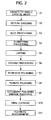
- FIG. 2 is a flow chart showing a manufacturing method for the semiconductor wafer 1 according to the present embodiment. As shown in FIG. 2 , the manufacturing method for the semiconductor wafer 1 according to the present embodiment includes the following steps S1 to S11.
- a single crystal semiconductor ingot is grown by Czochralski method (CZ method), floating zone melting method (FZ method), or the like.
- the semiconductor ingot grown through the single crystal ingot growth step S1 has a front end portion and a rear end portion thereof cut off. Since the semiconductor ingot after being cut has a distorted outline shape, in the outline grinding step, outline of the semiconductor ingot is ground by a cylindrical grinder or the like to trim the outline shape and give a block body having a uniform diameter.
- An orientation flat or orientation notch is formed on the block body after the outline grinding step S2, to indicate a particular crystal orientation.
- the block body is sliced with a wire saw or the like to give a wafer.
- a wafer obtained as a result of the slice processing step S3 is chamfered on a periphery thereof to prevent cracking and chipping on the periphery thereof.
- the peripheral portion of the wafer is chamfered into a predetermined shape by means of a chamfering grindstone.
- the peripheral portion of the wafer is formed into a shape with a predetermined roundness.
- a rough layer on each surface of the wafer of a thin disk shape, generated by processing such as slicing, is made flat by lapping.
- the wafer is disposed between lapping plates that are parallel to each other, and a lapping liquid, which is a mixture of alumina abrasive grains, a dispersing agent, and water, is poured in between the lapping plates and the wafer.
- a lapping liquid which is a mixture of alumina abrasive grains, a dispersing agent, and water, is poured in between the lapping plates and the wafer.
- the lapping plates and the wafer are rotated and ground together under pressure, thereby lapping both surfaces of the wafer. This can improve the flatness of each surface and the parallelism of both surfaces of the wafer.
- the wafer is dipped in an etching solution and etched.
- the etching solution is supplied on a surface of the wafer while the wafer is spun by means of an etching device, for example. Then the etching solution being supplied spreads on a whole surface of the wafer by a centrifugal force of spinning, thereby etching the whole surface of the wafer and controlling surface roughness Ra of the surface of the wafer to be a predetermined surface roughness.
- a work-affected layer introduced by the mechanical processes such as the chamfering step S4 and lapping step S5 is completely removed by etching.
- a peripheral portion of the wafer is subjected to periphery polishing.
- the chamfered surface of the wafer is thus mirror-polished.
- the periphery polishing step the chamfered surface of the wafer is pressed against a peripheral surface of a polishing cloth circulating about an axis, while supplying polishing liquid, thereby mirror-polishing the chamfered surface.
- the wafer is subjected to primary polishing as coarse polishing of surfaces thereof, using a simultaneous double side polishing device that polishes both surfaces simultaneously.
- the wafer is subjected to secondary polishing as mirror polishing, using a simultaneous double side polishing device that polishes both surfaces simultaneously. It should be noted that, although both surfaces of the wafer are simultaneously polished by simultaneous double side polishing in the primary polishing step S8 and the secondary polishing step S9, the wafer can also be polished by single side polishing that polishes one surface thereof at a time.
- the wafer is subjected to final cleaning. More specifically, after the secondary polishing step S9, the wafer is cleaned with RCA cleaning solution.
- flatness of the wafer is measured as a finish level of polishing.
- the wafer 1 having the diameter ⁇ of 450 mm and the thickness t of at least 725 ⁇ m and no greater than 900 ⁇ m can be obtained by the manufacturing steps as described in the abovementioned steps S1 to S11.
- the thickness t thereof is at least 725 ⁇ m
- an amount of deflection of the wafer 1 is equivalent to that of conventional semiconductor wafers in designing and manufacturing of a storage container, a processing device and the like. Therefore, a storage container, a processing device and the like can be designed and manufactured more easily. For example, loading and unloading of the wafer 1 in a storage container, and various handlings of the wafer 1 by a processing device and the like are possible.
- wafers can be prevented from contacting each other and a member that is supposed not to be contacted, thereby preventing scratching, breakage, cracking and the like of the wafers.
- the thickness t of the wafer 1 is no greater than 900 ⁇ m, an increase in weight thereof and an increase in amount of wafer material used can be prevented, thereby avoiding an increase in cost of the wafer 1.
- FIG. 3 is a plan view showing a measuring method of an amount of deflection of the wafer 1.
- FIG. 3 four holding members P1 to P4 are disposed at predetermined positions on a horizontal base 2.
- the wafer 1 having a diameter ⁇ of 450 mm is placed such that an edge portion thereof (shown by two-dot chain line in FIG. 3 ) is supported by the four holding members P1 to P4.
- the holding members P1 and P4 are disposed at positions displaced from each other by 180°, across a center C of the wafer 1.
- the holding members P2 and P3 are disposed symmetrically across an edge portion (a), with an interspace of 200 mm.
- the edge portion (a) is an edge portion of the wafer 1.
- the edge portion (a) is at a position displaced by 90° from the holding member P1 and the holding member P4 respectively.
- Such an arrangement of the holding members P1 to P4 is a model arrangement of positions where a reverse side of a wafer is held in a storage container, in a case where the wafer 1 is loaded in a wafer storage container (FOSB).
- FOSB wafer storage container
- five levels of different thicknesses level 1: 0.779 mm, level 2: 0.826 mm, level 3: 0.900 mm, level 4: 1.012 mm, and level 5: 2.338 mm
- the levels 1 to 3 are examples of the present invention.
- the levels 4 and 5 are comparative examples of the present invention.
- a contacting width L 1 is defined at a position where length of the edge portion of the wafer 1 contacting the holding member P1 is the greatest.
- the contacting width L1 is 7.5 mm in length, from the edge portion of the wafer 1 toward the center C of the wafer 1.
- a contacting width L4 is defined at a position where length of the edge portion of the wafer 1 contacting the holding member P4 is the greatest.
- the contacting width L4 is 7.5 mm in length, from the edge portion of the wafer 1 toward the center C of the wafer 1.
- a position 10 mm away from a predetermined edge portion (a) of the wafer 1 toward a center of the wafer is taken as a position A.
- a position 10 mm away from a predetermined edge portion (b) of the wafer 1 toward a center of the wafer is taken as a position B.
- the edge portion (b) is a position displaced by 180° from the edge portion (a), across a center C of the wafer 1.
- a midpoint between the center C of the wafer 1 and the edge portion (a) (a position ⁇ /4 away from the center C of the wafer) is taken as a position D.
- a midpoint between the center C of the wafer 1 and the edge portion (b) (a position ⁇ /4 away from the center C of the wafer) is taken as a position E.
- an amount of deflection of the wafer was measured optically, from the position A to the position B, at the position A, the position D, the center C of the wafer, the position E, and the position B.
- an amount of deflection of the edge portion of the wafer on the holding members P1 to P4 was used (amount of deflection: 0).
- FIG. 4 is a diagram showing a relationship between thickness of the wafer and the amount of deflection at a position B, measured by the measuring method shown in FIG. 3 .
- the amount of vertically downward deflection of the wafer 1 is hereinafter referred to as amount of negative (-) deflection.
- amount of vertically upward deflection of the wafer 1 is hereinafter referred to as amount of positive (+) deflection.
- the amount of deflection did not simply become greater as thickness of the wafer became smaller, and a peak value of the amount of deflection was obtained with the level 3 (0.900 mm in thickness).
- FIG. 5 is a chart showing a relationship between each measured position on the wafer and the amount of deflection, measured by the measuring method shown in FIG 3 .
- the amount of deflection of the wafer tends to become greater approaching the position B, which is away from the holding members P2 and P3, and moving away from the position A that is close to the positions supported by the holding members P2 and P3. This tendency is particularly significant with the level 1 to the level 4.
- FIG. 6 is a plan view showing another measuring method of the amount of deflection of the wafer 1.
- two holding members P5 and P6 are disposed at predetermined positions on a horizontal base 3.
- the wafer 1 having a diameter ⁇ of 450 mm is placed such that an edge portion thereof (shown by two-dot chain line in FIG. 6 ) is supported by the two holding member P5 and P6.
- the holding members P5 and P6 are disposed at positions displaced from each other by 180°, across a center C of the wafer 1.
- Such an arrangement of the holding members P5 and P6 is a model arrangement of positions where a reverse side of a wafer is held in a processing device or the like, in a case where the wafer 1 is supported by a processing device and the like.
- the edge portion (g) is an edge of the wafer 1.
- the edge portion (g) is at a position displaced by 90° from the holding member P5 and the holding member P6 respectively.
- the edge portion (h) is a position displaced by 90° from the edge portion (g).
- the edge portion (h) overlaps the holding member P6.
- five levels with different thicknesses level 1: 0.779 mm, level 2: 0.826 mm, level 3: 0.900 mm, level 4: 1.012 mm, and level 5: 2.338 mm
- the levels 1 to 3 are examples of the present invention.
- the levels 4 and 5 are comparative examples of the present invention.
- a contacting width L5 is defined at a position where length of the edge portion of the wafer 1 contacting the holding member P5 is the greatest.
- the contacting width L5 is 25 mm in length, from the edge portion of the wafer 1 toward the center F of the wafer 1.
- the contacting width L6 is defined at a position where length of the edge portion of the wafer 1 contacting the holding member P6 is the greatest.
- the contacting width L6 is 25 mm in length, from the edge portion of the wafer 1 toward the center F of the wafer 1.
- a position 10 mm away from a predetermined edge portion (g) of the wafer 1 toward a center of the wafer is taken as a position G.
- a position 10 mm away from a predetermined edge portion (h) of the wafer 1 toward a center of the wafer is taken as a position H.
- Positions 50 mm, 100 mm, 150 mm, and 200 mm away from the center F toward the position G are taken as positions I, J, K and L, respectively.
- Positions 50 mm, 100 mm, 150 mm, and 200 mm away from the center F toward the position H are taken as positions M, N, O and Q, respectively.
- amount of deflection of the wafer was measured optically at the center F, the position I, the position J, the position K, and the position L.
- amount of deflection of the wafer was measured optically at the center F, the position M, the position N, the position O, and the position Q.
- amount of deflection of the position Q supported by the holding member P6 was used (amount of deflection: 0).
- FIGS. 7A and 7B are charts showing a relationship between each measured position on the wafer and the amount of deflection, measured by the measuring method shown in FIG. 6 .
- FIG. 7A is a chart showing a relationship between each measured position on the wafer, from the center F to the position G, and the amount of deflection.
- FIG. 7B is a chart showing a relationship between each measured position on the wafer, from the center F to the position H, and the amount of deflection.
- the amount of deflection of the wafer tends to become greater as a measured position approaches the edge portion (g) of the wafer 1 that is not supported by the holding members P5 and P6, away from the center F.
- the amount of deflection of the wafer tends to become greater as a measured position approaches the center F that is not supported by the holding members P5 and P6, away from the position H that is supported by the holding member P6.
- FIGS. 8A and 8B are charts showing a relationship between thickness of each wafer and the amount of deflection, measured by the measuring method shown in FIG. 6 .
- FIG. 8A is a chart showing a relationship between thickness and the amount of deflection at the center F.
- FIG. 8B is a chart showing a relationship between thickness and the amount of deflection at the position G.
- the amount of deflection of the wafer tends to become greater as the thickness of the wafer becomes smaller.
- FIG. 8B a similar tendency is observed at the position G, with a greater amount of deflection than at the center F. The amount of deflection did not simply become greater as thickness of the wafer became smaller, and a peak value of the amount of deflection was obtained with the level 3 (0.900 mm in thickness).
- FIG. 9 is a chart showing a relationship between thickness of a wafer and the amount of deflection, based on the result of FIGS. 3 to 8B .
- a measured result R shows a result of measurement at the center F according to the abovementioned measuring method shown in FIG. 6 .
- a measured result T shows a result of measurement at the position G according to the abovementioned measuring method shown in FIG. 6 .
- a measured result U shows a result of measurement at the center C according to the abovementioned measuring method shown in FIG. 3 .
- a measured result V shows a result of measurement at the position B according to the abovementioned measuring method shown in FIG. 3 .
- a chart X (two-dot chain line) is a chart showing a relationship between the thickness of the wafer and the amount of deflection, which is calculated from the measured result at the position B according to the abovementioned measuring method shown in FIG. 3 .
- a chart W (dashed-dotted line) is a chart showing a relationship between the thickness of the wafer and the amount of deflection, which is calculated from the measured result at the position G according to the abovementioned measuring method shown in FIG. 6 .
- a chart Y is a chart showing a relationship between the thickness of the wafer and an acceptable value of the amount of deflection in a case where a storage container and a processing device and the like, to which an amount of deflection of the conventional wafer is applied, are used, in consideration of a margin required for loading and unloading the wafer from the storage container by the processing device and the like.
- an intersection point of the chart X and the chart Y corresponds to a thickness of the wafer of 725 ⁇ m. Therefore, in a case where the thickness of the wafer is at least 725 ⁇ m, loading and unloading of the wafer by a processing device and the like from a storage container is possible.
- an intersecting point of the measured result V and the chart Y corresponds to a thickness of the wafer of 900 ⁇ m. Therefore, in a case where the thickness of the wafer is no greater than 900 ⁇ m, loading and unloading of the wafer by a processing device and the like from a storage container is possible.
Landscapes
- Chemical & Material Sciences (AREA)
- Engineering & Computer Science (AREA)
- Crystallography & Structural Chemistry (AREA)
- Materials Engineering (AREA)
- Metallurgy (AREA)
- Organic Chemistry (AREA)
- Container, Conveyance, Adherence, Positioning, Of Wafer (AREA)
- Testing Or Measuring Of Semiconductors Or The Like (AREA)
- Crystals, And After-Treatments Of Crystals (AREA)
Abstract
Description
- This application is based on and claims the benefit of priority from Japanese Patent Application No.
2008-139264, filed on 28 May 2008 - The present invention relates to a semiconductor wafer.
- Recently, size of a semiconductor wafer (hereinafter also referred to simply as "wafer") used for manufacturing a semiconductor device is required to be larger, as size of chips increases in accordance with high integration and functionality of semiconductor devices.
- However, a large diameter wafer may cause various problems during manufacture. For example, Japanese Unexamined Patent Application Publication No.
2004-95942 - The disclosure in
Patent Document 1 is regarding a wafer that has become thin after grinding of a reverse side thereof; however, also in a case of a large diameter semiconductor wafer, increased amount of deflection due to the wafer's own weight leads to a problem in loading and unloading of a wafer in a storage container and a problem of transportability of a wafer in a processing device, a manufacturing device, and the like. - Given this, the present invention aims at providing a semiconductor wafer that enables loading and unloading thereof with regard to a storage container, and transportation thereof, in a processing device, a manufacturing device, and the like.
- In a first aspect of the present invention, a semiconductor wafer has a diameter of 450 mm and a thickness of at least 725 µm and no greater than 900 µm.
- According to the present invention, a semiconductor wafer that enables loading and unloading thereof with regard to a storage container, and transportation thereof, in a processing device, a manufacturing device, and the like can be provided.
-
-
FIGS. 1A to 1C are diagrams illustrating an embodiment of asemiconductor wafer 1 according to the present invention; -
FIG. 1A is a perspective view; -
FIG. 1B is a diagram illustrating thesemiconductor wafer 1 seen from a thickness direction; -
FIG. 1C is a diagram illustrating thesemiconductor wafer 1 seen from a diameter direction; -
FIG. 2 is a flow chart showing manufacturing steps of thesemiconductor wafer 1 according to the present embodiment; -
FIG. 3 is a plan view showing a measuring method of an amount of deflection of thewafer 1; -
FIG. 4 is a diagram showing a relationship between thickness of the wafer and the amount of deflection at a position B, measured by the measuring method shown inFIG. 3 ; -
FIG. 5 is a chart showing a relationship between each measured position on the wafer and the amount of deflection, measured by the measuring method shown inFIG. 3 ; -
FIG. 6 is a plan view showing another measuring method of an amount of deflection of thewafer 1; -
FIGS. 7A and 7B are charts showing a relationship between each measured position on the wafer and the amount of deflection, measured by the measuring method shown inFIG. 6 ; -
FIG. 7A is a chart showing a relationship between each measured position on the wafer, from a center F to a position G, and the amount of deflection; -
FIG. 7B is a chart showing a relationship between each measured position on the wafer, from a center F to a position H, and the amount of deflection; -
FIGS. 8A and 8B are charts showing a relationship between thickness of each wafer and the amount of deflection, measured by the measuring method shown inFIG. 6 ; -
FIG. 8A is a chart showing a relationship between thickness and the amount of deflection at the center F; -
FIG. 8B is a chart showing a relationship between thickness and the amount of deflection at the position H; and -
FIG. 9 is a chart showing a relationship between thickness of a wafer and the amount of deflection, based on the result ofFIGS. 3 to 8B . - An embodiment of the semiconductor wafer according to the present invention is hereinafter described with reference to the drawings.
FIGS. 1A to 1C are diagrams illustrating an embodiment of asemiconductor wafer 1 according to the present invention:FIG. 1A is a perspective view,FIG. 1B is a diagram illustrating thesemiconductor wafer 1 seen from a thickness direction, andFIG. 1C is a diagram illustrating thesemiconductor wafer 1 seen from a diameter direction. - A semiconductor wafer 1 (hereinafter also referred to simply as "wafer") according to the present embodiment has a diameter of 450 mm and a thickness of at least 725 µm and no greater than 900 µm.
- In addition, the
wafer 1 according to the present embodiment is, for example, a silicon wafer or a gallium arsenide wafer. - As shown in
FIGS. 1A and 1B , thewafer 1 according to the present embodiment has a diameter ø of 450 mm. Here, the diameter ø of thewafer 1 is a desired value in manufacturing, and includes an allowable margin of error and the like in manufacturing. For example, the diameter ø of thewafer 1 includes an allowable margin of error of ± 0.2 mm. - In the
wafer 1 according to the present embodiment, a thickness t shown inFIG. 1C is at least 725 µm. The significance thereof is that, in a case where thewafer 1 has the diameter ø of 450 mm and the thickness t of at least 725 µm, an amount of deflection of thewafer 1 is equivalent to that of conventional semiconductor wafers and therefore a storage container, a manufacturing device and the like of thewafer 1 can be designed and manufactured by applying the amount of deflection of the conventional semiconductor wafers. The thickness t is preferably at least 800 µm. - An evaluation example showing that the amount of deflection of the
wafer 1 is equivalent to that of the conventional semiconductor wafers is described later in detail in the EXAMPLE section. - In addition, the
wafer 1 according to the present embodiment has the thickness t no greater than 900 µm. The significance thereof is that an increase in cost of thewafer 1 can be avoided. In a case where the thickness t exceeds 900 µm, thewafer 1 increases in weight and a larger amount of material is required, and therefore thewafer 1 increases in cost. The thickness t is preferably no greater than 850 µm. - A manufacturing method for the
wafer 1 according to the present embodiment is hereinafter described.FIG. 2 is a flow chart showing a manufacturing method for thesemiconductor wafer 1 according to the present embodiment. As shown inFIG. 2 , the manufacturing method for thesemiconductor wafer 1 according to the present embodiment includes the following steps S1 to S11. - First, a single crystal semiconductor ingot is grown by Czochralski method (CZ method), floating zone melting method (FZ method), or the like.
- The semiconductor ingot grown through the single crystal ingot growth step S1 has a front end portion and a rear end portion thereof cut off. Since the semiconductor ingot after being cut has a distorted outline shape, in the outline grinding step, outline of the semiconductor ingot is ground by a cylindrical grinder or the like to trim the outline shape and give a block body having a uniform diameter.
- An orientation flat or orientation notch is formed on the block body after the outline grinding step S2, to indicate a particular crystal orientation. After the processing, the block body is sliced with a wire saw or the like to give a wafer.
- A wafer obtained as a result of the slice processing step S3 is chamfered on a periphery thereof to prevent cracking and chipping on the periphery thereof. In other words, the peripheral portion of the wafer is chamfered into a predetermined shape by means of a chamfering grindstone. By the processing, the peripheral portion of the wafer is formed into a shape with a predetermined roundness.
- After the chamfering step S4, a rough layer on each surface of the wafer of a thin disk shape, generated by processing such as slicing, is made flat by lapping. In the lapping step, the wafer is disposed between lapping plates that are parallel to each other, and a lapping liquid, which is a mixture of alumina abrasive grains, a dispersing agent, and water, is poured in between the lapping plates and the wafer. Thereafter, the lapping plates and the wafer are rotated and ground together under pressure, thereby lapping both surfaces of the wafer. This can improve the flatness of each surface and the parallelism of both surfaces of the wafer.
- After the lapping step S5, the wafer is dipped in an etching solution and etched. In the etching step, the etching solution is supplied on a surface of the wafer while the wafer is spun by means of an etching device, for example. Then the etching solution being supplied spreads on a whole surface of the wafer by a centrifugal force of spinning, thereby etching the whole surface of the wafer and controlling surface roughness Ra of the surface of the wafer to be a predetermined surface roughness. In this etching step, a work-affected layer introduced by the mechanical processes such as the chamfering step S4 and lapping step S5 is completely removed by etching.
- After the etching step S6, a peripheral portion of the wafer is subjected to periphery polishing. The chamfered surface of the wafer is thus mirror-polished. In the periphery polishing step, the chamfered surface of the wafer is pressed against a peripheral surface of a polishing cloth circulating about an axis, while supplying polishing liquid, thereby mirror-polishing the chamfered surface.
- After the periphery polishing step S7, the wafer is subjected to primary polishing as coarse polishing of surfaces thereof, using a simultaneous double side polishing device that polishes both surfaces simultaneously.
- After the primary polishing step S8, the wafer is subjected to secondary polishing as mirror polishing, using a simultaneous double side polishing device that polishes both surfaces simultaneously. It should be noted that, although both surfaces of the wafer are simultaneously polished by simultaneous double side polishing in the primary polishing step S8 and the secondary polishing step S9, the wafer can also be polished by single side polishing that polishes one surface thereof at a time.
- After the secondary polishing (mirror polishing) step S9, the wafer is subjected to final cleaning. More specifically, after the secondary polishing step S9, the wafer is cleaned with RCA cleaning solution.
- After the final cleaning step S10, flatness of the wafer is measured as a finish level of polishing.
- The
wafer 1 having the diameter ø of 450 mm and the thickness t of at least 725 µm and no greater than 900 µm can be obtained by the manufacturing steps as described in the abovementioned steps S1 to S11. - In the
wafer 1 according to the present embodiment, since the thickness t thereof is at least 725 µm, an amount of deflection of thewafer 1 is equivalent to that of conventional semiconductor wafers in designing and manufacturing of a storage container, a processing device and the like. Therefore, a storage container, a processing device and the like can be designed and manufactured more easily. For example, loading and unloading of thewafer 1 in a storage container, and various handlings of thewafer 1 by a processing device and the like are possible. In addition, in the storage container, the processing device and the like, wafers can be prevented from contacting each other and a member that is supposed not to be contacted, thereby preventing scratching, breakage, cracking and the like of the wafers. - Furthermore, with the
wafer 1 according to the present embodiment, since the thickness t of thewafer 1 is no greater than 900 µm, an increase in weight thereof and an increase in amount of wafer material used can be prevented, thereby avoiding an increase in cost of thewafer 1. - Next, the present invention is described further in detail using examples. The examples are not intended to limit the scope of the present invention.
- First, Evaluation Example 1 for an amount of deflection of the
wafer 1 is described hereinafter.FIG. 3 is a plan view showing a measuring method of an amount of deflection of thewafer 1. - As shown in
FIG. 3 , four holding members P1 to P4 are disposed at predetermined positions on ahorizontal base 2. Thewafer 1 having a diameter ø of 450 mm is placed such that an edge portion thereof (shown by two-dot chain line inFIG. 3 ) is supported by the four holding members P1 to P4. The holding members P1 and P4 are disposed at positions displaced from each other by 180°, across a center C of thewafer 1. The holding members P2 and P3 are disposed symmetrically across an edge portion (a), with an interspace of 200 mm. The edge portion (a) is an edge portion of thewafer 1. The edge portion (a) is at a position displaced by 90° from the holding member P1 and the holding member P4 respectively. - Such an arrangement of the holding members P1 to P4 is a model arrangement of positions where a reverse side of a wafer is held in a storage container, in a case where the
wafer 1 is loaded in a wafer storage container (FOSB). As thewafer 1, five levels of different thicknesses (level 1: 0.779 mm, level 2: 0.826 mm, level 3: 0.900 mm, level 4: 1.012 mm, and level 5: 2.338 mm) were provided. Thelevels 1 to 3 are examples of the present invention. And thelevels 4 and 5 are comparative examples of the present invention. - The
wafer 1 of each of thelevels 1 to 5 is placed on the holding members P1 to P4. Here, a contactingwidth L 1 is defined at a position where length of the edge portion of thewafer 1 contacting the holding member P1 is the greatest. The contacting width L1 is 7.5 mm in length, from the edge portion of thewafer 1 toward the center C of thewafer 1. Similarly, a contacting width L4 is defined at a position where length of the edge portion of thewafer 1 contacting the holding member P4 is the greatest. The contacting width L4 is 7.5 mm in length, from the edge portion of thewafer 1 toward the center C of thewafer 1. - Here, a position 10 mm away from a predetermined edge portion (a) of the
wafer 1 toward a center of the wafer is taken as a position A. In addition, a position 10 mm away from a predetermined edge portion (b) of thewafer 1 toward a center of the wafer is taken as a position B. The edge portion (b) is a position displaced by 180° from the edge portion (a), across a center C of thewafer 1. A midpoint between the center C of thewafer 1 and the edge portion (a) (a position ø/4 away from the center C of the wafer) is taken as a position D. In addition, a midpoint between the center C of thewafer 1 and the edge portion (b) (a position ø/4 away from the center C of the wafer) is taken as a position E. - Subsequently, an amount of deflection of the wafer was measured optically, from the position A to the position B, at the position A, the position D, the center C of the wafer, the position E, and the position B. As a reference value of the amount of deflection, an amount of deflection of the edge portion of the wafer on the holding members P1 to P4 was used (amount of deflection: 0).
-
FIG. 4 is a diagram showing a relationship between thickness of the wafer and the amount of deflection at a position B, measured by the measuring method shown inFIG. 3 . The amount of vertically downward deflection of thewafer 1 is hereinafter referred to as amount of negative (-) deflection. On the other hand, the amount of vertically upward deflection of thewafer 1 is hereinafter referred to as amount of positive (+) deflection. - As shown in
FIG. 4 , the amount of deflection did not simply become greater as thickness of the wafer became smaller, and a peak value of the amount of deflection was obtained with the level 3 (0.900 mm in thickness). -
FIG. 5 is a chart showing a relationship between each measured position on the wafer and the amount of deflection, measured by the measuring method shown inFIG 3 . - As shown in
FIG. 5 , the amount of deflection of the wafer tends to become greater approaching the position B, which is away from the holding members P2 and P3, and moving away from the position A that is close to the positions supported by the holding members P2 and P3. This tendency is particularly significant with thelevel 1 to the level 4. - Next, Evaluation Example 2 for amount of deflection of the
wafer 1 is described hereinafter.FIG. 6 is a plan view showing another measuring method of the amount of deflection of thewafer 1. - As shown in
FIG. 6 , two holding members P5 and P6 are disposed at predetermined positions on ahorizontal base 3. Thewafer 1 having a diameter ø of 450 mm is placed such that an edge portion thereof (shown by two-dot chain line inFIG. 6 ) is supported by the two holding member P5 and P6. The holding members P5 and P6 are disposed at positions displaced from each other by 180°, across a center C of thewafer 1. Such an arrangement of the holding members P5 and P6 is a model arrangement of positions where a reverse side of a wafer is held in a processing device or the like, in a case where thewafer 1 is supported by a processing device and the like. - Here, length in the longitudinal direction of the holding members P5 and P6 is 550 mm. A distance between the holding member P5 and the holding member P6 is 400 mm. The edge portion (g) is an edge of the
wafer 1. The edge portion (g) is at a position displaced by 90° from the holding member P5 and the holding member P6 respectively. The edge portion (h) is a position displaced by 90° from the edge portion (g). The edge portion (h) overlaps the holding member P6. As thewafer 1, five levels with different thicknesses (level 1: 0.779 mm, level 2: 0.826 mm, level 3: 0.900 mm, level 4: 1.012 mm, and level 5: 2.338 mm) were provided as in Evaluation Example 1. Thelevels 1 to 3 are examples of the present invention. Thelevels 4 and 5 are comparative examples of the present invention. - The
wafer 1 of each of thelevels 1 to 5 is placed on the holding members P5 and P6. Here, a contacting width L5 is defined at a position where length of the edge portion of thewafer 1 contacting the holding member P5 is the greatest. The contacting width L5 is 25 mm in length, from the edge portion of thewafer 1 toward the center F of thewafer 1. Similarly, the contacting width L6 is defined at a position where length of the edge portion of thewafer 1 contacting the holding member P6 is the greatest. The contacting width L6 is 25 mm in length, from the edge portion of thewafer 1 toward the center F of thewafer 1. - Here, a position 10 mm away from a predetermined edge portion (g) of the
wafer 1 toward a center of the wafer is taken as a position G. Here, a position 10 mm away from a predetermined edge portion (h) of thewafer 1 toward a center of the wafer is taken as a position H. Positions 50 mm, 100 mm, 150 mm, and 200 mm away from the center F toward the position G are taken as positions I, J, K and L, respectively.Positions 50 mm, 100 mm, 150 mm, and 200 mm away from the center F toward the position H are taken as positions M, N, O and Q, respectively. - Subsequently, amount of deflection of the wafer was measured optically at the center F, the position I, the position J, the position K, and the position L. In addition, amount of deflection of the wafer was measured optically at the center F, the position M, the position N, the position O, and the position Q. As a reference value of the amount of deflection, amount of deflection of the position Q supported by the holding member P6 was used (amount of deflection: 0).
-
FIGS. 7A and 7B are charts showing a relationship between each measured position on the wafer and the amount of deflection, measured by the measuring method shown inFIG. 6 .FIG. 7A is a chart showing a relationship between each measured position on the wafer, from the center F to the position G, and the amount of deflection.FIG. 7B is a chart showing a relationship between each measured position on the wafer, from the center F to the position H, and the amount of deflection. - As shown in
FIG. 7A , the amount of deflection of the wafer tends to become greater as a measured position approaches the edge portion (g) of thewafer 1 that is not supported by the holding members P5 and P6, away from the center F. - In addition, as shown in
FIG. 7B , the amount of deflection of the wafer tends to become greater as a measured position approaches the center F that is not supported by the holding members P5 and P6, away from the position H that is supported by the holding member P6. -
FIGS. 8A and 8B are charts showing a relationship between thickness of each wafer and the amount of deflection, measured by the measuring method shown inFIG. 6 .FIG. 8A is a chart showing a relationship between thickness and the amount of deflection at the center F.FIG. 8B is a chart showing a relationship between thickness and the amount of deflection at the position G. - As shown in
FIG. 8A , at the center F, the amount of deflection of the wafer tends to become greater as the thickness of the wafer becomes smaller. In addition, as shown inFIG. 8B , a similar tendency is observed at the position G, with a greater amount of deflection than at the center F. The amount of deflection did not simply become greater as thickness of the wafer became smaller, and a peak value of the amount of deflection was obtained with the level 3 (0.900 mm in thickness). -
FIG. 9 is a chart showing a relationship between thickness of a wafer and the amount of deflection, based on the result ofFIGS. 3 to 8B . - As shown in
FIG. 9 , a measured result R (triangle) shows a result of measurement at the center F according to the abovementioned measuring method shown inFIG. 6 . A measured result T (circle) shows a result of measurement at the position G according to the abovementioned measuring method shown inFIG. 6 . A measured result U (square) shows a result of measurement at the center C according to the abovementioned measuring method shown inFIG. 3 . A measured result V (diamond) shows a result of measurement at the position B according to the abovementioned measuring method shown inFIG. 3 . - In addition, a chart X (two-dot chain line) is a chart showing a relationship between the thickness of the wafer and the amount of deflection, which is calculated from the measured result at the position B according to the abovementioned measuring method shown in
FIG. 3 . A chart W (dashed-dotted line) is a chart showing a relationship between the thickness of the wafer and the amount of deflection, which is calculated from the measured result at the position G according to the abovementioned measuring method shown inFIG. 6 . Furthermore, a chart Y (full line) is a chart showing a relationship between the thickness of the wafer and an acceptable value of the amount of deflection in a case where a storage container and a processing device and the like, to which an amount of deflection of the conventional wafer is applied, are used, in consideration of a margin required for loading and unloading the wafer from the storage container by the processing device and the like. - As shown in
FIG. 9 , an intersection point of the chart X and the chart Y corresponds to a thickness of the wafer of 725 µm. Therefore, in a case where the thickness of the wafer is at least 725 µm, loading and unloading of the wafer by a processing device and the like from a storage container is possible. In addition, an intersecting point of the measured result V and the chart Y corresponds to a thickness of the wafer of 900 µm. Therefore, in a case where the thickness of the wafer is no greater than 900 µm, loading and unloading of the wafer by a processing device and the like from a storage container is possible.
Claims (1)
- A semiconductor wafer having a diameter of 450 mm and a thickness of at least 725 µm and no greater than 900 µm.
Applications Claiming Priority (1)
| Application Number | Priority Date | Filing Date | Title |
|---|---|---|---|
| JP2008139264A JP2009289877A (en) | 2008-05-28 | 2008-05-28 | Semiconductor wafer |
Publications (2)
| Publication Number | Publication Date |
|---|---|
| EP2128895A2 true EP2128895A2 (en) | 2009-12-02 |
| EP2128895A3 EP2128895A3 (en) | 2010-01-27 |
Family
ID=40909997
Family Applications (1)
| Application Number | Title | Priority Date | Filing Date |
|---|---|---|---|
| EP09161252A Withdrawn EP2128895A3 (en) | 2008-05-28 | 2009-05-27 | Semiconductor wafer |
Country Status (3)
| Country | Link |
|---|---|
| US (1) | US20090297755A1 (en) |
| EP (1) | EP2128895A3 (en) |
| JP (1) | JP2009289877A (en) |
Families Citing this family (1)
| Publication number | Priority date | Publication date | Assignee | Title |
|---|---|---|---|---|
| JP6244962B2 (en) * | 2014-02-17 | 2017-12-13 | 株式会社Sumco | Manufacturing method of semiconductor wafer |
Citations (1)
| Publication number | Priority date | Publication date | Assignee | Title |
|---|---|---|---|---|
| JP2004095942A (en) | 2002-09-02 | 2004-03-25 | Kokusai Electric Semiconductor Service Inc | Wafer cassette |
Family Cites Families (3)
| Publication number | Priority date | Publication date | Assignee | Title |
|---|---|---|---|---|
| JP4424039B2 (en) * | 2004-04-02 | 2010-03-03 | 株式会社Sumco | Manufacturing method of semiconductor wafer |
| JP5087855B2 (en) * | 2006-04-05 | 2012-12-05 | 株式会社Sumco | Heat treatment evaluation wafer, heat treatment evaluation method, and semiconductor wafer manufacturing method |
| JP2009141081A (en) * | 2007-12-05 | 2009-06-25 | Sumco Corp | Semiconductor wafer surface inspection equipment |
-
2008
- 2008-05-28 JP JP2008139264A patent/JP2009289877A/en active Pending
-
2009
- 2009-05-26 US US12/471,855 patent/US20090297755A1/en not_active Abandoned
- 2009-05-27 EP EP09161252A patent/EP2128895A3/en not_active Withdrawn
Patent Citations (1)
| Publication number | Priority date | Publication date | Assignee | Title |
|---|---|---|---|---|
| JP2004095942A (en) | 2002-09-02 | 2004-03-25 | Kokusai Electric Semiconductor Service Inc | Wafer cassette |
Also Published As
| Publication number | Publication date |
|---|---|
| JP2009289877A (en) | 2009-12-10 |
| EP2128895A3 (en) | 2010-01-27 |
| US20090297755A1 (en) | 2009-12-03 |
Similar Documents
| Publication | Publication Date | Title |
|---|---|---|
| US7077726B2 (en) | Semiconductor wafer with improved local flatness, and method for its production | |
| EP1501119A1 (en) | Semiconductor wafer manufacturing method and wafer | |
| US6050880A (en) | Surface grinding device and method of surface grinding a thin-plate workpiece | |
| EP2428318A2 (en) | Method of polishing an object to form a convex or concave surface on said object and polishing pad | |
| US6284658B1 (en) | Manufacturing process for semiconductor wafer | |
| JP2003229392A (en) | Method for manufacturing silicon wafer, silicon wafer, and SOI wafer | |
| US6599760B2 (en) | Epitaxial semiconductor wafer manufacturing method | |
| JP2010040549A (en) | Semiconductor wafer and manufacturing method thereof | |
| EP3888846B1 (en) | Semiconductor substrate and method for manufacturing the same | |
| US20090297755A1 (en) | Semiconductor wafer | |
| WO2010016510A1 (en) | Method for manufacturing a semiconductor wafer | |
| US20090311460A1 (en) | Semiconductor wafer | |
| JP5515253B2 (en) | Manufacturing method of semiconductor wafer | |
| JP3516203B2 (en) | Compound semiconductor wafer | |
| JP5343400B2 (en) | Manufacturing method of semiconductor wafer | |
| TWI905030B (en) | Method for manufacturing semiconductor crystal wafer | |
| JP2000091282A (en) | Manufacture of high flatness wafer | |
| JP2001071244A (en) | Precise chamfering method for semiconductor wafer | |
| JPH1131670A (en) | Semiconductor substrate manufacturing method | |
| JP3514108B2 (en) | Wrapping device and method | |
| JPS6381934A (en) | Wafer and manufacture thereof | |
| JP4681970B2 (en) | Polishing pad and polishing machine | |
| JP2009289875A (en) | Semiconductor wafer | |
| TW202505702A (en) | Square silicon substrate and manufacturing method thereof | |
| JP2009283720A (en) | Semiconductor wafer |
Legal Events
| Date | Code | Title | Description |
|---|---|---|---|
| PUAI | Public reference made under article 153(3) epc to a published international application that has entered the european phase |
Free format text: ORIGINAL CODE: 0009012 |
|
| 17P | Request for examination filed |
Effective date: 20090527 |
|
| AK | Designated contracting states |
Kind code of ref document: A2 Designated state(s): AT BE BG CH CY CZ DE DK EE ES FI FR GB GR HR HU IE IS IT LI LT LU LV MC MK MT NL NO PL PT RO SE SI SK TR |
|
| PUAL | Search report despatched |
Free format text: ORIGINAL CODE: 0009013 |
|
| AK | Designated contracting states |
Kind code of ref document: A3 Designated state(s): AT BE BG CH CY CZ DE DK EE ES FI FR GB GR HR HU IE IS IT LI LT LU LV MC MK MT NL NO PL PT RO SE SI SK TR |
|
| AX | Request for extension of the european patent |
Extension state: AL BA RS |
|
| STAA | Information on the status of an ep patent application or granted ep patent |
Free format text: STATUS: THE APPLICATION HAS BEEN WITHDRAWN |
|
| 18W | Application withdrawn |
Effective date: 20100305 |