EP2124124A1 - Controlled current source and method for sourcing a current - Google Patents
Controlled current source and method for sourcing a current Download PDFInfo
- Publication number
- EP2124124A1 EP2124124A1 EP08009393A EP08009393A EP2124124A1 EP 2124124 A1 EP2124124 A1 EP 2124124A1 EP 08009393 A EP08009393 A EP 08009393A EP 08009393 A EP08009393 A EP 08009393A EP 2124124 A1 EP2124124 A1 EP 2124124A1
- Authority
- EP
- European Patent Office
- Prior art keywords
- current
- bus signal
- output
- potential
- signal
- Prior art date
- Legal status (The legal status is an assumption and is not a legal conclusion. Google has not performed a legal analysis and makes no representation as to the accuracy of the status listed.)
- Granted
Links
- 238000012358 sourcing Methods 0.000 title claims abstract description 23
- 238000000034 method Methods 0.000 title claims abstract description 9
- 238000013507 mapping Methods 0.000 claims abstract description 29
- 230000008878 coupling Effects 0.000 claims description 16
- 238000010168 coupling process Methods 0.000 claims description 16
- 238000005859 coupling reaction Methods 0.000 claims description 16
- 230000001105 regulatory effect Effects 0.000 description 3
- 238000005513 bias potential Methods 0.000 description 2
- 238000010586 diagram Methods 0.000 description 2
- 230000001364 causal effect Effects 0.000 description 1
- 238000011217 control strategy Methods 0.000 description 1
- 230000001419 dependent effect Effects 0.000 description 1
- 238000011161 development Methods 0.000 description 1
- 230000018109 developmental process Effects 0.000 description 1
- 229910044991 metal oxide Inorganic materials 0.000 description 1
- 150000004706 metal oxides Chemical class 0.000 description 1
- 239000004065 semiconductor Substances 0.000 description 1
- 230000007704 transition Effects 0.000 description 1
Images




Classifications
-
- G—PHYSICS
- G05—CONTROLLING; REGULATING
- G05F—SYSTEMS FOR REGULATING ELECTRIC OR MAGNETIC VARIABLES
- G05F1/00—Automatic systems in which deviations of an electric quantity from one or more predetermined values are detected at the output of the system and fed back to a device within the system to restore the detected quantity to its predetermined value or values, i.e. retroactive systems
- G05F1/10—Regulating voltage or current
- G05F1/46—Regulating voltage or current wherein the variable actually regulated by the final control device is DC
- G05F1/56—Regulating voltage or current wherein the variable actually regulated by the final control device is DC using semiconductor devices in series with the load as final control devices
Definitions
- the invention relates to a controlled source and to a method for sourcing a current.
- an output current can be generated which is controllable by a certain number of bits to tune the exact value of the output current.
- One existing implementation of such a digitally controlled current source comprises a transistor arrangement for sourcing the output current and a regulation circuit.
- the transistor arrangement and the regulation circuit are coupled to each other via a set of switches which are directed by a control signal comprising a number of bits.
- the number of bits determines the number of levels of the digitally controlled source.
- the number of transistors of the transistor arrangement corresponds to the number of bits.
- the sizes of the transistors are selected in a way that they increase with 2 n , with n ranging from zero to the total number of bits.
- the regulation circuit generates a constant reference current which is used by the transistor arrangement to source the output current depending on the control signal.
- a controlled current source with less power consumption can be necessary.
- a controlled current source comprises a signal input to receive a control input bus signal, a mapping unit, a reference generator and a current generating unit.
- the mapping unit has an input coupled to the signal input and an output to provide an internal control bus signal.
- the reference generator has an input coupled to the output of the mapping unit, a low reference output to provide a low reference potential and a high reference output to provide a high reference potential.
- the current generating unit has a first input coupled to the output of the mapping unit, a second input coupled to the output of the reference generator and an output to provide an output current. The output current is controlled by the control input bus signal and the low and high reference potentials.
- the control input bus signal is applied to the mapping unit.
- the mapping unit provides the internal control bus signal as a function of the control input bus signal.
- the reference generator generates the low and the high reference potentials.
- the current generating unit provides the output current as a function of the control input bus signal using the high and low reference potentials.
- the provisioning of the internal control bus signal is achieved by coding or decoding the control input bus signal.
- the structure of the reference generator acting as a regulation circuit results in two reference potentials: The low reference potential which is used for a first subset of current levels provided by the controlled current source and the high reference potential which is used in addition to the low reference potential for a second subset of current levels provided by the controlled current source. This leads to an improved control strategy with a reduced current consumption and reduced size.
- control input bus signal comprises a binary coded digital signal with n bits.
- the internal control bus signal comprises a binary coded digital signal with (n+1) bits.
- the 2 n step or level linear controlled current source can be designed. For the first subset of current levels ranging from zero to 2 n-1 -1, only the low reference potential is needed. For the second subset of current levels ranging from 2 n-1 to 2 n , the low and the high reference potentials are required to provide the output current.
- the reference generator comprises a second input to receive a first reference current, a second reference current and a defining potential.
- the reference generator By use of the first and second reference currents and the defining potential, the reference generator provides the high and the low reference potentials.
- the current generating unit comprises a coupling unit and a current sourcing array.
- the coupling unit comprises the first input of the current generating unit to receive the internal control bus signal, the second input of the current generating unit to receive the low and the high reference potentials and it comprises an output to provide a gate signal bus.
- the current sourcing array comprises an input coupled to the output of the coupling unit and the output which provides the output current.
- the gate signal bus is generated as a function of the internal control bus signal using the low and/or high reference potentials. Applied to the current sourcing array the gate signal bus drives the level of the output current.
- the current sourcing array comprises an array of transistors coupled in parallel, with their gate terminals coupled to the output of the coupling unit.
- sizes s of the transistors of the array of transistors defined as a quotient of channel width and length are selected as a product of 0.5 and 2 x , with x ranging from 0 to n-1, and a size of the last transistor matching the respective size of the second-last transistor.
- the transistors can be implemented as metal oxide semiconductor, MOS, transistors.
- the transistors of the current sourcing array are operated as current sources with the ability to provide a current with a value depending on the size s of the respective transistor.
- the gate signal bus controls the respective transistor or transistors.
- the reference generator comprises a first and a second equalizer, as well as a first and a second differential amplifier.
- the first equalizer provides a first threshold potential corresponding to the defining potential.
- the second equalizer provides a second threshold potential corresponding to the defining potential.
- the first amplifier provides the low reference potential using the first reference current and a first feedback current at the first threshold potential.
- the second amplifier provides the high reference potential using the second reference current and a second feedback current at the second threshold potential.
- the reference generator maintains the low and the high reference potentials at a constant value respectively.
- control input bus signal comprises an additional control component and the internal control bus signal comprises an additional internal component.
- the additional control component and the additional internal component enable the controlled current source to provide a higher range of current levels using the same number of transistors in the current sourcing array.
- the range of the current source is extended to 2 n + 2 n-1 -1 current levels.
- the internal control bus signal comprises a second additional internal component.
- the resolution of the controlled current source is enhanced.
- a control input bus signal is supplied. Furthermore, a first and a second reference current as well as a defining potential are supplied. An internal control bus signal is provided as a function of the control input bus signal. The internal control bus signal is forwarded to a current generating unit. An output current is generated for a first subset of current levels as a function of the control input bus signal, and a low reference potential, and for a second subset of current levels as a function of the control input bus signal, the low and a high reference potential.
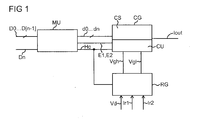
- FIG. 1 shows a first exemplary embodiment of a controlled current source.
- the controlled current source comprises a mapping unit MU, a current generating unit CG and a reference generator RG.
- the mapping MU comprises a signal input to receive a control input bus signal D0 to D(n-1) and a signal output to provide an internal control bus signal d0 to dn and a high control signal Hc.
- the control input bus signal D0 to D(n-1) comprises a binary coded digital signal with n bits.
- the internal control bus signal d0 to dn comprises a binary coded digital signal with (n+1) bits.
- the reference generator RG comprises a first input which is coupled to the output of the mapping unit, and a second input to receive a defining potential Vd, a first reference current Ir1 and a second reference current Ir2.
- the reference generator RG further comprises a reference output to provide a low reference potential Vgl and a high reference output to provide a high reference potential Vgh.
- the current generating unit CG comprises a coupling unit CU and a current sourcing array CS.
- the current generating unit comprises a first input coupled to the output of a mapping unit MU, and a second input to receive the low and the high reference potential.
- the current generating unit CG further comprises an output to provide an output current Iout.
- the n bits of the control input bus signal D0 to D(n-1) are coded into n+1 bits of the internal control bus signal d0 to dn and the high control signal Hc.
- the internal control bus signal d0 to dn and the high control signal Hc are forwarded to the current generating unit CG.
- the high control signal Hc is forwarded to the reference generator RG, as well.
- the reference generator RG generates the low and the high reference potentials Vgl and Vgh using the defining potential Vd, the first and the second reference currents Ir1 and Ir2.
- the output current Iout is generated as a function of the control input bus signal D0 to D(n-1) and the low and the high reference potentials Vgl and Vgh.
- the output current Iout is provided as a multiple of a step current.
- mapping or the coding of the control input bus signal D0 to D(n-1) to the internal control bus signal d0 to dn can be realized as follows:
- the current source is extended to provide 2 n +2 n-1 steps or current levels.
- a respective additional component Dn of the control input bus signal D0 to D(n-1) is supplied to the mapping unit MU.
- a first additional internal component E1 is generated by the mapping unit MU.
- the coding can be realised as follows: The first internal component E1 equals the respective additional component Dn.
- the high control signal Hc, and internal control bus signal bits dn and d(n-1) equal 1 respectively.
- Internal control bus signal bit d(n-2) equals control input bus signal bit D(n-2)
- internal control bus signal bit d(n-3) equals control input bus signal bit D(n-3)
- internal control bus signal bit d(n-4) equals control input bus signal bit D(n-4) and so forth until internal control bus signal bit d0 equals control input bus signal bit D0
- the second additional internal component E2 equals 1, the first additional internal component E1 equals 0, the high control signal Hc equals 0, internal control bus signal bit dn equals 0, internal control bus signal bits dn and d(n-1) equal control input bus signal bit D(n-1), internal control bus signal bit d(n-2) equals control input bus signal bit D(n-2), internal control bus signal bit d(n-3) equals control input bus signal bit D(n-3), and so forth until internal control bus signal bit d0 equals control input bus signal bit D0.
- FIG. 2A shows an exemplary embodiment of a mapping unit of a second exemplary embodiment of a controlled current source.
- the mapping unit MU comprises nine 2:1 multiplexers MX0, MX1, MX2, MX3, MX4, MX5, MX6, MX7, and MX8.
- Each of the multiplexers MX0 to MX8 comprises two data inputs, one data output and one control input.
- Bit D7 of the control input bus signal D0 to D7 is applied to every control input of the multiplexers MX0 to MX8.
- For the multiplexers MX1 to MX7 two consecutive bits of the control input bus signal D0 to D7 are supplied to the respective data inputs, and one bit of the internal control bus signal d0 to d8 is provided at the respective data output.
- the higher bit of the control input bus signal Do to D7 is supplied to the lower data input and the lower bit of the control input bus signal D0 to D7 is supplied to.the upper data input of each multiplexer.
- bit D0 of the control input bus signal D0 to D7 is supplied to the upper data input and the bit D1 of the control input bus signal D0 to D7 is supplied to the lower data input of the multiplexer MX1.
- Bit d1 of the internal control bus signal d0 to d8 is provided at the data output of the multiplexer MX1.
- the upper data input of each multiplexer MX0 to MX8 is forwarded to the respective data output.
- bit D7 of the control input bus signal being at logic 1
- the lower data input of each multiplexer MX0 to MX1 is forwarded to its respective data output.
- bit D0 of the control input bus signal D0 to D7 is multiplexed with logic 0.
- bit D7 of the control input bus signal D0 to D7 is multiplexed with logic 0.
- mapping unit MU depicted in Figure 2A a mapping of codes is realized as demonstrated in Table 1.
- Table 1 shows on the left side all possible codes of the control input bus signal D0 to D7.
- the second half of Table 1 shows the corresponding codes of the internal control bus signal d0 to d8.
- the coding of the high control signal Hc is shown.
- the corresponding values of the output current Iout are depicted in units of the step current Ilsb.
- the value of the high control signal Hc corresponds to the value of bit D7 of the control input bus signal D0 to D7.
- Figure 2B shows an exemplary embodiment of a current generation unit of the second exemplary embodiment of a controlled current source.
- the current generation unit CG can be coupled to the mapping unit MU of Figure 2A .
- Said current generation unit CG comprises a coupling unit CU and a current sourcing array CS.
- the current sourcing array CS comprises an array of nine transistors MP0, MP1, MP2, MP3, MP4, MP5, MP6, MP7, and MP8.
- the transistors MP0 to MP8 are coupled in parallel with their respective source terminals coupled to a source potential Vs and their respective drain terminals coupled to a defining potential Vd.
- Gate terminals of the transistors of the array of transistors MP0 to MP8 are coupled to a gate signal bus g0, g1, g2, g3, g4, g5, g6, g7, and g8.
- gate signal bus component g0 is coupled to the gate of transistor MP0
- gate signal bus component g1 is coupled to the gate of transistor MP1
- gate signal bus component g2 is coupled to transistor MP2's gate
- gate signal bus component g3 is coupled to the gate terminal of transistor MP3
- gate signal bus component g4 is coupled to the gate terminal of transistor MP4
- gate signal bus component g5 is coupled to the gate terminal of transistor MP5
- gate signal bus component g6 is coupled to the gate terminal of transistor MP6
- gate signal bus component g7 is coupled to the gate terminal of transistor MP7
- gate signal bus component g8 is coupled to the gate terminal of transistor MP8.
- the sizes of the transistors MP0 to MP8 are dimensioned such that the respective channel length is always the same, and the channel width increases with a factor of 2 x of a reference width w, starting at half of the reference width w, with x ranging from 0 to 7. It follows that the width of transistor MP0 equals 0.5 w, the width of transistor MP1 equals w, the width of transistor MP2 equals 2w, the width of transistor MP3 equals 4w, the width of transistor MP4 equals 8w, the width of transistor MP5 equals 16w, the width of transistor MP6 equals 32w and the widths of transistors MP7 and MP8 equal 64w.
- Transistors MP0 to MP8 are implemented as p-channel MOS transistors, for example. The coupling of the drain terminals of the transistors MP0 to MP8 to the defining potential Vd also forms the output of the controlled current source which provides an output current Iout.
- the coupling unit CU comprises a first input to receive the internal control bus signal d0 to d8, as well as the high control signal Hc, and a second input to receive the low and the high reference potentials Vgl and Vgh.
- the coupling unit CU further comprises an output to provide the gate signal bus g0 to g8.
- the coupling unit CU also comprises a high switch s0, two low switches s7 and s8, six low-high switches s1, s2, s3, s4, s5 and s6, a first switch sa and a second switch sb, one inverted high switch xs0, two inverted low switches xs7 and xsS8 and six inverted low-high switches xs1, xs2, xs3, xs4, xs5, and xs6, and an inverter N1. All the switches mentioned are logic controlled switches which means that a logic high at the control input of the switch turns the switch on.
- Switches s0 to s8 are controlled by the related bit with the same number of the internal control bus signal d0 to d8, respectively.
- Inverted switches sx0 to sx8 are controlled by the inverted related bit with the same number xd0 to xd8 of the internal control bus signal d0 to d8, respectively.
- the gate terminals of transistors MP1 to MP6 are coupled either to the low reference potential Vgl via the low-high switches s1 to s6, respectively, or they are coupled to the source potential Vs via the inverted low-high switches xs1 to xs6 depending on the value of the bits d1 to d6 of the internal control bus signal d0 to d8, respectively.
- the respective transistor is turned on and contributes with its respective multiple of the step current Ilsb to the output current Iout.
- transistor MP3 contributes with 4 times the step current Ilsb to the output current Iout when turned on.
- the bit d0 of the internal control bus signal d0 to d8 always is 0, the high reference potential Vgh is coupled to the source potential Vs via switch xs0. This means that transistor MP0 stays off. Therefore, the regulation of the output current Iout is achieved by regulating only the low reference potential Vgl.
- the high control signal Hc is at logic high or logic 1. It follows that the second switch sb is closed and the first switch sa is opened via the inverter N1. Therefore, the gate terminals of transistors MP0 to MP6 are either coupled to the high reference potential Vgh or they are coupled to the source potential Vs depending on the value of bits d1 to d6 of the internal control bus signal d0 to d8, respectively. For this span of codes, bits d7 and d8 of the internal control bus signal d0 to d8 are at the value 1 according to Table 1. It follows that the gate terminals of transistors MP7 and MP8 are coupled to the low reference potential Vgl.
- the low reference potential Vgl and the high reference potential both are directing the gates of the transistors MP0 to MP8.
- the step current Ilsb is defined as the current which is provided when bits D1 to D7 of the control input bus signal D0 to D7 are at logic low and bit D0 of the control input bus signal D0 to D7 is at logic high resulting in transistor MP1 being switched on.
- transistor MP7 corresponds to the size of transistor MP8 and equals 64 W, a layout reduction is achieved.
- the current generation unit CG described above can be extended to realize a 2 n step controlled current source by adding supplementary transistors MP9 to MPn to the current sourcing array CS and by using bits D8 to D(n-1) of the control input bus signal and bits d9 to dn of the internal control bus signal as described under Figure 1 . Then sizes of the transistors are chosen as described above for transistors MP0 to MP7. Size of transistor MP8 then equals 128w, size of transistor MP9 equals 256w, and size of transistor MP(n-1) corresponds to the size of transistor MPn.
- Gate terminals of transistors MP(n-1) and MPn can be coupled to the low reference potential Vgl depending upon the corresponding bits d(n-1), dn of the internal control bus signal are at logic zero or one.
- a gate terminal of transistor MP0 can be coupled to the high reference potential Vgh depending upon the corresponding bit d0 of the internal control bus signal is 0 or 1.
- Gate terminals of transistors MP1 to MP(n-1) can either be coupled to the low reference potential Vgl or to the high reference potential Vgh depending upon the high control signal Hc being at logic zero or logic 1 and the corresponding bits d1 to d(n-2) are at logic zero or logic 1.
- the gate terminals of transistors MPn and MP(n-1) are coupled to the low reference potential Vgl if the first additional internal component E1 is at logic zero. If the first additional internal component E1 is at logic 1, the gate terminals of transistors MPn and MP(n-1) are coupled to the high reference potential Vgh.
- the coupling of the gate terminal of transistor MP0 is directed by the second additional internal component E2. If the second additional internal component E2 is at logic zero, the gate of transistor MP0 is coupled to the high reference potential Vgh. If the second additional internal component E2 is at logic one, the gate of transistor MP0 is coupled to the low reference potential Vgl.
- the resolution of the controlled current source is half of the step current Ilsb. A range of 0 to (2 n -1) times half of the step current Ilsb is achieved.
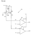
- Figure 2C shows a first exemplary embodiment of a reference generator of the second exemplary embodiment of a controlled current source.
- This embodiment of the reference generator RG comprises a first differential amplifier A0, a second differential amplifier A1, a first equalizer M3, a second equalizer M4 and a control transistor M0.
- the first and the second equalizer M3 and M4 and the control transistor M0 each comprise a p-channel MOS transistor.
- Source terminals of the first and the second equalizer M3 and M4 as well as a source terminal of the control transistor M0 are each coupled to the source potential Vs.
- a drain terminal of the first equalizer M3 is coupled to a first input of the first differential amplifier A0.
- a drain terminal of the second equalizer M4 is coupled to a first input of the second differential amplifier A1.
- a gate terminal of the first equalizer M3 is coupled to the low reference potential Vgl.
- a gate terminal of the control transistor M0 is connected to the high control signal Hc.
- a drain terminal of the control transistor M0 is coupled to a gate terminal of the second equalizer M4 which is coupled to the high reference potential Vgh.
- a first feedback current Is1 is a drain source current of the first equalizer M3.
- a second feedback current Is2 is a drain source current of the second equalizer M4.
- a potential at the drain terminal of the first equalizer M3 is defined as a first threshold potential Vd1.
- a potential at the drain terminal of the second equalizer M4 is defined as a second threshold potential Vd2.
- a first reference current Ir1 is supplied to the second input of the first differential amplifier A0.
- a second reference current Ir2 is supplied to the second input of the second differential amplifier A1.
- the defining potential Vd is supplied to each supply input of the first and the second differential amplifier A0 and A1.
- the first and the second equalizers M3 and M4, as well as the control transistor M0 can be implemented as p-channel MOS transistors, for example.
- the length of the first and the second equalizers M3 and M4 correspond to the lengths of transistors MP0 to MP 8.
- Is1 represents the value of the first feedback current IS1
- Is2 represents the value of the second feedback current IS2
- Ilsb represents the value of the step current Ilsb
- w(M3) represents the value of the with of the first equaliser M3
- w(M4) represents the value of the with of the first equaliser M4
- w represents the value of the reference width w.
- the values for the step current Ilsb, the first and second feedback currents Is1 and Is2 are known from the design respectively.
- the first differential amplifier A0 provides the low reference potential Vgl at its output.
- the low reference potential Vgl is proportional to the difference between the first feedback current Is1 and the first reference current Ir1.
- the first differential amplifier A0 maintains the first threshold potential Vd1 at the defining potential Vd.
- the second differential amplifier A1 provides the high reference potential Vgh at its output.
- the high reference potential Vgh is proportional to the difference between the second feedback current Is2 and the second reference current Ir2.
- the second differential amplifier A1 maintains the second threshold potential Vd2 equal to the defining potential Vd.
- the control transistor M0 ensures that as long as the high control signal Hc is low, the high reference potential Vgh equals the source potential Vs and is not regulated by the second differential amplifier A1. By this, the reduction in power consumption is achieved.
- FIG. 2D shows a second exemplary embodiment of a reference generator of the second exemplary embodiment of a controlled current source.
- This embodiment represents a detailed implementation of the embodiment of the reference generator RG described in Figure 2C .
- This embodiment of the reference generator RG is operated in the same way as described in Figure 2C .
- This embodiment comprises a low regulation loop, a high regulation loop, a generation circuit for the defining potential Vd and the control transistor M0.
- the low regulation loop comprises transistors M2, M6, M11, M12, M15, and the first equalizer M3.
- the high regulation loop comprises transistors M1, M7, M10, M13, M16, and the second equalizer M4.
- the generation circuit for the defining potential Vd comprises transistors M5, M8, M9, M14, M17, and M18.
- Transistor M15 is configured to operate as a current source for the first reference current Ir1.
- Transistor M16 is configured to operate as a current source for the second reference current Ir2.
- Transistors M1, M2, M5, M6, M7, M8, M9, M12, M13, and M14 are implemented as p-channel MOS transistors, for example.
- Transistors M10, M11, M15, M16, M17, and M18 are implemented as n-channel MOS transistors, for example.
- the first feedback current Is1 flowing through the first equalizer M3 as its steady state current is equal to the difference between the first reference current Ir1 and a second bias current Ib2 flowing through transistor M2.
- the second feedback current Is2 which is the steady state current of the second equalizer M4 is equal to the difference between the second reference current Ir2 and a first bias current Ib1 flowing through transistor M1.
- the high control signal Hc is low. Therefore, a gate terminal of the second equalizer M4 is coupled to the source potential Vs. It follows that the second equalizer M4 and the transistors M7, M13, and M10 are turned off.
- w(M7) represents the value of the with of transistor M7
- l(M7) represents the value of the length of transistor M7
- w(M8) represents the value of the with of transistor M8,
- l(M8) represents the value of the length of transistor M8,
- w(M6) represents the value of the with of transistor M6,
- w(M13) represents the value of the with of transistor M13
- l(M13) represents the value of the length of transistor M13
- w(M14) represents the value of the with of transistor M14
- l(M14) represents the value of the length of transistor M14
- w(M12) represents the value of the with of transistor M12
- l(M12) represents the value of the length of transistor M12
- Ir2 represents the value of the second reference current Ir2
- Id2 represents the value of a second defining current I
- the size of transistor M9 matches the size of transistor M8.
- FIG. 3 shows an exemplary embodiment of a flow diagram of a method for sourcing a current.
- the control input bus signal D0 to D(n-1) is supplied.
- the first reference current Ir1, the second reference current Ir2, and the defining potential Vd are supplied.
- the internal control bus signal d0 to dn is provided as a function of the control input bus signal D0 to D(n-1).
- the low reference potential Vgl and the high reference potential Vgh are generated in a fourth step 24.
- the internal control signal d0 to dn is forwarded to the current generating unit CG in the fifth step 25.
- the output current Iout is generated as a function of the control input bus signal D0 to D(n-1), as well as the low and the high reference potentials Vgl and Vgh.
Landscapes
- Engineering & Computer Science (AREA)
- Physics & Mathematics (AREA)
- Electromagnetism (AREA)
- General Physics & Mathematics (AREA)
- Radar, Positioning & Navigation (AREA)
- Automation & Control Theory (AREA)
- Amplifiers (AREA)
- Logic Circuits (AREA)
- Control Of Electrical Variables (AREA)
Abstract
Description
- The invention relates to a controlled source and to a method for sourcing a current.
- In the field of current sources or current sinks an output current can be generated which is controllable by a certain number of bits to tune the exact value of the output current. One existing implementation of such a digitally controlled current source comprises a transistor arrangement for sourcing the output current and a regulation circuit. The transistor arrangement and the regulation circuit are coupled to each other via a set of switches which are directed by a control signal comprising a number of bits. The number of bits determines the number of levels of the digitally controlled source. The number of transistors of the transistor arrangement corresponds to the number of bits. The sizes of the transistors are selected in a way that they increase with 2n, with n ranging from zero to the total number of bits. The regulation circuit generates a constant reference current which is used by the transistor arrangement to source the output current depending on the control signal.
- In some applications, a controlled current source with less power consumption can be necessary.
- It is an objective of the invention to provide an improved controlled current source and an improved method for sourcing a current with less power consumption and less area.
- The objective is achieved with the subject matter of the independent patent claims. Embodiments and developments of the invention are subject matter of the dependent claims.
- In one exemplary embodiment, a controlled current source comprises a signal input to receive a control input bus signal, a mapping unit, a reference generator and a current generating unit. The mapping unit has an input coupled to the signal input and an output to provide an internal control bus signal. The reference generator has an input coupled to the output of the mapping unit, a low reference output to provide a low reference potential and a high reference output to provide a high reference potential. The current generating unit has a first input coupled to the output of the mapping unit, a second input coupled to the output of the reference generator and an output to provide an output current. The output current is controlled by the control input bus signal and the low and high reference potentials.
- The control input bus signal is applied to the mapping unit. The mapping unit provides the internal control bus signal as a function of the control input bus signal. The reference generator generates the low and the high reference potentials. The current generating unit provides the output current as a function of the control input bus signal using the high and low reference potentials. The provisioning of the internal control bus signal is achieved by coding or decoding the control input bus signal.
- The structure of the reference generator acting as a regulation circuit results in two reference potentials: The low reference potential which is used for a first subset of current levels provided by the controlled current source and the high reference potential which is used in addition to the low reference potential for a second subset of current levels provided by the controlled current source. This leads to an improved control strategy with a reduced current consumption and reduced size.
- In another exemplary embodiment, the control input bus signal comprises a binary coded digital signal with n bits.
- In a further exemplary embodiment, the internal control bus signal comprises a binary coded digital signal with (n+1) bits.
- Using the n bit control input bus signal and mapping it into the n+1 bit internal control bus signal, the 2n step or level linear controlled current source can be designed. For the first subset of current levels ranging from zero to 2n-1-1, only the low reference potential is needed. For the second subset of current levels ranging from 2n-1 to 2n, the low and the high reference potentials are required to provide the output current.
- In one embodiment, the reference generator comprises a second input to receive a first reference current, a second reference current and a defining potential.
- By use of the first and second reference currents and the defining potential, the reference generator provides the high and the low reference potentials.
- As the high reference potential is only generated for the second half of current levels of the controlled current source, a significant reduction in power consumption is achieved.
- In another exemplary embodiment, the current generating unit comprises a coupling unit and a current sourcing array. The coupling unit comprises the first input of the current generating unit to receive the internal control bus signal, the second input of the current generating unit to receive the low and the high reference potentials and it comprises an output to provide a gate signal bus. The current sourcing array comprises an input coupled to the output of the coupling unit and the output which provides the output current.
- The gate signal bus is generated as a function of the internal control bus signal using the low and/or high reference potentials. Applied to the current sourcing array the gate signal bus drives the level of the output current.
- In another exemplary embodiment the current sourcing array comprises an array of transistors coupled in parallel, with their gate terminals coupled to the output of the coupling unit. At the same time, sizes s of the transistors of the array of transistors defined as a quotient of channel width and length are selected as a product of 0.5 and 2x, with x ranging from 0 to n-1, and a size of the last transistor matching the respective size of the second-last transistor. The transistors can be implemented as metal oxide semiconductor, MOS, transistors.
- The transistors of the current sourcing array are operated as current sources with the ability to provide a current with a value depending on the size s of the respective transistor.
- The gate signal bus controls the respective transistor or transistors.
- As the sizes s of the last and the second-last transistors match one another, a reduction in layout is achieved compared to existing implementations where the size of the last transistor is twice the size of the second-last transistor.
- In another exemplary embodiment, the reference generator comprises a first and a second equalizer, as well as a first and a second differential amplifier. The first equalizer provides a first threshold potential corresponding to the defining potential. The second equalizer provides a second threshold potential corresponding to the defining potential. The first amplifier provides the low reference potential using the first reference current and a first feedback current at the first threshold potential. The second amplifier provides the high reference potential using the second reference current and a second feedback current at the second threshold potential.
- The reference generator maintains the low and the high reference potentials at a constant value respectively.
- In another exemplary embodiment the control input bus signal comprises an additional control component and the internal control bus signal comprises an additional internal component.
- The additional control component and the additional internal component enable the controlled current source to provide a higher range of current levels using the same number of transistors in the current sourcing array. The range of the current source is extended to 2n + 2n-1 -1 current levels.
- In another exemplary embodiment the internal control bus signal comprises a second additional internal component.
- Using the second additional internal component, the resolution of the controlled current source is enhanced.
- In one exemplary embodiment of a method for sourcing a current, a control input bus signal is supplied. Furthermore, a first and a second reference current as well as a defining potential are supplied. An internal control bus signal is provided as a function of the control input bus signal. The internal control bus signal is forwarded to a current generating unit. An output current is generated for a first subset of current levels as a function of the control input bus signal, and a low reference potential, and for a second subset of current levels as a function of the control input bus signal, the low and a high reference potential.
- As the generation and the regulation of a reference potential is split up into two parts, namely the low and the high reference potentials, less power is consumed.
- The text below explains the invention in detail using exemplary embodiments with reference to the drawings, in which:
- Figure 1
- shows a first exemplary embodiment of a controlled current source,
- Figure 2A
- shows an exemplary embodiment of a mapping unit of a second exemplary embodiment of a controlled current source,
- Figure 2B
- shows an exemplary embodiment of a current generating unit of the second exemplary embodiment of a controlled current source,
- Figure 2C
- shows a first exemplary embodiment of a reference generator of the second exemplary embodiment of a controlled current source,
- Figure 2D
- shows a second exemplary embodiment of a reference generator of the second exemplary embodiment of a controlled current source, and
- Figure 3
- shows an exemplary embodiment of a flow diagram of a method for sourcing a current.
-
Figure 1 shows a first exemplary embodiment of a controlled current source. The controlled current source comprises a mapping unit MU, a current generating unit CG and a reference generator RG. The mapping MU comprises a signal input to receive a control input bus signal D0 to D(n-1) and a signal output to provide an internal control bus signal d0 to dn and a high control signal Hc. The control input bus signal D0 to D(n-1) comprises a binary coded digital signal with n bits. The internal control bus signal d0 to dn comprises a binary coded digital signal with (n+1) bits. The reference generator RG comprises a first input which is coupled to the output of the mapping unit, and a second input to receive a defining potential Vd, a first reference current Ir1 and a second reference current Ir2. The reference generator RG further comprises a reference output to provide a low reference potential Vgl and a high reference output to provide a high reference potential Vgh. The current generating unit CG comprises a coupling unit CU and a current sourcing array CS. The current generating unit comprises a first input coupled to the output of a mapping unit MU, and a second input to receive the low and the high reference potential. The current generating unit CG further comprises an output to provide an output current Iout. - Within the mapping unit MU the n bits of the control input bus signal D0 to D(n-1) are coded into n+1 bits of the internal control bus signal d0 to dn and the high control signal Hc. The internal control bus signal d0 to dn and the high control signal Hc are forwarded to the current generating unit CG. The high control signal Hc is forwarded to the reference generator RG, as well. The reference generator RG generates the low and the high reference potentials Vgl and Vgh using the defining potential Vd, the first and the second reference currents Ir1 and Ir2. Within the current generating unit CG the output current Iout is generated as a function of the control input bus signal D0 to D(n-1) and the low and the high reference potentials Vgl and Vgh. The output current Iout is provided as a multiple of a step current.
- To summarize, a 2n step or level digitally controlled current source is realized. For a lower half of codes of the control input bus signal D0 to D(n-1) ranging from zero to 2n-1-1, only the low reference potential Vgl is necessary. Therefore, for this range of codes a significant reduction in power consumption is achieved.
- The mapping or the coding of the control input bus signal D0 to D(n-1) to the internal control bus signal d0 to dn can be realized as follows:
- Control input bus signal bit D(n-1) is mapped to the high control signal Hc. If the high control signal Hc equals 0, then the internal control bus signal bits dn and d0 equal 0, respectively. The internal control bus signal bit d(n-1) equals bit D(n-2) of the control input bus signal, internal control bus signal bit d(n-2) equals control input bus signal bit D(n-3), internal control bus signal bit d(n-3) equals control input bus signal bit D(n-4) and so forth until internal control bus signal bit d1 equals control input bus signal bit D0.
- If the high control signal Hc equals 1, then internal control bus signal bits dn and d(n-1) equal control input bus signal bit D(n-1), internal control bus signal bit d(n-2) equals control input bus signal bit D(n-2), internal control bus signal bit d(n-3) equals control input bus signal bit D(n-3), internal control bus signal bit d(n-4) equals control input bus signal bit D(n-4) and so forth until internal control bus signal bit d0 equals control input bus signal bit D0.
- In an extension of this embodiment of the controlled current source, the current source is extended to provide 2n+2n-1 steps or current levels. For this, a respective additional component Dn of the control input bus signal D0 to D(n-1) is supplied to the mapping unit MU. A first additional internal component E1 is generated by the mapping unit MU. The coding can be realised as follows: The first internal component E1 equals the respective additional component Dn. The high control signal Hc, and internal control bus signal bits dn and d(n-1) equal 1 respectively. Internal control bus signal bit d(n-2) equals control input bus signal bit D(n-2), internal control bus signal bit d(n-3) equals control input bus signal bit D(n-3), internal control bus signal bit d(n-4) equals control input bus signal bit D(n-4) and so forth until internal control bus signal bit d0 equals control input bus signal bit D0
- With this extension the same controlled current source can provide a higher range of the output current Iout. By using a second additional internal component E2 the above controlled current source can be further extended. The mapping is changed and can be realized as follows:
- The second additional internal component E2 equals 1, the first additional internal component E1 equals 0, the high control signal Hc equals 0, internal control bus signal bit dn equals 0, internal control bus signal bits dn and d(n-1) equal control input bus signal bit D(n-1), internal control bus signal bit d(n-2) equals control input bus signal bit D(n-2), internal control bus signal bit d(n-3) equals control input bus signal bit D(n-3), and so forth until internal control bus signal bit d0 equals control input bus signal bit D0.
- With this extension, a refined resolution at half of the step current is achieved for the controlled current source.
-
Figure 2A shows an exemplary embodiment of a mapping unit of a second exemplary embodiment of a controlled current source. The mapping unit MU comprises nine 2:1 multiplexers MX0, MX1, MX2, MX3, MX4, MX5, MX6, MX7, and MX8. Each of the multiplexers MX0 to MX8 comprises two data inputs, one data output and one control input. Bit D7 of the control input bus signal D0 to D7 is applied to every control input of the multiplexers MX0 to MX8. For the multiplexers MX1 to MX7, two consecutive bits of the control input bus signal D0 to D7 are supplied to the respective data inputs, and one bit of the internal control bus signal d0 to d8 is provided at the respective data output. In detail, the higher bit of the control input bus signal Do to D7 is supplied to the lower data input and the lower bit of the control input bus signal D0 to D7 is supplied to.the upper data input of each multiplexer. As an example, bit D0 of the control input bus signal D0 to D7 is supplied to the upper data input and the bit D1 of the control input bus signal D0 to D7 is supplied to the lower data input of the multiplexer MX1. Bit d1 of the internal control bus signal d0 to d8 is provided at the data output of the multiplexer MX1. For bit D7 of the control input bus signal D0 to D7 being at logical 0, the upper data input of each multiplexer MX0 to MX8 is forwarded to the respective data output. For bit D7 of the control input bus signal being atlogic 1, the lower data input of each multiplexer MX0 to MX1 is forwarded to its respective data output. In the multiplexer MX0, bit D0 of the control input bus signal D0 to D7 is multiplexed withlogic 0. For the multiplexer MX8, bit D7 of the control input bus signal D0 to D7 is multiplexed withlogic 0. - With the mapping unit MU depicted in
Figure 2A a mapping of codes is realized as demonstrated in Table 1.
- Table 1 shows on the left side all possible codes of the control input bus signal D0 to D7. The second half of Table 1 shows the corresponding codes of the internal control bus signal d0 to d8. In the adjacent column the coding of the high control signal Hc is shown. In the right-most column of Table 1 the corresponding values of the output current Iout are depicted in units of the step current Ilsb. The value of the high control signal Hc corresponds to the value of bit D7 of the control input bus signal D0 to D7.
-
Figure 2B shows an exemplary embodiment of a current generation unit of the second exemplary embodiment of a controlled current source. For n equal to 8, the current generation unit CG can be coupled to the mapping unit MU ofFigure 2A . Said current generation unit CG comprises a coupling unit CU and a current sourcing array CS. The current sourcing array CS comprises an array of nine transistors MP0, MP1, MP2, MP3, MP4, MP5, MP6, MP7, and MP8. The transistors MP0 to MP8 are coupled in parallel with their respective source terminals coupled to a source potential Vs and their respective drain terminals coupled to a defining potential Vd. Gate terminals of the transistors of the array of transistors MP0 to MP8 are coupled to a gate signal bus g0, g1, g2, g3, g4, g5, g6, g7, and g8. As can be seen, gate signal bus component g0 is coupled to the gate of transistor MP0, gate signal bus component g1 is coupled to the gate of transistor MP1, gate signal bus component g2 is coupled to transistor MP2's gate, gate signal bus component g3 is coupled to the gate terminal of transistor MP3, gate signal bus component g4 is coupled to the gate terminal of transistor MP4, gate signal bus component g5 is coupled to the gate terminal of transistor MP5, gate signal bus component g6 is coupled to the gate terminal of transistor MP6, gate signal bus component g7 is coupled to the gate terminal of transistor MP7 and gate signal bus component g8 is coupled to the gate terminal of transistor MP8. The sizes of the transistors MP0 to MP8 are dimensioned such that the respective channel length is always the same, and the channel width increases with a factor of 2x of a reference width w, starting at half of the reference width w, with x ranging from 0 to 7. It follows that the width of transistor MP0 equals 0.5 w, the width of transistor MP1 equals w, the width of transistor MP2 equals 2w, the width of transistor MP3 equals 4w, the width of transistor MP4 equals 8w, the width of transistor MP5 equals 16w, the width of transistor MP6 equals 32w and the widths of transistors MP7 and MP8 equal 64w. Transistors MP0 to MP8 are implemented as p-channel MOS transistors, for example. The coupling of the drain terminals of the transistors MP0 to MP8 to the defining potential Vd also forms the output of the controlled current source which provides an output current Iout. - The coupling unit CU comprises a first input to receive the internal control bus signal d0 to d8, as well as the high control signal Hc, and a second input to receive the low and the high reference potentials Vgl and Vgh. The coupling unit CU further comprises an output to provide the gate signal bus g0 to g8. The coupling unit CU also comprises a high switch s0, two low switches s7 and s8, six low-high switches s1, s2, s3, s4, s5 and s6, a first switch sa and a second switch sb, one inverted high switch xs0, two inverted low switches xs7 and xsS8 and six inverted low-high switches xs1, xs2, xs3, xs4, xs5, and xs6, and an inverter N1. All the switches mentioned are logic controlled switches which means that a logic high at the control input of the switch turns the switch on. Switches s0 to s8 are controlled by the related bit with the same number of the internal control bus signal d0 to d8, respectively. Inverted switches sx0 to sx8 are controlled by the inverted related bit with the same number xd0 to xd8 of the internal control bus signal d0 to d8, respectively. When the high control signal Hc is low which is the case for
codes 0 to 127 according to Table 1, the first switch sa is closed via the inverter N1. The second switch sb is open. It follows that the gate terminals of transistors MP1 to MP6 are coupled either to the low reference potential Vgl via the low-high switches s1 to s6, respectively, or they are coupled to the source potential Vs via the inverted low-high switches xs1 to xs6 depending on the value of the bits d1 to d6 of the internal control bus signal d0 to d8, respectively. As soon as one of the gate terminals of transistors MP1 to MP6 is coupled to the low reference potential Vgl, the respective transistor is turned on and contributes with its respective multiple of the step current Ilsb to the output current Iout. For example, transistor MP3 contributes with 4 times the step current Ilsb to the output current Iout when turned on. As for the span of codes from 0 to 127 according to Table 1, the bit d0 of the internal control bus signal d0 to d8 always is 0, the high reference potential Vgh is coupled to the source potential Vs via switch xs0. This means that transistor MP0 stays off. Therefore, the regulation of the output current Iout is achieved by regulating only the low reference potential Vgl. - For the span of codes from 127 to 255 according to Table 1, the high control signal Hc is at logic high or
logic 1. It follows that the second switch sb is closed and the first switch sa is opened via the inverter N1. Therefore, the gate terminals of transistors MP0 to MP6 are either coupled to the high reference potential Vgh or they are coupled to the source potential Vs depending on the value of bits d1 to d6 of the internal control bus signal d0 to d8, respectively. For this span of codes, bits d7 and d8 of the internal control bus signal d0 to d8 are at thevalue 1 according to Table 1. It follows that the gate terminals of transistors MP7 and MP8 are coupled to the low reference potential Vgl. To summarize, for the codes 128 to 255, the low reference potential Vgl and the high reference potential both are directing the gates of the transistors MP0 to MP8. The step current Ilsb is defined as the current which is provided when bits D1 to D7 of the control input bus signal D0 to D7 are at logic low and bit D0 of the control input bus signal D0 to D7 is at logic high resulting in transistor MP1 being switched on. - Consequently, for the first span of codes from 0 to 127, only the low reference potential Vgl is needed to provide the output current Iout. This results in reduced power consumption. For the second span of codes from 128 to 255 both, the low reference potential Vgl and the high reference potential Vgh, are contributing to provide the output current Iout. The transition from code 127 to 128 is smooth and without offset error because for code 127 the low reference potential Vgl controls the coupling unit CU. For the code 128 the low and the high reference potentials Vgl and Vgh are both regulating the output current Iout but the high reference potential Vgh controls only the transistor MP0 which contributes the step current Ilsb to the output current Iout.
- As the size of transistor MP7 corresponds to the size of transistor MP8 and equals 64 W, a layout reduction is achieved.
- The current generation unit CG described above can be extended to realize a 2n step controlled current source by adding supplementary transistors MP9 to MPn to the current sourcing array CS and by using bits D8 to D(n-1) of the control input bus signal and bits d9 to dn of the internal control bus signal as described under
Figure 1 . Then sizes of the transistors are chosen as described above for transistors MP0 to MP7. Size of transistor MP8 then equals 128w, size of transistor MP9 equals 256w, and size of transistor MP(n-1) corresponds to the size of transistor MPn. Gate terminals of transistors MP(n-1) and MPn can be coupled to the low reference potential Vgl depending upon the corresponding bits d(n-1), dn of the internal control bus signal are at logic zero or one. A gate terminal of transistor MP0 can be coupled to the high reference potential Vgh depending upon the corresponding bit d0 of the internal control bus signal is 0 or 1. Gate terminals of transistors MP1 to MP(n-1) can either be coupled to the low reference potential Vgl or to the high reference potential Vgh depending upon the high control signal Hc being at logic zero orlogic 1 and the corresponding bits d1 to d(n-2) are at logic zero orlogic 1. - In an extended embodiment which realizes a 2n+2n-1 step controlled current source as described under
Figure 1 , the gate terminals of transistors MPn and MP(n-1) are coupled to the low reference potential Vgl if the first additional internal component E1 is at logic zero. If the first additional internal component E1 is atlogic 1, the gate terminals of transistors MPn and MP(n-1) are coupled to the high reference potential Vgh. - To implement the second extension described under
Figure 1 , the coupling of the gate terminal of transistor MP0 is directed by the second additional internal component E2. If the second additional internal component E2 is at logic zero, the gate of transistor MP0 is coupled to the high reference potential Vgh. If the second additional internal component E2 is at logic one, the gate of transistor MP0 is coupled to the low reference potential Vgl. By this, the resolution of the controlled current source is half of the step current Ilsb. A range of 0 to (2n-1) times half of the step current Ilsb is achieved. -
Figure 2C shows a first exemplary embodiment of a reference generator of the second exemplary embodiment of a controlled current source. This embodiment of the reference generator RG comprises a first differential amplifier A0, a second differential amplifier A1, a first equalizer M3, a second equalizer M4 and a control transistor M0. The first and the second equalizer M3 and M4 and the control transistor M0 each comprise a p-channel MOS transistor. Source terminals of the first and the second equalizer M3 and M4 as well as a source terminal of the control transistor M0 are each coupled to the source potential Vs. A drain terminal of the first equalizer M3 is coupled to a first input of the first differential amplifier A0. A drain terminal of the second equalizer M4 is coupled to a first input of the second differential amplifier A1. A gate terminal of the first equalizer M3 is coupled to the low reference potential Vgl. A gate terminal of the control transistor M0 is connected to the high control signal Hc. A drain terminal of the control transistor M0 is coupled to a gate terminal of the second equalizer M4 which is coupled to the high reference potential Vgh. A first feedback current Is1 is a drain source current of the first equalizer M3. A second feedback current Is2 is a drain source current of the second equalizer M4. A potential at the drain terminal of the first equalizer M3 is defined as a first threshold potential Vd1. A potential at the drain terminal of the second equalizer M4 is defined as a second threshold potential Vd2. A first reference current Ir1 is supplied to the second input of the first differential amplifier A0. A second reference current Ir2 is supplied to the second input of the second differential amplifier A1. The defining potential Vd is supplied to each supply input of the first and the second differential amplifier A0 and A1. - The first and the second equalizers M3 and M4, as well as the control transistor M0 can be implemented as p-channel MOS transistors, for example.
- The length of the first and the second equalizers M3 and M4 correspond to the lengths of transistors MP0 to MP 8. The widths of the first and the second equalizers M3 and M4 are selected as follows:


- Wherein Is1 represents the value of the first feedback current IS1, Is2 represents the value of the second feedback current IS2, Ilsb represents the value of the step current Ilsb, w(M3) represents the value of the with of the first equaliser M3, w(M4) represents the value of the with of the first equaliser M4, and w represents the value of the reference width w. The values for the step current Ilsb, the first and second feedback currents Is1 and Is2 are known from the design respectively.
- The first differential amplifier A0 provides the low reference potential Vgl at its output. The low reference potential Vgl is proportional to the difference between the first feedback current Is1 and the first reference current Ir1. The first differential amplifier A0 maintains the first threshold potential Vd1 at the defining potential Vd. The second differential amplifier A1 provides the high reference potential Vgh at its output. The high reference potential Vgh is proportional to the difference between the second feedback current Is2 and the second reference current Ir2. The second differential amplifier A1 maintains the second threshold potential Vd2 equal to the defining potential Vd. The control transistor M0 ensures that as long as the high control signal Hc is low, the high reference potential Vgh equals the source potential Vs and is not regulated by the second differential amplifier A1. By this, the reduction in power consumption is achieved.
-
Figure 2D shows a second exemplary embodiment of a reference generator of the second exemplary embodiment of a controlled current source. This embodiment represents a detailed implementation of the embodiment of the reference generator RG described inFigure 2C . This embodiment of the reference generator RG is operated in the same way as described inFigure 2C . This embodiment comprises a low regulation loop, a high regulation loop, a generation circuit for the defining potential Vd and the control transistor M0. The low regulation loop comprises transistors M2, M6, M11, M12, M15, and the first equalizer M3. The high regulation loop comprises transistors M1, M7, M10, M13, M16, and the second equalizer M4. The generation circuit for the defining potential Vd comprises transistors M5, M8, M9, M14, M17, and M18. Transistor M15 is configured to operate as a current source for the first reference current Ir1. Transistor M16 is configured to operate as a current source for the second reference current Ir2. - Transistors M1, M2, M5, M6, M7, M8, M9, M12, M13, and M14 are implemented as p-channel MOS transistors, for example. Transistors M10, M11, M15, M16, M17, and M18 are implemented as n-channel MOS transistors, for example.
- The first feedback current Is1 flowing through the first equalizer M3 as its steady state current is equal to the difference between the first reference current Ir1 and a second bias current Ib2 flowing through transistor M2. The second feedback current Is2 which is the steady state current of the second equalizer M4 is equal to the difference between the second reference current Ir2 and a first bias current Ib1 flowing through transistor M1. For the first span of codes from 0 to 127 as of Table 1, the high control signal Hc is low. Therefore, a gate terminal of the second equalizer M4 is coupled to the source potential Vs. It follows that the second equalizer M4 and the transistors M7, M13, and M10 are turned off. When the high control signal Hc equals zero, a bias potential Vb at gate terminal of the transistor M10 can be set to zero. Hence the first bias current Ib1 and the second feedback current Is2 are zero. Consequently, the second reference current Ir2 also equals zero. This means that for the first span of codes from 0 to 127 only the transistors of the low regulation loop are being operated. For this span of codes, the defining potential Vd and the first threshold potential Vd1 are maintained equal. For the span of codes from 0 to 127, transistor MP0 is always off, therefore a saturation voltage of the controlled current source remains low. For the second span of codes from 128 to 255, the defining potential Vd, the first threshold potential Vd1 and the second threshold potential Vd2 are maintained equal by regulation.
- The sizes of transistors M6, M7, M8, M12, M13, and M14 are selected as follows:


- Wherein w(M7) represents the value of the with of transistor M7, l(M7) represents the value of the length of transistor M7, w(M8) represents the value of the with of transistor M8, l(M8) represents the value of the length of transistor M8, w(M6) represents the value of the with of transistor M6, l(M6) represents the value of the length of transistor M6, w(M13) represents the value of the with of transistor M13, l(M13) represents the value of the length of transistor M13, w(M14) represents the value of the with of transistor M14, l(M14) represents the value of the length of transistor M14, w(M12) represents the value of the with of transistor M12, l(M12) represents the value of the length of transistor M12, Ir2 represents the value of the second reference current Ir2, Ib1 represents the value of the first bias current Ib1, Id1 represents the value of a first defining current Id1, and Id2 represents the value of a second defining current Id2.
- The size of transistor M9 matches the size of transistor M8.
-
Figure 3 shows an exemplary embodiment of a flow diagram of a method for sourcing a current. In afirst step 21, the control input bus signal D0 to D(n-1) is supplied. In asecond step 22, the first reference current Ir1, the second reference current Ir2, and the defining potential Vd are supplied. In athird step 23, the internal control bus signal d0 to dn is provided as a function of the control input bus signal D0 to D(n-1). The low reference potential Vgl and the high reference potential Vgh are generated in afourth step 24. The internal control signal d0 to dn is forwarded to the current generating unit CG in thefifth step 25. In asixth step 26, the output current Iout is generated as a function of the control input bus signal D0 to D(n-1), as well as the low and the high reference potentials Vgl and Vgh. - In other embodiments of a method for sourcing a current, different sequences of
steps 21 to 26 can also be realized as long as causal relations between thesteps 21 to 26 are adhered to. -
- D0,..,
- D(n-1)
- control input bus signal
- d0,..,
- dn
- internal control bus signal
- E1
- first additional internal component
- E2
- second additional internal component
- Hc
- high control signal
- MU
- mapping unit
- CU
- coupling unit
- CG
- current generating unit
- CS
- current sourcing array
- RG
- reference generator
- g0,.., g8
- gate signal bus
- Vgl
- low reference potential
- Vgh
- high reference potential
- Iout
- output current
- Ir1
- first reference current
- Ir2
- second reference current
- Is1
- first feedback current
- Is2
- second feedback current
- Vd
- defining potential
- Vd1
- first threshold potential
- Vd2
- second threshold potential
- A0
- first differential amplifier
- A1
- second differential amplifier
- MP0,..,
- MP(n)
- transistor
- M3, M4
- equaliser
- MX0,..,
- MX8
- multiplexer
- Ilsb
- step current
- Vs
- source potential
- S0,..,s8
- switches
- Xs0,..xs8
- switches
- Sa, sb
- switches
- M0, M1, M2
- transistor
- M5,..,
- M18
- transistor
- Ib1
- first bias current
- Ib2
- second bias current
- Id1
- first defining current
- Id2
- second defining current
- Vb, Vb1, Vb2
- bias potential
- W
- reference width
- N1
- inverter
- xd0,..,
- xd8
- inverted internal control bus signal
- 21,..,
- 26
- step
Claims (10)
- Controlled current source comprising- a signal input to receive a control input bus signal (D0,.., D[n-1]),- a mapping unit (MU) with an input coupled to the signal input and an output to provide an internal control bus signal (d0,.., dn, Hc),- a reference generator (RG) with an input coupled to the output of the mapping unit (MU) and with a low reference output to provide a low reference potential (Vgl) and with a high reference output to provide a high reference potential (Vgh),- a current generating unit (CG) with a first input coupled to the output of the mapping unit (MU), a second input coupled to the output of the reference generator (RG) and an output to provide an output current (Iout) controlled by the control input bus signal (D0,.., D[n-1]) and the low and high reference potentials (Vgh, Vgl).
- Controlled current source according to claim 1,
wherein the control input bus signal (D0,.., D[n-1]) comprises a binary coded digital signal with n bits. - Controlled current source according to claim 1 or 2,
wherein the internal control bus signal (d0,.., dn) comprises a binary coded digital signal with (n + 1) bits. - Controlled current source according to one of claims 1 to 3,
wherein the reference generator (RG) comprises a second input to receive a first reference current (Ir1), a second reference current (Ir2) and a defining potential (Vd). - Controlled current source according to one of claims 1 to 4,
wherein the current generating unit (CG) comprises- a coupling unit (CU) with the first input to receive the internal control bus signal (d0,.., dn, Hc) and the second input to receive the low and high reference potentials (Vgl, Vgh) and with an output to provide a gate signal bus (g0,.., g8), and- a current sourcing array (CS) with an input coupled to the output of the coupling unit (CU) and with the output which provides the output current (Iout). - Controlled current source according to claim 5,
wherein the current sourcing array (CS) comprises an array of transistors (MP0,.., MP8) coupled in parallel, with their gate terminals coupled to the output of the coupling unit (CU), wherein sizes s of the transistors of the array of transistors MP(n) defined as a quotient of channel width and length are selected as a product of 0,5 and 2x, with x ranging from 0 to (n-1) and size of the last transistor MP(n) matching the respective size of the second last transistor MP (n-1). - Controlled current source according to claim 4,
wherein the reference generator (RG) comprises- a first and a second equaliser (M3, M4), said first equaliser (M3) to provide a first threshold potential (Vd1) corresponding to the defining potential (Vd), said second equaliser (M4) to provide a second threshold potential (Vd2) corresponding to the defining potential (Vd), and- a first and a second differential amplifier (A0, Al), said first amplifier (A0) to provide the low reference potential (Vgl) using the first reference current (Ir1) and a first feedback current (Is1) at the first threshold potential (Vd1), said second amplifier (A1) to provide the high reference potential (Vgh) using the second reference current (Ir2) and a second feedback current (Is2) at the second threshold potential (Vd2). - Controlled current source according to one of claims 1 to 7,
wherein the control input bus signal (D0,.., D[n-1]) comprises an additional control component (Dn) and the internal control bus signal (d0,.., dn) comprises an additional internal component (E1). - Controlled current source according to claim 8,
wherein the internal control bus signal (d0,.., dn) comprises a second additional internal component (E2). - Method for sourcing a current, comprising- supplying a control input bus signal (D0,.., D[n-1]),- supplying a first and a second reference current (Ir1, Ir2) and a defining potential (Vd),- providing an internal control bus signal (d0,.., dn) as a function of the control input bus signal (D0,.., D[n-1]),- forwarding the internal control signal (d0,.., dn) to a current generating unit (CG),- generating an output current (Iout) for a first subset of current levels as a function of the control input bus signal (D0,.., D[n-1]), and a low reference potential (Vgl), for a second subset of current levels as a function of the control input bus signal (D0, .., D[n-1]), and the low and a high reference potential (Vgl, Vgh).
Priority Applications (4)
| Application Number | Priority Date | Filing Date | Title |
|---|---|---|---|
| AT08009393T ATE529795T1 (en) | 2008-05-21 | 2008-05-21 | CONTROLLED POWER SOURCE AND POWER PROCUREMENT METHOD |
| EP08009393A EP2124124B1 (en) | 2008-05-21 | 2008-05-21 | Controlled current source and method for sourcing a current |
| US12/993,754 US8680914B2 (en) | 2008-05-21 | 2009-05-18 | Controlled current source and method for sourcing a current |
| PCT/EP2009/056016 WO2009141314A1 (en) | 2008-05-21 | 2009-05-18 | Controlled current source and method for sourcing a current |
Applications Claiming Priority (1)
| Application Number | Priority Date | Filing Date | Title |
|---|---|---|---|
| EP08009393A EP2124124B1 (en) | 2008-05-21 | 2008-05-21 | Controlled current source and method for sourcing a current |
Publications (2)
| Publication Number | Publication Date |
|---|---|
| EP2124124A1 true EP2124124A1 (en) | 2009-11-25 |
| EP2124124B1 EP2124124B1 (en) | 2011-10-19 |
Family
ID=40467405
Family Applications (1)
| Application Number | Title | Priority Date | Filing Date |
|---|---|---|---|
| EP08009393A Not-in-force EP2124124B1 (en) | 2008-05-21 | 2008-05-21 | Controlled current source and method for sourcing a current |
Country Status (4)
| Country | Link |
|---|---|
| US (1) | US8680914B2 (en) |
| EP (1) | EP2124124B1 (en) |
| AT (1) | ATE529795T1 (en) |
| WO (1) | WO2009141314A1 (en) |
Citations (4)
| Publication number | Priority date | Publication date | Assignee | Title |
|---|---|---|---|---|
| US6480127B1 (en) * | 2001-09-27 | 2002-11-12 | National Semiconductor Corporation | Input sub-ranging converter system for sampling semiconductor temperature sensors |
| US6778429B1 (en) * | 2003-06-02 | 2004-08-17 | International Business Machines Corporation | Write circuit for a magnetic random access memory |
| US20040246026A1 (en) * | 2003-06-06 | 2004-12-09 | Microsoft Corporation | Method and apparatus for multi-mode driver |
| US20060002172A1 (en) * | 2004-06-30 | 2006-01-05 | Balasubramanian Venkataraman | Providing current for phase change memories |
Family Cites Families (8)
| Publication number | Priority date | Publication date | Assignee | Title |
|---|---|---|---|---|
| US4967140A (en) * | 1988-09-12 | 1990-10-30 | U.S. Philips Corporation | Current-source arrangement |
| EP0766256B1 (en) * | 1995-09-29 | 1999-12-01 | STMicroelectronics S.r.l. | Voltage regulator for semiconductor non-volatile electrically programmable memory devices |
| IT1319130B1 (en) * | 2000-11-23 | 2003-09-23 | St Microelectronics Srl | CONTROL CIRCUIT OF AN INTEGRATED CIRCUIT OUTPUT DRIVING STAGE |
| JP4009238B2 (en) * | 2003-09-11 | 2007-11-14 | 松下電器産業株式会社 | Current drive device and display device |
| US7026824B2 (en) * | 2003-10-31 | 2006-04-11 | Faraday Technology Corp. | Voltage reference generator with negative feedback |
| DE102005022337A1 (en) * | 2005-05-13 | 2006-11-23 | Texas Instruments Deutschland Gmbh | Voltage controlled current source |
| KR100682848B1 (en) * | 2006-03-24 | 2007-02-15 | 엘지전자 주식회사 | Display element and method of driving same |
| US8284624B2 (en) * | 2009-02-03 | 2012-10-09 | Samsung Electronics Co., Ltd. | Level detector, internal voltage generator including level detector, and semiconductor memory device including internal voltage generator |
-
2008
- 2008-05-21 EP EP08009393A patent/EP2124124B1/en not_active Not-in-force
- 2008-05-21 AT AT08009393T patent/ATE529795T1/en not_active IP Right Cessation
-
2009
- 2009-05-18 WO PCT/EP2009/056016 patent/WO2009141314A1/en not_active Ceased
- 2009-05-18 US US12/993,754 patent/US8680914B2/en not_active Expired - Fee Related
Patent Citations (4)
| Publication number | Priority date | Publication date | Assignee | Title |
|---|---|---|---|---|
| US6480127B1 (en) * | 2001-09-27 | 2002-11-12 | National Semiconductor Corporation | Input sub-ranging converter system for sampling semiconductor temperature sensors |
| US6778429B1 (en) * | 2003-06-02 | 2004-08-17 | International Business Machines Corporation | Write circuit for a magnetic random access memory |
| US20040246026A1 (en) * | 2003-06-06 | 2004-12-09 | Microsoft Corporation | Method and apparatus for multi-mode driver |
| US20060002172A1 (en) * | 2004-06-30 | 2006-01-05 | Balasubramanian Venkataraman | Providing current for phase change memories |
Also Published As
| Publication number | Publication date |
|---|---|
| US8680914B2 (en) | 2014-03-25 |
| WO2009141314A8 (en) | 2010-03-04 |
| WO2009141314A1 (en) | 2009-11-26 |
| ATE529795T1 (en) | 2011-11-15 |
| US20110187338A1 (en) | 2011-08-04 |
| EP2124124B1 (en) | 2011-10-19 |
Similar Documents
| Publication | Publication Date | Title |
|---|---|---|
| US10804921B1 (en) | Current mode analog to digital converter with enhanced accuracy | |
| JP4921106B2 (en) | Buffer circuit | |
| JP5835005B2 (en) | D / A converter | |
| US6522280B2 (en) | Adjustable digital-to-analog converter | |
| US8416112B2 (en) | Circuitry and method for digital to analog current signal conversion with phase interpolation | |
| US6388508B1 (en) | Current mirror circuit and current source circuit | |
| JP2004032603A (en) | Differential circuit, amplifier circuit and display using the amplifier circuit | |
| JP2009077003A (en) | Comparator | |
| KR20110109952A (en) | Differential amplifier circuit | |
| US7064695B2 (en) | Differential switching circuit and digital-to-analog converter | |
| EP1098443A2 (en) | Digital-analog conversion circuit | |
| JP5566211B2 (en) | Switched capacitor D / A converter | |
| CN104335490B (en) | D/A converter with resistor ladder | |
| JP2007089074A (en) | Differential amplifier, digital-analog converter and display device | |
| KR19990071373A (en) | Voltage Selection Circuits and D / A Converters | |
| EP2124124B1 (en) | Controlled current source and method for sourcing a current | |
| KR100370679B1 (en) | Level shift circuit | |
| JP4050567B2 (en) | Constant voltage power supply | |
| US7164309B1 (en) | Voltage multiplier circuit including a control circuit providing dynamic output voltage control | |
| CN112750391B (en) | Display driver | |
| US20050127988A1 (en) | Current source apparatus, light-emitting-device apparatus and digital-analog converting apparatus | |
| JP4625739B2 (en) | Resistor voltage division type digital / analog conversion circuit | |
| JPH104354A (en) | Digital / analog converter | |
| US7605619B1 (en) | I/O protection under over-voltage and back-drive conditions by single well charging | |
| CN119420321A (en) | Multiplexer and leakage current control method thereof |
Legal Events
| Date | Code | Title | Description |
|---|---|---|---|
| PUAI | Public reference made under article 153(3) epc to a published international application that has entered the european phase |
Free format text: ORIGINAL CODE: 0009012 |
|
| AK | Designated contracting states |
Kind code of ref document: A1 Designated state(s): AT BE BG CH CY CZ DE DK EE ES FI FR GB GR HR HU IE IS IT LI LT LU LV MC MT NL NO PL PT RO SE SI SK TR |
|
| AX | Request for extension of the european patent |
Extension state: AL BA MK RS |
|
| 17P | Request for examination filed |
Effective date: 20100428 |
|
| AKX | Designation fees paid |
Designated state(s): AT BE BG CH CY CZ DE DK EE ES FI FR GB GR HR HU IE IS IT LI LT LU LV MC MT NL NO PL PT RO SE SI SK TR |
|
| 17Q | First examination report despatched |
Effective date: 20100714 |
|
| GRAP | Despatch of communication of intention to grant a patent |
Free format text: ORIGINAL CODE: EPIDOSNIGR1 |
|
| GRAS | Grant fee paid |
Free format text: ORIGINAL CODE: EPIDOSNIGR3 |
|
| GRAA | (expected) grant |
Free format text: ORIGINAL CODE: 0009210 |
|
| AK | Designated contracting states |
Kind code of ref document: B1 Designated state(s): AT BE BG CH CY CZ DE DK EE ES FI FR GB GR HR HU IE IS IT LI LT LU LV MC MT NL NO PL PT RO SE SI SK TR |
|
| REG | Reference to a national code |
Ref country code: GB Ref legal event code: FG4D |
|
| REG | Reference to a national code |
Ref country code: CH Ref legal event code: EP |
|
| REG | Reference to a national code |
Ref country code: IE Ref legal event code: FG4D |
|
| REG | Reference to a national code |
Ref country code: DE Ref legal event code: R096 Ref document number: 602008010526 Country of ref document: DE Effective date: 20120112 |
|
| REG | Reference to a national code |
Ref country code: NL Ref legal event code: VDEP Effective date: 20111019 |
|
| LTIE | Lt: invalidation of european patent or patent extension |
Effective date: 20111019 |
|
| REG | Reference to a national code |
Ref country code: AT Ref legal event code: MK05 Ref document number: 529795 Country of ref document: AT Kind code of ref document: T Effective date: 20111019 |
|
| PG25 | Lapsed in a contracting state [announced via postgrant information from national office to epo] |
Ref country code: IS Free format text: LAPSE BECAUSE OF FAILURE TO SUBMIT A TRANSLATION OF THE DESCRIPTION OR TO PAY THE FEE WITHIN THE PRESCRIBED TIME-LIMIT Effective date: 20120219 Ref country code: BE Free format text: LAPSE BECAUSE OF FAILURE TO SUBMIT A TRANSLATION OF THE DESCRIPTION OR TO PAY THE FEE WITHIN THE PRESCRIBED TIME-LIMIT Effective date: 20111019 Ref country code: LT Free format text: LAPSE BECAUSE OF FAILURE TO SUBMIT A TRANSLATION OF THE DESCRIPTION OR TO PAY THE FEE WITHIN THE PRESCRIBED TIME-LIMIT Effective date: 20111019 Ref country code: NO Free format text: LAPSE BECAUSE OF FAILURE TO SUBMIT A TRANSLATION OF THE DESCRIPTION OR TO PAY THE FEE WITHIN THE PRESCRIBED TIME-LIMIT Effective date: 20120119 |
|
| PG25 | Lapsed in a contracting state [announced via postgrant information from national office to epo] |
Ref country code: LV Free format text: LAPSE BECAUSE OF FAILURE TO SUBMIT A TRANSLATION OF THE DESCRIPTION OR TO PAY THE FEE WITHIN THE PRESCRIBED TIME-LIMIT Effective date: 20111019 Ref country code: SI Free format text: LAPSE BECAUSE OF FAILURE TO SUBMIT A TRANSLATION OF THE DESCRIPTION OR TO PAY THE FEE WITHIN THE PRESCRIBED TIME-LIMIT Effective date: 20111019 Ref country code: NL Free format text: LAPSE BECAUSE OF FAILURE TO SUBMIT A TRANSLATION OF THE DESCRIPTION OR TO PAY THE FEE WITHIN THE PRESCRIBED TIME-LIMIT Effective date: 20111019 Ref country code: HR Free format text: LAPSE BECAUSE OF FAILURE TO SUBMIT A TRANSLATION OF THE DESCRIPTION OR TO PAY THE FEE WITHIN THE PRESCRIBED TIME-LIMIT Effective date: 20111019 Ref country code: PT Free format text: LAPSE BECAUSE OF FAILURE TO SUBMIT A TRANSLATION OF THE DESCRIPTION OR TO PAY THE FEE WITHIN THE PRESCRIBED TIME-LIMIT Effective date: 20120220 Ref country code: SE Free format text: LAPSE BECAUSE OF FAILURE TO SUBMIT A TRANSLATION OF THE DESCRIPTION OR TO PAY THE FEE WITHIN THE PRESCRIBED TIME-LIMIT Effective date: 20111019 Ref country code: GR Free format text: LAPSE BECAUSE OF FAILURE TO SUBMIT A TRANSLATION OF THE DESCRIPTION OR TO PAY THE FEE WITHIN THE PRESCRIBED TIME-LIMIT Effective date: 20120120 |
|
| PG25 | Lapsed in a contracting state [announced via postgrant information from national office to epo] |
Ref country code: CY Free format text: LAPSE BECAUSE OF FAILURE TO SUBMIT A TRANSLATION OF THE DESCRIPTION OR TO PAY THE FEE WITHIN THE PRESCRIBED TIME-LIMIT Effective date: 20111019 |
|
| PG25 | Lapsed in a contracting state [announced via postgrant information from national office to epo] |
Ref country code: CZ Free format text: LAPSE BECAUSE OF FAILURE TO SUBMIT A TRANSLATION OF THE DESCRIPTION OR TO PAY THE FEE WITHIN THE PRESCRIBED TIME-LIMIT Effective date: 20111019 Ref country code: BG Free format text: LAPSE BECAUSE OF FAILURE TO SUBMIT A TRANSLATION OF THE DESCRIPTION OR TO PAY THE FEE WITHIN THE PRESCRIBED TIME-LIMIT Effective date: 20120119 Ref country code: SK Free format text: LAPSE BECAUSE OF FAILURE TO SUBMIT A TRANSLATION OF THE DESCRIPTION OR TO PAY THE FEE WITHIN THE PRESCRIBED TIME-LIMIT Effective date: 20111019 Ref country code: EE Free format text: LAPSE BECAUSE OF FAILURE TO SUBMIT A TRANSLATION OF THE DESCRIPTION OR TO PAY THE FEE WITHIN THE PRESCRIBED TIME-LIMIT Effective date: 20111019 Ref country code: DK Free format text: LAPSE BECAUSE OF FAILURE TO SUBMIT A TRANSLATION OF THE DESCRIPTION OR TO PAY THE FEE WITHIN THE PRESCRIBED TIME-LIMIT Effective date: 20111019 |
|
| PLBE | No opposition filed within time limit |
Free format text: ORIGINAL CODE: 0009261 |
|
| STAA | Information on the status of an ep patent application or granted ep patent |
Free format text: STATUS: NO OPPOSITION FILED WITHIN TIME LIMIT |
|
| PG25 | Lapsed in a contracting state [announced via postgrant information from national office to epo] |
Ref country code: IT Free format text: LAPSE BECAUSE OF FAILURE TO SUBMIT A TRANSLATION OF THE DESCRIPTION OR TO PAY THE FEE WITHIN THE PRESCRIBED TIME-LIMIT Effective date: 20111019 Ref country code: PL Free format text: LAPSE BECAUSE OF FAILURE TO SUBMIT A TRANSLATION OF THE DESCRIPTION OR TO PAY THE FEE WITHIN THE PRESCRIBED TIME-LIMIT Effective date: 20111019 Ref country code: RO Free format text: LAPSE BECAUSE OF FAILURE TO SUBMIT A TRANSLATION OF THE DESCRIPTION OR TO PAY THE FEE WITHIN THE PRESCRIBED TIME-LIMIT Effective date: 20111019 |
|
| 26N | No opposition filed |
Effective date: 20120720 |
|
| REG | Reference to a national code |
Ref country code: DE Ref legal event code: R097 Ref document number: 602008010526 Country of ref document: DE Effective date: 20120720 |
|
| PG25 | Lapsed in a contracting state [announced via postgrant information from national office to epo] |
Ref country code: MC Free format text: LAPSE BECAUSE OF NON-PAYMENT OF DUE FEES Effective date: 20120531 |
|
| REG | Reference to a national code |
Ref country code: CH Ref legal event code: PL |
|
| GBPC | Gb: european patent ceased through non-payment of renewal fee |
Effective date: 20120521 |
|
| PG25 | Lapsed in a contracting state [announced via postgrant information from national office to epo] |
Ref country code: CH Free format text: LAPSE BECAUSE OF NON-PAYMENT OF DUE FEES Effective date: 20120531 Ref country code: AT Free format text: LAPSE BECAUSE OF FAILURE TO SUBMIT A TRANSLATION OF THE DESCRIPTION OR TO PAY THE FEE WITHIN THE PRESCRIBED TIME-LIMIT Effective date: 20111019 Ref country code: LI Free format text: LAPSE BECAUSE OF NON-PAYMENT OF DUE FEES Effective date: 20120531 |
|
| REG | Reference to a national code |
Ref country code: IE Ref legal event code: MM4A |
|
| REG | Reference to a national code |
Ref country code: FR Ref legal event code: ST Effective date: 20130131 |
|
| PG25 | Lapsed in a contracting state [announced via postgrant information from national office to epo] |
Ref country code: GB Free format text: LAPSE BECAUSE OF NON-PAYMENT OF DUE FEES Effective date: 20120521 Ref country code: ES Free format text: LAPSE BECAUSE OF FAILURE TO SUBMIT A TRANSLATION OF THE DESCRIPTION OR TO PAY THE FEE WITHIN THE PRESCRIBED TIME-LIMIT Effective date: 20120130 Ref country code: FR Free format text: LAPSE BECAUSE OF NON-PAYMENT OF DUE FEES Effective date: 20120531 Ref country code: IE Free format text: LAPSE BECAUSE OF NON-PAYMENT OF DUE FEES Effective date: 20120521 |
|
| PG25 | Lapsed in a contracting state [announced via postgrant information from national office to epo] |
Ref country code: FI Free format text: LAPSE BECAUSE OF FAILURE TO SUBMIT A TRANSLATION OF THE DESCRIPTION OR TO PAY THE FEE WITHIN THE PRESCRIBED TIME-LIMIT Effective date: 20111019 |
|
| PG25 | Lapsed in a contracting state [announced via postgrant information from national office to epo] |
Ref country code: MT Free format text: LAPSE BECAUSE OF FAILURE TO SUBMIT A TRANSLATION OF THE DESCRIPTION OR TO PAY THE FEE WITHIN THE PRESCRIBED TIME-LIMIT Effective date: 20111019 |
|
| PG25 | Lapsed in a contracting state [announced via postgrant information from national office to epo] |
Ref country code: TR Free format text: LAPSE BECAUSE OF FAILURE TO SUBMIT A TRANSLATION OF THE DESCRIPTION OR TO PAY THE FEE WITHIN THE PRESCRIBED TIME-LIMIT Effective date: 20111019 |
|
| PG25 | Lapsed in a contracting state [announced via postgrant information from national office to epo] |
Ref country code: LU Free format text: LAPSE BECAUSE OF NON-PAYMENT OF DUE FEES Effective date: 20120521 |
|
| PG25 | Lapsed in a contracting state [announced via postgrant information from national office to epo] |
Ref country code: HU Free format text: LAPSE BECAUSE OF FAILURE TO SUBMIT A TRANSLATION OF THE DESCRIPTION OR TO PAY THE FEE WITHIN THE PRESCRIBED TIME-LIMIT Effective date: 20080521 |
|
| PGFP | Annual fee paid to national office [announced via postgrant information from national office to epo] |
Ref country code: DE Payment date: 20200520 Year of fee payment: 13 |
|
| REG | Reference to a national code |
Ref country code: DE Ref legal event code: R119 Ref document number: 602008010526 Country of ref document: DE |
|
| PG25 | Lapsed in a contracting state [announced via postgrant information from national office to epo] |
Ref country code: DE Free format text: LAPSE BECAUSE OF NON-PAYMENT OF DUE FEES Effective date: 20211201 |