EP2123103B1 - System and method for decoding infra-red (ir) signals - Google Patents
System and method for decoding infra-red (ir) signals Download PDFInfo
- Publication number
- EP2123103B1 EP2123103B1 EP08730272.5A EP08730272A EP2123103B1 EP 2123103 B1 EP2123103 B1 EP 2123103B1 EP 08730272 A EP08730272 A EP 08730272A EP 2123103 B1 EP2123103 B1 EP 2123103B1
- Authority
- EP
- European Patent Office
- Prior art keywords
- electronic device
- power supply
- power
- decoder
- power mode
- Prior art date
- Legal status (The legal status is an assumption and is not a legal conclusion. Google has not performed a legal analysis and makes no representation as to the accuracy of the status listed.)
- Not-in-force
Links
- 238000000034 method Methods 0.000 title claims description 29
- 238000012545 processing Methods 0.000 claims description 6
- 230000006870 function Effects 0.000 description 10
- 238000010586 diagram Methods 0.000 description 4
- 230000008569 process Effects 0.000 description 4
- 230000008859 change Effects 0.000 description 2
- 238000013461 design Methods 0.000 description 2
- 238000011161 development Methods 0.000 description 2
- 238000004519 manufacturing process Methods 0.000 description 2
- 230000015654 memory Effects 0.000 description 2
- 238000012986 modification Methods 0.000 description 2
- 230000004048 modification Effects 0.000 description 2
- 230000003287 optical effect Effects 0.000 description 2
- 230000003213 activating effect Effects 0.000 description 1
- 238000003491 array Methods 0.000 description 1
- 230000008901 benefit Effects 0.000 description 1
- 230000005540 biological transmission Effects 0.000 description 1
- 238000009877 rendering Methods 0.000 description 1
- 239000004065 semiconductor Substances 0.000 description 1
- 230000007704 transition Effects 0.000 description 1
Images


Classifications
-
- G—PHYSICS
- G08—SIGNALLING
- G08C—TRANSMISSION SYSTEMS FOR MEASURED VALUES, CONTROL OR SIMILAR SIGNALS
- G08C23/00—Non-electrical signal transmission systems, e.g. optical systems
- G08C23/04—Non-electrical signal transmission systems, e.g. optical systems using light waves, e.g. infrared
-
- G—PHYSICS
- G08—SIGNALLING
- G08C—TRANSMISSION SYSTEMS FOR MEASURED VALUES, CONTROL OR SIMILAR SIGNALS
- G08C2201/00—Transmission systems of control signals via wireless link
- G08C2201/10—Power supply of remote control devices
- G08C2201/12—Power saving techniques of remote control or controlled devices
Definitions
- the present invention relates to infra-red (IR) decoders used in electronic devices, such as televisions (TVs), digital versatile video recorders (DVDRs), video cassette recorders (VCRs),computers, personal digital assistants (PDAs), video cameras, cell phones and so forth.
- IR infra-red
- Electronic devices such as the devices mentioned above, may be controlled remotely by a remote device, typically known as a remote control.
- a remote control conveniently enables a user to access the electronic device from a distance so that the user may, for example, change settings and configurations of the electronic device otherwise requiring the user to physically access the electronic device.
- Controlling the electronic device from a distance is achieved by transmission of IR burst/signals from the remote control to the electronic device.
- IR bursts contain encoded information corresponding to commands and/or functions prompting the electronic device, from a distance, to execute user-desired functionalities.
- the IR signals transmitted by the remote control undergo processing by dedicated circuitry and/or software disposed within the electronic device so as to decode the information contained in the IR signals. Thereafter, the decoded information may be forwarded to a main processor of the electronic device so that the commands and/or functions may be executed accordingly.
- Hardware and/or software components used in implementing IR decoders are powered by a main power supply disposed within such aforementioned devices. Particularly, during periods of time when the electronic device is turned off, the IR decoder may remain powered so that it can switch the electronic device back on when prompted by the remote control operated by the user. Further, known electronic devices may power the IR decoder contained therein during periods of time when the electronic device is not operating with the same amount of power otherwise used for powering the device when it is fully operating. Consequently, in such periods of time, which can be long, the IR decoder may consume large amounts of electrical power while the electronic device is turned off. As a result, the IR decoders may unnecessarily consume electrical power, further rendering such electronic devices non-compliant with various industry standards requiring low consumption of power by IR decoders when the electronic device does not operate.
- EP 1111754 describes a remote control receiver and a method of controlling the same.
- JP 2005-295289 describes a remote controller and electric appliance.
- US 2005/093374 describes a power control circuit operable to connect and disconnect a power source from a circuit.
- the disclosed embodiments relate to an electronic device configured to receive infra red (IR) signals, comprising a first IR decoder configured to decode the IR signals when the electronic device is operating in a first power mode, wherein the first power mode includes the electronic device being connected to a first power supply and receiving power from the first power supply; and a second IR decoder configured to decode the IR signals when the electronic device is operating in a second power mode, wherein the second power mode includes: the electronic device not receiving power from the first power supply; and the second IR decoder receiving power from a second power supply.
- IR infra red
- FIG. 1 is a schematic diagram of a remotely operated electronic device 10 in accordance with an exemplary embodiment of the present invention.
- the electronic device 10 may be a TV, computer, DVDR, VCR, PDA, video cameras, cell phone or the like.
- the device 10 is controlled by a remote device 12, such as a remote control, configured to transmit I R signals 14 to the electronic device 10.
- the IR signals 14 emitted by the remote control 12 encode various operational commands and functions enabling, for example, a user to switch the device 10 on and off, change the channels of the device 10 and/or control other settings and features of the device 10, that is, features and configurations normally incorporated in the previously mentioned electronic devices.
- the electronic device 10 is formed of various circuits and devices adapted to intercept, process and execute incoming IR signals emitted by the remote control 12. Accordingly, the electronic device 10 is formed of an optical detector 16, such as a photodetector, adapted to receive the IR signals 14 and convert such optical signals into electrical signals so that these may be forwarded for processing by additional hardware of the electronic device 10.
- the electronic device 10 further includes a main processor 18 and field programmable gate arrays (FPGA) 20, both of which may be connected to the detector 16.
- the main processor 18 may be coupled to other systems included in the electronic device 10, including display systems 22, sound systems 24 and control systems 26.
- the main processor 18 receives and processes encoded IR commands which control the systems 22-26.
- main processor 18 may process certain commands received from the remote control 12 to control the TV's brightness and/or sound pitch as provided by the display and sound systems 22 and 24, respectively.
- the main processor 18 may process rewind and forward commands received by the remote control 12 to prompt the control system 26 for operating the rewinding/forwarding wheel of the VCR accordingly.
- the FPGA 20 are formed of programmable logic blocks and programmable interconnects typically formed of semiconductor devices.
- the FPGA 20 may be programmable to emulate the functionality of basic logic gates such as AND, OR, XOR, NOT or more complex combinational functions such as decoders or math functions.
- the FPGA 20 may also include memory elements, which may be simple flip-flops or complete blocks of memories.
- main processor 18 and FPGA 20 are adapted to implement an IR decoder whose functionality is split between the main processor 18 and the FPGA 20 when the electronic device is turned on/off, respectively. Such an implementation of an I R decoder enables the electronic device 10 to consume low amounts of power while it is turned off.
- FPGA 20 While in the illustrated embodiment the FPGA 20 are shown as a separate component from main processor 18, other embodiments may have FPGA 20 incorporated with the main processor of the device. It should further be noted that the FPGA 20 may be adapted to perform numerous operations, many of which may be active during periods of time when the electronic device is turned on and, some of which may be unrelated to the operation of the present IR decoder.
- the FPGA 20 are coupled to a permanent power supply 21 configured to supply constant power to the FPGA 20 during their operation.
- permanent power supply 21 provides the low but sufficient power to those components of the FPGA 20 implementing IR decoding.
- switchable power supply 30 may provide additional power to the FPGA 20 to enable their complete operation.
- the electronic device 10 further includes a relay drive 28 connected to the FPGA 20 and to a switchable power supply 30.
- the swithcable power supply 30 is connected to the main processor 18.
- the switchable power supply 30 is configured to supply power to the main processor 18, as well as to other systems contained within the electronic device 10, such as the systems 20 and 22-26.
- no power is delivered to the main processor 18 and to the systems 22-26 as the power supply 30 is disconnected from those components.
- Such switching capabilities of power supply 30 are controlled by the relay drive 28.
- a splitting occurs as the device 10 transitions between on/off states.
- the remote control 12 emits the IR signals 14 which are intercepted by the detector 16 and are forwarded as electrical signals to the main processor 18 and to the FPGA 20.
- Such IR signals encode a command disconnecting the main processor 18 and systems 22-26 from the power supply 30 while powering portions of the FPGA 20 configured to function as the IR decoder when the electronic device 10 is switched off.
- circuit blocks within the FPGA 20 designated for IR decoding are adapted to consume low amounts of power such that the overall consumption of power by the electronic device 10, when switched off, is low as well.
- a configuration may render the electronic device 10 complaint with present industry standards, one of which is known as "Energy Star," an industry standard requiring electronic devices employing IR decoders to consume low amounts of power.
- the remote control 12 when the electronic device 10 is switched on, the remote control 12 emits IR signals 14 encoding commands and/or functions enabling the relay drive 28 to connect the power supply 30 to the main processor 18, while providing additional power to the FPGA 20.
- the main processor 18 takes over all IR decoding functionalities for decoding most commands and/or functions received from the remote control 12 when the electronic device 10 is switched on. It should be born in mind that implementing FPGA IR decoding, as described below in FIG. 2 , requires no additional hardware and/or software on top of what is normally included in electronic devices, such as those mentioned above.
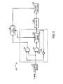
- FIG. 2 is a schematic diagram of an IR decoder circuit 50 in accordance with an exemplary embodiment of the present invention.
- the circuit 50 is part of FPGA of an electronic device, such as the FPGA 20 of electronic device 10 of FIG. 1 .
- the circuit 50 may be coupled to additional components described above with regard to the electronic device 10. Such components include the detector 16, main processor 18, relay drive 28 and power supply 30.
- the circuit 50 includes AND gates 52 and 54, an FPGA IR decoder 56 and an inverter 58.
- the AND gates 52 and 54 are coupled in parallel to the detector 16.
- the AND gate 54 is further coupled in series to the main processor 18 and AND gate 52 is further coupled in series to the FPGA IR decoder 56.
- the FPGA IR decoder 56 is coupled in parallel to the relay drive 28 and to the main processor 18.
- an inverter 58 is coupled between FPGA IR decoder 56/relay drive 28 and the AND gate 54.
- the relay drive 28 is coupled to the power supply 30 which, in turn is coupled to the main processor 18.
- the circuit 50 splits IR decoding functionality between the FPGA 20 and the main processor 18.
- the device 10 when the device 10 is switched off, it is set to a low power mode in which only the circuit 50 may be operable within electronic device 10.
- the circuit 50 maintains the relay drive in an "off" state such that the main processor 18 and systems 22-26 ( FIG. 1 ) are disconnected from the power supply 30.
- incoming IR signals are intercepted by the detector 16 and are routed to gates 52 and 54. Because the main processor is disconnected from the power supply 30 when the circuit 50 is placed in the "off" state, all incoming IR signals 14 are processed by the gate 52 and, thereafter, by the FPGA IR decoder 56.
- Further processing of the incoming IR signals 14 entails parsing those signals into what are known as a "preamble” portion and a "command” portion, where each portion typically comprises a certain number of bits, such as 12, 24, etc.
- the FPGA IR decoder 56 is adapted to compare the bits of the preamble and/or command of the IR signal to predefined values stored in a look-up table (LUT) included in the FPGA IR decoder 56. Such comparison determines whether bit-values of the command and/or preamble match the predefined values of the LUT which may be a precondition for changing the power mode of the circuit 50.
- LUT look-up table
- a matching between the "command" and the predefined value stored on the LUT of the FPGA IR decoder 56 produces a signal switching the relay drive 28 to an "on” state, whereby the power supply 30 powers the main processor 18 so that it may be fully operational.
- the relay drive remains in an "off” state.
- a matching of the "preamble" to a LUT stored on the FPGA IR decoder 56 produces a signal that is routed, via inverter 58, to gate 54 to be further processed by the main processor 18.
- the electronic device operates at a full power mode in which the main processor 18 takes full control over IR decoding, while the circuit 50 is idle.
- the relay drive 28 may be set to an “off” state, thereby disconnecting the power supply 30 from the main processor 18 and activating circuit 50.
- FIG. 3 is a flow chart 70 of a method of operation of an IR decoder in accordance with an exemplary embodiment of the present invention.
- the method 70 provides steps in which functionality of IR decoding is split between the device's main processor 18 and FPGA's 20.
- the method 70 may be implemented by the IR decoding circuit 50 of the electronic device 10 described above with reference to FIGS. 1 and 2 .
- the method begins at block 71. Thereafter, the method proceeds to block 72 in which IR signals encoded with certain commands and/or functions are received by an IR decoder. Such IR signals are then forwarded to an IR decoding circuit, such as circuit 50 ( FIG. 2 ), for further processing.
- decision junction 74 determines whether to forward incoming I R signals to the main processor (e.g., 18, FIG. 2 ) of the electronic device or to the FPGA IR decoder (e.g., 56, FIG. 2 ) of the IR decoding circuit 50. For example, when the electronic device operates in a low power mode, incoming I R signals are forwarded and compared to an LUT stored on the FPGA IR decoder. However, when the electronic device (e.g., 10 FIG. 1 ) is turned on, the electronic device is placed in a high power mode and the logic level of the FPGA IR decoding circuit changes such that it becomes idle. Consequently, the main processor of the electronic device acquires all IR decoding functionalities. In this situation, all incoming IR signals are forwarded to the main processor of the electronic device and subsequent main processor IR decoding is implemented.
- the main processor e.g. 18, FIG. 2
- FPGA IR decoder e.g., 56, FIG. 2
- the method proceeds to block 76 in which the IR signals are provided to an FPGA IR decoder (e.g., 56, FIG. 2 ). Accordingly, at block 76 IR signals are decoded and compared by the FPGA IR decoder to existing values stored on the LUT. However, if the power mode is high, meaning the electronic device (e.g., 10, FIG. 1 ) is turned on the method 70 proceeds to block 78 in which all incoming IR signals are directed to the main processor so that it may decode all incoming IR signals.
- FPGA IR decoder e.g., 56, FIG. 2
- incoming IR signals are parsed, in part, into a "preamble” portion and a "command” portion, such that each of those portions are represented by certain number of bits.
- These portions of the IR signal may then be compared to predefined values stored in a look-up table (LUT). Such a comparison may determine whether the aforementioned portions of the IR signal produces an output signal changing the power mode of the IR decoding circuit. Accordingly, from block 76 the method 70 proceeds to decision junction 80 to determine whether, for example, the "command" portion of the IR signal matches the predefined value stored in the LUT. If so, the method proceeds to block 82 in which a relay drive, such as the relay drive 28 ( FIG.
- the method 70 proceeds to block 84 and the main processor acquires all IR decoding functionalities.
- the method 70 proceeds to decision junction 86 to determine the nature of the command contained within a received IR signal. If the received IR signal fails to include an "off" command, that is, a command switching the electronic device from a high power mode to a low power mode, then the method 70 proceeds to block 88. Accordingly, at block 88 IR signals other than ones including an "off" command are processed by the device's main processor. From block 88 the method 70 loops back to block 72.
- the method 70 proceeds to block 90. Accordingly, at block 90 the logic level of the FPGA changes thereby switching the relay drive (e.g., relay drive 28, FIG. 2 ) to an "off" state, in which FPGA IR decoding is implemented as the electronic device is switched to low power mode.
- the relay drive e.g., relay drive 28, FIG. 2
Landscapes
- Physics & Mathematics (AREA)
- General Physics & Mathematics (AREA)
- Selective Calling Equipment (AREA)
- Power Sources (AREA)
Description
- The present invention relates to infra-red (IR) decoders used in electronic devices, such as televisions (TVs), digital versatile video recorders (DVDRs), video cassette recorders (VCRs),computers, personal digital assistants (PDAs), video cameras, cell phones and so forth.
- This section is intended to introduce the reader to various aspects of art which may be related to various aspects of the present invention which are described and/or claimed below. This discussion is believed to be helpful in providing the reader with background information to facilitate a better understanding of the various aspects of the present invention. Accordingly, it should be understood that these statements are to be read in this light, and not as admissions of prior art.
- Electronic devices, such as the devices mentioned above, may be controlled remotely by a remote device, typically known as a remote control. A remote control conveniently enables a user to access the electronic device from a distance so that the user may, for example, change settings and configurations of the electronic device otherwise requiring the user to physically access the electronic device. Controlling the electronic device from a distance is achieved by transmission of IR burst/signals from the remote control to the electronic device. Such IR bursts contain encoded information corresponding to commands and/or functions prompting the electronic device, from a distance, to execute user-desired functionalities. Upon reception by the electronic device, the IR signals transmitted by the remote control undergo processing by dedicated circuitry and/or software disposed within the electronic device so as to decode the information contained in the IR signals. Thereafter, the decoded information may be forwarded to a main processor of the electronic device so that the commands and/or functions may be executed accordingly.
- Hardware and/or software components used in implementing IR decoders, such as in TVs, DVDRs, etc., are powered by a main power supply disposed within such aforementioned devices. Particularly, during periods of time when the electronic device is turned off, the IR decoder may remain powered so that it can switch the electronic device back on when prompted by the remote control operated by the user. Further, known electronic devices may power the IR decoder contained therein during periods of time when the electronic device is not operating with the same amount of power otherwise used for powering the device when it is fully operating. Consequently, in such periods of time, which can be long, the IR decoder may consume large amounts of electrical power while the electronic device is turned off. As a result, the IR decoders may unnecessarily consume electrical power, further rendering such electronic devices non-compliant with various industry standards requiring low consumption of power by IR decoders when the electronic device does not operate.
-
EP 1111754 describes a remote control receiver and a method of controlling the same. -
JP 2005-295289 -
US 2005/093374 describes a power control circuit operable to connect and disconnect a power source from a circuit. -
US 2006/012489 describes an appliance control apparatus and electrical applicance. - The disclosed embodiments relate to an electronic device configured to receive infra red (IR) signals, comprising a first IR decoder configured to decode the IR signals when the electronic device is operating in a first power mode, wherein the first power mode includes the electronic device being connected to a first power supply and receiving power from the first power supply; and a second IR decoder configured to decode the IR signals when the electronic device is operating in a second power mode, wherein the second power mode includes: the electronic device not receiving power from the first power supply; and the second IR decoder receiving power from a second power supply.
- In the drawings:
-
FIG. 1 is a schematic diagram of a remotely operated electronic device in accordance with an exemplary embodiment of the present invention; -
FIG. 2 is schematic diagram of an IR decoder circuit in accordance with an exemplary embodiment of the present invention; and -
FIG. 3 is a flow chart of a method of operation of an IR decoder in accordance with an exemplary embodiment of the present invention. - One or more specific embodiments of the present invention will be described below. In an effort to provide a concise description of these embodiments, not all features of an actual implementation are described in the specification. It should be appreciated that in the development of any such actual implementation, as in any engineering or design project, numerous implementation-specific decisions must be made to achieve the developers' specific goals, such as compliance with system-related and business-related constraints, which may vary from one implementation to another. Moreover, it should be appreciated that such a development effort might be complex and time consuming, but would nevertheless be a routine undertaking of design, fabrication, and manufacture for those of ordinary skill having the benefit of this disclosure.
-
FIG. 1 is a schematic diagram of a remotely operatedelectronic device 10 in accordance with an exemplary embodiment of the present invention. Theelectronic device 10 may be a TV, computer, DVDR, VCR, PDA, video cameras, cell phone or the like. Thedevice 10 is controlled by aremote device 12, such as a remote control, configured to transmitI R signals 14 to theelectronic device 10. TheIR signals 14 emitted by theremote control 12 encode various operational commands and functions enabling, for example, a user to switch thedevice 10 on and off, change the channels of thedevice 10 and/or control other settings and features of thedevice 10, that is, features and configurations normally incorporated in the previously mentioned electronic devices. - As further depicted in
FIG. 1 , theelectronic device 10 is formed of various circuits and devices adapted to intercept, process and execute incoming IR signals emitted by theremote control 12. Accordingly, theelectronic device 10 is formed of anoptical detector 16, such as a photodetector, adapted to receive theIR signals 14 and convert such optical signals into electrical signals so that these may be forwarded for processing by additional hardware of theelectronic device 10. Theelectronic device 10 further includes amain processor 18 and field programmable gate arrays (FPGA) 20, both of which may be connected to thedetector 16. Themain processor 18 may be coupled to other systems included in theelectronic device 10, includingdisplay systems 22,sound systems 24 andcontrol systems 26. When theelectronic device 10 is fully operational, i.e., turned on, themain processor 18 receives and processes encoded IR commands which control the systems 22-26. For example, where theelectronic device 10 is a TV,main processor 18 may process certain commands received from theremote control 12 to control the TV's brightness and/or sound pitch as provided by the display andsound systems main processor 18 may process rewind and forward commands received by theremote control 12 to prompt thecontrol system 26 for operating the rewinding/forwarding wheel of the VCR accordingly. - The
FPGA 20 are formed of programmable logic blocks and programmable interconnects typically formed of semiconductor devices. TheFPGA 20 may be programmable to emulate the functionality of basic logic gates such as AND, OR, XOR, NOT or more complex combinational functions such as decoders or math functions. TheFPGA 20 may also include memory elements, which may be simple flip-flops or complete blocks of memories. In the illustrated embodiment,main processor 18 andFPGA 20 are adapted to implement an IR decoder whose functionality is split between themain processor 18 and theFPGA 20 when the electronic device is turned on/off, respectively. Such an implementation of an I R decoder enables theelectronic device 10 to consume low amounts of power while it is turned off. While in the illustrated embodiment theFPGA 20 are shown as a separate component frommain processor 18, other embodiments may haveFPGA 20 incorporated with the main processor of the device. It should further be noted that theFPGA 20 may be adapted to perform numerous operations, many of which may be active during periods of time when the electronic device is turned on and, some of which may be unrelated to the operation of the present IR decoder. - The
FPGA 20 are coupled to apermanent power supply 21 configured to supply constant power to theFPGA 20 during their operation. During periods of time in which thedevice 10 is turned off and low power mode FPGA IR decoding is enabled,permanent power supply 21 provides the low but sufficient power to those components of theFPGA 20 implementing IR decoding. When thedevice 10 is turned on,switchable power supply 30 may provide additional power to theFPGA 20 to enable their complete operation. - The
electronic device 10 further includes arelay drive 28 connected to theFPGA 20 and to aswitchable power supply 30. The swithcablepower supply 30 is connected to themain processor 18. During periods of time in which theelectronic device 10 is turned on, theswitchable power supply 30 is configured to supply power to themain processor 18, as well as to other systems contained within theelectronic device 10, such as thesystems 20 and 22-26. Similarly, during periods of time when theelectronic device 10 is off, no power is delivered to themain processor 18 and to the systems 22-26 as thepower supply 30 is disconnected from those components. Such switching capabilities ofpower supply 30 are controlled by therelay drive 28. - The components of the
electronic device 10, as described above, form an IR decoder whose function is split between theFPGA 20 and themain processor 18. Such a splitting occurs as thedevice 10 transitions between on/off states. For example, whendevice 10 is switched off remotely, theremote control 12 emits theIR signals 14 which are intercepted by thedetector 16 and are forwarded as electrical signals to themain processor 18 and to theFPGA 20. Such IR signals encode a command disconnecting themain processor 18 and systems 22-26 from thepower supply 30 while powering portions of theFPGA 20 configured to function as the IR decoder when theelectronic device 10 is switched off. Accordingly, circuit blocks within theFPGA 20 designated for IR decoding are adapted to consume low amounts of power such that the overall consumption of power by theelectronic device 10, when switched off, is low as well. As a result, such a configuration may render theelectronic device 10 complaint with present industry standards, one of which is known as "Energy Star," an industry standard requiring electronic devices employing IR decoders to consume low amounts of power. - Similarly, when the
electronic device 10 is switched on, theremote control 12 emits IR signals 14 encoding commands and/or functions enabling therelay drive 28 to connect thepower supply 30 to themain processor 18, while providing additional power to theFPGA 20. At that instant, themain processor 18 takes over all IR decoding functionalities for decoding most commands and/or functions received from theremote control 12 when theelectronic device 10 is switched on. It should be born in mind that implementing FPGA IR decoding, as described below inFIG. 2 , requires no additional hardware and/or software on top of what is normally included in electronic devices, such as those mentioned above. Thus, to the extent existing FPGA (e.g., FPGA 20) of an electronic device (e.g., electronic device 10) are configurable for IR decoding, the present technique does not require any additional components to be added to theelectronic device 10 that normally would not be included in such a device. -
FIG. 2 is a schematic diagram of anIR decoder circuit 50 in accordance with an exemplary embodiment of the present invention. In the illustrated embodiment thecircuit 50 is part of FPGA of an electronic device, such as theFPGA 20 ofelectronic device 10 ofFIG. 1 . As further depicted byFIG. 2 , thecircuit 50 may be coupled to additional components described above with regard to theelectronic device 10. Such components include thedetector 16,main processor 18,relay drive 28 andpower supply 30. - Generally, the
circuit 50 includes ANDgates FPGA IR decoder 56 and aninverter 58. The ANDgates detector 16. The ANDgate 54 is further coupled in series to themain processor 18 and ANDgate 52 is further coupled in series to theFPGA IR decoder 56. TheFPGA IR decoder 56 is coupled in parallel to therelay drive 28 and to themain processor 18. Further, aninverter 58 is coupled betweenFPGA IR decoder 56/relay drive 28 and the ANDgate 54. Therelay drive 28 is coupled to thepower supply 30 which, in turn is coupled to themain processor 18. - Hence, when implemented in an electronic device, such as the
electronic device 10 ofFIG. 1 , thecircuit 50 splits IR decoding functionality between theFPGA 20 and themain processor 18. In accordance with the present technique, when thedevice 10 is switched off, it is set to a low power mode in which only thecircuit 50 may be operable withinelectronic device 10. In such a mode, thecircuit 50 maintains the relay drive in an "off" state such that themain processor 18 and systems 22-26 (FIG. 1 ) are disconnected from thepower supply 30. As a result, incoming IR signals are intercepted by thedetector 16 and are routed togates power supply 30 when thecircuit 50 is placed in the "off" state, all incoming IR signals 14 are processed by thegate 52 and, thereafter, by theFPGA IR decoder 56. - Further processing of the incoming IR signals 14 entails parsing those signals into what are known as a "preamble" portion and a "command" portion, where each portion typically comprises a certain number of bits, such as 12, 24, etc. The
FPGA IR decoder 56 is adapted to compare the bits of the preamble and/or command of the IR signal to predefined values stored in a look-up table (LUT) included in theFPGA IR decoder 56. Such comparison determines whether bit-values of the command and/or preamble match the predefined values of the LUT which may be a precondition for changing the power mode of thecircuit 50. For example, a matching between the "command" and the predefined value stored on the LUT of theFPGA IR decoder 56 produces a signal switching therelay drive 28 to an "on" state, whereby thepower supply 30 powers themain processor 18 so that it may be fully operational. However, if no matching exists between the "command" and the LUT, the relay drive remains in an "off" state. - By the same token, a matching of the "preamble" to a LUT stored on the
FPGA IR decoder 56 produces a signal that is routed, viainverter 58, togate 54 to be further processed by themain processor 18. At this point, the electronic device operates at a full power mode in which themain processor 18 takes full control over IR decoding, while thecircuit 50 is idle. When theelectronic device 10 is turned off, as dictated by a certain "command" and/or a "preamble" processed by themain processor 18, therelay drive 28 may be set to an "off" state, thereby disconnecting thepower supply 30 from themain processor 18 and activatingcircuit 50. -
FIG. 3 is aflow chart 70 of a method of operation of an IR decoder in accordance with an exemplary embodiment of the present invention. Themethod 70 provides steps in which functionality of IR decoding is split between the device'smain processor 18 and FPGA's 20. Thus, themethod 70 may be implemented by theIR decoding circuit 50 of theelectronic device 10 described above with reference toFIGS. 1 and2 . The method begins atblock 71. Thereafter, the method proceeds to block 72 in which IR signals encoded with certain commands and/or functions are received by an IR decoder. Such IR signals are then forwarded to an IR decoding circuit, such as circuit 50 (FIG. 2 ), for further processing. - Accordingly, the
method 70 proceeds todecision junction 74, whereby the power mode of the electronic device is determined. Stated otherwise,decision junction 74 determines whether to forward incoming I R signals to the main processor (e.g., 18,FIG. 2 ) of the electronic device or to the FPGA IR decoder (e.g., 56,FIG. 2 ) of theIR decoding circuit 50. For example, when the electronic device operates in a low power mode, incoming I R signals are forwarded and compared to an LUT stored on the FPGA IR decoder. However, when the electronic device (e.g., 10FIG. 1 ) is turned on, the electronic device is placed in a high power mode and the logic level of the FPGA IR decoding circuit changes such that it becomes idle. Consequently, the main processor of the electronic device acquires all IR decoding functionalities. In this situation, all incoming IR signals are forwarded to the main processor of the electronic device and subsequent main processor IR decoding is implemented. - Hence, if at
decision junction 74 it is determined that the power mode is low, the method proceeds to block 76 in which the IR signals are provided to an FPGA IR decoder (e.g., 56,FIG. 2 ). Accordingly, atblock 76 IR signals are decoded and compared by the FPGA IR decoder to existing values stored on the LUT. However, if the power mode is high, meaning the electronic device (e.g., 10,FIG. 1 ) is turned on themethod 70 proceeds to block 78 in which all incoming IR signals are directed to the main processor so that it may decode all incoming IR signals. - Returning to block 76, incoming IR signals are parsed, in part, into a "preamble" portion and a "command" portion, such that each of those portions are represented by certain number of bits. These portions of the IR signal may then be compared to predefined values stored in a look-up table (LUT). Such a comparison may determine whether the aforementioned portions of the IR signal produces an output signal changing the power mode of the IR decoding circuit. Accordingly, from
block 76 themethod 70 proceeds todecision junction 80 to determine whether, for example, the "command" portion of the IR signal matches the predefined value stored in the LUT. If so, the method proceeds to block 82 in which a relay drive, such as the relay drive 28 (FIG. 2 ), is set to an on state and main processor IR decoding is implemented. However, if no matching exists between the "command" portion of the IR signal and the predefined value stored on the LUT of the comparator, the logic level of the FPGA IR decoding circuit remains unchanged and the FPGA IR decoding remains implemented. - Returning to block 78 where the electronic device operates in high power mode, the
method 70 proceeds to block 84 and the main processor acquires all IR decoding functionalities. Thus, upon reception of further IR signals, themethod 70 proceeds todecision junction 86 to determine the nature of the command contained within a received IR signal. If the received IR signal fails to include an "off" command, that is, a command switching the electronic device from a high power mode to a low power mode, then themethod 70 proceeds to block 88. Accordingly, atblock 88 IR signals other than ones including an "off" command are processed by the device's main processor. Fromblock 88 themethod 70 loops back to block 72. - However, if at
decision junction 86 it is determined that the received IR signal contains an "off" command, themethod 70 proceeds to block 90. Accordingly, atblock 90 the logic level of the FPGA changes thereby switching the relay drive (e.g.,relay drive 28,FIG. 2 ) to an "off" state, in which FPGA IR decoding is implemented as the electronic device is switched to low power mode. - While the invention may be susceptible to various modifications and alternative forms, specific embodiments have been shown by way of example in the drawings and will be described in detail herein. However, it should be understood that the invention is not intended to be limited to the particular forms disclosed. Rather, the invention is to cover all modifications, equivalents and alternatives falling within the scope of the invention as defined by the following appended claims.
Claims (12)
- An electronic device (10) configured to receive infra-red (IR) signals (14), comprising:a first IR decoder (18) configured to decode the IR signals (14) when the electronic device (10) is operating in a first power mode, wherein the first power mode includes the electronic device (10) being connected to a first power supply (30) and receiving power from the first power supply; anda second IR decoder (20) configured to decode the IR signals (14) when the electronic device (10) is operating in a second power mode, wherein the second power mode includes:the electronic device (10) not receiving power from the first power supply (30); andthe second IR decoder (20) receiving power from a second power supply (21).
- The electronic device (10) of claim 1, wherein the electronic device (10) comprises a television (TV), a digital versatile video recorder (DVDR), a computer, a video cassette recorder (VCR), a video camera, a personal digital assistant (PDA), or a cell phone.
- The electronic device (10) of claim 1, wherein the first IR decoder (18) comprises a computer processing unit and the second IR decoder (20) comprises a field programmable gate array (FPGA).
- The electronic device (10) of claim 1, wherein the second power mode is a low power mode compliant with an "Energy Star" industry standard.
- The electronic device (10) of claim 1, wherein the second IR decoder (20) comprises an FPGA IR decoder (56) coupled to a relay drive (28), wherein the relay drive (28) is configured to switch the electronic device (10) between the first power mode and the second power mode.
- The electronic device (10) of claim 5, wherein the FPGA IR decoder (56) is configured to compare portions of the IR signal (14) to predefined values stored in a look-up table (LUT) to determine whether to switch the electronic device (10) from the second power mode to the first power mode.
- The electronic device (10) of claim 1, wherein the first power mode corresponds to a first logic level of the second IR decoder (20) and the second power mode corresponds to a second logic level of the second IR decoder.
- The electronic device (10) of claim 1, wherein the first power supply (30) is a switchable power supply and the second power supply (21) is a permanent power supply.
- A method (70) for processing infra-red (IR) signals (14) of an electronic device (10) comprising a first IR decoding circuit (18), a second IR decoding circuit (20), a first power supply (30) and a second power supply (21), wherein the electronic device (10) is configured to operate in a first power mode in which the electronic device (10) is connected to the first power supply (30) and receives power from the first power supply (30), and in a second power mode in which the electronic device (10) does not receive power from the first power supply (30) and the second IR decoding circuit (20) receives power from the second power supply (21), the method comprising:receiving (72) an infra-red signal comprising a plurality of bits;determining a logic level of the second IR decoding circuit;if the logic level of the second IR decoding circuit is set to a first level, comparing (76) values of the bits to predefined values stored in a look-up table (LUT), wherein the first level corresponds to the second power modechanging (82) the power mode to the first power mode, including changing the logic level of the second IR decoding circuit (20), if the values of the bits comprising the IR signal match the predefined values; androuting (78) the IR signal to the first IR decoding circuit if the logic level of the second IR decoding circuit is different from the first level corresponding to the second power mode.
- The method (70) of claim 9, wherein the IR signal comprises a command portion and a preamble portion.
- The method (70) of claim 10, comprising changing (82) the logic level of the first IR decoding circuit only if values of the bits of the command portion of the IR signal match predefined command values.
- The method (70) of claim 9, wherein the first power supply (30) is a switchable power supply and the second power supply (21) is a permanent power supply.
Applications Claiming Priority (2)
| Application Number | Priority Date | Filing Date | Title |
|---|---|---|---|
| US11/708,894 US8068738B2 (en) | 2007-02-21 | 2007-02-21 | System and method for decoding infra-red (IR) signals |
| PCT/US2008/054435 WO2008103739A1 (en) | 2007-02-21 | 2008-02-20 | System and method for decoding infra-red (ir) signals |
Publications (3)
| Publication Number | Publication Date |
|---|---|
| EP2123103A1 EP2123103A1 (en) | 2009-11-25 |
| EP2123103A4 EP2123103A4 (en) | 2013-01-09 |
| EP2123103B1 true EP2123103B1 (en) | 2014-11-12 |
Family
ID=39706306
Family Applications (1)
| Application Number | Title | Priority Date | Filing Date |
|---|---|---|---|
| EP08730272.5A Not-in-force EP2123103B1 (en) | 2007-02-21 | 2008-02-20 | System and method for decoding infra-red (ir) signals |
Country Status (4)
| Country | Link |
|---|---|
| US (1) | US8068738B2 (en) |
| EP (1) | EP2123103B1 (en) |
| CN (1) | CN101658047B (en) |
| WO (1) | WO2008103739A1 (en) |
Families Citing this family (8)
| Publication number | Priority date | Publication date | Assignee | Title |
|---|---|---|---|---|
| CN101335512A (en) * | 2007-06-28 | 2008-12-31 | 深圳Tcl新技术有限公司 | Electronic device with standby function |
| US20110001887A1 (en) * | 2009-07-02 | 2011-01-06 | Peter Rae Shintani | Zero standby power RF controlled device |
| EP2483264A1 (en) * | 2009-10-01 | 2012-08-08 | Novartis AG | Pyrazole derivatives which modulate stearoyl-coa desaturase |
| TW201142648A (en) * | 2010-05-31 | 2011-12-01 | Hon Hai Prec Ind Co Ltd | Infrared controlling apparatus and infrared controlling system using the same |
| CN102270384A (en) * | 2010-06-01 | 2011-12-07 | 鸿富锦精密工业(深圳)有限公司 | Infrared control apparatus and infrared control system by using infrared control apparatus |
| US20140105273A1 (en) * | 2012-10-15 | 2014-04-17 | Broadcom Corporation | Adaptive power management within media delivery system |
| US10171110B1 (en) * | 2017-07-03 | 2019-01-01 | Seagate Technology Llc | Sequential power transitioning of multiple data decoders |
| CN108600808A (en) * | 2018-04-24 | 2018-09-28 | 青岛海信电器股份有限公司 | Signal processing method and device, television set |
Family Cites Families (15)
| Publication number | Priority date | Publication date | Assignee | Title |
|---|---|---|---|---|
| TW391588U (en) | 1998-06-19 | 2000-05-21 | Hu Yu Min | Power-saving Infra Red signal sensing system |
| JP2000300851A (en) * | 1999-02-16 | 2000-10-31 | Konami Co Ltd | Game system, game device usable in the same and storage medium readable by computer |
| US6810216B1 (en) | 1999-07-02 | 2004-10-26 | Nokia Corporation | Fast infrared transceiver with reduced power consumption |
| JP3604982B2 (en) * | 1999-12-21 | 2004-12-22 | Necマイクロシステム株式会社 | Remote control control method and device |
| JP2002026812A (en) | 2000-07-05 | 2002-01-25 | Sharp Corp | Power control device, remote control receiving device, and optical communication device |
| KR100376131B1 (en) | 2000-09-22 | 2003-03-15 | 삼성전자주식회사 | Consumption power saving apparatus and controlling method in a stand-by mode |
| US6944402B1 (en) * | 2000-11-18 | 2005-09-13 | Tribeam Technologies, Inc. | Extended range infrared communication (ERIC) for an infrared associated (IrDA) compliant portable device |
| JP2003125312A (en) | 2001-10-11 | 2003-04-25 | Sharp Corp | Standby power consumption controller |
| EP1341380A1 (en) | 2002-02-27 | 2003-09-03 | Koninklijke Philips Electronics N.V. | Power standby mode circuitry for audiovisual device |
| US6914527B2 (en) | 2003-04-29 | 2005-07-05 | Jui-Hung Hsu | Infrared detector |
| US7250695B2 (en) * | 2003-10-31 | 2007-07-31 | Hewlett-Packard Development Company, L.P. | Controlling power supplied to a circuit using an externally applied magnetic field |
| JP2005295289A (en) | 2004-04-01 | 2005-10-20 | Yamaha Corp | Remote controller and electric appiance |
| JP2006025069A (en) * | 2004-07-07 | 2006-01-26 | Hitachi Ltd | Device control device and electrical device |
| US7840142B2 (en) | 2004-07-23 | 2010-11-23 | Thomson Licensing | System and method for reducing standby power consumption |
| KR20060059655A (en) | 2004-11-29 | 2006-06-02 | 엘지전자 주식회사 | Low Power Control Circuit of Infrared Data Receiver |
-
2007
- 2007-02-21 US US11/708,894 patent/US8068738B2/en not_active Expired - Fee Related
-
2008
- 2008-02-20 WO PCT/US2008/054435 patent/WO2008103739A1/en not_active Ceased
- 2008-02-20 EP EP08730272.5A patent/EP2123103B1/en not_active Not-in-force
- 2008-02-20 CN CN2008800050395A patent/CN101658047B/en not_active Expired - Fee Related
Also Published As
| Publication number | Publication date |
|---|---|
| EP2123103A1 (en) | 2009-11-25 |
| CN101658047B (en) | 2012-05-02 |
| EP2123103A4 (en) | 2013-01-09 |
| CN101658047A (en) | 2010-02-24 |
| US8068738B2 (en) | 2011-11-29 |
| WO2008103739A1 (en) | 2008-08-28 |
| US20080198273A1 (en) | 2008-08-21 |
Similar Documents
| Publication | Publication Date | Title |
|---|---|---|
| US8068738B2 (en) | System and method for decoding infra-red (IR) signals | |
| US7768421B2 (en) | Control signal receiving apparatus | |
| US20090092397A1 (en) | Wireless remote control device, bridge device and wireless remote control system | |
| KR20040079474A (en) | Home gateway system with power management function | |
| US9210356B2 (en) | System and method for entertainment system reconfiguration | |
| US7138928B2 (en) | Method and apparatus for positive control of devices with toggle power control | |
| US20070268403A1 (en) | Power Saving Control Device and Method | |
| KR100403096B1 (en) | Remote control receiver and method of controlling the same | |
| US20100117853A1 (en) | Infra-red (ir) decoding circuit | |
| EP2513883B1 (en) | Method and apparatus for controlling an electronic system | |
| US7647442B2 (en) | Series-connected control system | |
| US20100162017A1 (en) | Systems and methods for implementing standby functionality using field programmable gate arrays | |
| US9270330B2 (en) | Radio communication system and method | |
| JP2003179985A (en) | Remote control signal transmission method | |
| US20070106802A1 (en) | Reproduction system and server | |
| US9274995B2 (en) | Electronic apparatus | |
| KR100508596B1 (en) | A display device having function for controlling power on/off in connected image devices and method thereof | |
| KR100227737B1 (en) | Method for detecting remote control signal | |
| JP2009100269A (en) | Remote control transmitter and control method of audio equipment | |
| JP2011040930A (en) | Electronic device | |
| KR20050078317A (en) | Method and apparatus of controlling power for display | |
| JP2005328174A (en) | Remote control unit | |
| KR20070065533A (en) | Digital audio / video device operation control method | |
| JP2006332926A (en) | Electrical equipment and power supply control method | |
| JP2008072532A (en) | Semiconductor integrated circuit device |
Legal Events
| Date | Code | Title | Description |
|---|---|---|---|
| PUAI | Public reference made under article 153(3) epc to a published international application that has entered the european phase |
Free format text: ORIGINAL CODE: 0009012 |
|
| 17P | Request for examination filed |
Effective date: 20090810 |
|
| AK | Designated contracting states |
Kind code of ref document: A1 Designated state(s): AT BE BG CH CY CZ DE DK EE ES FI FR GB GR HR HU IE IS IT LI LT LU LV MC MT NL NO PL PT RO SE SI SK TR |
|
| DAX | Request for extension of the european patent (deleted) | ||
| A4 | Supplementary search report drawn up and despatched |
Effective date: 20121206 |
|
| RIC1 | Information provided on ipc code assigned before grant |
Ipc: G08C 23/04 20060101ALI20121130BHEP Ipc: H04Q 9/00 20060101AFI20121130BHEP |
|
| GRAP | Despatch of communication of intention to grant a patent |
Free format text: ORIGINAL CODE: EPIDOSNIGR1 |
|
| INTG | Intention to grant announced |
Effective date: 20140704 |
|
| GRAS | Grant fee paid |
Free format text: ORIGINAL CODE: EPIDOSNIGR3 |
|
| GRAA | (expected) grant |
Free format text: ORIGINAL CODE: 0009210 |
|
| AK | Designated contracting states |
Kind code of ref document: B1 Designated state(s): AT BE BG CH CY CZ DE DK EE ES FI FR GB GR HR HU IE IS IT LI LT LU LV MC MT NL NO PL PT RO SE SI SK TR |
|
| REG | Reference to a national code |
Ref country code: GB Ref legal event code: FG4D |
|
| REG | Reference to a national code |
Ref country code: CH Ref legal event code: EP |
|
| REG | Reference to a national code |
Ref country code: AT Ref legal event code: REF Ref document number: 696375 Country of ref document: AT Kind code of ref document: T Effective date: 20141115 |
|
| REG | Reference to a national code |
Ref country code: IE Ref legal event code: FG4D |
|
| REG | Reference to a national code |
Ref country code: DE Ref legal event code: R096 Ref document number: 602008035304 Country of ref document: DE Effective date: 20141224 |
|
| REG | Reference to a national code |
Ref country code: NL Ref legal event code: VDEP Effective date: 20141112 |
|
| REG | Reference to a national code |
Ref country code: AT Ref legal event code: MK05 Ref document number: 696375 Country of ref document: AT Kind code of ref document: T Effective date: 20141112 |
|
| PG25 | Lapsed in a contracting state [announced via postgrant information from national office to epo] |
Ref country code: IS Free format text: LAPSE BECAUSE OF FAILURE TO SUBMIT A TRANSLATION OF THE DESCRIPTION OR TO PAY THE FEE WITHIN THE PRESCRIBED TIME-LIMIT Effective date: 20150312 Ref country code: LT Free format text: LAPSE BECAUSE OF FAILURE TO SUBMIT A TRANSLATION OF THE DESCRIPTION OR TO PAY THE FEE WITHIN THE PRESCRIBED TIME-LIMIT Effective date: 20141112 Ref country code: ES Free format text: LAPSE BECAUSE OF FAILURE TO SUBMIT A TRANSLATION OF THE DESCRIPTION OR TO PAY THE FEE WITHIN THE PRESCRIBED TIME-LIMIT Effective date: 20141112 Ref country code: FI Free format text: LAPSE BECAUSE OF FAILURE TO SUBMIT A TRANSLATION OF THE DESCRIPTION OR TO PAY THE FEE WITHIN THE PRESCRIBED TIME-LIMIT Effective date: 20141112 Ref country code: NO Free format text: LAPSE BECAUSE OF FAILURE TO SUBMIT A TRANSLATION OF THE DESCRIPTION OR TO PAY THE FEE WITHIN THE PRESCRIBED TIME-LIMIT Effective date: 20150212 Ref country code: PT Free format text: LAPSE BECAUSE OF FAILURE TO SUBMIT A TRANSLATION OF THE DESCRIPTION OR TO PAY THE FEE WITHIN THE PRESCRIBED TIME-LIMIT Effective date: 20150312 Ref country code: NL Free format text: LAPSE BECAUSE OF FAILURE TO SUBMIT A TRANSLATION OF THE DESCRIPTION OR TO PAY THE FEE WITHIN THE PRESCRIBED TIME-LIMIT Effective date: 20141112 |
|
| PG25 | Lapsed in a contracting state [announced via postgrant information from national office to epo] |
Ref country code: AT Free format text: LAPSE BECAUSE OF FAILURE TO SUBMIT A TRANSLATION OF THE DESCRIPTION OR TO PAY THE FEE WITHIN THE PRESCRIBED TIME-LIMIT Effective date: 20141112 Ref country code: SE Free format text: LAPSE BECAUSE OF FAILURE TO SUBMIT A TRANSLATION OF THE DESCRIPTION OR TO PAY THE FEE WITHIN THE PRESCRIBED TIME-LIMIT Effective date: 20141112 Ref country code: CY Free format text: LAPSE BECAUSE OF FAILURE TO SUBMIT A TRANSLATION OF THE DESCRIPTION OR TO PAY THE FEE WITHIN THE PRESCRIBED TIME-LIMIT Effective date: 20141112 Ref country code: GR Free format text: LAPSE BECAUSE OF FAILURE TO SUBMIT A TRANSLATION OF THE DESCRIPTION OR TO PAY THE FEE WITHIN THE PRESCRIBED TIME-LIMIT Effective date: 20150213 Ref country code: LV Free format text: LAPSE BECAUSE OF FAILURE TO SUBMIT A TRANSLATION OF THE DESCRIPTION OR TO PAY THE FEE WITHIN THE PRESCRIBED TIME-LIMIT Effective date: 20141112 Ref country code: HR Free format text: LAPSE BECAUSE OF FAILURE TO SUBMIT A TRANSLATION OF THE DESCRIPTION OR TO PAY THE FEE WITHIN THE PRESCRIBED TIME-LIMIT Effective date: 20141112 Ref country code: PL Free format text: LAPSE BECAUSE OF FAILURE TO SUBMIT A TRANSLATION OF THE DESCRIPTION OR TO PAY THE FEE WITHIN THE PRESCRIBED TIME-LIMIT Effective date: 20141112 |
|
| PG25 | Lapsed in a contracting state [announced via postgrant information from national office to epo] |
Ref country code: RO Free format text: LAPSE BECAUSE OF FAILURE TO SUBMIT A TRANSLATION OF THE DESCRIPTION OR TO PAY THE FEE WITHIN THE PRESCRIBED TIME-LIMIT Effective date: 20141112 Ref country code: DK Free format text: LAPSE BECAUSE OF FAILURE TO SUBMIT A TRANSLATION OF THE DESCRIPTION OR TO PAY THE FEE WITHIN THE PRESCRIBED TIME-LIMIT Effective date: 20141112 Ref country code: SK Free format text: LAPSE BECAUSE OF FAILURE TO SUBMIT A TRANSLATION OF THE DESCRIPTION OR TO PAY THE FEE WITHIN THE PRESCRIBED TIME-LIMIT Effective date: 20141112 Ref country code: EE Free format text: LAPSE BECAUSE OF FAILURE TO SUBMIT A TRANSLATION OF THE DESCRIPTION OR TO PAY THE FEE WITHIN THE PRESCRIBED TIME-LIMIT Effective date: 20141112 Ref country code: CZ Free format text: LAPSE BECAUSE OF FAILURE TO SUBMIT A TRANSLATION OF THE DESCRIPTION OR TO PAY THE FEE WITHIN THE PRESCRIBED TIME-LIMIT Effective date: 20141112 |
|
| REG | Reference to a national code |
Ref country code: DE Ref legal event code: R097 Ref document number: 602008035304 Country of ref document: DE |
|
| PLBE | No opposition filed within time limit |
Free format text: ORIGINAL CODE: 0009261 |
|
| STAA | Information on the status of an ep patent application or granted ep patent |
Free format text: STATUS: NO OPPOSITION FILED WITHIN TIME LIMIT |
|
| PG25 | Lapsed in a contracting state [announced via postgrant information from national office to epo] |
Ref country code: LU Free format text: LAPSE BECAUSE OF FAILURE TO SUBMIT A TRANSLATION OF THE DESCRIPTION OR TO PAY THE FEE WITHIN THE PRESCRIBED TIME-LIMIT Effective date: 20150220 |
|
| REG | Reference to a national code |
Ref country code: CH Ref legal event code: PL |
|
| 26N | No opposition filed |
Effective date: 20150813 |
|
| PG25 | Lapsed in a contracting state [announced via postgrant information from national office to epo] |
Ref country code: CH Free format text: LAPSE BECAUSE OF NON-PAYMENT OF DUE FEES Effective date: 20150228 Ref country code: LI Free format text: LAPSE BECAUSE OF NON-PAYMENT OF DUE FEES Effective date: 20150228 Ref country code: MC Free format text: LAPSE BECAUSE OF FAILURE TO SUBMIT A TRANSLATION OF THE DESCRIPTION OR TO PAY THE FEE WITHIN THE PRESCRIBED TIME-LIMIT Effective date: 20141112 |
|
| REG | Reference to a national code |
Ref country code: IE Ref legal event code: MM4A |
|
| PG25 | Lapsed in a contracting state [announced via postgrant information from national office to epo] |
Ref country code: IT Free format text: LAPSE BECAUSE OF FAILURE TO SUBMIT A TRANSLATION OF THE DESCRIPTION OR TO PAY THE FEE WITHIN THE PRESCRIBED TIME-LIMIT Effective date: 20141112 |
|
| PG25 | Lapsed in a contracting state [announced via postgrant information from national office to epo] |
Ref country code: IE Free format text: LAPSE BECAUSE OF NON-PAYMENT OF DUE FEES Effective date: 20150220 |
|
| REG | Reference to a national code |
Ref country code: FR Ref legal event code: PLFP Year of fee payment: 9 |
|
| PG25 | Lapsed in a contracting state [announced via postgrant information from national office to epo] |
Ref country code: SI Free format text: LAPSE BECAUSE OF FAILURE TO SUBMIT A TRANSLATION OF THE DESCRIPTION OR TO PAY THE FEE WITHIN THE PRESCRIBED TIME-LIMIT Effective date: 20141112 |
|
| PG25 | Lapsed in a contracting state [announced via postgrant information from national office to epo] |
Ref country code: MT Free format text: LAPSE BECAUSE OF FAILURE TO SUBMIT A TRANSLATION OF THE DESCRIPTION OR TO PAY THE FEE WITHIN THE PRESCRIBED TIME-LIMIT Effective date: 20141112 |
|
| REG | Reference to a national code |
Ref country code: FR Ref legal event code: PLFP Year of fee payment: 10 |
|
| PGFP | Annual fee paid to national office [announced via postgrant information from national office to epo] |
Ref country code: DE Payment date: 20170217 Year of fee payment: 10 Ref country code: FR Payment date: 20170217 Year of fee payment: 10 |
|
| PG25 | Lapsed in a contracting state [announced via postgrant information from national office to epo] |
Ref country code: HU Free format text: LAPSE BECAUSE OF FAILURE TO SUBMIT A TRANSLATION OF THE DESCRIPTION OR TO PAY THE FEE WITHIN THE PRESCRIBED TIME-LIMIT; INVALID AB INITIO Effective date: 20080220 Ref country code: BG Free format text: LAPSE BECAUSE OF FAILURE TO SUBMIT A TRANSLATION OF THE DESCRIPTION OR TO PAY THE FEE WITHIN THE PRESCRIBED TIME-LIMIT Effective date: 20141112 |
|
| PGFP | Annual fee paid to national office [announced via postgrant information from national office to epo] |
Ref country code: GB Payment date: 20170216 Year of fee payment: 10 |
|
| PG25 | Lapsed in a contracting state [announced via postgrant information from national office to epo] |
Ref country code: TR Free format text: LAPSE BECAUSE OF FAILURE TO SUBMIT A TRANSLATION OF THE DESCRIPTION OR TO PAY THE FEE WITHIN THE PRESCRIBED TIME-LIMIT Effective date: 20141112 |
|
| PG25 | Lapsed in a contracting state [announced via postgrant information from national office to epo] |
Ref country code: BE Free format text: LAPSE BECAUSE OF FAILURE TO SUBMIT A TRANSLATION OF THE DESCRIPTION OR TO PAY THE FEE WITHIN THE PRESCRIBED TIME-LIMIT Effective date: 20141112 |
|
| REG | Reference to a national code |
Ref country code: DE Ref legal event code: R119 Ref document number: 602008035304 Country of ref document: DE |
|
| GBPC | Gb: european patent ceased through non-payment of renewal fee |
Effective date: 20180220 |
|
| REG | Reference to a national code |
Ref country code: FR Ref legal event code: ST Effective date: 20181031 |
|
| PG25 | Lapsed in a contracting state [announced via postgrant information from national office to epo] |
Ref country code: DE Free format text: LAPSE BECAUSE OF NON-PAYMENT OF DUE FEES Effective date: 20180901 |
|
| PG25 | Lapsed in a contracting state [announced via postgrant information from national office to epo] |
Ref country code: GB Free format text: LAPSE BECAUSE OF NON-PAYMENT OF DUE FEES Effective date: 20180220 Ref country code: FR Free format text: LAPSE BECAUSE OF NON-PAYMENT OF DUE FEES Effective date: 20180228 |