EP2117037A1 - Interlayer insulation film, interconnect structure, and methods for production thereof - Google Patents
Interlayer insulation film, interconnect structure, and methods for production thereof Download PDFInfo
- Publication number
- EP2117037A1 EP2117037A1 EP08711851A EP08711851A EP2117037A1 EP 2117037 A1 EP2117037 A1 EP 2117037A1 EP 08711851 A EP08711851 A EP 08711851A EP 08711851 A EP08711851 A EP 08711851A EP 2117037 A1 EP2117037 A1 EP 2117037A1
- Authority
- EP
- European Patent Office
- Prior art keywords
- atoms
- gas
- layer containing
- hydrocarbon layer
- interconnect structure
- Prior art date
- Legal status (The legal status is an assumption and is not a legal conclusion. Google has not performed a legal analysis and makes no representation as to the accuracy of the status listed.)
- Granted
Links
Images



Classifications
-
- H—ELECTRICITY
- H10—SEMICONDUCTOR DEVICES; ELECTRIC SOLID-STATE DEVICES NOT OTHERWISE PROVIDED FOR
- H10P—GENERIC PROCESSES OR APPARATUS FOR THE MANUFACTURE OR TREATMENT OF DEVICES COVERED BY CLASS H10
- H10P14/00—Formation of materials, e.g. in the shape of layers or pillars
- H10P14/60—Formation of materials, e.g. in the shape of layers or pillars of insulating materials
- H10P14/69—Inorganic materials
- H10P14/6902—Inorganic materials composed of carbon, e.g. alpha-C, diamond or hydrogen doped carbon
-
- H—ELECTRICITY
- H10—SEMICONDUCTOR DEVICES; ELECTRIC SOLID-STATE DEVICES NOT OTHERWISE PROVIDED FOR
- H10P—GENERIC PROCESSES OR APPARATUS FOR THE MANUFACTURE OR TREATMENT OF DEVICES COVERED BY CLASS H10
- H10P14/00—Formation of materials, e.g. in the shape of layers or pillars
- H10P14/60—Formation of materials, e.g. in the shape of layers or pillars of insulating materials
- H10P14/66—Formation of materials, e.g. in the shape of layers or pillars of insulating materials characterised by the type of materials
- H10P14/662—Laminate layers, e.g. stacks of alternating high-k metal oxides
-
- H—ELECTRICITY
- H10—SEMICONDUCTOR DEVICES; ELECTRIC SOLID-STATE DEVICES NOT OTHERWISE PROVIDED FOR
- H10W—GENERIC PACKAGES, INTERCONNECTIONS, CONNECTORS OR OTHER CONSTRUCTIONAL DETAILS OF DEVICES COVERED BY CLASS H10
- H10W20/00—Interconnections in chips, wafers or substrates
- H10W20/01—Manufacture or treatment
- H10W20/071—Manufacture or treatment of dielectric parts thereof
-
- H—ELECTRICITY
- H10—SEMICONDUCTOR DEVICES; ELECTRIC SOLID-STATE DEVICES NOT OTHERWISE PROVIDED FOR
- H10W—GENERIC PACKAGES, INTERCONNECTIONS, CONNECTORS OR OTHER CONSTRUCTIONAL DETAILS OF DEVICES COVERED BY CLASS H10
- H10W20/00—Interconnections in chips, wafers or substrates
- H10W20/01—Manufacture or treatment
- H10W20/071—Manufacture or treatment of dielectric parts thereof
- H10W20/074—Manufacture or treatment of dielectric parts thereof of dielectric parts comprising thin functional dielectric layers, e.g. dielectric etch-stop, barrier, capping or liner layers
-
- H—ELECTRICITY
- H10—SEMICONDUCTOR DEVICES; ELECTRIC SOLID-STATE DEVICES NOT OTHERWISE PROVIDED FOR
- H10W—GENERIC PACKAGES, INTERCONNECTIONS, CONNECTORS OR OTHER CONSTRUCTIONAL DETAILS OF DEVICES COVERED BY CLASS H10
- H10W20/00—Interconnections in chips, wafers or substrates
- H10W20/40—Interconnections external to wafers or substrates, e.g. back-end-of-line [BEOL] metallisations or vias connecting to gate electrodes
- H10W20/45—Interconnections external to wafers or substrates, e.g. back-end-of-line [BEOL] metallisations or vias connecting to gate electrodes characterised by their insulating parts
- H10W20/47—Interconnections external to wafers or substrates, e.g. back-end-of-line [BEOL] metallisations or vias connecting to gate electrodes characterised by their insulating parts comprising two or more dielectric layers having different properties, e.g. different dielectric constants
-
- H—ELECTRICITY
- H10—SEMICONDUCTOR DEVICES; ELECTRIC SOLID-STATE DEVICES NOT OTHERWISE PROVIDED FOR
- H10P—GENERIC PROCESSES OR APPARATUS FOR THE MANUFACTURE OR TREATMENT OF DEVICES COVERED BY CLASS H10
- H10P14/00—Formation of materials, e.g. in the shape of layers or pillars
- H10P14/60—Formation of materials, e.g. in the shape of layers or pillars of insulating materials
- H10P14/63—Formation of materials, e.g. in the shape of layers or pillars of insulating materials characterised by the formation processes
- H10P14/6326—Deposition processes
- H10P14/6328—Deposition from the gas or vapour phase
- H10P14/6334—Deposition from the gas or vapour phase using decomposition or reaction of gaseous or vapour phase compounds, i.e. chemical vapour deposition
- H10P14/6336—Deposition from the gas or vapour phase using decomposition or reaction of gaseous or vapour phase compounds, i.e. chemical vapour deposition in the presence of a plasma [PECVD]
-
- H—ELECTRICITY
- H10—SEMICONDUCTOR DEVICES; ELECTRIC SOLID-STATE DEVICES NOT OTHERWISE PROVIDED FOR
- H10P—GENERIC PROCESSES OR APPARATUS FOR THE MANUFACTURE OR TREATMENT OF DEVICES COVERED BY CLASS H10
- H10P14/00—Formation of materials, e.g. in the shape of layers or pillars
- H10P14/60—Formation of materials, e.g. in the shape of layers or pillars of insulating materials
- H10P14/66—Formation of materials, e.g. in the shape of layers or pillars of insulating materials characterised by the type of materials
- H10P14/668—Formation of materials, e.g. in the shape of layers or pillars of insulating materials characterised by the type of materials the materials being characterised by the deposition precursor materials
- H10P14/6681—Formation of materials, e.g. in the shape of layers or pillars of insulating materials characterised by the type of materials the materials being characterised by the deposition precursor materials the precursor containing a compound comprising Si
- H10P14/6682—Formation of materials, e.g. in the shape of layers or pillars of insulating materials characterised by the type of materials the materials being characterised by the deposition precursor materials the precursor containing a compound comprising Si the compound being a silane, e.g. disilane, methylsilane or chlorosilane
-
- H—ELECTRICITY
- H10—SEMICONDUCTOR DEVICES; ELECTRIC SOLID-STATE DEVICES NOT OTHERWISE PROVIDED FOR
- H10P—GENERIC PROCESSES OR APPARATUS FOR THE MANUFACTURE OR TREATMENT OF DEVICES COVERED BY CLASS H10
- H10P14/00—Formation of materials, e.g. in the shape of layers or pillars
- H10P14/60—Formation of materials, e.g. in the shape of layers or pillars of insulating materials
- H10P14/68—Organic materials, e.g. photoresists
- H10P14/683—Organic materials, e.g. photoresists carbon-based polymeric organic materials, e.g. polyimides, poly cyclobutene or PVC
- H10P14/687—Organic materials, e.g. photoresists carbon-based polymeric organic materials, e.g. polyimides, poly cyclobutene or PVC the materials being fluorocarbon compounds, e.g. (CHxFy) n or polytetrafluoroethylene
-
- H—ELECTRICITY
- H10—SEMICONDUCTOR DEVICES; ELECTRIC SOLID-STATE DEVICES NOT OTHERWISE PROVIDED FOR
- H10P—GENERIC PROCESSES OR APPARATUS FOR THE MANUFACTURE OR TREATMENT OF DEVICES COVERED BY CLASS H10
- H10P14/00—Formation of materials, e.g. in the shape of layers or pillars
- H10P14/60—Formation of materials, e.g. in the shape of layers or pillars of insulating materials
- H10P14/69—Inorganic materials
- H10P14/692—Inorganic materials composed of oxides, glassy oxides or oxide-based glasses
- H10P14/6921—Inorganic materials composed of oxides, glassy oxides or oxide-based glasses containing silicon
- H10P14/6922—Inorganic materials composed of oxides, glassy oxides or oxide-based glasses containing silicon the material containing Si, O and at least one of H, N, C, F or other non-metal elements, e.g. SiOC, SiOC:H or SiONC
-
- H—ELECTRICITY
- H10—SEMICONDUCTOR DEVICES; ELECTRIC SOLID-STATE DEVICES NOT OTHERWISE PROVIDED FOR
- H10P—GENERIC PROCESSES OR APPARATUS FOR THE MANUFACTURE OR TREATMENT OF DEVICES COVERED BY CLASS H10
- H10P14/00—Formation of materials, e.g. in the shape of layers or pillars
- H10P14/60—Formation of materials, e.g. in the shape of layers or pillars of insulating materials
- H10P14/69—Inorganic materials
- H10P14/692—Inorganic materials composed of oxides, glassy oxides or oxide-based glasses
- H10P14/6921—Inorganic materials composed of oxides, glassy oxides or oxide-based glasses containing silicon
- H10P14/6922—Inorganic materials composed of oxides, glassy oxides or oxide-based glasses containing silicon the material containing Si, O and at least one of H, N, C, F or other non-metal elements, e.g. SiOC, SiOC:H or SiONC
- H10P14/6924—Inorganic materials composed of oxides, glassy oxides or oxide-based glasses containing silicon the material containing Si, O and at least one of H, N, C, F or other non-metal elements, e.g. SiOC, SiOC:H or SiONC the material being halogen doped silicon oxides, e.g. FSG
-
- Y—GENERAL TAGGING OF NEW TECHNOLOGICAL DEVELOPMENTS; GENERAL TAGGING OF CROSS-SECTIONAL TECHNOLOGIES SPANNING OVER SEVERAL SECTIONS OF THE IPC; TECHNICAL SUBJECTS COVERED BY FORMER USPC CROSS-REFERENCE ART COLLECTIONS [XRACs] AND DIGESTS
- Y10—TECHNICAL SUBJECTS COVERED BY FORMER USPC
- Y10T—TECHNICAL SUBJECTS COVERED BY FORMER US CLASSIFICATION
- Y10T156/00—Adhesive bonding and miscellaneous chemical manufacture
- Y10T156/10—Methods of surface bonding and/or assembly therefor
Definitions
- This invention relates to a multilayer interconnect structure formed on a substrate or a board, such as a semiconductor element substrate or semiconductor-chip mounting board or a wiring board, and, in particular, to a structure of an interlayer insulation film.
- This invention also relates to a semiconductor device and a wiring board both of which have the multilayer interconnect structure and to an electronic apparatus including the semiconductor device and the wiring board.
- this invention relates to a method of manufacturing the multilayer interconnect structure and methods of producing or manufacturing the semiconductor device having the multilayer interconnect structure, the wiring board having the multilayer interconnect structure, and the electronic apparatus including the semiconductor device and the wiring board.
- an interlayer insulation film is formed for insulation between interconnect layers included in a multilayer interconnect structure formed on a semiconductor substrate or the like.
- Patent Document 1 proposes the use of a fluorocarbon (CF) film as an interlayer insulation film.
- the film is formed by using a plasma processing apparatus which uses He, Ne, Ar, Xe, or Kr gas as a gas for generating plasma.
- a fluorocarbon gas hereinafter referred to as a CF x gas, which is, for example, C 5 F 8 gas.
- N 2 , H 2 , and/or NH 3 are/is used in combination with a rare gas for dilution thereof, whereby satisfactory adhesion and a satisfactory shape of the formed film are obtained.
- Patent Document 1 JP-A-2002-220668
- an interlayer insulation film having a low dielectric constant As an exemplary structure of an interlayer insulation film having a low dielectric constant, a proposal is made about obtaining an interlayer insulation film which has a very low dielectric constant and which includes a combination of a fluorocarbon film (hereinafter referred to as a CF film) having a specific dielectric constant k of 2.0 to 2.2 and a hydrocarbon film (hereinafter referred to as a CH film) having a specific dielectric constant k of about 3.0 as a barrier layer of the CF film.
- a fluorocarbon film hereinafter referred to as a CF film
- CH film hydrocarbon film
- Such an interlayer insulation film can show satisfactory insulation film characteristics, but, in order to further improve the characteristics of the device, it is still necessary to lower the dielectric constant.
- the specific dielectric constants of the respective films are attempted to be further lowered, a problem is caused to occur such that using the CF film brings about a reduction of a withstand voltage and, as a result, about an increase of a leak current.
- using the CH film brings about shrinkage of the film (which is shrunk in volume by as much as about 6 %) due to decomposition of a film framework of the CH film during thermal annealing.
- an object of this invention to provide an interlayer insulation film which has a low dielectric constant and is stable and in which occurrence of leak current and film shrinkage due to thermal annealing are suppressed.
- the inventors of this invention found that, by containing N atoms in a CF film, the specific dielectric constant thereof is lowered as compared with that in a conventional case and the withstand voltage is improved to suppress occurrence of leak current, that, by containing Si atoms in a CH film, the specific dielectric constant thereof is lowered as compared with that in a conventional case to suppress film shrinkage due to thermal annealing, and that, by laminating those films, an interlayer insulation film having desired characteristics is obtained, thereby completing this invention.
- an interlayer insulation film formed by laminating a hydrocarbon layer containing Si atoms and a fluorocarbon layer containing N atoms, wherein the hydrocarbon layer contains H atoms and C atoms with a ratio of a number of the H atoms to a number of the C atoms (H/C) being from 0.8 to 1.2.
- the interlayer insulation film mentioned above wherein the fluorocarbon layer containing N atoms is laminated on the hydrocarbon layer containing Si atoms.
- the interlayer insulation film mentioned wherein a hydrocarbon layer containing Si atoms is further laminated on the fluorocarbon layer containing N atoms.
- each hydrocarbon layer containing Si atoms has a specific dielectric constant k1 of 2.8 to 3.0.
- each hydrocarbon layer containing Si atoms contains 2 to 10 atom% of Si atoms.
- any one of the interlayer insulation films mentioned above wherein the fluorocarbon layer containing N atoms contains F atoms and C atoms with a ratio of a number of the F atoms to a number of the C atoms (F/C) being from 0.8 to 1.1, and contains 0.5 to 6 atom% of N atoms.
- each hydrocarbon layer containing Si atoms has a thickness of 10 to 50 nm.
- each hydrocarbon layer containing Si atoms is formed by CVD using at least one type of gas containing C atoms and H atoms and a gas containing Si atoms in plasma, the plasma being generated using at least one gas selected from the group consisting of Ar gas, Xe gas, and Kr gas.
- any one of the interlayer insulation films mentioned above wherein the fluorocarbon layer containing N atoms is formed by CVD using at least one type of gas containing C atoms and F atoms and a gas containing N atoms in plasma, the plasma being generated using at least one gas selected from the group consisting of Ar gas, Xe gas, and Kr gas.
- a film forming method of forming an interlayer insulation film comprising laminating a hydrocarbon layer containing Si atoms and a fluorocarbon layer containing N atoms, wherein the hydrocarbon layer contains H atoms and C atoms with a ratio of a number of the H atoms to a number of the C atoms (H/C) being from 0.8 to 1.2.
- the film forming method wherein the fluorocarbon layer containing N atoms is laminated on the hydrocarbon layer containing Si atoms.
- the film forming method wherein a hydrocarbon layer containing Si atoms is further laminated on the fluorocarbon layer containing N atoms.
- each hydrocarbon layer containing Si atoms has a specific dielectric constant k1 of 2.8 to 3.0.
- each hydrocarbon layer containing Si atoms contains 2 to 10 atom% of Si atoms.
- the fluorocarbon layer containing N atoms contains F atoms and C atoms with a ratio of a number of the F atoms to a number of the C atoms (F/C) being from 0.8 to 1.1, and contains 0.5 to 6 atom% of N atoms.
- each hydrocarbon layer containing Si atoms has a thickness of 10 to 50 nm.
- each hydrocarbon layer containing Si atoms is formed by CVD using at least one type of gas containing C atoms and H atoms and a gas containing Si atoms in plasma, the plasma being generated using at least one gas selected from the group consisting of Ar gas, Xe gas, and Kr gas.
- any one of the film forming methods mentioned above wherein the fluorocarbon layer containing N atoms is formed by CVD using at least one type of gas containing C atoms and F atoms and a gas containing N atoms in plasma, the plasma being generated using at least one gas selected from the group consisting of Ar gas, Xe gas, and Kr gas.
- a method of producing a multilayer interconnect structure comprising: laminating a hydrocarbon layer containing Si atoms and a fluorocarbon layer containing N atoms to form an interlayer insulation film; and embedding a conductor layer in the interlayer insulation film, wherein the hydrocarbon layer contains H atoms and C atoms with a ratio of a number of the H atoms to a number of the C atoms (H/C) being from 0.8 to 1.2.
- each hydrocarbon layer containing Si atoms has a specific dielectric -constant k1 of 2.8 to 3.0.
- each hydrocarbon layer containing Si atoms contains 2 to 10 atom% of Si atoms.
- any one of the above-mentioned methods of producing a multilayer interconnect structure wherein the fluorocarbon layer containing N atoms has a specific dielectric constant k2 of 1.5 to 2.2.
- any one of the above-mentioned methods of producing a multilayer interconnect structure wherein the fluorocarbon layer containing N atoms contains F atoms and C atoms with a ratio of a number of the F atoms to a number of the C atoms (F/C) being from 0.8 to 1.1, and contains 0.5 to 6 atom% of N atoms.
- each hydrocarbon layer containing Si atoms has a thickness of 10 to 50 nm.
- any one of the above-mentioned methods of producing a multilayer interconnect structure wherein the fluorocarbon layer containing N atoms has a thickness of 50 to 500 nm.
- each hydrocarbon layer containing Si atoms is formed by CVD using at least one type of gas containing C atoms and H atoms and a gas containing Si atoms in plasma, the plasma being generated using at least one gas selected from the group consisting of Ar gas, Xe gas, and Kr gas.
- any one of the above-mentioned methods of producing a multilayer interconnect structure wherein the fluorocarbon layer containing N atoms is formed by CVD using at least one type of gas containing C atoms and F atoms and a gas containing N atoms in plasma, the plasma being generated using at least one gas selected from the group consisting of Ar gas, Xe gas, and Kr gas.
- an interconnect structure formed by forming an interlayer insulation film by laminating a hydrocarbon layer containing Si atoms and a fluorocarbon layer containing N atoms and embedding a conductor in the interlayer insulation film, wherein the hydrocarbon layer contains H atoms and C atoms with a ratio of a number of the H atoms to a number of the C atoms (H/C) being from 0.8 to 1.2.
- the above-mentioned interconnect structure wherein the fluorocarbon layer containing N atoms is laminated on the hydrocarbon layer containing Si atoms.
- any one of the above-mentioned interconnect structure wherein the hydrocarbon layer containing Si atoms has a specific dielectric constant k1 of 2.8 to 3.0.
- each hydrocarbon layer containing Si atoms contains 2 to 10 atom% of Si atoms.
- any one of the above-mentioned interconnect structure wherein the fluorocarbon layer containing N atoms has a specific dielectric constant k2 of 1.5 to 2.2.
- any one of the above-mentioned interconnect structure wherein the fluorocarbon layer containing N atoms contains F atoms and C atoms with a ratio of a number of the F atoms to a number of the C atoms (F/C) being from 0.8 to 1.1, and contains 0.5 to 6 atom% of N atoms.
- each hydrocarbon layer containing Si atoms has a thickness of 10 to 50 nm.
- any one of the above-mentioned interconnect structure wherein the fluorocarbon layer containing N atoms has a thickness of 50 to 500 nm.
- each hydrocarbon layer containing Si atoms is formed by CVD using at least one type of gas containing C atoms and H atoms and a gas containing Si atoms in plasma, the plasma being generated using at least one gas selected from the group consisting of Ar gas, Xe gas, and Kr gas.
- any one of the above-mentioned interconnect structure wherein the fluorocarbon layer containing N atoms is formed by CVD using at least one type of gas containing C atoms and F atoms and a gas containing N atoms in plasma, the plasma being generated using at least one gas selected from the group consisting of Ar gas, Xe gas, and Kr gas.
- a method of producing an interconnect structure comprising: laminating a hydrocarbon layer containing Si atoms and a fluorocarbon layer containing N atoms to form an interlayer insulation film; and embedding a conductor in the interlayer insulation film, wherein the hydrocarbon layer contains H atoms and C atoms with a ratio of a number of the H atoms to a number of the C atoms (H/C) being from 0.8 to 1.2.
- each hydrocarbon layer containing Si atoms has a specific dielectric constant k1 of 2.8 to 3.0.
- each hydrocarbon layer containing Si atoms contains 2 to 10 atom% of Si atoms.
- any one of the methods of producing an interconnect structure wherein the fluorocarbon layer containing N atoms has a specific dielectric constant k2 of 1.5 to 2.2.
- any one of the methods of producing an interconnect structure wherein the fluorocarbon layer containing N atoms contains F atoms and C atoms with a ratio of a number of the F atoms to a number of the C atoms (F/C) being from 0.8 to 1.1, and contains 0.5 to 6 atom% of N atoms.
- each hydrocarbon layer containing Si atoms has a thickness of 10 to 50 nm.
- any one of the methods of producing an interconnect structure wherein the fluorocarbon layer containing N atoms has a thickness of 50 to 500 nm.
- any one of the methods of producing an interconnect structure wherein the hydrocarbon layer containing Si atoms is formed by CVD using at least one type of gas containing C atoms and H atoms and a gas containing Si atoms in plasma, the plasma being generated using at least one gas selected from the group consisting of Ar gas, Xe gas, and Kr gas.
- any one of the methods of producing an interconnect structure wherein the fluorocarbon layer containing N atoms is formed by CVD using at least one type of gas containing C atoms and F atoms and a gas containing N atoms in plasma, the plasma being generated using at least one gas selected from the group consisting of Ar gas, Xe gas, and Kr gas.
- an electronic device comprising an interlayer insulation film formed by laminating a hydrocarbon layer containing Si atoms and a fluorocarbon layer containing N atoms, wherein the hydrocarbon layer contains H atoms and C atoms with a ratio of a number of the H atoms to a number of the C atoms (H/C) being from 0.8 to 1.2.
- the above-mentioned electronic device wherein the fluorocarbon layer containing N atoms is laminated on the hydrocarbon layer containing Si atoms.
- each hydrocarbon layer containing Si atoms has a specific dielectric constant k1 of 2.8 to 3.0.
- each hydrocarbon layer containing Si atoms contains 2 to 10 atom% of Si atoms.
- any one of the above-mentioned electronic devices wherein the fluorocarbon layer containing N atoms has a specific dielectric constant k2 of 1.5 to 2.2.
- any one of the above-mentioned electronic devices wherein the fluorocarbon layer containing N atoms contains F atoms and C atoms with a ratio of a number of the F atoms to a number of the C atoms (F/C) being from 0.8 to 1.1, and contains 0.5 to 6 atom% of N atoms.
- each hydrocarbon layer containing Si atoms has a thickness of 10 to 50 nm.
- any one of the above-mentioned electronic devices wherein the fluorocarbon layer containing N atoms has a thickness of 50 to 500 nm.
- each hydrocarbon layer containing Si atoms is formed by CVD using at least one type of gas containing C atoms and H atoms and a gas containing Si atoms in plasma, the-plasma being generated using at least one gas selected from the group consisting of Ar gas, Xe gas, and Kr gas.
- any one of the above-mentioned electronic devices wherein the fluorocarbon layer containing N atoms is formed by CVD using at least one type of gas containing C atoms and F atoms and a gas containing N atoms in plasma, the plasma being generated using at least one gas selected from the group consisting of Ar gas, Xe gas, and Kr gas.
- a method of producing an electronic device comprising forming an interlayer insulation film by laminating a hydrocarbon layer containing Si atoms and a fluorocarbon layer containing N atoms, wherein the hydrocarbon layer contains H atoms and C atoms with a ratio of a number of the H atoms to a number of the C atoms (H/C) being from 0.8 to 1.2.
- each hydrocarbon layer containing Si atoms has a specific dielectric constant k1 of 2.8 to 3.0.
- each hydrocarbon layer containing Si atoms contains 2 to 10 atom% of Si atoms.
- any one of the methods of producing an electronic device wherein the fluorocarbon layer containing N atoms has a specific dielectric constant k2 of 1.5 to 2.2.
- any one of the methods of producing an electronic device wherein the fluorocarbon layer containing N atoms contains F atoms and C atoms with a ratio of a number of the F atoms to a number of the C atoms (F/C) being from 0.8 to 1.1, and contains 0.5 to 6 atom% of N atoms.
- each hydrocarbon layer containing Si atoms has a thickness of 10 to 50 nm.
- any one of the methods of producing an electronic device wherein the fluorocarbon layer containing N atoms has a thickness of 50 to 500 nm.
- each hydrocarbon layer containing Si atoms is formed by CVD using at least one type of gas containing C atoms and H atoms and a gas containing Si atoms in plasma, the plasma being generated using at least one gas selected from the group consisting of Ar gas, Xe gas, and Kr gas.
- any one of the methods of producing an electronic device wherein the fluorocarbon layer containing N atoms is formed by CVD using at least one type of gas containing C atoms and F atoms and a gas containing N atoms in plasma, the plasma being generated using at least one gas selected from the group consisting of Ar gas, Xe gas, and Kr gas.
- an interlayer insulation film which can be used for a semiconductor device and a method of producing the same and which has a low dielectric constant and is stable.
- an interconnect structure with an interlayer insulation film of a low dielectric constant and a method of manufacturing the same, wherein the interlayer insulation film has an improved withstand voltage and a reduced leak current and, in addition, a reduced amount of shrinkage in volume.
- Fig. 1 is a sectional view illustrating an interconnect structure according to the exemplary embodiment of this invention.
- a semiconductor device has a multilayer interconnect structure (only one connecting portion between interconnect layers is illustrated) 10 provided on a semiconductor substrate (not shown) having a number of semiconductor elements formed thereon.
- the illustrated multilayer interconnect structure 10 forms an interlayer insulation film and has a first hydrocarbon layer 1 containing Si atoms which is a hydrocarbon film (hereinafter referred to as a CH film) as a barrier cap layer, a fluorocarbon layer 2 containing N atoms as a fluorocarbon film (hereinafter referred to as a CF film) laminated on the first hydrocarbon layer 1, and further, a second hydrocarbon layer 3 containing Si atoms, which is a CH film as a barrier layer and which is laminated on the fluorocarbon layer 2.
- a first hydrocarbon layer 1 containing Si atoms which is a hydrocarbon film (hereinafter referred to as a CH film) as a barrier cap layer
- a fluorocarbon layer 2 containing N atoms as a fluorocarbon film (hereinafter referred to as a CF film) laminated on the first hydrocarbon layer 1
- a second hydrocarbon layer 3 containing Si atoms, which is a CH film as
- the first and second hydrocarbon layers 1 and 3 contain H atoms and C atoms at the ratio of the number of the H atoms to the number of the C atoms (H/C) which falls within a range between 0.8 and1.2.
- the fluorocarbon layer 2 contain F atoms and C atoms at the ratio of the number of the F atoms to the number of the C atoms (F/C) which falls within a range between 0.8 and 1.1.
- the ratios of the respective atoms in the films (or layers) herein described may be determined by X-ray photoelectron spectroscopy (XPS) or Rutherford Backscattering Spectrometry /Hydrogen Forward Spectrometry (RBS/HFS).
- XPS X-ray photoelectron spectroscopy
- RBS/HFS Rutherford Backscattering Spectrometry /Hydrogen Forward Spectrometry
- a via hole 4 is provided which is passed through the first hydrocarbon layer 1 and a lower part of the fluorocarbon layer 2.
- a film made of a fluoride of nickel preferably, nickel (II) fluoride (namely, nickel difluoride) (expressed as NiF 2 )
- NiF 2 nickel difluoride
- An electrode or wiring 6 of Cu is formed in the via hole 4.
- a groove 5 is formed so as to allow the remaining part (upper part) of the fluorocarbon layer 2 and the hydrocarbon layer 3 to pass therethrough.
- a wiring conductor 7 made of Cu is embedded in the groove 5.
- each specific dielectric constant k1 of the hydrocarbon layers containing Si atoms which form the first hydrocarbon layer 1 and the second hydrocarbon layer 3 is preferably 2.8 to 3.0.
- a specific dielectric constant k2 of the fluorocarbon layer containing N atoms which forms the fluorocarbon layer 2 is preferably 1.5 to 2.2.
- the specific dielectric constants of the films (or layers) herein described may be measured by a mercury probe method or the like.
- the thicknesses of the hydrocarbon layers containing Si atoms which form the first and second hydrocarbon layers 1 and 3 are, though not particularly limited, usually 10 to 50 nm, while the thickness of the fluorocarbon layer containing N atoms which forms the fluorocarbon layer 2 is, though not particularly limited, usually 50 to 500 nm.
- the illustrated interlayer insulation film is formed by laminating the CH films and the CF film, i.e., the first hydrocarbon layer 1 containing Si atoms, the fluorocarbon layer 2 containing N atoms, and the second hydrocarbon layer 3 containing Si atoms in the stated order.
- the order of lamination of the CH film(s) and the CF film(s) and the number of the laminated CH film(s) and the CF film(s) according to this invention are not specifically limited as long as the desired effect of this invention is not prevented and another film made of an arbitrary material may be inserted between a CH film and a CF film therein.
- Fig. 2 is a schematic sectional view illustrating a plasma processing apparatus according to the exemplary embodiment of this invention.
- a microwave 17 is supplied through a waveguide 12 to a radial line slot antenna (RLSA) 21 disposed above a container main body 20 of the plasma processing apparatus 102 via an insulator plate 15. Thereafter, the microwave 17 is transmitted from the radial line slot antenna (RLSA) 21 through the insulator plate 15 to an upper shower plate 23 located under the RLSA 21 and is emitted into a plasma generating region 16.
- RLSA radial line slot antenna
- a plasma excitation gas for exciting plasma usually, at least one rare gas selected from the group consisting of Ar gas, Xe gas, and Kr gas is uniformly ejected into the plasma generating region 16 from the upper shower plate 23 via a gas introduction pipe 13, and plasma is excited by the microwave emitted thereinto.
- a lower shower plate 22 is disposed in a diffusion plasma region of the plasma processing apparatus 102.
- a silicon (Si) film is formed on the surface of a substrate, for example, a silicon wafer 14.
- a fluorocarbon compound gas is passed from the lower shower plate 22, a CF membrane or film is formed.
- a fluorocarbon compound gas and a gas containing an N atom are simultaneously passed from the lower shower plate 22 and, as a result, an N atom-containing fluorocarbon layer is formed.
- the fluorocarbon compound gas is not particularly limited, and from the viewpoint of polymerization, a gas formed of a compound represented by the formula: C p F q (where p and q satisfy the formulae: p ⁇ 4 and 1.5 ⁇ p/q ⁇ 2.0) is preferred and a gas formed of at least one compound selected from the group consisting of C 4 F 6 , C 4 F 8 , and C 5 F 8 ) is more preferred.
- Hexafluorocyclobutadiene, hexafluoro-2-butyne, and the like are given as C 4 F 6
- octafluorocyclobutane, octafluoro-2-butene, and the like are given as C 4 F 8
- octafluorocyclopentene, octafluoro-2-pentyne, octafluoro-1,4-pentadiene, octafluoro-1,3-pentadiene, octafluoro(isoprene), and the like are given as C 5 F 8 .
- the rare gas is passed from the upper shower plate 23, and a gas of a compound containing a C atom and an H atom, in general, a hydrocarbon compound gas and a gas containing an Si atom (in general, Si 2 H 6 gas) are passed from the lower shower plate 22, and an Si atom-containing hydrocarbon layer is formed.
- the hydrocarbon compound gas is not particularly limited, and from the viewpoint of polymerization, a gas formed of a unsaturated hydrocarbon represented by the formula: C m H 2m-2 (where m represents 4 to 6) is preferred and a gas formed of at least one compound selected from the group consisting of C 4 H 6 , C 5 H 8 , and C 6 H 10 is more preferred.
- Butadiene, 2-butyne, cyclobutene, and the like are given as C 4 H 6
- 1,3-pentadiene, 1,4-pentadiene, isoprene, cyclopentene, 1-pentyne, 2-pentyne, and the like are given as C 5 H 8
- 3-methyl-1-pentyne, 3,3-dimethyl-1-butyne, cyclohexene, and the like are given as C 6 H 10.
- Exhaust gases in a process chamber 31 pass through an exhaust duct via exhaust ports (not shown) and then are each introduced into a small pump from any one of inlet ports of the small pump.
- the hydrocarbon layer 1 containing Si atoms is at first formed as a barrier cap layer and, thereafter, the fluorocarbon layer 2 containing N atoms, and the hydrocarbon layer 3 containing Si atoms as another barrier layer are formed successively in the stated order.
- the successive film formation can be carried out in the plasma processing apparatus 102 illustrated in Fig. 2 , with the rare gas flowing from the upper shower plate 23 and with a hydrocarbon compound gas and a gas containing Si atoms flowing from the lower shower plate 22.
- the hydrocarbon layer 1 containing Si atoms is formed by CVD.
- the gas which flows through the lower shower plate 22 is switched to a mixture of a fluorocarbon compound gas and a gas containing N atoms to form the fluorocarbon layer 2 containing N atoms by CVD. Thereafter, the gas which flows through the lower shower plate 22 is switched to a hydrocarbon compound gas and a gas containing Si atoms to form the hydrocarbon layer 3 containing Si atoms by CVD.
- the via hole 4 which passes through the hydrocarbon layer 1 containing Si atoms and the lower part of the fluorocarbon layer 2 containing N atoms is formed and, thereafter, the groove 5 which passes through the remaining part (upper part) of the fluorocarbon layer 2 containing N atoms and the hydrocarbon layer 3 containing Si atoms is formed.
- the films 8 and 9 made of a fluoride of nickel, preferably nickel (II) fluoride (expressed as NiF 2 ) are formed on inner walls of the via hole 4 and the groove 5, respectively, by forming nickel films by PVD and then fluorinating the films, or by directly forming the films made of the fluoride of nickel by MOCVD.
- the via hole 4 and the groove 5 may be formed by first forming the groove 5 and then masking the inner wall of the groove 5 at a predetermined thickness to form the via hole 4.
- the groove 5 may be formed by forming a hole having the same inner diameter as that of the via hole 4 and then widening the upper part into the via hole 4 with an inner surface of the part of the via hole 4 being masked. After that, the via hole 4 and the groove 5 are filled with Cu to form the conductors 6 and 7. In this way, the interlayer interconnect structure 10 is completed.
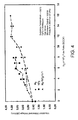
- Fig. 3 is a graph illustrating change in value of the specific dielectric constant k2 by addition of N atoms in the CF film containing N atoms according to the exemplary embodiment of this invention. It is to be noted that the CF film containing N atoms illustrated in Fig. 3 to Fig. 6 is formed by CVD in the apparatus illustrated in Fig.
- the content of N atoms is about 0.7 atom% and the ratio of the number of the F atoms to the number of the C atoms (F/C) is about 1.04, which means the number of the F atoms is larger.
- the N 2 gas can not establish a low dielectric constant at such a flow rate. However, when the flow rate becomes higher and at a flow rate of 14 to 16 sccm, a very low dielectric constant can be accomplished such that k2 becomes about 1.5. In this case, in the CF film containing N atoms, the content of N atoms is about 4.3 atom% and the F/C ratio is about 0.85.
- the mixture of the NF 3 gas and the N 2 gas has a tendency of providing a flow rate-dielectric constant relationship which is intermediate between those of the two gases.
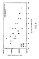
- causing the gas containing N atoms to flow is effective to roughly double the withstand voltage of the CF film containing N atoms from 2.0 MV/cm to 4.0 MV/cm.
- the respective gases it can be seen that, with the NF 3 gas, a high withstand voltage (about 3.50 MV/cm) is obtained at a relatively low flow rate (6 to 8 sccm) and that, with the N 2 gas, a high withstand voltage is not obtained at such a flow rate, but, when the flow rate becomes higher, a higher withstand voltage (about 4.0 MV/cm) is obtained.
- the mixture of the two gases has a tendency of providing a relationship which is intermediate between those of the two gases.
- the withstand voltages of the films (or layers) herein described may be measured by the mercury probe method or the like.
- causing the gas containing N atoms flow serves to reduce the leak current of the CF film containing N atoms.
- the respective gases it can be seen that, with the NF 3 gas, a leak current is reduced at a relatively low flow rate (8 sccm) and that, with the N 2 gas, a small leak current is not obtained at such a flow rate, but, when the flow rate becomes higher, the leak current can be reduced.
- the mixture of the two gases also here, has a tendency of providing a relationship which is intermediate between those of the two gases.
- the leak currents of the films (or layers) herein described may be measured by the mercury probe method or the like.
- Fig. 6 illustrates change in a film remaining rate, namely, a film shrinkage rate when the CF film containing N atoms formed as described above using the NF 3 gas is annealed at 400°C.
- the film shrinkage rates of the films (or layers) herein described may be determined by measuring the film thicknesses before and after the annealing.
- the dielectric constant, the withstand voltage, the amount of the leak current, and the like of the CF film containing N atoms can be appropriately adjusted. More specifically, various characteristics of the CF film can be adjusted by using a desired fluorocarbon compound gas and a desired gas containing N atoms and by appropriately adjusting conditions with reference to the operating conditions according to Fig. 3 to Fig. 6 to form the CF film.
- the specific dielectric constant k2 of the CF film containing N atoms is preferably 1.5 to 2.2. In this case, the withstand voltage and the amount of the leak current of the CF film are also appropriately controlled.
- the CF film contains F atoms and C atoms with the F/C ratio being 0.8 to 1.1, and contains 0.5 to 6 atom% of N atoms.
- the CF film is formed to be relatively thick, and hence a film remaining rate may practically be small to a certain extent.
- the dielectric constant of the CH film is relatively high, and hence the CH film has to be formed as thin as possible. Therefore, it is necessary to make the film remaining rate of the CH film as high as possible, that is, it is necessary to make the shrinkage rate as small as possible.
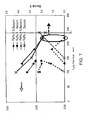
- Fig. 7 is a graph illustrating change in value of the specific dielectric constant k1 and change in film shrinkage rate due to thermal annealing by addition of Si atoms in the CH film containing Si atoms as a barrier layer according to the embodiment of this invention.
- shrinkage means ⁇ (film thickness before annealing) - (film thickness after annealing) ⁇ / (film thickness before annealing).
- the flow rate of the C 4 H 6 gas was 220 sccm and the flow rate of the Si 2 H 6 gas was 4.5 sccm, the obtained shrinkage rate was 0.7% and the obtained value of k1 was 2.88, which are practical values.
- the leak current here was 2.5xE-8 (A/cm 2 ) (in the case of 1 MV/cm), the content of Si atoms in the film was 7 atom%, the content of C atoms was 43 atom%, the content of H atoms was 46.9 atom%, and, in addition, 2.9 atom% of O atoms were contained.
- the dielectric constant, the film shrinkage rate, and the like of the CH film containing Si atoms can be appropriately adjusted. More specifically, by using a desired hydrocarbon compound gas and a desired gas containing Si atoms and appropriately adjusting conditions with reference to the operating conditions according to Fig. 7 to form the CH film, various characteristics of the CH film can be adjusted.
- the specific dielectric constant k1 of the CH film containing Si atoms is preferably 2.8 to 3.0. In this case, the film shrinkage rate is also appropriate.
- the CH film contains H atoms and C atoms with the H/C ratio being 0.8 to 1.2, and contains 2 to 10 atom% of Si atoms.
- the interlayer insulation film, the method of producing the same, the interconnect structure, and the method of producing the same according to this invention are optimum for a semiconductor device or a wiring board including a low-dielectric-constant interlayer insulation film and an interconnect structure, or an electronic device including the semiconductor device and the wiring board.
Landscapes
- Internal Circuitry In Semiconductor Integrated Circuit Devices (AREA)
- Formation Of Insulating Films (AREA)
- Chemical Vapour Deposition (AREA)
Abstract
Description
- This invention relates to a multilayer interconnect structure formed on a substrate or a board, such as a semiconductor element substrate or semiconductor-chip mounting board or a wiring board, and, in particular, to a structure of an interlayer insulation film. This invention also relates to a semiconductor device and a wiring board both of which have the multilayer interconnect structure and to an electronic apparatus including the semiconductor device and the wiring board. Moreover, this invention relates to a method of manufacturing the multilayer interconnect structure and methods of producing or manufacturing the semiconductor device having the multilayer interconnect structure, the wiring board having the multilayer interconnect structure, and the electronic apparatus including the semiconductor device and the wiring board.
- Conventionally, an interlayer insulation film is formed for insulation between interconnect layers included in a multilayer interconnect structure formed on a semiconductor substrate or the like.
- In such a multilayer interconnect structure, a problem of signal delay due to the parasitic capacitance between interconnections and the interconnect resistance has become unignorable, and various kinds of structures have been proposed in order to respond to demands of using an interlayer insulation film of a low dielectric constant (Low-k) (See Patent Document 1).
-
Patent Document 1 proposes the use of a fluorocarbon (CF) film as an interlayer insulation film. The film is formed by using a plasma processing apparatus which uses He, Ne, Ar, Xe, or Kr gas as a gas for generating plasma. In the plasma processing apparatus, use is made of a fluorocarbon gas (hereinafter referred to as a CFx gas, which is, for example, C5F8 gas). In addition, inPatent Document 1, in order to adjust the electron density of the generated plasma, N2, H2, and/or NH3 are/is used in combination with a rare gas for dilution thereof, whereby satisfactory adhesion and a satisfactory shape of the formed film are obtained. - Patent Document 1:
JP-A-2002-220668 - As an exemplary structure of an interlayer insulation film having a low dielectric constant, a proposal is made about obtaining an interlayer insulation film which has a very low dielectric constant and which includes a combination of a fluorocarbon film (hereinafter referred to as a CF film) having a specific dielectric constant k of 2.0 to 2.2 and a hydrocarbon film (hereinafter referred to as a CH film) having a specific dielectric constant k of about 3.0 as a barrier layer of the CF film.
- Such an interlayer insulation film can show satisfactory insulation film characteristics, but, in order to further improve the characteristics of the device, it is still necessary to lower the dielectric constant. However, it has been found out that, if the specific dielectric constants of the respective films are attempted to be further lowered, a problem is caused to occur such that using the CF film brings about a reduction of a withstand voltage and, as a result, about an increase of a leak current. In addition, using the CH film brings about shrinkage of the film (which is shrunk in volume by as much as about 6 %) due to decomposition of a film framework of the CH film during thermal annealing.
- Accordingly, it is an object of this invention to provide an interlayer insulation film which has a low dielectric constant and is stable and in which occurrence of leak current and film shrinkage due to thermal annealing are suppressed.
- It is another object of this invention to provide a method of producing or manufacturing the interlayer insulation film.
- As a result of energetic study to solve the above-mentioned problem, the inventors of this invention found that, by containing N atoms in a CF film, the specific dielectric constant thereof is lowered as compared with that in a conventional case and the withstand voltage is improved to suppress occurrence of leak current, that, by containing Si atoms in a CH film, the specific dielectric constant thereof is lowered as compared with that in a conventional case to suppress film shrinkage due to thermal annealing, and that, by laminating those films, an interlayer insulation film having desired characteristics is obtained, thereby completing this invention.
- Namely, according to this invention, there is provided an interlayer insulation film formed by laminating a hydrocarbon layer containing Si atoms and a fluorocarbon layer containing N atoms, wherein the hydrocarbon layer contains H atoms and C atoms with a ratio of a number of the H atoms to a number of the C atoms (H/C) being from 0.8 to 1.2.
- In addition, according to this invention, there is provided the interlayer insulation film mentioned above, wherein the fluorocarbon layer containing N atoms is laminated on the hydrocarbon layer containing Si atoms.
- Further, according to this invention, there is provided the interlayer insulation film mentioned, wherein a hydrocarbon layer containing Si atoms is further laminated on the fluorocarbon layer containing N atoms.
- Additionally, according to this invention, there is provided any one of the above-mentioned interlayer insulation films, wherein each hydrocarbon layer containing Si atoms has a specific dielectric constant k1 of 2.8 to 3.0.
- According to this invention, there is provided any one of the interlayer insulation films mentioned above, wherein each hydrocarbon layer containing Si atoms contains 2 to 10 atom% of Si atoms.
- According to this invention, there is provided any one of the interlayer insulation films mentioned above, wherein the fluorocarbon layer containing N atoms has a specific dielectric constant k2 of 1.5 to 2.2.
- According to this invention, there is provided any one of the interlayer insulation films mentioned above, wherein the fluorocarbon layer containing N atoms contains F atoms and C atoms with a ratio of a number of the F atoms to a number of the C atoms (F/C) being from 0.8 to 1.1, and contains 0.5 to 6 atom% of N atoms.
- According to this invention, there is provided any one of the interlayer insulation films mentioned above, wherein each hydrocarbon layer containing Si atoms has a thickness of 10 to 50 nm.
- According to this invention, there is provided any one of the interlayer insulation films mentioned above, wherein the fluorocarbon layer containing N atoms has a thickness of 50 to 500 nm.
- According to this invention, there is provided any one of the interlayer insulation films mentioned above, wherein each hydrocarbon layer containing Si atoms is formed by CVD using at least one type of gas containing C atoms and H atoms and a gas containing Si atoms in plasma, the plasma being generated using at least one gas selected from the group consisting of Ar gas, Xe gas, and Kr gas.
- According to this invention, there is provided any one of the interlayer insulation films mentioned above, wherein the fluorocarbon layer containing N atoms is formed by CVD using at least one type of gas containing C atoms and F atoms and a gas containing N atoms in plasma, the plasma being generated using at least one gas selected from the group consisting of Ar gas, Xe gas, and Kr gas.
- According to this invention, there is provided a film forming method of forming an interlayer insulation film, comprising laminating a hydrocarbon layer containing Si atoms and a fluorocarbon layer containing N atoms, wherein the hydrocarbon layer contains H atoms and C atoms with a ratio of a number of the H atoms to a number of the C atoms (H/C) being from 0.8 to 1.2.
- According to this invention, there is provided the film forming method, wherein the fluorocarbon layer containing N atoms is laminated on the hydrocarbon layer containing Si atoms.
- According to this invention, there is provided the film forming method, wherein a hydrocarbon layer containing Si atoms is further laminated on the fluorocarbon layer containing N atoms.
- According to this invention, there is provided any one of the film forming methods mentioned above, wherein each hydrocarbon layer containing Si atoms has a specific dielectric constant k1 of 2.8 to 3.0.
- According to this invention, there is provided any one of the film forming methods mentioned above, wherein each hydrocarbon layer containing Si atoms contains 2 to 10 atom% of Si atoms.
- According to this invention, there is provided any one of the film forming methods mentioned above, wherein the fluorocarbon layer containing N atoms has a specific dielectric constant k2 of 1.5 to 2.2.
- According to this invention, there is provided any one of the film forming methods mentioned above, wherein the fluorocarbon layer containing N atoms contains F atoms and C atoms with a ratio of a number of the F atoms to a number of the C atoms (F/C) being from 0.8 to 1.1, and contains 0.5 to 6 atom% of N atoms.
- According to this invention, there is provided any one of the film forming methods mentioned above, wherein each hydrocarbon layer containing Si atoms has a thickness of 10 to 50 nm.
- According to this invention, there is provided any one of the film forming methods mentioned above, wherein the fluorocarbon layer containing N atoms has a thickness of 50 to 500 nm.
- According to this invention, there is provided any one of the film forming methods mentioned above, wherein each hydrocarbon layer containing Si atoms is formed by CVD using at least one type of gas containing C atoms and H atoms and a gas containing Si atoms in plasma, the plasma being generated using at least one gas selected from the group consisting of Ar gas, Xe gas, and Kr gas.
- According to this invention, there-is provided any one of the film forming methods mentioned above, wherein the fluorocarbon layer containing N atoms is formed by CVD using at least one type of gas containing C atoms and F atoms and a gas containing N atoms in plasma, the plasma being generated using at least one gas selected from the group consisting of Ar gas, Xe gas, and Kr gas.
- According to this invention, there is provided a method of producing a multilayer interconnect structure, comprising: laminating a hydrocarbon layer containing Si atoms and a fluorocarbon layer containing N atoms to form an interlayer insulation film; and embedding a conductor layer in the interlayer insulation film, wherein the hydrocarbon layer contains H atoms and C atoms with a ratio of a number of the H atoms to a number of the C atoms (H/C) being from 0.8 to 1.2.
- According to this invention, there is provided the above-mentioned method of producing a multilayer interconnect structure, wherein the fluorocarbon layer containing N atoms is laminated on the hydrocarbon layer containing Si atoms.
- According to this invention, there is provided the above-mentioned method of producing a multilayer interconnect structure, wherein a hydrocarbon layer containing Si atoms is further laminated on the fluorocarbon layer containing N atoms.
- According to this invention, there is provided any one of the above-mentioned methods of producing a multilayer interconnect structure, wherein each hydrocarbon layer containing Si atoms has a specific dielectric -constant k1 of 2.8 to 3.0.
- According to this invention, there is provided any one of the above-mentioned methods of producing a multilayer interconnect structure, wherein each hydrocarbon layer containing Si atoms contains 2 to 10 atom% of Si atoms.
- According to this invention, there is provided any one of the above-mentioned methods of producing a multilayer interconnect structure, wherein the fluorocarbon layer containing N atoms has a specific dielectric constant k2 of 1.5 to 2.2.
- According to this invention, there is provided any one of the above-mentioned methods of producing a multilayer interconnect structure, wherein the fluorocarbon layer containing N atoms contains F atoms and C atoms with a ratio of a number of the F atoms to a number of the C atoms (F/C) being from 0.8 to 1.1, and contains 0.5 to 6 atom% of N atoms.
- According to this invention, there is provided any one of the above-mentioned methods of producing a multilayer interconnect structure, wherein each hydrocarbon layer containing Si atoms has a thickness of 10 to 50 nm.
- According to this invention, there is provided any one of the above-mentioned methods of producing a multilayer interconnect structure, wherein the fluorocarbon layer containing N atoms has a thickness of 50 to 500 nm.
- According to this invention, there is provided any one of the above-mentioned methods of producing a multilayer interconnect structure, wherein each hydrocarbon layer containing Si atoms is formed by CVD using at least one type of gas containing C atoms and H atoms and a gas containing Si atoms in plasma, the plasma being generated using at least one gas selected from the group consisting of Ar gas, Xe gas, and Kr gas.
- According to this invention, there is provided any one of the above-mentioned methods of producing a multilayer interconnect structure, wherein the fluorocarbon layer containing N atoms is formed by CVD using at least one type of gas containing C atoms and F atoms and a gas containing N atoms in plasma, the plasma being generated using at least one gas selected from the group consisting of Ar gas, Xe gas, and Kr gas.
- According to this invention, there is provided an interconnect structure formed by forming an interlayer insulation film by laminating a hydrocarbon layer containing Si atoms and a fluorocarbon layer containing N atoms and embedding a conductor in the interlayer insulation film, wherein the hydrocarbon layer contains H atoms and C atoms with a ratio of a number of the H atoms to a number of the C atoms (H/C) being from 0.8 to 1.2.
- According to this invention, there is provided the above-mentioned interconnect structure, wherein the fluorocarbon layer containing N atoms is laminated on the hydrocarbon layer containing Si atoms.
- According to this invention, there is provided the above-mentioned interconnect structure, wherein a hydrocarbon layer containing Si atoms is further laminated on the fluorocarbon layer containing N atoms.
- According to this invention, there is provided any one of the above-mentioned interconnect structure, wherein the hydrocarbon layer containing Si atoms has a specific dielectric constant k1 of 2.8 to 3.0.
- According to this invention, there is provided any one of the above-mentioned interconnect structure, wherein each hydrocarbon layer containing Si atoms contains 2 to 10 atom% of Si atoms.
- According to this invention, there is provided any one of the above-mentioned interconnect structure, wherein the fluorocarbon layer containing N atoms has a specific dielectric constant k2 of 1.5 to 2.2.
- According to this invention, there is provided any one of the above-mentioned interconnect structure, wherein the fluorocarbon layer containing N atoms contains F atoms and C atoms with a ratio of a number of the F atoms to a number of the C atoms (F/C) being from 0.8 to 1.1, and contains 0.5 to 6 atom% of N atoms.
- According to this invention, there is provided any one of the above-mentioned interconnect structure, wherein each hydrocarbon layer containing Si atoms has a thickness of 10 to 50 nm.
- According to this invention, there is provided any one of the above-mentioned interconnect structure, wherein the fluorocarbon layer containing N atoms has a thickness of 50 to 500 nm.
- According to this invention, there is provided any one of the above-mentioned interconnect structure, wherein each hydrocarbon layer containing Si atoms is formed by CVD using at least one type of gas containing C atoms and H atoms and a gas containing Si atoms in plasma, the plasma being generated using at least one gas selected from the group consisting of Ar gas, Xe gas, and Kr gas.
- According to this invention, there is provided any one of the above-mentioned interconnect structure, wherein the fluorocarbon layer containing N atoms is formed by CVD using at least one type of gas containing C atoms and F atoms and a gas containing N atoms in plasma, the plasma being generated using at least one gas selected from the group consisting of Ar gas, Xe gas, and Kr gas.
- According to this invention, there is provided a method of producing an interconnect structure, comprising: laminating a hydrocarbon layer containing Si atoms and a fluorocarbon layer containing N atoms to form an interlayer insulation film; and embedding a conductor in the interlayer insulation film, wherein the hydrocarbon layer contains H atoms and C atoms with a ratio of a number of the H atoms to a number of the C atoms (H/C) being from 0.8 to 1.2.
- According to this invention, there is provided the above method of producing an interconnect structure, wherein the fluorocarbon layer containing N atoms is laminated on the hydrocarbon layer containing Si atoms.
- According to this invention, there is provided the above-mentioned method of producing an interconnect structure, wherein a hydrocarbon layer containing Si atoms is further laminated on the fluorocarbon layer containing N atoms.
- According to this invention, there is provided any one of the methods of producing an interconnect structure, wherein each hydrocarbon layer containing Si atoms has a specific dielectric constant k1 of 2.8 to 3.0.
- According to this invention, there is provided any one of the methods of producing an interconnect structure, wherein each hydrocarbon layer containing Si atoms contains 2 to 10 atom% of Si atoms.
- According to this invention, there is provided any one of the methods of producing an interconnect structure, wherein the fluorocarbon layer containing N atoms has a specific dielectric constant k2 of 1.5 to 2.2.
- According to this invention, there is provided any one of the methods of producing an interconnect structure, wherein the fluorocarbon layer containing N atoms contains F atoms and C atoms with a ratio of a number of the F atoms to a number of the C atoms (F/C) being from 0.8 to 1.1, and contains 0.5 to 6 atom% of N atoms.
- According to this invention, there is provided any one of the methods of producing an interconnect structure, wherein each hydrocarbon layer containing Si atoms has a thickness of 10 to 50 nm.
- According to this invention, there is provided any one of the methods of producing an interconnect structure, wherein the fluorocarbon layer containing N atoms has a thickness of 50 to 500 nm.
- According to this invention, there is provided any one of the methods of producing an interconnect structure, wherein the hydrocarbon layer containing Si atoms is formed by CVD using at least one type of gas containing C atoms and H atoms and a gas containing Si atoms in plasma, the plasma being generated using at least one gas selected from the group consisting of Ar gas, Xe gas, and Kr gas.
- According to this invention, there is provided any one of the methods of producing an interconnect structure, wherein the fluorocarbon layer containing N atoms is formed by CVD using at least one type of gas containing C atoms and F atoms and a gas containing N atoms in plasma, the plasma being generated using at least one gas selected from the group consisting of Ar gas, Xe gas, and Kr gas.
- According to this invention, there is provided an electronic device comprising an interlayer insulation film formed by laminating a hydrocarbon layer containing Si atoms and a fluorocarbon layer containing N atoms, wherein the hydrocarbon layer contains H atoms and C atoms with a ratio of a number of the H atoms to a number of the C atoms (H/C) being from 0.8 to 1.2.
- According to this invention, there is provided the above-mentioned electronic device, wherein the fluorocarbon layer containing N atoms is laminated on the hydrocarbon layer containing Si atoms.
- According to this invention, there is provided the above-mentioned electronic device, wherein a hydrocarbon layer containing Si atoms is further laminated on the fluorocarbon layer containing N atoms.
- According to this invention, there is provided any one of the above-mentioned electronic devices, wherein each hydrocarbon layer containing Si atoms has a specific dielectric constant k1 of 2.8 to 3.0.
- According to this invention, there is provided any one of the above-mentioned electronic devices, wherein each hydrocarbon layer containing Si atoms contains 2 to 10 atom% of Si atoms.
- According to this invention, there is provided any one of the above-mentioned electronic devices, wherein the fluorocarbon layer containing N atoms has a specific dielectric constant k2 of 1.5 to 2.2.
- According to this invention, there is provided any one of the above-mentioned electronic devices, wherein the fluorocarbon layer containing N atoms contains F atoms and C atoms with a ratio of a number of the F atoms to a number of the C atoms (F/C) being from 0.8 to 1.1, and contains 0.5 to 6 atom% of N atoms.
- According to this invention, there is provided any one of the above-mentioned electronic devices, wherein each hydrocarbon layer containing Si atoms has a thickness of 10 to 50 nm.
- According to this invention, there is provided any one of the above-mentioned electronic devices, wherein the fluorocarbon layer containing N atoms has a thickness of 50 to 500 nm.
- According to this invention, there is provided any one of the above-mentioned electronic devices, wherein each hydrocarbon layer containing Si atoms is formed by CVD using at least one type of gas containing C atoms and H atoms and a gas containing Si atoms in plasma, the-plasma being generated using at least one gas selected from the group consisting of Ar gas, Xe gas, and Kr gas.
- According to this invention, there is provided any one of the above-mentioned electronic devices, wherein the fluorocarbon layer containing N atoms is formed by CVD using at least one type of gas containing C atoms and F atoms and a gas containing N atoms in plasma, the plasma being generated using at least one gas selected from the group consisting of Ar gas, Xe gas, and Kr gas.
- According to this invention, there is provided a method of producing an electronic device, comprising forming an interlayer insulation film by laminating a hydrocarbon layer containing Si atoms and a fluorocarbon layer containing N atoms, wherein the hydrocarbon layer contains H atoms and C atoms with a ratio of a number of the H atoms to a number of the C atoms (H/C) being from 0.8 to 1.2.
- According to this invention, there is provided the above-mentioned method of producing an electronic device, wherein the fluorocarbon layer containing N atoms is laminated on the hydrocarbon layer containing Si atoms.
- According to this invention, there is provided the above-mentioned method of producing an electronic device, wherein a hydrocarbon layer containing Si atoms is further laminated on the fluorocarbon layer containing N atoms.
- According to this invention, there is provided any one of the methods of producing an electronic device, wherein each hydrocarbon layer containing Si atoms has a specific dielectric constant k1 of 2.8 to 3.0.
- According to this invention, there is provided any one of the methods of producing an electronic device, wherein each hydrocarbon layer containing Si atoms contains 2 to 10 atom% of Si atoms.
- According to this invention, there is provided any one of the methods of producing an electronic device, wherein the fluorocarbon layer containing N atoms has a specific dielectric constant k2 of 1.5 to 2.2.
- According to this invention, there is provided any one of the methods of producing an electronic device, wherein the fluorocarbon layer containing N atoms contains F atoms and C atoms with a ratio of a number of the F atoms to a number of the C atoms (F/C) being from 0.8 to 1.1, and contains 0.5 to 6 atom% of N atoms.
- According to this invention, there is provided any one of the methods of producing an electronic device, wherein each hydrocarbon layer containing Si atoms has a thickness of 10 to 50 nm.
- According to this invention, there is provided any one of the methods of producing an electronic device, wherein the fluorocarbon layer containing N atoms has a thickness of 50 to 500 nm.
- According to this invention, there is provided any one of the methods of producing an electronic device, wherein each hydrocarbon layer containing Si atoms is formed by CVD using at least one type of gas containing C atoms and H atoms and a gas containing Si atoms in plasma, the plasma being generated using at least one gas selected from the group consisting of Ar gas, Xe gas, and Kr gas.
- According to this invention, there is provided any one of the methods of producing an electronic device, wherein the fluorocarbon layer containing N atoms is formed by CVD using at least one type of gas containing C atoms and F atoms and a gas containing N atoms in plasma, the plasma being generated using at least one gas selected from the group consisting of Ar gas, Xe gas, and Kr gas.
- According to this invention, there is provided an interlayer insulation film, which can be used for a semiconductor device and a method of producing the same and which has a low dielectric constant and is stable.
- Further, according to this invention, there is provided an interconnect structure with an interlayer insulation film of a low dielectric constant and a method of manufacturing the same, wherein the interlayer insulation film has an improved withstand voltage and a reduced leak current and, in addition, a reduced amount of shrinkage in volume.
-
-
Fig. 1 is a view illustrating an interconnect structure according to an embodiment of this invention. -
Fig. 2 is a schematic sectional view illustrating a plasma processing apparatus according to the embodiment of this invention. -
Fig. 3 is a graph illustrating change in value of a specific dielectric constant k2 by addition of N atoms in a CF film containing N atoms according to the embodiment of this invention. -
Fig. 4 is a graph illustrating change in an insulation withstand voltage by addition of N atoms in the CF film containing N atoms according to the embodiment of this invention. -
Fig. 5 is a graph illustrating change in leak current density by addition of N atoms in the CF film containing N atoms according to the embodiment of this invention. -
Fig. 6 is a graph illustrating change in film remaining or shrinkage rate by addition of N atoms in the CF film containing N atoms according to the embodiment of this invention. -
Fig. 7 is a graph illustrating change in value of a specific dielectric constant k1 and change in film shrinkage rate due to thermal annealing by addition of Si atoms in a CH film containing Si atoms as a barrier layer according to the embodiment of this invention. -
- 1
- hydrocarbon layer containing Si atoms
- 2
- fluorocarbon layer containing N atoms
- 3
- hydrocarbon layer containing Si atoms
- 4
- via hole
- 5
- groove
- 6
- electrode or wiring
- 7
- wiring conductor (Cu)
- 10
- interconnect structure
- 12
- waveguide
- 13
- gas introduction pipe
- 14
- silicon wafer
- 21
- radial line slot antenna (RLSA)
- 22
- lower shower plate
- 23
- upper shower plate
- 26
- gas introduction pipe
- 31
- process chamber
- An embodiment of this invention is described in the following with reference to the drawings.
-
Fig. 1 is a sectional view illustrating an interconnect structure according to the exemplary embodiment of this invention. As illustrated inFig. 1 , a semiconductor device has a multilayer interconnect structure (only one connecting portion between interconnect layers is illustrated) 10 provided on a semiconductor substrate (not shown) having a number of semiconductor elements formed thereon. The illustratedmultilayer interconnect structure 10 forms an interlayer insulation film and has afirst hydrocarbon layer 1 containing Si atoms which is a hydrocarbon film (hereinafter referred to as a CH film) as a barrier cap layer, afluorocarbon layer 2 containing N atoms as a fluorocarbon film (hereinafter referred to as a CF film) laminated on thefirst hydrocarbon layer 1, and further, asecond hydrocarbon layer 3 containing Si atoms, which is a CH film as a barrier layer and which is laminated on thefluorocarbon layer 2. - Here, the first and
second hydrocarbon layers fluorocarbon layer 2 contain F atoms and C atoms at the ratio of the number of the F atoms to the number of the C atoms (F/C) which falls within a range between 0.8 and 1.1. - The ratios of the respective atoms in the films (or layers) herein described may be determined by X-ray photoelectron spectroscopy (XPS) or Rutherford Backscattering Spectrometry /Hydrogen Forward Spectrometry (RBS/HFS).
- A via
hole 4 is provided which is passed through thefirst hydrocarbon layer 1 and a lower part of thefluorocarbon layer 2. On an inner wall of the viahole 4, a film made of a fluoride of nickel, preferably, nickel (II) fluoride (namely, nickel difluoride) (expressed as NiF2), is formed as adiffusion preventing layer 8 forCu wiring 6 by forming a nickel film by PVD and then fluorinating the film, or by directly forming the film made of the fluoride of nickel by MOCVD. - An electrode or
wiring 6 of Cu is formed in the viahole 4. Agroove 5 is formed so as to allow the remaining part (upper part) of thefluorocarbon layer 2 and thehydrocarbon layer 3 to pass therethrough. A film of a fluoride made of nickel, preferably nickel (II) fluoride (expressed as NiF2), is similarly formed on an inner wall of the groove as adiffusion preventing layer 9 forCu wiring 7. Awiring conductor 7 made of Cu is embedded in thegroove 5. - From the viewpoint of drastically lowering the dielectric constant of the interlayer insulation film as a whole compared with that of a conventional interlayer insulation film, each specific dielectric constant k1 of the hydrocarbon layers containing Si atoms which form the
first hydrocarbon layer 1 and thesecond hydrocarbon layer 3 is preferably 2.8 to 3.0. From a similar viewpoint, a specific dielectric constant k2 of the fluorocarbon layer containing N atoms which forms thefluorocarbon layer 2 is preferably 1.5 to 2.2. - The specific dielectric constants of the films (or layers) herein described may be measured by a mercury probe method or the like.
- The thicknesses of the hydrocarbon layers containing Si atoms which form the first and
second hydrocarbon layers fluorocarbon layer 2 is, though not particularly limited, usually 50 to 500 nm. - In
Fig. 1 , the illustrated interlayer insulation film is formed by laminating the CH films and the CF film, i.e., thefirst hydrocarbon layer 1 containing Si atoms, thefluorocarbon layer 2 containing N atoms, and thesecond hydrocarbon layer 3 containing Si atoms in the stated order. However, the order of lamination of the CH film(s) and the CF film(s) and the number of the laminated CH film(s) and the CF film(s) according to this invention are not specifically limited as long as the desired effect of this invention is not prevented and another film made of an arbitrary material may be inserted between a CH film and a CF film therein. -
Fig. 2 is a schematic sectional view illustrating a plasma processing apparatus according to the exemplary embodiment of this invention. Referring toFig. 2 , amicrowave 17 is supplied through awaveguide 12 to a radial line slot antenna (RLSA) 21 disposed above a containermain body 20 of theplasma processing apparatus 102 via aninsulator plate 15. Thereafter, themicrowave 17 is transmitted from the radial line slot antenna (RLSA) 21 through theinsulator plate 15 to anupper shower plate 23 located under theRLSA 21 and is emitted into aplasma generating region 16. As a plasma excitation gas for exciting plasma, usually, at least one rare gas selected from the group consisting of Ar gas, Xe gas, and Kr gas is uniformly ejected into theplasma generating region 16 from theupper shower plate 23 via agas introduction pipe 13, and plasma is excited by the microwave emitted thereinto. - A
lower shower plate 22 is disposed in a diffusion plasma region of theplasma processing apparatus 102. - Here, when the rare gas is caused to flow into the
upper shower plate 23 via thegas introduction pipe 13 and SiH4 gas is caused to flow into thelower shower plate 22 via agas introduction pipe 26, a silicon (Si) film is formed on the surface of a substrate, for example, asilicon wafer 14. - In addition, if the rare gas is passed from the
upper shower plate 23, and a gas of a compound containing a C atom and an F atom, in general, a fluorocarbon compound gas is passed from thelower shower plate 22, a CF membrane or film is formed. In this invention, a fluorocarbon compound gas and a gas containing an N atom (in general, at least one selected from the group consisting of N2 gas, NF3 gas, and NH3 gas) are simultaneously passed from thelower shower plate 22 and, as a result, an N atom-containing fluorocarbon layer is formed. The fluorocarbon compound gas is not particularly limited, and from the viewpoint of polymerization, a gas formed of a compound represented by the formula: CpFq (where p and q satisfy the formulae: p≥4 and 1.5≤p/q≤2.0) is preferred and a gas formed of at least one compound selected from the group consisting of C4F6, C4F8, and C5F8) is more preferred. Hexafluorocyclobutadiene, hexafluoro-2-butyne, and the like are given as C4F6, octafluorocyclobutane, octafluoro-2-butene, and the like are given as C4F8, and octafluorocyclopentene, octafluoro-2-pentyne, octafluoro-1,4-pentadiene, octafluoro-1,3-pentadiene, octafluoro(isoprene), and the like are given as C5F8. - On the other hand, the rare gas is passed from the
upper shower plate 23, and a gas of a compound containing a C atom and an H atom, in general, a hydrocarbon compound gas and a gas containing an Si atom (in general, Si2H6 gas) are passed from thelower shower plate 22, and an Si atom-containing hydrocarbon layer is formed. The hydrocarbon compound gas is not particularly limited, and from the viewpoint of polymerization, a gas formed of a unsaturated hydrocarbon represented by the formula: CmH2m-2 (where m represents 4 to 6) is preferred and a gas formed of at least one compound selected from the group consisting of C4H6, C5H8, and C6H10 is more preferred. Butadiene, 2-butyne, cyclobutene, and the like are given as C4H6, 1,3-pentadiene, 1,4-pentadiene, isoprene, cyclopentene, 1-pentyne, 2-pentyne, and the like are given as C5H8, and 3-methyl-1-pentyne, 3,3-dimethyl-1-butyne, cyclohexene, and the like are given as C6H10. - Exhaust gases in a
process chamber 31 pass through an exhaust duct via exhaust ports (not shown) and then are each introduced into a small pump from any one of inlet ports of the small pump. - Next, description is made about a method of manufacturing the interconnect structure illustrated in
Fig. 1 according to the embodiment of this invention. In order to manufacture the illustrated structure, thehydrocarbon layer 1 containing Si atoms is at first formed as a barrier cap layer and, thereafter, thefluorocarbon layer 2 containing N atoms, and thehydrocarbon layer 3 containing Si atoms as another barrier layer are formed successively in the stated order. The successive film formation can be carried out in theplasma processing apparatus 102 illustrated inFig. 2 , with the rare gas flowing from theupper shower plate 23 and with a hydrocarbon compound gas and a gas containing Si atoms flowing from thelower shower plate 22. Thus, thehydrocarbon layer 1 containing Si atoms is formed by CVD. Then, the gas which flows through thelower shower plate 22 is switched to a mixture of a fluorocarbon compound gas and a gas containing N atoms to form thefluorocarbon layer 2 containing N atoms by CVD. Thereafter, the gas which flows through thelower shower plate 22 is switched to a hydrocarbon compound gas and a gas containing Si atoms to form thehydrocarbon layer 3 containing Si atoms by CVD. - Then, the via
hole 4 which passes through thehydrocarbon layer 1 containing Si atoms and the lower part of thefluorocarbon layer 2 containing N atoms is formed and, thereafter, thegroove 5 which passes through the remaining part (upper part) of thefluorocarbon layer 2 containing N atoms and thehydrocarbon layer 3 containing Si atoms is formed. As a barrier layer for preventing diffusion of the electrode metal into the interlayer insulation film, thefilms hole 4 and thegroove 5, respectively, by forming nickel films by PVD and then fluorinating the films, or by directly forming the films made of the fluoride of nickel by MOCVD. The viahole 4 and thegroove 5 may be formed by first forming thegroove 5 and then masking the inner wall of thegroove 5 at a predetermined thickness to form the viahole 4. Alternatively, thegroove 5 may be formed by forming a hole having the same inner diameter as that of the viahole 4 and then widening the upper part into the viahole 4 with an inner surface of the part of the viahole 4 being masked. After that, the viahole 4 and thegroove 5 are filled with Cu to form theconductors interlayer interconnect structure 10 is completed. - Next, description is made more in detail about physical properties of a CF film containing N atoms (corresponding to the fluorocarbon layer containing N atoms) and a CH film containing Si atoms (corresponding to the hydrocarbon layers containing Si atoms) according to the exemplary embodiment of this invention.
-
Fig. 3 is a graph illustrating change in value of the specific dielectric constant k2 by addition of N atoms in the CF film containing N atoms according to the exemplary embodiment of this invention. It is to be noted that the CF film containing N atoms illustrated inFig. 3 to Fig. 6 is formed by CVD in the apparatus illustrated inFig. 2 at a pressure of 280 millitorr (mTorr) (= 37.2 Pa) and at a microwave output of 1,500 W with the substrate temperature kept at 350°C, the flow rate of Ar being 480 sccm, and the flow rate of C5F8 (octafluorocyclopentene) being 50 sccm, by using N2 gas, NF3 gas, or a mixture of both of the N2 gas and the NF3 gas [N2/NF3 = 1/1 (volume ratio)] as a gas containing N atoms and changing the flow rates of the gases containing N atoms. - As illustrated in
Fig. 3 , it can be seen that, by causing the gas containing N atoms to flow, the value of k2 of the CF film containing N atoms is lowered from 2.2 to about 1.5. With regard to the respective gases, the NF3 gas makes it possible to obtain a low dielectric constant (k = about 1.6) at a relatively low flow rate (6 to 8 sccm). In this case, in the CF film containing N atoms, the content of N atoms is about 0.7 atom% and the ratio of the number of the F atoms to the number of the C atoms (F/C) is about 1.04, which means the number of the F atoms is larger. The N2 gas can not establish a low dielectric constant at such a flow rate. However, when the flow rate becomes higher and at a flow rate of 14 to 16 sccm, a very low dielectric constant can be accomplished such that k2 becomes about 1.5. In this case, in the CF film containing N atoms, the content of N atoms is about 4.3 atom% and the F/C ratio is about 0.85. The mixture of the NF3 gas and the N2 gas has a tendency of providing a flow rate-dielectric constant relationship which is intermediate between those of the two gases. - With reference to
Fig. 4 , it can be seen that causing the gas containing N atoms to flow is effective to roughly double the withstand voltage of the CF film containing N atoms from 2.0 MV/cm to 4.0 MV/cm. With regard to the respective gases, it can be seen that, with the NF3 gas, a high withstand voltage (about 3.50 MV/cm) is obtained at a relatively low flow rate (6 to 8 sccm) and that, with the N2 gas, a high withstand voltage is not obtained at such a flow rate, but, when the flow rate becomes higher, a higher withstand voltage (about 4.0 MV/cm) is obtained. The mixture of the two gases has a tendency of providing a relationship which is intermediate between those of the two gases. - The withstand voltages of the films (or layers) herein described may be measured by the mercury probe method or the like.
- With reference to
Fig. 5 , it can be seen that causing the gas containing N atoms flow serves to reduce the leak current of the CF film containing N atoms. With regard to the respective gases, it can be seen that, with the NF3 gas, a leak current is reduced at a relatively low flow rate (8 sccm) and that, with the N2 gas, a small leak current is not obtained at such a flow rate, but, when the flow rate becomes higher, the leak current can be reduced. The mixture of the two gases, also here, has a tendency of providing a relationship which is intermediate between those of the two gases. - The leak currents of the films (or layers) herein described may be measured by the mercury probe method or the like.
-
Fig. 6 illustrates change in a film remaining rate, namely, a film shrinkage rate when the CF film containing N atoms formed as described above using the NF3 gas is annealed at 400°C. When the film is formed with the pressure in the chamber being 400 mTorr (= 53.2 Pa) and the flow rate of NF3 being 6 sccm, the value of k2 is 1.58 and the film remaining rate is 86%. - The film shrinkage rates of the films (or layers) herein described may be determined by measuring the film thicknesses before and after the annealing.
- From the above, it can be seen that, when a consumed amount of the gas containing N atoms is adjusted in relation to the fluorocarbon compound gas, the dielectric constant, the withstand voltage, the amount of the leak current, and the like of the CF film containing N atoms can be appropriately adjusted. More specifically, various characteristics of the CF film can be adjusted by using a desired fluorocarbon compound gas and a desired gas containing N atoms and by appropriately adjusting conditions with reference to the operating conditions according to
Fig. 3 to Fig. 6 to form the CF film. The specific dielectric constant k2 of the CF film containing N atoms is preferably 1.5 to 2.2. In this case, the withstand voltage and the amount of the leak current of the CF film are also appropriately controlled. The CF film contains F atoms and C atoms with the F/C ratio being 0.8 to 1.1, and contains 0.5 to 6 atom% of N atoms. - In the interlayer insulation film formed by laminating the CF film(s) and the CH film(s), the CF film is formed to be relatively thick, and hence a film remaining rate may practically be small to a certain extent. On the other hand, the dielectric constant of the CH film is relatively high, and hence the CH film has to be formed as thin as possible. Therefore, it is necessary to make the film remaining rate of the CH film as high as possible, that is, it is necessary to make the shrinkage rate as small as possible. Next, physical properties of a CH film containing Si atoms according to this invention are described.
-
Fig. 7 is a graph illustrating change in value of the specific dielectric constant k1 and change in film shrinkage rate due to thermal annealing by addition of Si atoms in the CH film containing Si atoms as a barrier layer according to the embodiment of this invention. The CH film containing Si atoms illustrated inFig. 7 is formed by CVD in the apparatus illustrated inFig. 2 at a pressure of 40 mTorr (= 37.2 Pa) and at a microwave output of 3,000 W with the substrate temperature being 380°C, the flow rate of Ar being 200 sccm, and the flow rates of C4H6 (2-butine) gas and Si2H6 gas being varied to be 80 to 240 sccm and 2 to 5 sccm, respectively. - As illustrated in
Fig. 7 , as the flow rate of the C4H6 gas becomes higher, the value of k1 is more improved. On the other hand, there is a tendency that the extent of the shrinkage is more improved as the amount of the Si2H6 gas is larger. It is to be noted that the term "shrinkage" as used herein means {(film thickness before annealing) - (film thickness after annealing)} / (film thickness before annealing). Actually, when the flow rate of the C4H6 gas was 220 sccm and the flow rate of the Si2H6 gas was 4.5 sccm, the obtained shrinkage rate was 0.7% and the obtained value of k1 was 2.88, which are practical values. The leak current here was 2.5xE-8 (A/cm2) (in the case of 1 MV/cm), the content of Si atoms in the film was 7 atom%, the content of C atoms was 43 atom%, the content of H atoms was 46.9 atom%, and, in addition, 2.9 atom% of O atoms were contained. The density of the film was 1.26 g/cm3 (= 1,260 kg/m3). - From the above, it can be seen that, by adjusting the amount of usage of the gas containing Si atoms in relation to the hydrocarbon compound gas, the dielectric constant, the film shrinkage rate, and the like of the CH film containing Si atoms can be appropriately adjusted. More specifically, by using a desired hydrocarbon compound gas and a desired gas containing Si atoms and appropriately adjusting conditions with reference to the operating conditions according to
Fig. 7 to form the CH film, various characteristics of the CH film can be adjusted. The specific dielectric constant k1 of the CH film containing Si atoms is preferably 2.8 to 3.0. In this case, the film shrinkage rate is also appropriate. The CH film contains H atoms and C atoms with the H/C ratio being 0.8 to 1.2, and contains 2 to 10 atom% of Si atoms. - As described above, the interlayer insulation film, the method of producing the same, the interconnect structure, and the method of producing the same according to this invention are optimum for a semiconductor device or a wiring board including a low-dielectric-constant interlayer insulation film and an interconnect structure, or an electronic device including the semiconductor device and the wiring board.
Claims (77)
- An interlayer insulation film formed by laminating a hydrocarbon layer containing Si atoms and a fluorocarbon layer containing N atoms, wherein the hydrocarbon layer contains H atoms and C atoms with a ratio of a number of the H atoms to a number of the C atoms (H/C) being from 0.8 to 1.2.
- An interlayer insulation film according to claim 1, wherein the fluorocarbon layer containing N atoms is laminated on the hydrocarbon layer containing Si atoms.
- An interlayer insulation film according to claim 2, wherein a hydrocarbon layer containing Si atoms is further laminated on the fluorocarbon layer containing N atoms.
- An interlayer insulation film according to any one of claims 1 to 3, wherein each hydrocarbon layer containing Si atoms has a specific dielectric constant k1 of 2.8 to 3.0.
- An interlayer insulation film according to any one of claims 1 to 4, wherein each hydrocarbon layer containing Si atoms contains 2 to 10 atom% of Si atoms.
- An interlayer insulation film according to any one of claims 1 to 5, wherein the fluorocarbon layer containing N atoms has a specific dielectric constant k2 of 1.5 to 2.2.
- An interlayer insulation film according to any one of claims 1 to 6, wherein the fluorocarbon layer containing N atoms contains F atoms and C atoms with a ratio of a number of the F atoms to a number of the C atoms (F/C) being from 0.8 to 1.1, and contains 0.5 to 6 atom% of N atoms.
- An interlayer insulation film according to any one of claims 1 to 7, wherein each hydrocarbon layer containing Si atoms has a thickness of 10 to 50 nm.
- An interlayer insulation film according to any one of claims 1 to 8, wherein the fluorocarbon layer containing N atoms has a thickness of 50 to 500 nm.
- An interlayer insulation film according to any one of claims 1 to 9, wherein each hydrocarbon layer containing Si atoms is formed by CVD using at least one type of gas containing C atoms and H atoms and a gas containing Si atoms in plasma, the plasma being generated using at least one gas selected from the group consisting of Ar gas, Xe gas, and Kr gas.
- An interlayer insulation film according to any one of claims 1 to 10, wherein the fluorocarbon layer containing N atoms is formed by CVD using at least one type of gas containing C atoms and F atoms and a gas containing N atoms in plasma, the plasma being generated using at least one gas selected from the group consisting of Ar gas, Xe gas, and Kr gas.
- A film forming method of forming an interlayer insulation film, comprising laminating a hydrocarbon layer containing Si atoms and a fluorocarbon layer containing N atoms, wherein the hydrocarbon layer contains H atoms and C atoms with a ratio of a number of the H atoms to a number of the C atoms (H/C) being from 0.8 to 1.2.
- A film forming method according to claim 12, wherein the fluorocarbon layer containing N atoms is laminated on the hydrocarbon layer containing Si atoms.
- A film forming method according to claim 13, wherein a hydrocarbon layer containing Si atoms is further laminated on the fluorocarbon layer containing N atoms.
- A film forming method according to any one of claims 12 to 14, wherein each hydrocarbon layer containing Si atoms has a specific dielectric constant k1 of 2.8 to 3.0.
- A film forming method according to any one of claims 12 to 15, wherein each hydrocarbon layer containing Si atoms contains 2 to 10 atom% of Si atoms.
- A film forming method according to any one of claims 12 to 16, wherein the fluorocarbon layer containing N atoms has a specific dielectric constant k2 of 1.5 to 2.2.
- A film forming method according to any one of claims 12 to 17, wherein the fluorocarbon layer containing N atoms contains F atoms and C atoms with a ratio of a number of the F atoms to a number of the C atoms (F/C) being from 0.8 to 1.1, and contains 0.5 to 6 atom% of N atoms.
- A film forming method according to any one of claims 12 to 18, wherein each hydrocarbon layer containing Si atoms has a thickness of 10 to 50 nm.
- A film forming method according to any one of claims 12 to 19, wherein the fluorocarbon layer containing N atoms has a thickness of 50 to 500 nm.
- A film forming method according to any one of claims 12 to 20, wherein each hydrocarbon layer containing Si atoms is formed by CVD using at least one type of gas containing C atoms and H atoms and a gas containing Si atoms in plasma, the plasma being generated using at least one gas selected from the group consisting of Ar gas, Xe gas, and Kr gas.
- A film forming method according to any one of claims 12 to 21, wherein the fluorocarbon layer containing N atoms is formed by CVD using at least one type of gas containing C atoms and F atoms and a gas containing N atoms in plasma, the plasma being generated using at least one gas selected from the group consisting of Ar gas, Xe gas, and Kr gas.
- A method of producing a multilayer interconnect structure, comprising:laminating a hydrocarbon layer containing Si atoms and a fluorocarbon layer containing N atoms to form an interlayer insulation film; andembedding a conductor layer in the interlayer insulation film,wherein the hydrocarbon layer contains H atoms and C atoms with a ratio of a number of the H atoms to a number of the C atoms (H/C) being from 0.8 to 1.2.
- A method of producing a multilayer interconnect structure according to claim 23, wherein the fluorocarbon layer containing N atoms is laminated on the hydrocarbon layer containing Si atoms.
- A method of producing a multilayer interconnect structure according to claim 24, wherein a hydrocarbon layer containing Si atoms is further laminated on the fluorocarbon layer containing N atoms.
- A method of producing a multilayer interconnect structure according to any one of claims 23 to 25, wherein each hydrocarbon layer containing Si atoms has a specific dielectric constant k1 of 2.8 to 3.0.
- A method of producing a multilayer interconnect structure according to any one of claims 23 to 26, wherein each hydrocarbon layer containing Si atoms contains 2 to 10 atom% of Si atoms.
- A method of producing a multilayer interconnect structure according to any one of claims 23 to 27, wherein the fluorocarbon layer containing N atoms has a specific dielectric constant k2 of 1.5 to 2.2.
- A method of producing a multilayer interconnect structure according to any one of claims 23 to 28, wherein the fluorocarbon layer containing N atoms contains F atoms and C atoms with a ratio of a number of the F atoms to a number of the C atoms (F/C) being from 0.8 to 1.1, and contains 0.5 to 6 atom% of N atoms.
- A method of producing a multilayer interconnect structure according to any one of claims 23 to 29, wherein each hydrocarbon layer containing Si atoms has a thickness of 10 to 50 nm.
- A method of producing a multilayer interconnect structure according to any one of claims 23 to 30, wherein the fluorocarbon layer containing N atoms has a thickness of 50 to 500 nm.
- A method of producing a multilayer interconnect structure according to any one of claims 23 to 31, wherein each hydrocarbon layer containing Si atoms is formed by CVD using at least one type of gas containing C atoms and H atoms and a gas containing Si atoms in plasma, the plasma being generated using at least one gas selected from the group consisting of Ar gas, Xe gas, and Kr gas.
- A method of producing a multilayer interconnect structure according to any one of claims 23 to 32, wherein the fluorocarbon layer containing N atoms is formed by CVD using at least one type of gas containing C atoms and F atoms and a gas containing N atoms in plasma, the plasma being generated using at least one gas selected from the group consisting of Ar gas, Xe gas, and Kr gas.
- An interconnect structure formed by forming an interlayer insulation film by laminating a hydrocarbon layer containing Si atoms and a fluorocarbon layer containing N atoms and embedding a conductor in the interlayer insulation film, wherein the hydrocarbon layer contains H atoms and C atoms with a ratio of a number of the H atoms to a number of the C atoms (H/C) being from 0.8 to 1.2.
- An interconnect structure according to claim 34, wherein the fluorocarbon layer containing N atoms is laminated on the hydrocarbon layer containing Si atoms.
- An interconnect structure according to claim 35, wherein a hydrocarbon layer containing Si atoms is further laminated on the fluorocarbon layer containing N atoms.
- An interconnect structure according to any one of claims 34 to 36, wherein the hydrocarbon layer containing Si atoms has a specific dielectric constant k1 of 2.8 to 3.0.
- An interconnect structure according to any one of claims 34 to 37, wherein each hydrocarbon layer containing Si atoms contains 2 to 10 atom% of Si atoms.
- An interconnect structure according to any one of claims 34 to 38, wherein the fluorocarbon layer containing N atoms has a specific dielectric constant k2 of 1.5 to 2.2.
- An interconnect structure according to any one of claims 34 to 39, wherein the fluorocarbon layer containing N atoms contains F atoms and C atoms with a ratio of a number of the F atoms to a number of the C atoms (F/C) being from 0.8 to 1.1, and contains 0.5 to 6 atom% of N atoms.
- An interconnect structure according to any one of claims 34 to 40, wherein each hydrocarbon layer containing Si atoms has a thickness of 10 to 50 nm.
- An interconnect structure according to any one of claims 34 to 41, wherein the fluorocarbon layer containing N atoms has a thickness of 50 to 500 nm.
- An interconnect structure according to any one of claims 34 to 42, wherein each hydrocarbon layer containing Si atoms is formed by CVD using at least one type of gas containing C atoms and H atoms and a gas containing Si atoms in plasma, the plasma being generated using at least one gas selected from the group consisting of Ar gas, Xe gas, and Kr gas.
- An interconnect structure according to any one of claims 34 to 43, wherein the fluorocarbon layer containing N atoms is formed by CVD using at least one type of gas containing C atoms and F atoms and a gas containing N atoms in plasma, the plasma being generated using at least one gas selected from the group consisting of Ar gas, Xe gas, and Kr gas.
- A method of producing an interconnect structure, comprising:laminating a hydrocarbon layer containing Si atoms and a fluorocarbon layer containing N atoms to form an interlayer insulation film; andembedding a conductor in the interlayer insulation film,wherein the hydrocarbon layer contains H atoms and C atoms with a ratio of a number of the H atoms to a number of the C atoms (H/C) being from 0.8 to 1.2.
- A method of producing an interconnect structure according to claim 45, wherein the fluorocarbon layer containing N atoms is laminated on the hydrocarbon layer containing Si atoms.
- A method of producing an interconnect structure according to claim 46, wherein a hydrocarbon layer containing Si atoms is further laminated on the fluorocarbon layer containing N atoms.
- A method of producing an interconnect structure according to any one of claims 45 to 47, wherein each hydrocarbon layer containing Si atoms has a specific dielectric constant k1 of 2.8 to 3.0.
- A method of producing an interconnect structure according to any one of claims 45 to 48, wherein each hydrocarbon layer containing Si atoms contains 2 to 10 atom% of Si atoms.
- A method of producing an interconnect structure according to any one of claims 45 to 49, wherein the fluorocarbon layer containing N atoms has a specific dielectric constant k2 of 1.5 to 2.2.
- A method of producing an interconnect structure according to any one of claims 45 to 50, wherein the fluorocarbon layer containing N atoms contains F atoms and C atoms with a ratio of a number of the F atoms to a number of the C atoms (F/C) being from 0.8 to 1.1, and contains 0.5 to 6 atom% of N atoms.
- A method of producing an interconnect structure according to any one of claims 45 to 51, wherein each hydrocarbon layer containing Si atoms has a thickness of 10 to 50 nm.
- A method of producing an interconnect structure according to any one of claims 45 to 52, wherein the fluorocarbon layer containing N atoms has a thickness of 50 to 500 nm.
- A method of producing an interconnect structure according to any one of claims 45 to 53, wherein the hydrocarbon layer containing Si atoms is formed by CVD using at least one type of gas containing C atoms and H atoms and a gas containing Si atoms in plasma, the plasma being generated using at least one gas selected from the group consisting of Ar gas, Xe gas, and Kr gas.
- A method of producing an interconnect structure according to any one of claims 45 to 54, wherein the fluorocarbon layer containing N atoms is formed by CVD using at least one type of gas containing C atoms and F atoms and a gas containing N atoms in plasma, the plasma being generated using at least one gas selected from the group consisting of Ar gas, Xe gas, and Kr gas.
- An electronic device comprising an interlayer insulation film formed by laminating a hydrocarbon layer containing Si atoms and a fluorocarbon layer containing N atoms, wherein the hydrocarbon layer contains H atoms and C atoms with a ratio of a number of the H atoms to a number of the C atoms (H/C) being from 0.8 to 1.2.
- An electronic device according to claim 56, wherein the fluorocarbon layer containing N atoms is laminated on the hydrocarbon layer containing Si atoms.
- An electronic device according to claim 57, wherein a hydrocarbon layer containing Si atoms is further laminated on the fluorocarbon layer containing N atoms.
- An electronic device according to any one of claims 56 to 58, wherein each hydrocarbon layer containing Si atoms has a specific dielectric constant k1 of 2.8 to 3.0.
- An electronic device according to any one of claims 56 to 59, wherein each hydrocarbon layer containing Si atoms contains 2 to 10 atom% of Si atoms.
- An electronic device according to any one of claims 56 to 60, wherein the fluorocarbon layer containing N atoms has a specific dielectric constant k2 of 1.5 to 2.2.
- An electronic device according to any one of claims 56 to 61, wherein the fluorocarbon layer containing N atoms contains F atoms and C atoms with a ratio of a number of the F atoms to a number of the C atoms (F/C) being from 0.8 to 1.1, and contains 0.5 to 6 atom% of N atoms.
- An electronic device according to any one of claims 56 to 62, wherein each hydrocarbon layer containing Si atoms has a thickness of 10 to 50 nm.
- An electronic device according to any one of claims 56 to 63, wherein the fluorocarbon layer containing N atoms has a thickness of 50 to 500 nm.
- An electronic device according to any one of claims 56 to 64, wherein each hydrocarbon layer containing Si atoms is formed by CVD using at least one type of gas containing C atoms and H atoms and a gas containing Si atoms in plasma, the plasma being generated using at least one gas selected from the group consisting of Ar gas, Xe gas, and Kr gas.
- An electronic device according to any one of claims 56 to 65, wherein the fluorocarbon layer containing N atoms is formed by CVD using at least one type of gas containing C atoms and F atoms and a gas containing N atoms in plasma, the plasma being generated using at least one gas selected from the group consisting of Ar gas, Xe gas, and Kr gas.
- A method of producing an electronic device, comprising forming an interlayer insulation film by laminating a hydrocarbon layer containing Si atoms and a fluorocarbon layer containing N atoms, wherein the hydrocarbon layer contains H atoms and C atoms with a ratio of a number of the H atoms to a number of the C atoms (H/C) being from 0.8 to 1.2.
- A method of producing an electronic device according to claim 67, wherein the fluorocarbon layer containing N atoms is laminated on the hydrocarbon layer containing Si atoms.
- A method of producing an electronic device according to claim 68, wherein a hydrocarbon layer containing Si atoms is further laminated on the fluorocarbon layer containing N atoms.
- A method of producing an electronic device according to any one of claims 67 to 69, wherein each hydrocarbon layer containing Si atoms has a specific dielectric constant k1 of 2.8 to 3.0.
- A method of producing an electronic device according to any one of claims 67 to 70, wherein each hydrocarbon layer containing Si atoms contains 2 to 10 atom% of Si atoms.
- A method of producing an electronic device according to any one of claims 67 to 71, wherein the fluorocarbon layer containing N atoms has a specific dielectric constant k2 of 1.5 to 2.2.
- A method of producing an electronic device according to any one of claims 67 to 72, wherein the fluorocarbon layer containing N atoms contains F atoms and C atoms with a ratio of a number of the F atoms to a number of the C atoms (F/C) being from 0.8 to 1.1, and contains 0.5 to 6 atom% of N atoms.
- A method of producing an electronic device according to any one of claims 67 to 73, wherein each hydrocarbon layer containing Si atoms has a thickness of 10 to 50 nm.
- A method of producing an electronic device according to any one of claims 67 to 74, wherein the fluorocarbon layer containing N atoms has a thickness of 50 to 500 nm.
- A method of producing an electronic device according to any one of claims 67 to 75, wherein each hydrocarbon layer containing Si atoms is formed by CVD using at least one type of gas containing C atoms and H atoms and a gas containing Si atoms in plasma, the plasma being generated using at least one gas selected from the group consisting of Ar gas, Xe gas, and Kr gas.
- A method of producing an electronic device according to any one of claims 67 to 76, wherein the fluorocarbon layer containing N atoms is formed by CVD using at least one type of gas containing C atoms and F atoms and a gas containing N atoms in plasma, the plasma being generated using at least one gas selected from the group consisting of Ar gas, Xe gas, and Kr gas.
Applications Claiming Priority (2)
| Application Number | Priority Date | Filing Date | Title |
|---|---|---|---|
| JP2007050236A JP5074059B2 (en) | 2007-02-28 | 2007-02-28 | Interlayer insulating film and wiring structure, and manufacturing method thereof |
| PCT/JP2008/053083 WO2008105344A1 (en) | 2007-02-28 | 2008-02-22 | Interlayer insulation film, interconnect structure, and methods for production thereof |
Publications (3)
| Publication Number | Publication Date |
|---|---|
| EP2117037A1 true EP2117037A1 (en) | 2009-11-11 |
| EP2117037A4 EP2117037A4 (en) | 2010-10-20 |
| EP2117037B1 EP2117037B1 (en) | 2012-12-19 |
Family
ID=39721179
Family Applications (1)
| Application Number | Title | Priority Date | Filing Date |
|---|---|---|---|
| EP08711851A Not-in-force EP2117037B1 (en) | 2007-02-28 | 2008-02-22 | Interlayer insulation film, and methods for production thereof |
Country Status (7)
| Country | Link |
|---|---|
| US (1) | US20100101834A1 (en) |
| EP (1) | EP2117037B1 (en) |
| JP (1) | JP5074059B2 (en) |
| KR (1) | KR101107569B1 (en) |
| CN (1) | CN101622699B (en) |
| TW (1) | TW200901320A (en) |
| WO (1) | WO2008105344A1 (en) |
Families Citing this family (4)
| Publication number | Priority date | Publication date | Assignee | Title |
|---|---|---|---|---|
| WO2011055644A1 (en) | 2009-11-06 | 2011-05-12 | Semiconductor Energy Laboratory Co., Ltd. | Method for manufacturing semiconductor device |
| JP2011181672A (en) * | 2010-03-01 | 2011-09-15 | Taiyo Nippon Sanso Corp | Low-permittivity interlayer insulation film, and method of forming the same |
| WO2013099300A1 (en) * | 2011-12-28 | 2013-07-04 | 国立大学法人東北大学 | Wiring structure, semiconductor device provided with wiring structure, and method for manufacturing said semiconductor device |
| TWI627192B (en) * | 2015-03-13 | 2018-06-21 | Murata Manufacturing Co., Ltd. | Atomic layer deposition inhibiting material |
Family Cites Families (9)
| Publication number | Priority date | Publication date | Assignee | Title |
|---|---|---|---|---|
| CA2157257C (en) * | 1994-09-12 | 1999-08-10 | Kazuhiko Endo | Semiconductor device with amorphous carbon layer and method of fabricating the same |
| SG53005A1 (en) * | 1996-07-03 | 1998-09-28 | Novellus Systems Inc | Method for depositing substituted fluorcarbon polymeric layers |
| JP3409984B2 (en) * | 1996-11-14 | 2003-05-26 | 東京エレクトロン株式会社 | Semiconductor device and method of manufacturing semiconductor device |
| JP2002220668A (en) | 2000-11-08 | 2002-08-09 | Daikin Ind Ltd | Film forming gas and plasma film forming method |
| EP1504138A2 (en) * | 2002-05-08 | 2005-02-09 | Applied Materials, Inc. | Method for using low dielectric constant film by electron beam |
| US6936551B2 (en) * | 2002-05-08 | 2005-08-30 | Applied Materials Inc. | Methods and apparatus for E-beam treatment used to fabricate integrated circuit devices |
| JP4904482B2 (en) * | 2005-01-18 | 2012-03-28 | 国立大学法人東北大学 | Semiconductor device |
| JP4247198B2 (en) * | 2005-03-31 | 2009-04-02 | 株式会社東芝 | Manufacturing method of semiconductor device |
| JP5320570B2 (en) | 2006-11-09 | 2013-10-23 | 国立大学法人東北大学 | Interlayer insulating film, wiring structure, electronic device, and manufacturing method thereof |
-
2007
- 2007-02-28 JP JP2007050236A patent/JP5074059B2/en not_active Expired - Fee Related
-
2008
- 2008-02-22 CN CN2008800064491A patent/CN101622699B/en not_active Expired - Fee Related
- 2008-02-22 US US12/528,667 patent/US20100101834A1/en not_active Abandoned
- 2008-02-22 WO PCT/JP2008/053083 patent/WO2008105344A1/en not_active Ceased
- 2008-02-22 KR KR1020097018470A patent/KR101107569B1/en not_active Expired - Fee Related
- 2008-02-22 EP EP08711851A patent/EP2117037B1/en not_active Not-in-force
- 2008-02-27 TW TW097106797A patent/TW200901320A/en unknown
Also Published As
| Publication number | Publication date |
|---|---|
| KR101107569B1 (en) | 2012-01-25 |
| JP5074059B2 (en) | 2012-11-14 |
| EP2117037A4 (en) | 2010-10-20 |
| KR20090108659A (en) | 2009-10-15 |
| JP2008218507A (en) | 2008-09-18 |
| WO2008105344A1 (en) | 2008-09-04 |
| EP2117037B1 (en) | 2012-12-19 |
| CN101622699B (en) | 2012-10-10 |
| US20100101834A1 (en) | 2010-04-29 |
| TW200901320A (en) | 2009-01-01 |
| CN101622699A (en) | 2010-01-06 |
Similar Documents
| Publication | Publication Date | Title |
|---|---|---|
| US6417092B1 (en) | Low dielectric constant etch stop films | |
| US6967405B1 (en) | Film for copper diffusion barrier | |
| JP4090740B2 (en) | Integrated circuit manufacturing method and integrated circuit | |
| US10211047B2 (en) | Multilayer dielectric structures with graded composition for nano-scale semiconductor devices | |
| US7923819B2 (en) | Interlayer insulating film, wiring structure and electronic device and methods of manufacturing the same | |
| US7138332B2 (en) | Method of forming silicon carbide films | |
| US20110140276A1 (en) | Interlayer insulating film, interconnection structure, and methods of manufacturing the same | |
| JP2011166106A (en) | Semiconductor device manufacturing method, and semiconductor device | |
| US20240321632A1 (en) | Semiconductor device including liner structure | |
| US8993440B2 (en) | Method of manufacturing a semiconductor device with processes carried out without atmospheric exposure | |
| EP2117037A1 (en) | Interlayer insulation film, interconnect structure, and methods for production thereof | |
| KR100443628B1 (en) | Semiconductor device and its production method | |
| US20030209805A1 (en) | Flourine doped SiO2 film and method of fabrication | |
| US20110127075A1 (en) | Interlayer insulating film, wiring structure, and methods of manufacturing the same | |
| JP2001230254A (en) | Semiconductor device and method of manufacturing the same | |
| US10636705B1 (en) | High pressure annealing of metal gate structures | |
| US8691709B2 (en) | Method of forming metal carbide barrier layers for fluorocarbon films | |
| WO2009040670A2 (en) | Semiconductor device and manufacturing method therefor | |
| KR20050006499A (en) | Method for Forming Interlayer Insulating Film of Semiconductor Device | |
| KR20060075083A (en) | Semiconductor device manufacturing method |
Legal Events
| Date | Code | Title | Description |
|---|---|---|---|
| PUAI | Public reference made under article 153(3) epc to a published international application that has entered the european phase |
Free format text: ORIGINAL CODE: 0009012 |
|
| 17P | Request for examination filed |
Effective date: 20090911 |
|
| AK | Designated contracting states |
Kind code of ref document: A1 Designated state(s): AT BE BG CH CY CZ DE DK EE ES FI FR GB GR HR HU IE IS IT LI LT LU LV MC MT NL NO PL PT RO SE SI SK TR |
|
| RAP1 | Party data changed (applicant data changed or rights of an application transferred) |
Owner name: ZEON CORPORATION Owner name: NATIONAL UNIVERSITY CORPORATION TOHOKU UNIVERSITY |
|
| RAP1 | Party data changed (applicant data changed or rights of an application transferred) |
Owner name: ZEON CORPORATION |
|
| DAX | Request for extension of the european patent (deleted) | ||
| A4 | Supplementary search report drawn up and despatched |
Effective date: 20100922 |
|
| 17Q | First examination report despatched |
Effective date: 20110704 |
|
| RIC1 | Information provided on ipc code assigned before grant |
Ipc: H01L 21/312 20060101AFI20110905BHEP |
|
| REG | Reference to a national code |
Ref country code: DE Ref legal event code: R079 Ref document number: 602008020943 Country of ref document: DE Free format text: PREVIOUS MAIN CLASS: H01L0021314000 Ipc: H01L0023532000 |
|
| GRAP | Despatch of communication of intention to grant a patent |
Free format text: ORIGINAL CODE: EPIDOSNIGR1 |
|
| RIC1 | Information provided on ipc code assigned before grant |
Ipc: H01L 23/532 20060101AFI20120622BHEP Ipc: H01L 21/768 20060101ALI20120622BHEP Ipc: H01L 21/312 20060101ALI20120622BHEP |
|
| GRAS | Grant fee paid |
Free format text: ORIGINAL CODE: EPIDOSNIGR3 |
|
| GRAA | (expected) grant |
Free format text: ORIGINAL CODE: 0009210 |
|
| AK | Designated contracting states |
Kind code of ref document: B1 Designated state(s): AT BE BG CH CY CZ DE DK EE ES FI FR GB GR HR HU IE IS IT LI LT LU LV MC MT NL NO PL PT RO SE SI SK TR |
|
| REG | Reference to a national code |
Ref country code: GB Ref legal event code: FG4D |
|
| REG | Reference to a national code |
Ref country code: CH Ref legal event code: EP |
|
| REG | Reference to a national code |
Ref country code: AT Ref legal event code: REF Ref document number: 589784 Country of ref document: AT Kind code of ref document: T Effective date: 20130115 |
|
| REG | Reference to a national code |
Ref country code: DE Ref legal event code: R096 Ref document number: 602008020943 Country of ref document: DE Effective date: 20130221 |
|
| PG25 | Lapsed in a contracting state [announced via postgrant information from national office to epo] |
Ref country code: ES Free format text: LAPSE BECAUSE OF FAILURE TO SUBMIT A TRANSLATION OF THE DESCRIPTION OR TO PAY THE FEE WITHIN THE PRESCRIBED TIME-LIMIT Effective date: 20130330 Ref country code: LT Free format text: LAPSE BECAUSE OF FAILURE TO SUBMIT A TRANSLATION OF THE DESCRIPTION OR TO PAY THE FEE WITHIN THE PRESCRIBED TIME-LIMIT Effective date: 20121219 Ref country code: SE Free format text: LAPSE BECAUSE OF FAILURE TO SUBMIT A TRANSLATION OF THE DESCRIPTION OR TO PAY THE FEE WITHIN THE PRESCRIBED TIME-LIMIT Effective date: 20121219 Ref country code: FI Free format text: LAPSE BECAUSE OF FAILURE TO SUBMIT A TRANSLATION OF THE DESCRIPTION OR TO PAY THE FEE WITHIN THE PRESCRIBED TIME-LIMIT Effective date: 20121219 Ref country code: NO Free format text: LAPSE BECAUSE OF FAILURE TO SUBMIT A TRANSLATION OF THE DESCRIPTION OR TO PAY THE FEE WITHIN THE PRESCRIBED TIME-LIMIT Effective date: 20130319 |
|
| REG | Reference to a national code |
Ref country code: NL Ref legal event code: VDEP Effective date: 20121219 Ref country code: AT Ref legal event code: MK05 Ref document number: 589784 Country of ref document: AT Kind code of ref document: T Effective date: 20121219 |
|
| REG | Reference to a national code |
Ref country code: LT Ref legal event code: MG4D |
|
| PG25 | Lapsed in a contracting state [announced via postgrant information from national office to epo] |
Ref country code: LV Free format text: LAPSE BECAUSE OF FAILURE TO SUBMIT A TRANSLATION OF THE DESCRIPTION OR TO PAY THE FEE WITHIN THE PRESCRIBED TIME-LIMIT Effective date: 20121219 Ref country code: SI Free format text: LAPSE BECAUSE OF FAILURE TO SUBMIT A TRANSLATION OF THE DESCRIPTION OR TO PAY THE FEE WITHIN THE PRESCRIBED TIME-LIMIT Effective date: 20121219 Ref country code: GR Free format text: LAPSE BECAUSE OF FAILURE TO SUBMIT A TRANSLATION OF THE DESCRIPTION OR TO PAY THE FEE WITHIN THE PRESCRIBED TIME-LIMIT Effective date: 20130320 |
|
| PG25 | Lapsed in a contracting state [announced via postgrant information from national office to epo] |
Ref country code: IS Free format text: LAPSE BECAUSE OF FAILURE TO SUBMIT A TRANSLATION OF THE DESCRIPTION OR TO PAY THE FEE WITHIN THE PRESCRIBED TIME-LIMIT Effective date: 20130419 Ref country code: AT Free format text: LAPSE BECAUSE OF FAILURE TO SUBMIT A TRANSLATION OF THE DESCRIPTION OR TO PAY THE FEE WITHIN THE PRESCRIBED TIME-LIMIT Effective date: 20121219 Ref country code: BG Free format text: LAPSE BECAUSE OF FAILURE TO SUBMIT A TRANSLATION OF THE DESCRIPTION OR TO PAY THE FEE WITHIN THE PRESCRIBED TIME-LIMIT Effective date: 20130319 Ref country code: CZ Free format text: LAPSE BECAUSE OF FAILURE TO SUBMIT A TRANSLATION OF THE DESCRIPTION OR TO PAY THE FEE WITHIN THE PRESCRIBED TIME-LIMIT Effective date: 20121219 Ref country code: BE Free format text: LAPSE BECAUSE OF FAILURE TO SUBMIT A TRANSLATION OF THE DESCRIPTION OR TO PAY THE FEE WITHIN THE PRESCRIBED TIME-LIMIT Effective date: 20121219 Ref country code: EE Free format text: LAPSE BECAUSE OF FAILURE TO SUBMIT A TRANSLATION OF THE DESCRIPTION OR TO PAY THE FEE WITHIN THE PRESCRIBED TIME-LIMIT Effective date: 20121219 Ref country code: SK Free format text: LAPSE BECAUSE OF FAILURE TO SUBMIT A TRANSLATION OF THE DESCRIPTION OR TO PAY THE FEE WITHIN THE PRESCRIBED TIME-LIMIT Effective date: 20121219 |
|
| PG25 | Lapsed in a contracting state [announced via postgrant information from national office to epo] |
Ref country code: PL Free format text: LAPSE BECAUSE OF FAILURE TO SUBMIT A TRANSLATION OF THE DESCRIPTION OR TO PAY THE FEE WITHIN THE PRESCRIBED TIME-LIMIT Effective date: 20121219 Ref country code: NL Free format text: LAPSE BECAUSE OF FAILURE TO SUBMIT A TRANSLATION OF THE DESCRIPTION OR TO PAY THE FEE WITHIN THE PRESCRIBED TIME-LIMIT Effective date: 20121219 Ref country code: PT Free format text: LAPSE BECAUSE OF FAILURE TO SUBMIT A TRANSLATION OF THE DESCRIPTION OR TO PAY THE FEE WITHIN THE PRESCRIBED TIME-LIMIT Effective date: 20130419 Ref country code: RO Free format text: LAPSE BECAUSE OF FAILURE TO SUBMIT A TRANSLATION OF THE DESCRIPTION OR TO PAY THE FEE WITHIN THE PRESCRIBED TIME-LIMIT Effective date: 20121219 |
|
| PG25 | Lapsed in a contracting state [announced via postgrant information from national office to epo] |
Ref country code: MC Free format text: LAPSE BECAUSE OF NON-PAYMENT OF DUE FEES Effective date: 20130228 |
|
| REG | Reference to a national code |
Ref country code: CH Ref legal event code: PL |
|
| PLBE | No opposition filed within time limit |
Free format text: ORIGINAL CODE: 0009261 |
|
| STAA | Information on the status of an ep patent application or granted ep patent |
Free format text: STATUS: NO OPPOSITION FILED WITHIN TIME LIMIT |
|
| PG25 | Lapsed in a contracting state [announced via postgrant information from national office to epo] |
Ref country code: CH Free format text: LAPSE BECAUSE OF NON-PAYMENT OF DUE FEES Effective date: 20130228 Ref country code: DK Free format text: LAPSE BECAUSE OF FAILURE TO SUBMIT A TRANSLATION OF THE DESCRIPTION OR TO PAY THE FEE WITHIN THE PRESCRIBED TIME-LIMIT Effective date: 20121219 Ref country code: LI Free format text: LAPSE BECAUSE OF NON-PAYMENT OF DUE FEES Effective date: 20130228 |
|
| 26N | No opposition filed |
Effective date: 20130920 |
|
| GBPC | Gb: european patent ceased through non-payment of renewal fee |
Effective date: 20130319 |
|
| PG25 | Lapsed in a contracting state [announced via postgrant information from national office to epo] |
Ref country code: CY Free format text: LAPSE BECAUSE OF FAILURE TO SUBMIT A TRANSLATION OF THE DESCRIPTION OR TO PAY THE FEE WITHIN THE PRESCRIBED TIME-LIMIT Effective date: 20121219 Ref country code: HR Free format text: LAPSE BECAUSE OF FAILURE TO SUBMIT A TRANSLATION OF THE DESCRIPTION OR TO PAY THE FEE WITHIN THE PRESCRIBED TIME-LIMIT Effective date: 20121219 |
|
| REG | Reference to a national code |
Ref country code: IE Ref legal event code: MM4A |
|
| PG25 | Lapsed in a contracting state [announced via postgrant information from national office to epo] |
Ref country code: IT Free format text: LAPSE BECAUSE OF FAILURE TO SUBMIT A TRANSLATION OF THE DESCRIPTION OR TO PAY THE FEE WITHIN THE PRESCRIBED TIME-LIMIT Effective date: 20121219 |
|
| REG | Reference to a national code |
Ref country code: DE Ref legal event code: R097 Ref document number: 602008020943 Country of ref document: DE Effective date: 20130920 |
|
| PG25 | Lapsed in a contracting state [announced via postgrant information from national office to epo] |
Ref country code: IE Free format text: LAPSE BECAUSE OF NON-PAYMENT OF DUE FEES Effective date: 20130222 Ref country code: GB Free format text: LAPSE BECAUSE OF NON-PAYMENT OF DUE FEES Effective date: 20130319 |
|
| PGFP | Annual fee paid to national office [announced via postgrant information from national office to epo] |
Ref country code: FR Payment date: 20140211 Year of fee payment: 7 |
|
| PG25 | Lapsed in a contracting state [announced via postgrant information from national office to epo] |
Ref country code: MT Free format text: LAPSE BECAUSE OF FAILURE TO SUBMIT A TRANSLATION OF THE DESCRIPTION OR TO PAY THE FEE WITHIN THE PRESCRIBED TIME-LIMIT Effective date: 20121219 |
|
| PGFP | Annual fee paid to national office [announced via postgrant information from national office to epo] |
Ref country code: DE Payment date: 20140417 Year of fee payment: 7 |
|
| PG25 | Lapsed in a contracting state [announced via postgrant information from national office to epo] |
Ref country code: TR Free format text: LAPSE BECAUSE OF FAILURE TO SUBMIT A TRANSLATION OF THE DESCRIPTION OR TO PAY THE FEE WITHIN THE PRESCRIBED TIME-LIMIT Effective date: 20121219 |
|
| PG25 | Lapsed in a contracting state [announced via postgrant information from national office to epo] |
Ref country code: HU Free format text: LAPSE BECAUSE OF FAILURE TO SUBMIT A TRANSLATION OF THE DESCRIPTION OR TO PAY THE FEE WITHIN THE PRESCRIBED TIME-LIMIT; INVALID AB INITIO Effective date: 20080222 Ref country code: LU Free format text: LAPSE BECAUSE OF NON-PAYMENT OF DUE FEES Effective date: 20130222 |
|
| REG | Reference to a national code |
Ref country code: DE Ref legal event code: R119 Ref document number: 602008020943 Country of ref document: DE |
|
| REG | Reference to a national code |
Ref country code: FR Ref legal event code: ST Effective date: 20151030 |
|
| PG25 | Lapsed in a contracting state [announced via postgrant information from national office to epo] |
Ref country code: DE Free format text: LAPSE BECAUSE OF NON-PAYMENT OF DUE FEES Effective date: 20150901 |
|
| PG25 | Lapsed in a contracting state [announced via postgrant information from national office to epo] |
Ref country code: FR Free format text: LAPSE BECAUSE OF NON-PAYMENT OF DUE FEES Effective date: 20150302 |