EP2116893A2 - Backlight device and liquid crystal display apparatus - Google Patents
Backlight device and liquid crystal display apparatus Download PDFInfo
- Publication number
- EP2116893A2 EP2116893A2 EP09159479A EP09159479A EP2116893A2 EP 2116893 A2 EP2116893 A2 EP 2116893A2 EP 09159479 A EP09159479 A EP 09159479A EP 09159479 A EP09159479 A EP 09159479A EP 2116893 A2 EP2116893 A2 EP 2116893A2
- Authority
- EP
- European Patent Office
- Prior art keywords
- liquid crystal
- light
- backlight device
- light emitting
- light irradiation
- Prior art date
- Legal status (The legal status is an assumption and is not a legal conclusion. Google has not performed a legal analysis and makes no representation as to the accuracy of the status listed.)
- Granted
Links
- 239000004973 liquid crystal related substance Substances 0.000 title claims description 58
- 239000000758 substrate Substances 0.000 description 9
- 239000003086 colorant Substances 0.000 description 4
- 238000010586 diagram Methods 0.000 description 4
- 210000002858 crystal cell Anatomy 0.000 description 3
- 239000011521 glass Substances 0.000 description 3
- 238000011161 development Methods 0.000 description 1
- 230000018109 developmental process Effects 0.000 description 1
- 238000005401 electroluminescence Methods 0.000 description 1
- 239000003365 glass fiber Substances 0.000 description 1
- 239000011159 matrix material Substances 0.000 description 1
- 229920005668 polycarbonate resin Polymers 0.000 description 1
- 239000004431 polycarbonate resin Substances 0.000 description 1
- 229920005989 resin Polymers 0.000 description 1
- 239000011347 resin Substances 0.000 description 1
- 239000010409 thin film Substances 0.000 description 1
Images


Classifications
-
- G—PHYSICS
- G02—OPTICS
- G02F—OPTICAL DEVICES OR ARRANGEMENTS FOR THE CONTROL OF LIGHT BY MODIFICATION OF THE OPTICAL PROPERTIES OF THE MEDIA OF THE ELEMENTS INVOLVED THEREIN; NON-LINEAR OPTICS; FREQUENCY-CHANGING OF LIGHT; OPTICAL LOGIC ELEMENTS; OPTICAL ANALOGUE/DIGITAL CONVERTERS
- G02F1/00—Devices or arrangements for the control of the intensity, colour, phase, polarisation or direction of light arriving from an independent light source, e.g. switching, gating or modulating; Non-linear optics
- G02F1/01—Devices or arrangements for the control of the intensity, colour, phase, polarisation or direction of light arriving from an independent light source, e.g. switching, gating or modulating; Non-linear optics for the control of the intensity, phase, polarisation or colour
- G02F1/13—Devices or arrangements for the control of the intensity, colour, phase, polarisation or direction of light arriving from an independent light source, e.g. switching, gating or modulating; Non-linear optics for the control of the intensity, phase, polarisation or colour based on liquid crystals, e.g. single liquid crystal display cells
- G02F1/133—Constructional arrangements; Operation of liquid crystal cells; Circuit arrangements
- G02F1/1333—Constructional arrangements; Manufacturing methods
- G02F1/1335—Structural association of cells with optical devices, e.g. polarisers or reflectors
- G02F1/1336—Illuminating devices
- G02F1/133602—Direct backlight
- G02F1/133603—Direct backlight with LEDs
-
- G—PHYSICS
- G02—OPTICS
- G02F—OPTICAL DEVICES OR ARRANGEMENTS FOR THE CONTROL OF LIGHT BY MODIFICATION OF THE OPTICAL PROPERTIES OF THE MEDIA OF THE ELEMENTS INVOLVED THEREIN; NON-LINEAR OPTICS; FREQUENCY-CHANGING OF LIGHT; OPTICAL LOGIC ELEMENTS; OPTICAL ANALOGUE/DIGITAL CONVERTERS
- G02F1/00—Devices or arrangements for the control of the intensity, colour, phase, polarisation or direction of light arriving from an independent light source, e.g. switching, gating or modulating; Non-linear optics
- G02F1/01—Devices or arrangements for the control of the intensity, colour, phase, polarisation or direction of light arriving from an independent light source, e.g. switching, gating or modulating; Non-linear optics for the control of the intensity, phase, polarisation or colour
- G02F1/13—Devices or arrangements for the control of the intensity, colour, phase, polarisation or direction of light arriving from an independent light source, e.g. switching, gating or modulating; Non-linear optics for the control of the intensity, phase, polarisation or colour based on liquid crystals, e.g. single liquid crystal display cells
- G02F1/133—Constructional arrangements; Operation of liquid crystal cells; Circuit arrangements
- G02F1/1333—Constructional arrangements; Manufacturing methods
- G02F1/1335—Structural association of cells with optical devices, e.g. polarisers or reflectors
- G02F1/1336—Illuminating devices
- G02F1/133602—Direct backlight
- G02F1/133611—Direct backlight including means for improving the brightness uniformity
Definitions
- the present invention relates to a backlight device and a liquid crystal display apparatus.
- a liquid crystal display apparatus comprising a liquid crystal panel, and a backlight device to irradiate a light to the liquid crystal display apparatus, wherein the light emitted from the backlight device is selectively transmitted in the liquid crystal panel so that an image is formed by the transmitted light, is known (see for example, Japanese Patent Application Laid-open Publication Nos. 2002-270019 and 2004-109205 ).
- a plurality of surface light emitters are arranged and disposed in a state of each having a predetermined gap in between so as to form a light emitting section, and a liquid crystal panel is disposed in front of the light emitting section.
- the objects of the present invention include preventing the luminance unevenness in a backlight device using a surface light emitter, and providing a liquid crystal display apparatus comprising the backlight device.
- a backlight device comprising:
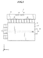
- FIG. 1 is a diagram showing the whole configuration of a liquid crystal display apparatus 1 according to the present embodiment
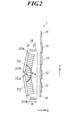
- FIG. 2 is a side view of the liquid crystal display apparatus 1 shown in FIG. 1 .
- the liquid crystal display apparatus 1 comprises a liquid crystal panel 10, and a backlight device 20 which is disposed in the rear of the liquid crystal panel 10.
- a width direction of the liquid crystal panel 10, a height direction thereof, and a depth direction thereof are referred respectively to as X direction, Y direction, and Z direction.
- the liquid crystal panel 10 is a known liquid crystal display panel which is applied to various types of liquid crystal displays (LCDs).
- the liquid crystal panel 10 is exemplified by a display panel which comprises a liquid crystal layer formed by filling liquid crystal in between two glass substrates, and further comprises a polarizing plate which is disposed at an opposite surface of the liquid crystal layer of the both glass substrates.
- the liquid crystal panel 10 may be displayed in colors or in black-and-white, and is not particularly limited with regard to the type of liquid crystal, a liquid crystal cell, a driving section (a switching element) such as a thin film transistor (TFT), a black matrix (BM), and the like.
- a switching element such as a thin film transistor (TFT), a black matrix (BM), and the like.
- TFT thin film transistor
- BM black matrix
- any type of operation modes such as a twisted nematic (TN) mode, a super twisted nematic (STN) mode, an electrically controlled birefringence (ECB) mode, an in-plane switching (IPS) mode, a multidomain vertical alignment (MVA) mode, and the like, is applicable.
- TN twisted nematic
- STN super twisted nematic
- ECB electrically controlled birefringence
- IPS in-plane switching
- MVA multidomain vertical alignment
- the liquid crystal panel 10 further comprises a plurality of source drivers 11 to drive a source wire (a signal line) of the liquid crystal panel 10, and a plurality of gate drivers 12 to drive a gate wire (a scan line) of the liquid crystal panel 10.
- a substrate 15 is connected to the liquid crystal panel 10, wherein the substrate 15 comprises a timing controller 13 to supply various timing signals to the source drivers 11 and to the gate drivers 12, and to receive display data from an external section so as to supply the received display data to the source drivers 11, and a power supply circuit 14 to generate operating voltage of each circuit and driving voltage of the liquid crystal cell.
- Each of the source drivers 11 drives a plurality of source wires of the liquid crystal panel 10, and by being provided with a plurality of source drivers 11, all of the source wires of the liquid crystal panel 10 can be driven. Further, in the same manner as the source drivers 11, each of the gate drivers 12 drives a plurality of gate wires of the liquid crystal panel 10, and by being provided with a plurality of gate drivers 12, all of the gate wires of the liquid crystal panel 10 can be driven.
- driving voltage for one horizontal line is respectively output to all of the source wires at every one horizontal period by the plurality of source drivers 11, and one gate wire is sequentially driven at every one horizontal period by the plurality of gate drivers 12.
- driving voltage for one horizontal line is respectively output to all of the source wires at every one horizontal period by the plurality of source drivers 11, and one gate wire is sequentially driven at every one horizontal period by the plurality of gate drivers 12.
- the backlight device 20 comprises a light emitting section 21 to irradiate a light to the liquid crystal panel 10, and a diffuser plate 22 which is disposed in front of the light emitting section 21 (a liquid crystal panel 10 side) so as to diffuse the light irradiated by the light emitting section 21.
- the light emitting section 21 is configured in a state where two surface light emitters 211, 212 are arranged and disposed one above the other having a predetermined gap H 1 so that the liquid crystal panel 10 is divided into two parts in the Y direction.
- the surface light emitters 211, 212 are not particularly limited, however, an organic EL light emitting panel which comprises three kinds of organic EL light emitting layers to emit three primary colors of R (red), G (green), and B (blue), and selectively emits the three primary colors of R, G, and B by the application of voltage, can be named as one of the surface light emitter, for example.
- the concrete configuration of the organic EL light emitting panel may be as follows. That is to say, the organic EL light emitting panel may comprise, for example, a light transmissive substrate which can transmit a light, a first electrode layer which is formed on the light transmissive substrate and is transparent, three kinds of organic EL light emitting layers which are formed on the first electrode layer in a state of being divided with each other to emit three primary colors of R, G, and B, and a second electrode layer which is formed on the organic EL light emitting layers.
- the two surface light emitters 211, 212 are disposed so that the angle ( ⁇ all ) between their light irradiation surfaces 211A and 212A is smaller than 180 degrees.
- the two surface light emitters 211, 212 are placed so as to satisfy the conditions described in detail hereinbelow.
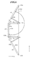
- FIG. 3 is a diagram showing the frame format of a shape of the light emitting section 21 (surface light emitters 211, 212) which is viewed cross-sectionally.
- an intersecting point formed by extending two light irradiation surfaces 211A and 212A in the gap H 1 direction is an intersecting point P1.
- a crossing point formed by perpendicular lines which are respectively perpendicular to the light irradiation surfaces 211A and 212A which extend from edge sections 211b and 212a at the gap H 1 side of the two light irradiation surfaces 211A and 212A is a crossing point P2.
- a hypothetical plane surface which passes the crossing point P2 and which is parallel to the diffuser plate 22 is a hypothetical plane surface L. Moreover, the distance from the intersecting point P 1 to the hypothetical plane surface L is a line segment X 1 .
- a line segment Y 1 distances from the edge sections 211b and 212a of the light irradiation surfaces 211A and 212A to the intersecting point P1 are respectively, a line segment Y 1 , and a line segment Y 2 .
- the angle between the line segments X 1 and Y 1 , and the angle between the line segments X 1 and Y 2 are respectively, ⁇ 1 and ⁇ 2 .
- the diffuser plate 22 is disposed in front of the hypothetical plane surface L at a position which is apart from the hypothetical plane surface L by a predetermined distance D.
- the lights irradiated out from the surface light emitters 211, 212 of the light emitting section 21 are diffused to be approximately even while transmitting inside of the diffuser plate 22 so as to reach the liquid crystal panel 10.
- the diffuser plate 22 is not particularly limited, however, a diffuser plate formed by evenly dispersing a glass fiber having a different refraction index from that of a transparent polycarbonate resin substrate to the resin substrate, or a diffuser plate formed by forming unevenness with suitable roughness on one surface of a transparent glass substrate, can be named as the diffuser plate 22.
- the lights irradiated to the diffuser plate 22 by the light emission of the light emitting section 21 are to satisfy the above formula (3). Thereby, the lights are to intensify each other at the shortest distance at the crossing point P2, before reaching the diffuser plate 22. That is to say, the lights irradiated from the two surface light emitters 211, 212 are to intensify each other at a position corresponding to the gap H 1 of the two surface light emitters 211, 212.
- the lights irradiated out from the two surface light emitters 211, 212 intensify each other at a position corresponding to the gap H 1 of the two surface light emitters 211, 212 before reaching the diffuser plate 22.
- a dark section generated in the liquid crystal panel 10 due to the gap H 1 of the surface light emitters 211, 212 is vanished, and a bright section is generated, and is to be even by the diffuser plate 22.
- the generation of the luminance unevenness in the liquid crystal panel 10 can be reduced.
- the diffuser plate 22 is to be disposed at a position apart from the hypothetical plane surface L by the predetermined distance D in the present embodiment.
- the back surface of the diffuser plate 22 may be overlapped with the hypothetical plane surface L.
- the hypothetical plane surface L is connected to at least one of the edge section 211a of the light irradiation surface 211A and the edge section 212b of the light irradiation surface 212A.
- the thickness of the backlight device 20 can be reduced to the minimum amount.
- FIG. 4 is a top plan view showing a light emitting section 31 of a backlight device 30 in the embodiment 2.
- FIG. 5A is a side view of the backlight device 30, and
- FIG. 5B is a bottom plan view of the backlight device 30.
- the light emitting section 31 of the backlight device 30 is formed by comprising nine surface light emitters 311, 312, ..., 319, each having a rectangular shape.
- the light emitting section 31 is configured in a state where nine surface light emitters 311, ..., are arranged and disposed so that there are three pieces each in the vertical and horizontal directions, and so that the X direction and the Y direction of the liquid crystal panel 10 are respectively divided into three parts.
- the gaps in between the three pieces of the surface light emitters 311, ... in the X direction are W 1 , and W 2 .
- the gaps in between the three pieces of the surface light emitters 311, ... in the Y direction are H 2 , H 3 .
- three pieces of the surface light emitters 311, 312, and 313 arranged in the Y direction are disposed so that the light irradiation surfaces 311A, 312A, and 313A thereof respectively form the angle ⁇ all .
- three pieces of the surface light emitters 311, 314, and 317 arranged in the X direction are disposed so that the light irradiation surfaces 311A, 314A, and 317A thereof respectively form the angle ⁇ all .
- angles ⁇ all and ⁇ all are angles smaller than 180 degrees.
- a distance from the hypothetical plane surface L to the edge section 312a of the lower light irradiation surface 312A is a line segment X 2 .
- a distance from an edge section 311b of the light irradiation surface 311A to the edge section 312a of the light irradiation surface 312A is a line segment Y 3 .
- the angle between the line segments X 2 and Y 3 is ⁇ .
- the angle formed by the light irradiation surfaces 312A, 313A of the lower two surface light emitters 312, 313 is the same as the angle ⁇ , formed by the above described surface light emitters 311, 312.
- the lights irradiated out from the nine surface light emitters 311, ... intensify each other at positions corresponding to the gaps W 1 and W 2 in the X direction, and the gaps H 2 and H 3 in the Y direction of the nine surface light emitters 311, ..., before reaching the diffuser plate 22.
- a dark section generated in the liquid crystal panel 10 is vanished, and a bright section is generated, and is to be even by the diffuser plate 22.
- the generation of the luminance unevenness in the liquid crystal panel 10 can be reduced.
- the conditions are set from the relationship of how the adjacent three surface light emitters are disposed.
- the conditions may be set from the relationship of how the adjacent two surface light emitters are disposed by using the formula (3) described in embodiment 1.
- the surface light emitter is an organic EL is used was explained, but it is not particularly limited to this, as long as the light source is of a surface state.
- a backlight device comprising:
- the backlight device satisfies ⁇ 1 + ⁇ 2 ⁇ COS -1 (Y 1 /X) + COS -1 (Y 2 /X), wherein a distance from a hypothetical plane surface which is parallel to the diffuser plate to an intersecting point formed by extending the two light irradiation surfaces in a gap direction is a line segment X, the hypothetical plane surface passing a crossing point formed by perpendicular lines which are respectively perpendicular to the light irradiation surfaces and which extend from edge sections at a gap side of the two light irradiation surfaces, wherein distances from the two light irradiation surfaces to the intersecting point are respectively, a line segment Y 1 and a line segment Y 2 , and wherein angles formed by the line segments X and Y 1 , and by the line segments X and Y 2 are respectively, ⁇ 1 and ⁇ 2 .
- a liquid crystal display apparatus comprises:
- an angle between the light irradiation surfaces of the two adjacent surface light emitters is configured to be smaller than 180 degrees, thereby lights irradiated out from the light irradiation surfaces of the two adjacent surface light emitters intensify each other.
- a dark section generated in the gap of the adjacent surface light emitters is vanished, and a bright section is generated, and is to be even by the diffuser plate. Therefore, the luminance unevenness in the liquid crystal panel can be prevented.
Landscapes
- Physics & Mathematics (AREA)
- Nonlinear Science (AREA)
- Mathematical Physics (AREA)
- Chemical & Material Sciences (AREA)
- Crystallography & Structural Chemistry (AREA)
- General Physics & Mathematics (AREA)
- Optics & Photonics (AREA)
- Liquid Crystal (AREA)
- Planar Illumination Modules (AREA)
- Electroluminescent Light Sources (AREA)
- Devices For Indicating Variable Information By Combining Individual Elements (AREA)
Abstract
Description
- The present invention relates to a backlight device and a liquid crystal display apparatus.
- Conventionally, a liquid crystal display apparatus comprising a liquid crystal panel, and a backlight device to irradiate a light to the liquid crystal display apparatus, wherein the light emitted from the backlight device is selectively transmitted in the liquid crystal panel so that an image is formed by the transmitted light, is known (see for example, Japanese Patent Application Laid-open Publication Nos.
2002-270019 2004-109205 - As the light source of the backlight device in the liquid crystal display apparatus, light sources using a line light source such as a cold cathode fluorescent lamp (CCFL) or a point light source such as a light emitting diode (LED) have been a mainstream. However, in recent years, developments for a liquid crystal display apparatus using a surface light emitter which is typified by an organic electroluminescence (hereinbelow referred to as an organic EL), and the like, as a light source to realize the thinning and the weight saving, have been in progress.
- In the liquid crystal display apparatus using the surface light emitter, generally, a plurality of surface light emitters are arranged and disposed in a state of each having a predetermined gap in between so as to form a light emitting section, and a liquid crystal panel is disposed in front of the light emitting section.
- However, in the above mentioned liquid crystal display apparatus using the surface light emitters, there has been a problem in that a dark section is generated in the gaps of the adjacent surface light emitters, which results in a generation of luminance unevenness in the liquid crystal panel.
- The objects of the present invention include preventing the luminance unevenness in a backlight device using a surface light emitter, and providing a liquid crystal display apparatus comprising the backlight device.
- According to an aspect of the present invention, there is provided a backlight device comprising:
- a light emitting section including a plurality of surface light emitters which are arranged and disposed so as to have a predetermined gap; and
- a diffuser plate which is disposed in front of the light emitting section to diffuse a light irradiated from the light emitting section, wherein
- an angle between two light irradiation surfaces in the adjacent surface light emitters is smaller than 180 degrees.
- The above and other objects, advantages and features of the present invention will become more fully understood from the detailed description given hereinbelow and the appended drawings which are given by way of illustration only, and thus are not intended as a definition of the limits of the present invention, and wherein:
-
FIG. 1 is a configuration diagram showing the whole configuration of a liquid crystal display apparatus ofembodiment 1 according to the present invention; -
FIG. 2 is a side view of the liquid crystal display apparatus shown inFIG. 1 ; -
FIG. 3 is a view showing a frame format of a backlight device shown inFIG. 2 so as to describe the configuration thereof; -
FIG. 4 is a top plan view showing a light emitting section of a backlight device comprised by a liquid crystal display apparatus ofembodiment 2 according to the present invention; -
FIG. 5A is a side view of the backlight device shown inFIG. 4 ; -
FIG. 5B is a bottom plan view of the backlight device shown inFIG. 4 ; and -
FIG. 6 is a view showing a frame format of the backlight device shown inFIGS. 5A and 5B so as to describe the configuration thereof. - In the following, an
embodiment 1 of the present invention is described with reference to the drawings. However, the scope of the invention is not limited to the illustrated examples. -
FIG. 1 is a diagram showing the whole configuration of a liquidcrystal display apparatus 1 according to the present embodiment, andFIG. 2 is a side view of the liquidcrystal display apparatus 1 shown inFIG. 1 . - The liquid
crystal display apparatus 1 comprises aliquid crystal panel 10, and abacklight device 20 which is disposed in the rear of theliquid crystal panel 10. - In the following, a width direction of the
liquid crystal panel 10, a height direction thereof, and a depth direction thereof are referred respectively to as X direction, Y direction, and Z direction. - The
liquid crystal panel 10 is a known liquid crystal display panel which is applied to various types of liquid crystal displays (LCDs). For example, theliquid crystal panel 10 is exemplified by a display panel which comprises a liquid crystal layer formed by filling liquid crystal in between two glass substrates, and further comprises a polarizing plate which is disposed at an opposite surface of the liquid crystal layer of the both glass substrates. - Further, the
liquid crystal panel 10 may be displayed in colors or in black-and-white, and is not particularly limited with regard to the type of liquid crystal, a liquid crystal cell, a driving section (a switching element) such as a thin film transistor (TFT), a black matrix (BM), and the like. Further, with respect to operation modes, any type of operation modes, such as a twisted nematic (TN) mode, a super twisted nematic (STN) mode, an electrically controlled birefringence (ECB) mode, an in-plane switching (IPS) mode, a multidomain vertical alignment (MVA) mode, and the like, is applicable. - The
liquid crystal panel 10 further comprises a plurality ofsource drivers 11 to drive a source wire (a signal line) of theliquid crystal panel 10, and a plurality ofgate drivers 12 to drive a gate wire (a scan line) of theliquid crystal panel 10. Further, asubstrate 15 is connected to theliquid crystal panel 10, wherein thesubstrate 15 comprises atiming controller 13 to supply various timing signals to thesource drivers 11 and to thegate drivers 12, and to receive display data from an external section so as to supply the received display data to thesource drivers 11, and apower supply circuit 14 to generate operating voltage of each circuit and driving voltage of the liquid crystal cell. - Each of the
source drivers 11 drives a plurality of source wires of theliquid crystal panel 10, and by being provided with a plurality ofsource drivers 11, all of the source wires of theliquid crystal panel 10 can be driven. Further, in the same manner as thesource drivers 11, each of thegate drivers 12 drives a plurality of gate wires of theliquid crystal panel 10, and by being provided with a plurality ofgate drivers 12, all of the gate wires of theliquid crystal panel 10 can be driven. - Further, driving voltage for one horizontal line is respectively output to all of the source wires at every one horizontal period by the plurality of
source drivers 11, and one gate wire is sequentially driven at every one horizontal period by the plurality ofgate drivers 12. Thereby, a liquid crystal cell for one horizontal line in which the source wire and the gate wire intersects, is sequentially driven so as to perform a display operation. - The
backlight device 20 comprises alight emitting section 21 to irradiate a light to theliquid crystal panel 10, and adiffuser plate 22 which is disposed in front of the light emitting section 21 (aliquid crystal panel 10 side) so as to diffuse the light irradiated by thelight emitting section 21. - The
light emitting section 21 according to the present embodiment is configured in a state where two surface light emitters 211, 212 are arranged and disposed one above the other having a predetermined gap H1 so that theliquid crystal panel 10 is divided into two parts in the Y direction. - The surface light emitters 211, 212 are not particularly limited, however, an organic EL light emitting panel which comprises three kinds of organic EL light emitting layers to emit three primary colors of R (red), G (green), and B (blue), and selectively emits the three primary colors of R, G, and B by the application of voltage, can be named as one of the surface light emitter, for example.
- The concrete configuration of the organic EL light emitting panel may be as follows. That is to say, the organic EL light emitting panel may comprise, for example, a light transmissive substrate which can transmit a light, a first electrode layer which is formed on the light transmissive substrate and is transparent, three kinds of organic EL light emitting layers which are formed on the first electrode layer in a state of being divided with each other to emit three primary colors of R, G, and B, and a second electrode layer which is formed on the organic EL light emitting layers.
- As shown in
FIG. 2 , the twosurface light emitters light irradiation surfaces - To put it more concretely, the two
surface light emitters -
FIG. 3 is a diagram showing the frame format of a shape of the light emitting section 21 (surface light emitters 211, 212) which is viewed cross-sectionally. - In
FIG. 3 , an intersecting point formed by extending twolight irradiation surfaces light irradiation surfaces edge sections light irradiation surfaces - Further, a hypothetical plane surface which passes the crossing point P2 and which is parallel to the
diffuser plate 22 is a hypothetical plane surface L. Moreover, the distance from the intersecting point P1 to the hypothetical plane surface L is a line segment X1. - Further, distances from the
edge sections light irradiation surfaces - In this regard, a relationship described in the following formula (1) is realized.

- That is to say, the formula (1) is led to the following formula (2).

- Further, as a condition so that the lights irradiated from the two
surface light emitters 

- When the above formula (3) is satisfied, lights irradiated out from the
lower edge section 211b of thelight irradiation surface 211A and from theupper edge section 212a of thelight irradiation surface 212A are to be crossed at P2. - The
diffuser plate 22 is disposed in front of the hypothetical plane surface L at a position which is apart from the hypothetical plane surface L by a predetermined distance D. - The lights irradiated out from the surface
light emitters light emitting section 21 are diffused to be approximately even while transmitting inside of thediffuser plate 22 so as to reach theliquid crystal panel 10. - The
diffuser plate 22 is not particularly limited, however, a diffuser plate formed by evenly dispersing a glass fiber having a different refraction index from that of a transparent polycarbonate resin substrate to the resin substrate, or a diffuser plate formed by forming unevenness with suitable roughness on one surface of a transparent glass substrate, can be named as thediffuser plate 22. - Next, an operation of the present embodiment is described.
- According to the
backlight device 20 of the present embodiment, the lights irradiated to thediffuser plate 22 by the light emission of thelight emitting section 21 are to satisfy the above formula (3). Thereby, the lights are to intensify each other at the shortest distance at the crossing point P2, before reaching thediffuser plate 22. That is to say, the lights irradiated from the two surfacelight emitters light emitters - Here, the longer the distance of the line segment X1 is, the smaller the angle (θall) between the light irradiation surfaces 211A and 212A of the two surface
light emitters light emitters - As described above, according to the liquid
crystal display apparatus 1 according to the present embodiment, the lights irradiated out from the two surfacelight emitters light emitters diffuser plate 22. Thereby, a dark section generated in theliquid crystal panel 10 due to the gap H1 of the surfacelight emitters diffuser plate 22. Thus, the generation of the luminance unevenness in theliquid crystal panel 10 can be reduced. - Incidentally, the
diffuser plate 22 is to be disposed at a position apart from the hypothetical plane surface L by the predetermined distance D in the present embodiment. However, the back surface of thediffuser plate 22 may be overlapped with the hypothetical plane surface L. - Further, it is preferable that the hypothetical plane surface L is connected to at least one of the
edge section 211a of thelight irradiation surface 211A and theedge section 212b of thelight irradiation surface 212A. - In a case where the above conditions are satisfied, the thickness of the
backlight device 20 can be reduced to the minimum amount. - Next, an
embodiment 2 of the present invention is described, the description of which is mainly given to parts different from theembodiment 1. Incidentally, the sections which are the same as those in theembodiment 1 are allotted with the same reference numbers so as to omit the description thereof. -
FIG. 4 is a top plan view showing alight emitting section 31 of abacklight device 30 in theembodiment 2.FIG. 5A is a side view of thebacklight device 30, andFIG. 5B is a bottom plan view of thebacklight device 30. - As shown in
FIG. 4 , thelight emitting section 31 of thebacklight device 30 according to the present embodiment is formed by comprising nine surfacelight emitters - To put it more concretely, the
light emitting section 31 is configured in a state where nine surfacelight emitters 311, ..., are arranged and disposed so that there are three pieces each in the vertical and horizontal directions, and so that the X direction and the Y direction of theliquid crystal panel 10 are respectively divided into three parts. Here, the gaps in between the three pieces of the surfacelight emitters 311, ... in the X direction are W1, and W2. Further, the gaps in between the three pieces of the surfacelight emitters 311, ... in the Y direction are H2, H3. - As shown in
FIG. 5A , three pieces of the surfacelight emitters - Further, as shown in
FIG. 5B , three pieces of the surfacelight emitters - In this regard, the angles αall and βall are angles smaller than 180 degrees.
- To put it more concretely, the surface light emitters are placed so as to satisfy the conditions described in detail hereinbelow.
-
FIG. 6 is a diagram showing the frame format of a shape of the three surfacelight emitters - In
FIG. 6 , a crossing point formed by perpendicular lines which are respectively perpendicular to the light irradiation surfaces 311A and 312A which extend fromedge sections light emitters - Further, a hypothetical plane surface which passes the crossing point P4 and which is parallel to the
diffuser plate 22 is a hypothetical plane surface L. - Further, a distance from the hypothetical plane surface L to the
edge section 312a of the lowerlight irradiation surface 312A is a line segment X2. A distance from anedge section 311b of thelight irradiation surface 311A to theedge section 312a of thelight irradiation surface 312A is a line segment Y3. Further, the angle between the line segments X2 and Y3 is α. - In this regard, a relationship described in the following formula (4) is realized.


- Further, as a condition so that the lights irradiated from the adjacent surface
light emitters liquid crystal panel 10, the following formula (6) is to be realized.

- Further, the angle formed by the light irradiation surfaces 312A, 313A of the lower two surface
light emitters light emitters - Incidentally, the above formula (6) is a case where α = θ1 and θ2 = 90 degrees are satisfied in the formula (3).
- Further, the above formula (6) is also applicable to βall.
- By setting the surface light emitters in the above described manner, the lights irradiated out from the nine surface
light emitters 311, ..., intensify each other at positions corresponding to the gaps W1 and W2 in the X direction, and the gaps H2 and H3 in the Y direction of the nine surfacelight emitters 311, ..., before reaching thediffuser plate 22. Thereby, a dark section generated in theliquid crystal panel 10 is vanished, and a bright section is generated, and is to be even by thediffuser plate 22. Thus, the generation of the luminance unevenness in theliquid crystal panel 10 can be reduced. - Incidentally, in the present embodiment, the conditions are set from the relationship of how the adjacent three surface light emitters are disposed. However, the conditions may be set from the relationship of how the adjacent two surface light emitters are disposed by using the formula (3) described in
embodiment 1. - Further, it is preferable that the hypothetical plane surface L is connected to at least one of the
edge section 311a of thelight irradiation surface 311A and theedge section 313b of thelight irradiation surface 313A. - In a case where the above conditions are satisfied, the thickness of the
backlight device 30 can be reduced to the minimum amount. - Further, in the
above embodiments - Further, the case where the surface light emitter is an organic EL is used was explained, but it is not particularly limited to this, as long as the light source is of a surface state.
- Moreover, the present invention can of course be suitably modified without being limited from the above described embodiments.
- According to an aspect of the preferred embodiments of the present invention, there is provided a backlight device comprising:
- a light emitting section including a plurality of surface light emitters which are arranged and disposed so as to have a predetermined gap; and
- a diffuser plate which is disposed in front of the light emitting section to diffuse a light irradiated from the light emitting section, wherein
- an angle between two light irradiation surfaces in the adjacent surface light emitters is smaller than 180 degrees.
- Preferably, the backlight device satisfies
θ 1 + θ2 ≤ COS-1 (Y1/X) + COS-1 (Y2/X), wherein
a distance from a hypothetical plane surface which is parallel to the diffuser plate to an intersecting point formed by extending the two light irradiation surfaces in a gap direction is a line segment X, the hypothetical plane surface passing a crossing point formed by perpendicular lines which are respectively perpendicular to the light irradiation surfaces and which extend from edge sections at a gap side of the two light irradiation surfaces, wherein
distances from the two light irradiation surfaces to the intersecting point are respectively, a line segment Y1 and a line segment Y2, and wherein
angles formed by the line segments X and Y1, and by the line segments X and Y2 are respectively, θ1 and θ2. - Preferably, a liquid crystal display apparatus comprises:
- the backlight device; and
- a liquid crystal panel disposed in a light irradiation surface side of the light emitting section of the backlight device.
- According to the preferred embodiments of the present invention, an angle between the light irradiation surfaces of the two adjacent surface light emitters is configured to be smaller than 180 degrees, thereby lights irradiated out from the light irradiation surfaces of the two adjacent surface light emitters intensify each other. Thus, a dark section generated in the gap of the adjacent surface light emitters is vanished, and a bright section is generated, and is to be even by the diffuser plate. Therefore, the luminance unevenness in the liquid crystal panel can be prevented.
- The entire disclosure of Japanese Patent Application No.
2008-122874 filed on May 9, 2008 - Although various exemplary embodiments have been shown and described, the invention is not limited to the embodiments shown. Therefore, the scope of the invention is intended to be limited solely by the scope of the claims that follow.
Claims (3)
- A backlight device comprising:a light emitting section including a plurality of surface light emitters which are arranged and disposed so as to have a predetermined gap; anda diffuser plate which is disposed in front of the light emitting section to diffuse a light irradiated from the light emitting section, whereinan angle between two light irradiation surfaces in the adjacent surface light emitters is smaller than 180 degrees.
- The backlight device according to claim 1, which satisfies
θ 1 + θ2 ≤ COS-1 (Y1/X) + COS-1 (Y2/X), wherein
a distance from a hypothetical plane surface which is parallel to the diffuser plate to an intersecting point formed by extending the two light irradiation surfaces in a gap direction is a line segment X, the hypothetical plane surface passing a crossing point formed by perpendicular lines which are respectively perpendicular to the light irradiation surfaces and which extend from edge sections at a gap side of the two light irradiation surfaces, wherein
distances from the two light irradiation surfaces to the intersecting point are respectively, a line segment Y1 and a line segment Y2, and wherein
angles formed by the line segments X and Y1, and by the line segments X and Y2 are respectively, θ1 and θ2. - A liquid crystal display apparatus comprising:the backlight device according to claim 1 or 2; anda liquid crystal panel disposed in a light irradiation surface side of the light emitting section of the backlight device.
Applications Claiming Priority (1)
| Application Number | Priority Date | Filing Date | Title |
|---|---|---|---|
| JP2008122874A JP2009272193A (en) | 2008-05-09 | 2008-05-09 | Backlight apparatus and liquid crystal display device |
Publications (3)
| Publication Number | Publication Date |
|---|---|
| EP2116893A2 true EP2116893A2 (en) | 2009-11-11 |
| EP2116893A3 EP2116893A3 (en) | 2011-10-05 |
| EP2116893B1 EP2116893B1 (en) | 2016-11-23 |
Family
ID=40902754
Family Applications (1)
| Application Number | Title | Priority Date | Filing Date |
|---|---|---|---|
| EP09159479.6A Not-in-force EP2116893B1 (en) | 2008-05-09 | 2009-05-06 | Backlight device and liquid crystal display apparatus |
Country Status (3)
| Country | Link |
|---|---|
| US (1) | US8773611B2 (en) |
| EP (1) | EP2116893B1 (en) |
| JP (1) | JP2009272193A (en) |
Citations (2)
| Publication number | Priority date | Publication date | Assignee | Title |
|---|---|---|---|---|
| JP2002270019A (en) | 2001-03-07 | 2002-09-20 | Alpine Electronics Inc | Illumination device |
| JP2004109205A (en) | 2002-09-13 | 2004-04-08 | Kodama Chemical Industry Co Ltd | Reflector for direct backlight of liquid crystal display |
Family Cites Families (14)
| Publication number | Priority date | Publication date | Assignee | Title |
|---|---|---|---|---|
| DE60236480D1 (en) * | 2001-03-29 | 2010-07-08 | Panasonic Corp | Image reader |
| US7362046B2 (en) * | 2001-11-10 | 2008-04-22 | Image Portal Limited | Partial overlapping display tiles of organic light emitting device |
| KR100783592B1 (en) * | 2002-02-05 | 2007-12-07 | 삼성전자주식회사 | Lighting device and display device using it as backlight |
| US7271534B2 (en) * | 2003-11-04 | 2007-09-18 | 3M Innovative Properties Company | Segmented organic light emitting device |
| KR20070045287A (en) * | 2004-08-24 | 2007-05-02 | 니폰 제온 가부시키가이샤 | Direct-under backlight |
| JP2006147549A (en) * | 2004-10-19 | 2006-06-08 | Showa Denko Kk | Planar light emitter, manufacturing method and use thereof |
| TWI288851B (en) * | 2005-03-09 | 2007-10-21 | Hannstar Display Corp | Backlight source module |
| KR101093324B1 (en) * | 2005-05-30 | 2011-12-14 | 엘지이노텍 주식회사 | Backlight unit with light emitting diode |
| JP2007171681A (en) * | 2005-12-22 | 2007-07-05 | Infovision Optoelectronics Holdings Ltd | Backlight used for curved liquid crystal display device and curved liquid crystal display device |
| JP2009087538A (en) * | 2006-01-20 | 2009-04-23 | Sharp Corp | Light source unit, illumination device using the same, and display device using the same |
| JP2007273275A (en) * | 2006-03-31 | 2007-10-18 | Canon Inc | Organic EL light emitting device |
| JP2007273309A (en) * | 2006-03-31 | 2007-10-18 | Asahi Kasei Chemicals Corp | LED light source and display body using the same |
| KR100799864B1 (en) * | 2006-04-21 | 2008-01-31 | 삼성전기주식회사 | LED Package |
| JP2008021420A (en) * | 2006-07-10 | 2008-01-31 | Minebea Co Ltd | Surface lighting device |
-
2008
- 2008-05-09 JP JP2008122874A patent/JP2009272193A/en active Pending
-
2009
- 2009-05-06 US US12/436,411 patent/US8773611B2/en not_active Expired - Fee Related
- 2009-05-06 EP EP09159479.6A patent/EP2116893B1/en not_active Not-in-force
Patent Citations (2)
| Publication number | Priority date | Publication date | Assignee | Title |
|---|---|---|---|---|
| JP2002270019A (en) | 2001-03-07 | 2002-09-20 | Alpine Electronics Inc | Illumination device |
| JP2004109205A (en) | 2002-09-13 | 2004-04-08 | Kodama Chemical Industry Co Ltd | Reflector for direct backlight of liquid crystal display |
Also Published As
| Publication number | Publication date |
|---|---|
| US20090279019A1 (en) | 2009-11-12 |
| JP2009272193A (en) | 2009-11-19 |
| EP2116893B1 (en) | 2016-11-23 |
| EP2116893A3 (en) | 2011-10-05 |
| US8773611B2 (en) | 2014-07-08 |
Similar Documents
| Publication | Publication Date | Title |
|---|---|---|
| US8199280B2 (en) | Backlight assembly and display device having the same | |
| KR101201307B1 (en) | Back Light Unit | |
| KR101656742B1 (en) | Liquid crystal display device | |
| KR101291940B1 (en) | Transparent display device | |
| US20160282667A1 (en) | Color liquid crystal display module structure and backlight module thereof | |
| US20080144334A1 (en) | Light emitting diode package, and light source unit and backlight unit including the same | |
| KR101338998B1 (en) | Transflective liquid crystal display device | |
| KR20100075134A (en) | Backlight unit for liquid crystal display device | |
| KR100950514B1 (en) | LCD Display | |
| JP2017032782A (en) | Display device | |
| JPWO2016129514A1 (en) | Lighting device and display device | |
| KR101280294B1 (en) | Display device | |
| US20060192747A1 (en) | Liquid crystal display apparatus | |
| EP2116893B1 (en) | Backlight device and liquid crystal display apparatus | |
| KR100505182B1 (en) | Structure of backlignt unit for liquid crystal display | |
| JP4628043B2 (en) | Liquid crystal display device | |
| JP4585989B2 (en) | Backlight, liquid crystal display element | |
| JP4754846B2 (en) | Liquid crystal display | |
| KR100469510B1 (en) | Structure of backlignt unit for liquid crystal display | |
| KR20060000814A (en) | Backlight Unit of LCD | |
| KR100469509B1 (en) | Structure of backlignt unit for liquid crystal display | |
| KR20060109577A (en) | LCD panel | |
| KR101028343B1 (en) | LCD and its driving method | |
| KR102007830B1 (en) | Backlight unit and liquid crystal display device including the same | |
| KR20080020840A (en) | Light source device and liquid crystal display device |
Legal Events
| Date | Code | Title | Description |
|---|---|---|---|
| PUAI | Public reference made under article 153(3) epc to a published international application that has entered the european phase |
Free format text: ORIGINAL CODE: 0009012 |
|
| AK | Designated contracting states |
Kind code of ref document: A2 Designated state(s): AT BE BG CH CY CZ DE DK EE ES FI FR GB GR HR HU IE IS IT LI LT LU LV MC MK MT NL NO PL PT RO SE SI SK TR |
|
| PUAL | Search report despatched |
Free format text: ORIGINAL CODE: 0009013 |
|
| AK | Designated contracting states |
Kind code of ref document: A3 Designated state(s): AT BE BG CH CY CZ DE DK EE ES FI FR GB GR HR HU IE IS IT LI LT LU LV MC MK MT NL NO PL PT RO SE SI SK TR |
|
| AX | Request for extension of the european patent |
Extension state: AL BA RS |
|
| RIC1 | Information provided on ipc code assigned before grant |
Ipc: H01L 27/32 20060101ALI20110829BHEP Ipc: F21S 2/00 20060101ALI20110829BHEP Ipc: G02F 1/13357 20060101AFI20110829BHEP |
|
| 17P | Request for examination filed |
Effective date: 20120405 |
|
| 17Q | First examination report despatched |
Effective date: 20151026 |
|
| GRAP | Despatch of communication of intention to grant a patent |
Free format text: ORIGINAL CODE: EPIDOSNIGR1 |
|
| INTG | Intention to grant announced |
Effective date: 20160610 |
|
| GRAS | Grant fee paid |
Free format text: ORIGINAL CODE: EPIDOSNIGR3 |
|
| GRAA | (expected) grant |
Free format text: ORIGINAL CODE: 0009210 |
|
| AK | Designated contracting states |
Kind code of ref document: B1 Designated state(s): AT BE BG CH CY CZ DE DK EE ES FI FR GB GR HR HU IE IS IT LI LT LU LV MC MK MT NL NO PL PT RO SE SI SK TR |
|
| REG | Reference to a national code |
Ref country code: GB Ref legal event code: FG4D |
|
| REG | Reference to a national code |
Ref country code: CH Ref legal event code: EP |
|
| REG | Reference to a national code |
Ref country code: IE Ref legal event code: FG4D |
|
| REG | Reference to a national code |
Ref country code: AT Ref legal event code: REF Ref document number: 848445 Country of ref document: AT Kind code of ref document: T Effective date: 20161215 |
|
| REG | Reference to a national code |
Ref country code: DE Ref legal event code: R096 Ref document number: 602009042568 Country of ref document: DE |
|
| PG25 | Lapsed in a contracting state [announced via postgrant information from national office to epo] |
Ref country code: LV Free format text: LAPSE BECAUSE OF FAILURE TO SUBMIT A TRANSLATION OF THE DESCRIPTION OR TO PAY THE FEE WITHIN THE PRESCRIBED TIME-LIMIT Effective date: 20161123 |
|
| REG | Reference to a national code |
Ref country code: LT Ref legal event code: MG4D |
|
| REG | Reference to a national code |
Ref country code: NL Ref legal event code: MP Effective date: 20161123 |
|
| REG | Reference to a national code |
Ref country code: AT Ref legal event code: MK05 Ref document number: 848445 Country of ref document: AT Kind code of ref document: T Effective date: 20161123 |
|
| PG25 | Lapsed in a contracting state [announced via postgrant information from national office to epo] |
Ref country code: SE Free format text: LAPSE BECAUSE OF FAILURE TO SUBMIT A TRANSLATION OF THE DESCRIPTION OR TO PAY THE FEE WITHIN THE PRESCRIBED TIME-LIMIT Effective date: 20161123 Ref country code: LT Free format text: LAPSE BECAUSE OF FAILURE TO SUBMIT A TRANSLATION OF THE DESCRIPTION OR TO PAY THE FEE WITHIN THE PRESCRIBED TIME-LIMIT Effective date: 20161123 Ref country code: NO Free format text: LAPSE BECAUSE OF FAILURE TO SUBMIT A TRANSLATION OF THE DESCRIPTION OR TO PAY THE FEE WITHIN THE PRESCRIBED TIME-LIMIT Effective date: 20170223 Ref country code: NL Free format text: LAPSE BECAUSE OF FAILURE TO SUBMIT A TRANSLATION OF THE DESCRIPTION OR TO PAY THE FEE WITHIN THE PRESCRIBED TIME-LIMIT Effective date: 20161123 Ref country code: GR Free format text: LAPSE BECAUSE OF FAILURE TO SUBMIT A TRANSLATION OF THE DESCRIPTION OR TO PAY THE FEE WITHIN THE PRESCRIBED TIME-LIMIT Effective date: 20170224 |
|
| PG25 | Lapsed in a contracting state [announced via postgrant information from national office to epo] |
Ref country code: PT Free format text: LAPSE BECAUSE OF FAILURE TO SUBMIT A TRANSLATION OF THE DESCRIPTION OR TO PAY THE FEE WITHIN THE PRESCRIBED TIME-LIMIT Effective date: 20170323 Ref country code: HR Free format text: LAPSE BECAUSE OF FAILURE TO SUBMIT A TRANSLATION OF THE DESCRIPTION OR TO PAY THE FEE WITHIN THE PRESCRIBED TIME-LIMIT Effective date: 20161123 Ref country code: AT Free format text: LAPSE BECAUSE OF FAILURE TO SUBMIT A TRANSLATION OF THE DESCRIPTION OR TO PAY THE FEE WITHIN THE PRESCRIBED TIME-LIMIT Effective date: 20161123 Ref country code: FI Free format text: LAPSE BECAUSE OF FAILURE TO SUBMIT A TRANSLATION OF THE DESCRIPTION OR TO PAY THE FEE WITHIN THE PRESCRIBED TIME-LIMIT Effective date: 20161123 Ref country code: PL Free format text: LAPSE BECAUSE OF FAILURE TO SUBMIT A TRANSLATION OF THE DESCRIPTION OR TO PAY THE FEE WITHIN THE PRESCRIBED TIME-LIMIT Effective date: 20161123 Ref country code: ES Free format text: LAPSE BECAUSE OF FAILURE TO SUBMIT A TRANSLATION OF THE DESCRIPTION OR TO PAY THE FEE WITHIN THE PRESCRIBED TIME-LIMIT Effective date: 20161123 |
|
| REG | Reference to a national code |
Ref country code: DE Ref legal event code: R084 Ref document number: 602009042568 Country of ref document: DE |
|
| PG25 | Lapsed in a contracting state [announced via postgrant information from national office to epo] |
Ref country code: DK Free format text: LAPSE BECAUSE OF FAILURE TO SUBMIT A TRANSLATION OF THE DESCRIPTION OR TO PAY THE FEE WITHIN THE PRESCRIBED TIME-LIMIT Effective date: 20161123 Ref country code: SK Free format text: LAPSE BECAUSE OF FAILURE TO SUBMIT A TRANSLATION OF THE DESCRIPTION OR TO PAY THE FEE WITHIN THE PRESCRIBED TIME-LIMIT Effective date: 20161123 Ref country code: EE Free format text: LAPSE BECAUSE OF FAILURE TO SUBMIT A TRANSLATION OF THE DESCRIPTION OR TO PAY THE FEE WITHIN THE PRESCRIBED TIME-LIMIT Effective date: 20161123 Ref country code: RO Free format text: LAPSE BECAUSE OF FAILURE TO SUBMIT A TRANSLATION OF THE DESCRIPTION OR TO PAY THE FEE WITHIN THE PRESCRIBED TIME-LIMIT Effective date: 20161123 Ref country code: CZ Free format text: LAPSE BECAUSE OF FAILURE TO SUBMIT A TRANSLATION OF THE DESCRIPTION OR TO PAY THE FEE WITHIN THE PRESCRIBED TIME-LIMIT Effective date: 20161123 |
|
| PGFP | Annual fee paid to national office [announced via postgrant information from national office to epo] |
Ref country code: DE Payment date: 20170502 Year of fee payment: 9 |
|
| REG | Reference to a national code |
Ref country code: DE Ref legal event code: R097 Ref document number: 602009042568 Country of ref document: DE |
|
| PG25 | Lapsed in a contracting state [announced via postgrant information from national office to epo] |
Ref country code: LU Free format text: LAPSE BECAUSE OF NON-PAYMENT OF DUE FEES Effective date: 20170531 Ref country code: BE Free format text: LAPSE BECAUSE OF FAILURE TO SUBMIT A TRANSLATION OF THE DESCRIPTION OR TO PAY THE FEE WITHIN THE PRESCRIBED TIME-LIMIT Effective date: 20161123 Ref country code: BG Free format text: LAPSE BECAUSE OF FAILURE TO SUBMIT A TRANSLATION OF THE DESCRIPTION OR TO PAY THE FEE WITHIN THE PRESCRIBED TIME-LIMIT Effective date: 20170223 Ref country code: IT Free format text: LAPSE BECAUSE OF FAILURE TO SUBMIT A TRANSLATION OF THE DESCRIPTION OR TO PAY THE FEE WITHIN THE PRESCRIBED TIME-LIMIT Effective date: 20161123 |
|
| PLBE | No opposition filed within time limit |
Free format text: ORIGINAL CODE: 0009261 |
|
| STAA | Information on the status of an ep patent application or granted ep patent |
Free format text: STATUS: NO OPPOSITION FILED WITHIN TIME LIMIT |
|
| 26N | No opposition filed |
Effective date: 20170824 |
|
| PG25 | Lapsed in a contracting state [announced via postgrant information from national office to epo] |
Ref country code: SI Free format text: LAPSE BECAUSE OF FAILURE TO SUBMIT A TRANSLATION OF THE DESCRIPTION OR TO PAY THE FEE WITHIN THE PRESCRIBED TIME-LIMIT Effective date: 20161123 |
|
| REG | Reference to a national code |
Ref country code: CH Ref legal event code: PL |
|
| GBPC | Gb: european patent ceased through non-payment of renewal fee |
Effective date: 20170506 |
|
| PG25 | Lapsed in a contracting state [announced via postgrant information from national office to epo] |
Ref country code: MC Free format text: LAPSE BECAUSE OF FAILURE TO SUBMIT A TRANSLATION OF THE DESCRIPTION OR TO PAY THE FEE WITHIN THE PRESCRIBED TIME-LIMIT Effective date: 20161123 |
|
| REG | Reference to a national code |
Ref country code: IE Ref legal event code: MM4A |
|
| PG25 | Lapsed in a contracting state [announced via postgrant information from national office to epo] |
Ref country code: LI Free format text: LAPSE BECAUSE OF NON-PAYMENT OF DUE FEES Effective date: 20170531 Ref country code: CH Free format text: LAPSE BECAUSE OF NON-PAYMENT OF DUE FEES Effective date: 20170531 |
|
| REG | Reference to a national code |
Ref country code: FR Ref legal event code: ST Effective date: 20180131 |
|
| PG25 | Lapsed in a contracting state [announced via postgrant information from national office to epo] |
Ref country code: LU Free format text: LAPSE BECAUSE OF NON-PAYMENT OF DUE FEES Effective date: 20170506 |
|
| PG25 | Lapsed in a contracting state [announced via postgrant information from national office to epo] |
Ref country code: IE Free format text: LAPSE BECAUSE OF NON-PAYMENT OF DUE FEES Effective date: 20170506 Ref country code: GB Free format text: LAPSE BECAUSE OF NON-PAYMENT OF DUE FEES Effective date: 20170506 |
|
| PG25 | Lapsed in a contracting state [announced via postgrant information from national office to epo] |
Ref country code: FR Free format text: LAPSE BECAUSE OF NON-PAYMENT OF DUE FEES Effective date: 20170531 |
|
| PG25 | Lapsed in a contracting state [announced via postgrant information from national office to epo] |
Ref country code: MT Free format text: LAPSE BECAUSE OF NON-PAYMENT OF DUE FEES Effective date: 20170506 |
|
| REG | Reference to a national code |
Ref country code: DE Ref legal event code: R119 Ref document number: 602009042568 Country of ref document: DE |
|
| PG25 | Lapsed in a contracting state [announced via postgrant information from national office to epo] |
Ref country code: DE Free format text: LAPSE BECAUSE OF NON-PAYMENT OF DUE FEES Effective date: 20181201 |
|
| PG25 | Lapsed in a contracting state [announced via postgrant information from national office to epo] |
Ref country code: HU Free format text: LAPSE BECAUSE OF FAILURE TO SUBMIT A TRANSLATION OF THE DESCRIPTION OR TO PAY THE FEE WITHIN THE PRESCRIBED TIME-LIMIT; INVALID AB INITIO Effective date: 20090506 |
|
| PG25 | Lapsed in a contracting state [announced via postgrant information from national office to epo] |
Ref country code: CY Free format text: LAPSE BECAUSE OF NON-PAYMENT OF DUE FEES Effective date: 20161123 |
|
| PG25 | Lapsed in a contracting state [announced via postgrant information from national office to epo] |
Ref country code: MK Free format text: LAPSE BECAUSE OF FAILURE TO SUBMIT A TRANSLATION OF THE DESCRIPTION OR TO PAY THE FEE WITHIN THE PRESCRIBED TIME-LIMIT Effective date: 20161123 |
|
| PG25 | Lapsed in a contracting state [announced via postgrant information from national office to epo] |
Ref country code: TR Free format text: LAPSE BECAUSE OF FAILURE TO SUBMIT A TRANSLATION OF THE DESCRIPTION OR TO PAY THE FEE WITHIN THE PRESCRIBED TIME-LIMIT Effective date: 20161123 |
|
| PG25 | Lapsed in a contracting state [announced via postgrant information from national office to epo] |
Ref country code: IS Free format text: LAPSE BECAUSE OF FAILURE TO SUBMIT A TRANSLATION OF THE DESCRIPTION OR TO PAY THE FEE WITHIN THE PRESCRIBED TIME-LIMIT Effective date: 20170323 |