EP2116872A1 - Multilayer structure formed by nanoparticular lamina with unidimensional photonic crystal properties, method for the production thereof and use thereof - Google Patents
Multilayer structure formed by nanoparticular lamina with unidimensional photonic crystal properties, method for the production thereof and use thereof Download PDFInfo
- Publication number
- EP2116872A1 EP2116872A1 EP08718475A EP08718475A EP2116872A1 EP 2116872 A1 EP2116872 A1 EP 2116872A1 EP 08718475 A EP08718475 A EP 08718475A EP 08718475 A EP08718475 A EP 08718475A EP 2116872 A1 EP2116872 A1 EP 2116872A1
- Authority
- EP
- European Patent Office
- Prior art keywords
- multilayer structure
- nanoparticles
- laminae
- nanoparticulate
- different
- Prior art date
- Legal status (The legal status is an assumption and is not a legal conclusion. Google has not performed a legal analysis and makes no representation as to the accuracy of the status listed.)
- Granted
Links
Images




Classifications
-
- G—PHYSICS
- G02—OPTICS
- G02B—OPTICAL ELEMENTS, SYSTEMS OR APPARATUS
- G02B1/00—Optical elements characterised by the material of which they are made; Optical coatings for optical elements
- G02B1/02—Optical elements characterised by the material of which they are made; Optical coatings for optical elements made of crystals, e.g. rock-salt, semi-conductors
-
- G—PHYSICS
- G02—OPTICS
- G02B—OPTICAL ELEMENTS, SYSTEMS OR APPARATUS
- G02B5/00—Optical elements other than lenses
- G02B5/20—Filters
- G02B5/28—Interference filters
- G02B5/285—Interference filters comprising deposited thin solid films
-
- B—PERFORMING OPERATIONS; TRANSPORTING
- B82—NANOTECHNOLOGY
- B82Y—SPECIFIC USES OR APPLICATIONS OF NANOSTRUCTURES; MEASUREMENT OR ANALYSIS OF NANOSTRUCTURES; MANUFACTURE OR TREATMENT OF NANOSTRUCTURES
- B82Y20/00—Nanooptics, e.g. quantum optics or photonic crystals
-
- G—PHYSICS
- G02—OPTICS
- G02B—OPTICAL ELEMENTS, SYSTEMS OR APPARATUS
- G02B1/00—Optical elements characterised by the material of which they are made; Optical coatings for optical elements
- G02B1/002—Optical elements characterised by the material of which they are made; Optical coatings for optical elements made of materials engineered to provide properties not available in nature, e.g. metamaterials
- G02B1/005—Optical elements characterised by the material of which they are made; Optical coatings for optical elements made of materials engineered to provide properties not available in nature, e.g. metamaterials made of photonic crystals or photonic band gap materials
-
- G—PHYSICS
- G02—OPTICS
- G02B—OPTICAL ELEMENTS, SYSTEMS OR APPARATUS
- G02B5/00—Optical elements other than lenses
- G02B5/20—Filters
- G02B5/28—Interference filters
- G02B5/285—Interference filters comprising deposited thin solid films
- G02B5/286—Interference filters comprising deposited thin solid films having four or fewer layers, e.g. for achieving a colour effect
-
- G—PHYSICS
- G02—OPTICS
- G02B—OPTICAL ELEMENTS, SYSTEMS OR APPARATUS
- G02B2207/00—Coding scheme for general features or characteristics of optical elements and systems of subclass G02B, but not including elements and systems which would be classified in G02B6/00 and subgroups
- G02B2207/107—Porous materials, e.g. for reducing the refractive index
-
- G—PHYSICS
- G02—OPTICS
- G02B—OPTICAL ELEMENTS, SYSTEMS OR APPARATUS
- G02B5/00—Optical elements other than lenses
- G02B5/08—Mirrors
- G02B5/0816—Multilayer mirrors, i.e. having two or more reflecting layers
-
- Y—GENERAL TAGGING OF NEW TECHNOLOGICAL DEVELOPMENTS; GENERAL TAGGING OF CROSS-SECTIONAL TECHNOLOGIES SPANNING OVER SEVERAL SECTIONS OF THE IPC; TECHNICAL SUBJECTS COVERED BY FORMER USPC CROSS-REFERENCE ART COLLECTIONS [XRACs] AND DIGESTS
- Y10—TECHNICAL SUBJECTS COVERED BY FORMER USPC
- Y10T—TECHNICAL SUBJECTS COVERED BY FORMER US CLASSIFICATION
- Y10T428/00—Stock material or miscellaneous articles
- Y10T428/24—Structurally defined web or sheet [e.g., overall dimension, etc.]
- Y10T428/24942—Structurally defined web or sheet [e.g., overall dimension, etc.] including components having same physical characteristic in differing degree
-
- Y—GENERAL TAGGING OF NEW TECHNOLOGICAL DEVELOPMENTS; GENERAL TAGGING OF CROSS-SECTIONAL TECHNOLOGIES SPANNING OVER SEVERAL SECTIONS OF THE IPC; TECHNICAL SUBJECTS COVERED BY FORMER USPC CROSS-REFERENCE ART COLLECTIONS [XRACs] AND DIGESTS
- Y10—TECHNICAL SUBJECTS COVERED BY FORMER USPC
- Y10T—TECHNICAL SUBJECTS COVERED BY FORMER US CLASSIFICATION
- Y10T428/00—Stock material or miscellaneous articles
- Y10T428/24—Structurally defined web or sheet [e.g., overall dimension, etc.]
- Y10T428/24942—Structurally defined web or sheet [e.g., overall dimension, etc.] including components having same physical characteristic in differing degree
- Y10T428/2495—Thickness [relative or absolute]
Definitions
- Materials with a multilayer structure have important applications as optical elements, as they act as interferential filters or Bragg reflectors, capable of selectively reflecting or transmitting a range of electromagnetic frequencies, generally comprised between the ultraviolet and infrared ranges of the spectrum, determined by the thickness and refractive index of the layers.
- these materials are unidimensional photonic crystals, as they have a periodic modulation of the refractive index in one of the three spatial directions.
- the multilayer systems currently available on the market are mostly manufactured using techniques that are normally grouped under the term Physical Vapour Deposition. In all cases, deposition takes place under vacuum conditions and the solid is condensed directly from the vapour phase. Optical coatings obtained through this kind of technique have great stability against variations in ambient conditions, in addition to high mechanical resistance. There is another large group of multilayer formation methods based on sol-gel type processes. These methods have allowed the development of multilayer coatings which are highly resistant to damage caused by intense laser radiations, having much higher damage thresholds than other types of structures.
- these multilayer coatings have low mechanical stability, and their properties vary according to the ambient conditions, both phenomena being related to their mesoporosity, due to which they are not suitable as passive optical elements, even though they do have applications in other fields, such as that of sensors.
- the pores of a layer grown by sol-gel are irregular in shape, with a very wide size distribution and an average size comprised between 2 nm and 100 nm.
- a multilayer structure with a controlled mesostructure (shape and size), the optical properties of which can be controlled, would open new application possibilities for these types of materials in different fields. Materials with relatively controlled mesoporosity and which have aroused much interest, although uses for these have not yet been presented, have also been recently developed.
- Bragg Reflectors or BRs in 1D are the photonic crystals which have achieved greater development due to the sol-gel. Very high reflectivities are obtained in these materials due to the Bragg reflection phenomenon. In general, they are produced by alternating layers of materials with a high and low refractive index, forming a stack of dielectric multilayers.
- BRs synthesised by sol-gel can be obtained by spin-coating [ R.M. Almeida, S. Portal, Photonic band gap structures by sol-gel processing, Current Opinion in Solid State and Materials Science 7 (2003) 151 . R.M. Almeida, A.S.
- Thermal densification treatments are carried out after the synthesis of each of the layers and, on using such high temperatures, crystallisation of the TiO 2 of the first layers cannot be avoided, the first layers being subjected to high temperatures for longer time periods due to the reiterated thermal treatments they undergo.
- porous silicon (pSi) multilayers having different porosity allows the production of structures with a predetermined refractive index profile, which results in a multilayer interferential filter or BR.
- the refractive index of each layer is designed according to its porosity, which is obtained by electrochemical etching of monocrystalline silicon wafers in an ethanolic solution of hydrofluoric acid.
- thickness can also be controlled and, therefore, the optical properties, adjusting synthesis conditions such as acid concentration, current density and etching time.
- a large number of layers without the structural integrity problems of multilayer films obtained by sol-gel in the form of BRs can be obtained, and the thickness and porosity of each layer can be controlled in a very precise manner.
- the main problem of these materials is their long-term altered stability.
- the application of pSi BRs in air or aqueous media generates oxide on the surface in just a few hours, due to which they must be chemically modified to increase their oxidation resistance.
- This type of multilayer is manufactured by the alternating deposition, using spin-coating ( S.Y. Choi, M. Mamak, G. von Freymann, N. Chopra, G.A. Ozin, Mesoporous Bragg Stack Color Tunable Sensors, Nano Letters 6 (2006) 2456 ) or dip-coating techniques (M.C. Fuertes, G. Soler-Illia, H. M ⁇ guez, Spanish patent with application number: 200602405 ), of laminae with ordered mesopores which are obtained using a template or organic mould combined with the compounds that give rise to the inorganic phase in the precursor solution which is deposited to form each layer.
- the porosity of these layers allows modification of their optical response by the infiltration of liquids.
- the possibility of functionalising the mesopore walls in turn allows this response to be selective to a specific type or group of compounds.
- An object of the present invention consists of a mesoporous multilayer structure with the properties of a Bragg reflector or unidimensional photonic crystal, hereinafter referred to as the nanoparticulate multilayer structure of the invention, which comprises periodically alternating laminae with different refractive indices, each of a thickness comprised between 1 nm and 200 nm and composed of nanoparticles.
- the nanoparticulate multilayer structure of the invention is deposited on a substrate during the production process, wherein nanoparticles of several different materials may be used, conferring a different refractive index to each lamina and, therefore, different characteristics to each multilayer structure.
- Another object of the present invention consists of a process for manufacturing the nanoparticulate multilayer structure having unidimensional photonic crystal properties, hereinafter referred to as the process of the invention, which comprises the following stages:
- Another object of the invention is the use of the nanoparticulate multilayer structure of the invention in the preferred production of optical elements to be used, by way of example and without limiting the scope of the invention, preferably, in sensor devices, photoelectrochemical devices, coloured coatings and reflective coatings.
- the present invention is based on the fact that the inventors have observed that it is possible to obtain, from a new process wherein optically uniform nanoparticle laminae are periodically alternating, a new mesoporous multilayer structure (having pores between 1 nm and 100 nm) with an alternating refractive index and high reflectance at different wavelengths.
- a Bragg reflector or unidimensional photonic crystal are observed in the ultraviolet, visible and infrared ranges close to the electromagnetic spectrum.
- This unidimensional photonic crystal formed by laminae having different refractive indices and controlled thickness composed of nanoparticles may be deposited on different types of substrates using a simple and reliable method.
- This periodic multilayer of high interconnected porosity which is accessible from the exterior and has unidimensional photonic crystal properties, is formed through the alternating deposition of laminae of oxide or semiconductor nanoparticles of a controlled thickness, in such a manner that a periodic alternation in the refractive index value is created. This alternation gives rise to the behaviour of the photonic crystal of the multilayer.
- the periodic alternation of laminae having different refractive indices gives rise to high reflectance which can easily be observed with the naked eye and can be measured with a spectrophotometer.
- the mesoporous structure of this reflector is such that it allows the diffusion of liquids therethrough. This gives rise to the possibility of modifying, in a controlled manner, the colour of the multilayer structure in accordance with the infiltrated liquid and is therefore a material which can be used in the manufacturing of a sensor.
- the proven nanoparticulate nature of each layer that forms the multilayer implies a significant qualitative structural difference with respect to mesoporous multilayers manufactured in the past.
- an object of the present invention consists of a mesoporous multilayer structure with the properties of a Bragg reflector or unidimensional photonic crystal, hereinafter referred to as nanoparticulate multilayer structure of the invention, which comprises periodically alternating laminae with different refractive indices, each of a thickness comprised between 1 nm and 200 nm and composed of nanoparticles.
- the nanoparticulate multilayer structure of the invention is deposited on a substrate during the production process, wherein nanoparticles of several different materials may be used, conferring a different refractive index to each lamina and, therefore, different characteristics to each multilayer structure.
- a specific object of the present invention consists of the nanoparticulate multilayer structure of the invention, which comprises laminae with nanoparticles of different materials (Example 2, Figure3 ).
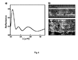
- Another specific object of the present invention consists of the nanoparticulate multilayer structure of the invention, which comprises laminae with nanoparticles of the same material (Example 3, Figure 4 ).
- the nanoparticles present in the nanoparticulate multilayer structure of the invention may be of any material that can be obtained in the form of nanoparticles of a size comprised between 1 nm and 100 nm, and which allow the desired refractive index contrast between the laminae to be obtained.
- the nanoparticle material by way of an example and without limiting the scope of the invention, belongs to the following group: metal oxides, metal halides, nitrides, carbides, chalcogenides, metals, semiconductors, polymers or a combination thereof.
- the oxides are selected from the group of inorganic oxides both in their amorphous or crystalline phase; and most preferably, these materials are selected from the group: SiO 2 , TiO 2 , SnO 2 , ZnO, Nb 2 O 5 , CeO 2 , Fe 2 O 3 , Fe 3 O 4 , V 2 O 5 , Cr 2 O 3 , HfO 2 , MnO 2 , Mn 2 O 3 , CO 3 O 4 , NiO, Al 2 O 3 , In 2 O 3 , SnO 2 .
- a particular embodiment of this invention consists of a nanoparticulate multilayer structure, wherein the selected nanoparticules are of a material belonging to the following groups: SiO 2 /TiO 2 and SiO 2 /SnO 2 . Examples of structures composed of these nanoparticles are shown in Examples 1, 2, 4, 5 and 6.
- Another particular object of the present invention consists of the nanoparticulate multilayer structure of the invention, which comprises laminae with nanoparticles, of the same or different material, but with a different distribution of nanoparticle sizes.
- the difference or equivalence in nanoparticle size determines different porosity and confers a different refractive index to each layer.
- a particular embodiment consists of a nanoparticulate multilayer structure of the invention, which comprises laminae with nanoparticles, of the same material, such as for example TiO 2 , but with a different nanoparticle size distribution (Example 3, Figure 4 ).
- Another object of the present invention consists of the nanoparticulate multilayer structure of the invention, which comprises one or several ruptures in the periodicity of the laminae.
- This nanoparticulate multilayer structure has a spatial periodicity interrupted by the presence of a lamina of greater depth or thickness with respect to those that form the periodicity, in such a manner that default optical states are generated in the unidimensional photonic crystal.
- This nanoparticulate multilayer structure of the invention with periodicity rupture or interruption can also be extended through the inclusion of laminae of different thicknesses, for example between 1 nm and 200 nm, formed of nanoparticles of different material and size and, therefore, porosity.
- Another object of the present invention consists of a manufacturing process of the nanoparticulate multilayer structure with unidimensional photonic crystal properties, hereinafter referred to as process of the invention, which comprises the following stages:
- the nanoparticles of the process of the invention may be of any material that can be obtained in the form of nanoparticles of a size comprised between 1 nm and 100 nm.
- the materials used in the form of nanoparticles (or a combination thereof) for the deposition of the multilayer structure with photonic crystal properties will be those which allow the desired refractive index contrast between the layers to be obtained.
- the composition can be that of any of the metal oxides, metal halides, nitrides, carbides, chalcogenides, metals, semiconductors, polymers or a combination thereof.
- these materials are selected from the group: SiO 2 , TiO 2 , SnO 2 , ZnO, Nb 2 O 5 , CeO 2 , Fe 2 O 3 , Fe 3 O 4 , V 2 O 5 , Cr 2 O 3 , HfO 2 , MnO 2 , Mn 2 O 3 , Co 3 O 4 , NiO, Al 2 O 3 , In 2 O 3 , SnO 2 .
- the selected nanoparticles are of the materials SiO 2 , TiO 2 and SnO 2 . Examples of structures composed of these nanoparticles are shown in examples 1, 2, 4, 5 and 6.
- the precursor dispersions or suspensions for obtaining the thin laminae of nanoparticles that form the multilayer structure use any dispersing agent thereof as a liquid medium.
- this liquid medium will also be volatile.
- this liquid medium is selected from among the group of water, alcohols and aliphatic, alicyclic or aromatic hydrocarbons. More preferably, water, ethanol, ethylene glycol and methanol, pure or combined in any proportions, and with a concentration by weight of the compound in the medium comprised between 1% and 99% will be used.
- the precursor suspensions of nanoparticles of the different laminae that are used in the process of the invention can be of the same or a different material and, at the same time, each lamina of which they form part in the multilayer can have a different porosity due to the use of a same or different nanoparticle size, in such a manner that it gives rise to a different refractive index in each.
- An example of preparation of this alternative is described in Example 3.
- the deposition of the layers of b) can be carried out using different methods for each of these laminae, and can be any that allows a lamina of uniform thickness comprised between 2 nm and 1 micron to be obtained, belonging, by way of example and without limiting the scope of the invention, to the following group: spin-coating, dip-coating and Langmuir-Blodgett. More preferably, the technique used is that of spin-coating, as it is normally used in the preparation of thin laminae of different materials and in the preparation of planarised devices.
- a defect or rupture in the periodicity of the multilayer structure may be intentionally included during stage b) of the deposition of laminae of the process of the invention, for example, through the presence of a lamina of greater thickness.
- a multilayer is obtained with properties of a Bragg reflector or unidimensional photonic crystal in a wide wavelength range (examples 1, 2, 3 and 4).
- the reflectance obtained in each case will depend, to a great extent, on the thicknesses of the laminae formed with the nanoparticles of the materials with different refractive indices. Said thicknesses can be controlled with some parameters of the deposition process, such as substrate rotation speed if the technique used is spin-coating, or through the prepared dispersions of nanoparticles.
- the interruptions in the periodicity of the multilayer structure are obtained from suspensions of nanoparticles prepared as described in a).
- the material that will allow us to obtain the desired refractive index in the optical defect or dopant introduced into the multilayer structure will be selected from this group.
- An example of a nanoparticulate multilayer structure obtained wherein an optical defect or dopant has been introduced in a controlled manner is shown in Example 5.
- the nanoparticulate multilayer structure of the invention may be used as starting material, in order to enhance the properties of the structure through modifications or additions; said modifications can be carried out by a person skilled in the art and with the extant information in the current state of the art.
- the reflectance spectrum of the multilayer structure of the invention can be modified upon infiltration of solvents with a different refractive index within the structure, in such a manner that this structure can serve as an optical sensor for certain liquids.
- Another object of the invention is the use of the mesoporous nanoparticulate multilayer structure of the invention in the manufacturing, preferably, of optical elements to be used in, by way of example and without limiting the scope of the invention, preferably, sensor and photoelectrochemical devices, coloured coatings and reflective coatings.
- Another particular object of the invention is the use of the mesoporous nanoparticulate multilayer structure of the invention wherein the optical element is a sensor device of compounds in the liquid or gaseous phase, or dispersed in the form of nanoparticles, making use of the high interconnected porosity of the nanoparticulate multilayer structure and of the dependence of its colour on the refractive index of the infiltrated compound. Different examples that illustrate this property are shown in Example 6 herein.
- Another particular object of the invention is the use of the mesoporous nanoparticulate multilayer structure of the invention, wherein the optical element is a coloured coating of ornamental or technological application, such as reflective coatings of a wavelength range of interest.
- Another particular object of the invention is the use of the mesoporous nanoparticulate multilayer structure of the invention, wherein the optical element is a reflective coating of a wavelength range of interest in photovoltaic and photocatalytic devices, where the implementation of high-reflectance and, at the same time, porous mirrors can serve to increase their efficiency.
- Example 1 Process for preparing a multilayer structure with the properties of a photonic crystal using colloidal silica and titanium oxide nanoparticles with a maximum of reflectance at 685 ⁇ 5 nm.
- multilayer structures with high reflectances will be grown, alternating materials in the form of nanoparticles which allow a high the refractive index contrast between the layers to be obtained.
- amorphous silica Ludox colloidal suspension 34% by weight, Aldrich
- Aldrich amorphous silica
- the latter was obtained in the form of nanoparticles in colloidal suspension, synthesised after a process of hydrolysis, condensation and peptisation in a basic medium and under hydrothermal conditions (120oC for 3 hours).
- the reactives used are titanium (IV) tetraisopropoxide (20 ml), Milli-Q water (36 ml) and tetramethylammonium hydroxide 0.6 M (3.9 ml).
- the resulting suspension was centrifuged as many times as necessary at 14,000 rpm for 10 minutes to eliminate a possible fraction of aggregates present in the sample.
- the suspension of titanium oxide nanocrystals thus obtained with a concentration of 24% by weight, has a particle size comprised within the range of 5-15 nm.
- the original dispersions, of both silica and titania were diluted with methanol and distilled water (if necessary) until reaching 5% by weight of oxide.
- the final methanol content in both cases was 79% by volume.
- the suspensions thus prepared were thoroughly homogenised and reserved to be used in the spin-coat deposition process.
- the glass substrates 2.5 cm X 2.5 cm in size, were prepared prior to the deposition process, being cleaned and treated in the following manner: firstly, they were washed with distilled water, acetone and ultrasonicated for 30 minutes in carbon tetrachloride; next, they were washed with isopropanol, distilled water and once again ultrasonicated in a mixture of sulphuric acid and hydrogen peroxide in a volumetric proportion of 4:1 for 1 hour; and, finally, were washed with distilled water several times. After all this treatment, the substrates to be used were thoroughly cleaned with ethanol and dried using a nitrogen gas current.
- the dispersions prepared at 5% by weight with a methanol content of 79% by volume and the rest by water were used.
- the substrate was placed on the spin coater sample holder, a rotation speed of 100 rps was applied and a volume of 250 pl of silica suspension was added, maintaining rotation for 1 minute after said addition.
- An equal volume of nanoparticles of titanium oxide was dispensed over the deposited silica lamina, completely covering the substrate surface, and a rotation speed of 100 rps was applied for 1 minute.
- Example 2 Process for preparing a multilayer structure with the properties of a photonic crystal using colloidal silica and titanium oxide nanoparticles with a maximum of reflectance at 445 ⁇ 5 nm.
- the same colloidal suspensions used in the previous case were used.
- the use of different concentrations in the dispersions and/or the deposition of the laminae at different rotation speeds allowed reflectance spectra to be obtained in a wide wavelength range.
- the possibility of controlling Bragg peak position by modifying the concentrations of the suspensions used for the deposition (more specifically, for the dispersion of silica), maintaining the rest of the parameters constant.
- a suspension of silica was prepared with a concentration of 2% by weight and a solvent mixture of 79% and 21 % by volume of methanol and water.
- the suspension of titanium oxide used was identical to that of Example 1.
- the glass substrates used were also prepared in the previously described form.
- Example 3 Process for preparing a multilayer structure with the properties of a photonic crystal using the same particulate material with different size distribution.
- colloidal suspensions were obtained after the hydrothermal synthesis at 120oC detailed in said example; while the other, with a different size distribution, was obtained using the same amounts of reactives with the exception that, after hydrothermal synthesis at 120oC, subsequent heating is carried out at a higher temperature, more specifically at 190oC for 4.5 hours. After this treatment at a higher temperature, the resulting suspension was centrifuged at 3,000 rpm for 10 minutes. In both cases, titanium oxide is in anatase crystalline phase. The suspensions obtained with a concentration by weight of 24% (120oC) and 16% (190oC) were diluted with distilled water up to a concentration of 8.5% by weight in both cases.
- the multilayer structure is achieved by alternating the suspensions prepared from the TiO 2 nanoparticles obtained after synthesis at 190oC and 120oC, respectively.
- the nanoparticles synthesised at 190oC are larger, and it was observed that each suspension had a different size distribution and not only a different average value, which is key to achieving the properties of the structure of the invention.
- a volume of suspension of 250 ⁇ l was dispensed on the treated substrates, as specified earlier in detail, and a rotation speed of 125 rps was maintained for 1 minute. After stacking 9 layers, the results presented in Figure 4 were obtained.
- Figure 4a ) shows the detailed response in terms of specular reflectance of the multilayer structure consisting of the same material, in addition to scanning electron microscopy images ( Figure 4b ) where the different morphologies of the deposited nanoparticles can be observed.
- Example 4 Process for preparing a multilayer structure with the properties of a photonic crystal using colloidal titanium oxide and tin oxide nanoparticles.
- the synthesis was carried out preparing 0.5 L of a dissolution of tin (IV) chloride-pentahydrate 0.003 M (537 mg) in HCl 0.3 M. Aging of the dissolution in a heater for 2 hours at 100oC gave rise to SnO 2 nanoparticles, which were centrifuged and washed three times with distilled water, and redispersed in a volume of 2 ml of distilled water.
- the multilayer structure was achieved by alternating the colloidal titanium oxide and tin oxide, dispensing a volume of 250 ⁇ l over the glass substrate and applying a rotation speed of 100 rps for 1 minute.
- Figure 5a shows the reflectance spectrum obtained for a multilayer structure of 7 laminae alternating TiO 2 -SiO 2 , with its corresponding scanning electron microscopy ( Figure 5b ).
- the similar morphology and size of the different nanoparticles does not allow the different thicknesses of each of the laminae to be distinguished. This can be observed in the images of redispersed electrons under the electron microscope, more sensitive to the presence of materials of different electronic density, such as the TiO 2 and SiO 2 . This can be clearly observed in Figure 5c , where the different contrast of the photo indicates the alternation of materials and their corresponding thicknesses.
- Example 5 Process for preparing a multilayer structure having photonic crystal properties using colloidal silica and titanium oxide nanoparticles with a defect by volume of silica.
- FIG. 6a The reflectance spectrum measured for the multilayer structure formed by stacking 6 SiO 2 -TiO 2 laminae is shown in detail in Figure 6a ), in addition to different thicknesses in the silica defect within the multilayer achieved by repeating the deposition process of the same suspension three and five times.
- Figure 6b shows scanning electron microscopy images of the cross-section of the multilayer and the defect by volume of silica within the photonic crystal, obtained by repeating the deposition process with the suspension of silica at 3% by weight five times.
- Example 6 Modification of the optical response of the nanoparticulate multilayer structure with the properties of a photonic crystal on being infiltrated with solvents of different refractive indices.
- Figures 7c ) and d) show the results of a similar experiment carried out using a unidimensional crystal with a defect by volume of nanoparticulate silica.
- a multilayer structure of 6 laminae is formed alternating the deposition of silica nanoparticles suspended at 3% by weight and of titanium oxide nanoparticles at 5% by weight.
- the suspension medium is a mixture of methanol (79% by volume) and water (the remaining volume).
- the rotation speed of the substrate whereon the layers are deposited was 100 rps.
- a silica lamina of greater thickness was grown, which was achieved by repeating the deposition process of this material three times.
- the solid obtained after the washing process is collected and added to a Teflon beaker for hydrothermal synthesis where tetramethylammonium hydroxide is added (-2.8 M, Fluka ), more specifically 3.9 ml of 0.6 M tetramethylammonium (0.0024 moles).
- the mixture is thoroughly homogenised by slightly agitating with a glass stirring rod and then subjected to hydrothermal synthesis in a heater at 120oC for 3 hours. After that time a translucent, colloidal whitish-blue suspension of titanium oxide is obtained, in anatase crystalline phase, which is centrifuged at 14,000 rpm for 10 minutes to eliminate the possible fraction of aggregates present in the sample. This process is repeated as many times as required until the absence of aggregates is verified.
- the concentration by weight of oxide in the suspension is calculated by drying in a heater at 60-100oC for 2-3 hours, which in this case is approximately 24-25% by weight.
- TiO 2 nanoparticle synthesis with different size distribution with respect to the previous (and, therefore, different porosity and different refractive index) is achieved using the same sol-gel technique, followed by a peptisation process in a basic medium and under hydrothermal conditions, to which particle growth is added also under hydrothermal conditions at a higher temperature, more specifically at 190oC for 4.5 hours.
- the experimental process is identical to that previously described, using the same reactives and with the same concentrations.
- the whitish suspension of titatnium oxide obtained (anatase) is centrifuged at 3,000 rpm for 10 minutes to eliminate the aggregated fraction.
- the concentration by weight of oxide, calculated by drying in a heater between 60-100oC for 2-3 hours, is comprised between 14-17% by weight.
- the colloidal tin oxide particles are obtained by means of a forced hydrolysis method at high temperatures.
- the aquocomplexes formed in solution are hydrolised and condensed over time, a very slow reaction at ambient temperature which can be accelerated with an increase thereof.
- the nature of the precipitate particles obtained will depend on factors such as reactive concentration, pH, aging time, temperature and nature of the ions present in the solution.
- the tin precursor used is pentahydrated tin (IV) chloride (98%, Riedel-de Ha ⁇ n ) dissolved in acid solution, specifically in HCl (37%, Fluka ).
- 0.5 L of tin salt solution is prepared in 0.3 M diluted HCl. The final tin concentration in the solution is 0.003 M.
- the prepared dissolution is decanted into a glass recipient sealed by a plug for subsequent aging thereof in a heater at 100oC for 2 hours. After this time the resulting suspension is cooled in a water bath and centrifuged at 8,000 rpm for 10 minutes, eliminating the supernatant solution. The solid obtained is redispersed in distilled water using an ultrasound bath. This process is repeated three times. After the last centrifugation, the particles are redispersed in a volume of approximately 2 ml of distilled water. The concentration by weight of oxide in the suspension is calculated by drying in a heater between 60-100oC for 2-3 hours, which is comprised between 4-5% by weight.
- the necessary dispersions for the deposition process by spin-coating were obtained by dilution of the nanoparticles thus obtained with different solvents.
- the materials used in the form of nanoparticles for obtaining the multilayer structure with the properties of a photonic crystal are those which allow a refractive index contrast between the layers to be obtained.
- three types of colloidal particles: titanium, silicon and tin oxide, have been used in this invention.
- the precursor suspensions, used to obtain laminae of controlled thickness with different refractive indices, are achieved by dilution with different solvents based on the suspensions obtained after the synthesis process, as detailed in preceding sections.
- the suspensions of titanium oxide and tin oxide nanoparticles are obtained, more specifically, by dilution with distilled water and/or methanol ( Multisolvent HPLC grade ) in different proportions.
- the final concentration of oxide used in both cases during the spin-coating process is comprised between 1-10% by weight.
- the colloidal amorphous silica particles are commercial ( LUDOX TMA colloidal silica, Aldrich ), suspension at 34% by water. These dispersions are also diluted with the previously indicated solvent mixture until reaching concentrations comprised between 1-6% by weight of silica.
- the unidimensional photonic crystal is obtained by repeating the deposition process of laminae of nanoparticles, alternating materials with different refractive indices.
- Important factors for controlling laminae thickness and, therefore, the reflectance spectrum obtained in each case are, among others, the concentration of the suspension used and the rotation speed in the spin-coating process. In this manner, multilayer structures with the properties of a Bragg reflector in a wide wavelength range can be prepared.
- the previously treated glass substrates cleaned with ethanol and dried using a nitrogen gas current, were used. These substrates were placed on the spin coater sample holder ( Novocontrol GMBH ), which operates at atmospheric pressure, proceeding in the following manner: a volume of 250 ⁇ l of the precursor dispersions prepared with the solvent mixture is suspended, the whole surface of the substrate is well covered and a rotation speed comprised between 80-130 rps is applied for 1 minute.
- the spin coater sample holder Novocontrol GMBH
- Preparation of the SiO 2 -TiO 2 multilayer structure starts by depositing the silica on the substrate, using the suspensions of concentrations comprised between 1% and 6% by weight of SiO 2 with a solvent mixture (21 % by volume of water and 79% by volume of methanol). The volume of suspension is dispensed and a rotation speed comprised between 80-130 rps is applied for 1 minute. Subsequently, we proceed in a similar manner with the suspension of titanium oxide, with a concentration by weight of 5% prepared by dilution with methanol of that obtained in the hydrothermal synthesis at 120oC.
- the indicated dispersion volumes are suspended, with a concentration of 5% by weight of titanium oxide by dilution with methanol subsequent to synthesis at 120oC and 4.5% by weight of tin oxide in distilled water.
- the multilayers obtained through the previously described process were structurally characterised using scanning electron microscopy (SEM) and optically characterised using spectroscopy in reflection mode in the visible and infrared range close to the EM spectrum, wherein most of the photonic crystal properties thereof are observed.
- SEM scanning electron microscopy
- the reflectance spectra were measured using FTIR Bruker equipment attached to a microscope wherein a 4X objective lens with a numerical aperture of 0.1 (light cone angle ⁇ 5.7o) was used.
- SEM images of different cross-sections of the samples were taken using a Hitachi field-emission microscope.
Landscapes
- Physics & Mathematics (AREA)
- Optics & Photonics (AREA)
- General Physics & Mathematics (AREA)
- Chemical & Material Sciences (AREA)
- Crystallography & Structural Chemistry (AREA)
- Engineering & Computer Science (AREA)
- Nanotechnology (AREA)
- Biophysics (AREA)
- Life Sciences & Earth Sciences (AREA)
- Optical Filters (AREA)
- Laminated Bodies (AREA)
- Inorganic Compounds Of Heavy Metals (AREA)
- Optical Elements Other Than Lenses (AREA)
Abstract
Description
- Materials with a multilayer structure have important applications as optical elements, as they act as interferential filters or Bragg reflectors, capable of selectively reflecting or transmitting a range of electromagnetic frequencies, generally comprised between the ultraviolet and infrared ranges of the spectrum, determined by the thickness and refractive index of the layers. Using more recent terminology, these materials are unidimensional photonic crystals, as they have a periodic modulation of the refractive index in one of the three spatial directions.
- The multilayer systems currently available on the market are mostly manufactured using techniques that are normally grouped under the term Physical Vapour Deposition. In all cases, deposition takes place under vacuum conditions and the solid is condensed directly from the vapour phase. Optical coatings obtained through this kind of technique have great stability against variations in ambient conditions, in addition to high mechanical resistance. There is another large group of multilayer formation methods based on sol-gel type processes. These methods have allowed the development of multilayer coatings which are highly resistant to damage caused by intense laser radiations, having much higher damage thresholds than other types of structures. However, these multilayer coatings have low mechanical stability, and their properties vary according to the ambient conditions, both phenomena being related to their mesoporosity, due to which they are not suitable as passive optical elements, even though they do have applications in other fields, such as that of sensors. Typically, the pores of a layer grown by sol-gel are irregular in shape, with a very wide size distribution and an average size comprised between 2 nm and 100 nm. A multilayer structure with a controlled mesostructure (shape and size), the optical properties of which can be controlled, would open new application possibilities for these types of materials in different fields. Materials with relatively controlled mesoporosity and which have aroused much interest, although uses for these have not yet been presented, have also been recently developed. They are porous silicon multilayer structures obtained by means of electrochemical dissolution. Very recently, multilayer structures have been developed wherein each layer has an ordered mesoporosity of a finely controlled size, the materials used being silica and titania. This work is the object of a Spanish patent filed in 2006 (application number:
200602405 - The invention presented herein is closely related to these four groups of materials, due to which they are described in further detail below.
- The manufacturing techniques commonly used to synthesise micro-components in solid state are suitable for small areas, of the size of a wafer. If we need to deposit thin laminae on areas of greater size, sol-gel techniques [C.J. Brinker and G.W. Scherer, Sol-Gel Science: The Physics and Chemistry of Sol-Gel Processing, Academic New York, 1990] offer significant advantages: it is a simple method that allows a wide variety of materials (oxides, semiconductors, piezoelectric, ferroelectric, etc.) to be deposited in the form of thin films over different substrates (polymers, ceramics, metals, etc.). The variety of materials that can be deposited allows the design of sol-gel structures in the form of photonic band gap devices or photonic crystals.
- Bragg Reflectors or BRs in 1D are the photonic crystals which have achieved greater development due to the sol-gel. Very high reflectivities are obtained in these materials due to the Bragg reflection phenomenon. In general, they are produced by alternating layers of materials with a high and low refractive index, forming a stack of dielectric multilayers. BRs synthesised by sol-gel can be obtained by spin-coating [R.M. Almeida, S. Portal, Photonic band gap structures by sol-gel processing, Current Opinion in Solid State and Materials Science 7 (2003) 151. R.M. Almeida, A.S. Rodrigues, Photonic bandgap materials and structures by sol-gel processing, Journal of Non-Crystalline Solids 326&327 (2003) 405. P.K. Biswas, D. Kundu and D. Ganguli, Preparation of wavelength-selective reflectors by sol-gel processing, J. Mater. Sci. Lett. 6 (1987) 1481] or dip-coating [Chen K.M., Sparks A.W., Luan H.C., Lim D.R., Wada K., Kimerling L.C., SiO2/TiO2, omnidirectional reflector and microcavity resonator via the sol-gel method, Appl. Phys. Lett. 75 (1999) 3805. Hang Q., Li X., Shen J., Wu G., Wang J., Chen L., ZrO2 thin films and ZrO2 / SiO2 optical reflection filters deposited by sol-gel method, Mater. Lett. 45 (2000) 311. S. Rabaste, J. Bellessa, A. Brioude, C. Bovier, J.C. Plenet, R. Brenier, O. Marty, J. Mugnier, J. Dumas, Sol-gel manufacturing of thick multilayers applied to Bragg reflectors and microcavities, Thin Solid Films 416 (2002) 242]. The differences between the refractive index values of the materials used and the number of layers are the most important BR parameters. On increasing the difference between the n of the layers and on increasing the number of layers, the greater the reflectivity of the Photonic Band Gap or PBG, forbidden range of wavelengths from the UV to the NIR which are reflected by the dielectric mirror. In general, SiO2, TiO2 and ZrO2 are used due to the significant difference between their refractive indices (1.45-1.52, 2.07-2.55, 2.1-2.2, respectively). The problem with this type of synthesis lies in the fact that, on increasing the number of layers, the risk of fissure development in the material which can damage the structural integrity of the multilayer also increases. In order to solve this problem, Almeida et al. [R.M. Almeida, A.S. Rodrigues, Photonic bandgap materials and structures by sol-gel processing, Journal of Non-Crystalline Solids 326&327 (2003) 405] and Rabaste et al. [Rabaste, J. Bellessa, A. Brioude, C. Bovier, J.C. Plenet, R. Brenier, O. Marty, J. Mugnier, J. Dumas, Sol-gel manufacturing of thick multilayers applied to Bragg reflectors and microcavities, Thin Solid Films 416 (2002) 242] have used very short thermal densification treatments at very high temperatures (1,000ºC for 90 seconds and 900ºC for 2 seconds, respectively), thereby obtaining a stack of up to 60 layers with thicknesses ranging between 80 nm and 100 nm, with a reflectivity of more than 99% (normal incidence). Thermal densification treatments are carried out after the synthesis of each of the layers and, on using such high temperatures, crystallisation of the TiO2 of the first layers cannot be avoided, the first layers being subjected to high temperatures for longer time periods due to the reiterated thermal treatments they undergo. Crystal growth must be carefully controlled as it deteriorates multilayer optical quality on introducing Rayleigh dispersion and due to the roughness generated in the interface with the SiO2 layers. Additionally, the first layers undergo a degree of densification different from that of the last layers, which are subject to high temperatures for shorter time periods; this nonhomogeneous densification also entails lower multilayer optical quality on modifying optical thickness. [P.K. Biswas, D. Kundu and D. Ganguli, Preparation of wavelength-selective reflectors by sol-gel processing, J. Mater. Sci. Lett. 6 (1987) 1481. Rabaste, J. Bellessa, A. Brioude, C. Bovier, J.C. Plenet, R. Brenier, O. Marty, J. Mugnier, J. Dumas, Sol-gel manufacturing of thick multilayers applied to Bragg reflectors and microcavities, Thin Solid Films 416 (2002) 242].
- The possibility of producing stacks of porous silicon (pSi) multilayers having different porosity allows the production of structures with a predetermined refractive index profile, which results in a multilayer interferential filter or BR. The refractive index of each layer is designed according to its porosity, which is obtained by electrochemical etching of monocrystalline silicon wafers in an ethanolic solution of hydrofluoric acid. In addition to porosity, thickness can also be controlled and, therefore, the optical properties, adjusting synthesis conditions such as acid concentration, current density and etching time. [a) K. Kordás, A.E. Pap, S. Beke, S. Leppävuori, Optical properties of porous silicon. Part I: Manufacturing and investigation of single layers, Optical Materials 25 (2004) 251. Part II: Manufacturing and investigation of multilayer structures, Optical Materials 25 (2004) 257].
- pSi films are interesting due to their high specific surface (200 m2/cm3), which can be used to collect and concentrate molecular species, and to the considerable changes undergone by their optical and electrical properties when they interact with gases and fluids. An additional advantage of porous silicon systems is that their surface can be chemically modified by specific or non-specific recognition elements [M. Arroyo-Hernández, R.J. Martín-Palma, J. Pérez-Rigueiro, J.P. García-Ruiz, J.L. García-Fierro, J.M. Martínez-Duart, Biofunctionalisation of surfaces of nanostructured porous silicon, Materials Science and Engineering C 23 (2003) 697. V.S.-Y. Lin, K. Motesharei, K.-P.S. Dancil, M.J. Sailor, M.R. Ghadiri, A porous silicon-based optical interferometric biosensor, Science 278 (1997) 840]. The aforementioned characteristics make these materials excellent candidates for chemical [V. Torres-Costa, F. Agulló-Rueda, R.J. Martín-Palma, J.M. Martínez-Duart, Porous silicon optical devices for sensing applications, Optical Materials 27 (2005) 1084. T. Gao, J. Gao, and M.J. Sailor, Tuning the Response and Stability of Thin Film Mesoporous Silicon Vapor Sensors by Surface Modification, Langmuir 18 (25) (2002) 9953. Snow, P.A., Squire, E.K.; Russell, P.S.J.; Canham, L.T., Vapor sensing using the optical properties of porous silicon Bragg mirrors, J. Appl. Phys. 86 (1999) 1781] and biochemical sensors [V.S.-Y. Lin, K. Motesharei, K.-P.S. Dancil, M.J. Sailor, M.R. Ghadiri, Science 278 (1997) 840].
- A large number of layers without the structural integrity problems of multilayer films obtained by sol-gel in the form of BRs can be obtained, and the thickness and porosity of each layer can be controlled in a very precise manner. The main problem of these materials is their long-term altered stability. The application of pSi BRs in air or aqueous media generates oxide on the surface in just a few hours, due to which they must be chemically modified to increase their oxidation resistance.
- This type of multilayer is manufactured by the alternating deposition, using spin-coating (S.Y. Choi, M. Mamak, G. von Freymann, N. Chopra, G.A. Ozin, Mesoporous Bragg Stack Color Tunable Sensors, Nano Letters 6 (2006) 2456) or dip-coating techniques (M.C. Fuertes, G. Soler-Illia, H. Míguez, Spanish patent with application number:
200602405 - There is a reference in scientific literature [I.M. Thomas, Single layer TiO2 and multilayer TiO2-SiO2 optical coatings prepared from colloidal suspensions, Applied Optics 26 (1987) 4688] to a paper wherein multilayers of alternating colloidal TiO2 particles are claimed to have been achieved, with sizes comprised between 10 nm and 20 nm, and SiO2 particles 10 nm in size. The technique used is spin-coating. In this paper, however, the microstructure of the material obtained is neither characterised nor described, nor is its mesoporosity demonstrated, by providing only an optical reflectance measure where a maximum can be observed. The applications proposed in this paper are focused on optical coatings with high heating resistance when irradiated by a high-power laser.
- An object of the present invention consists of a mesoporous multilayer structure with the properties of a Bragg reflector or unidimensional photonic crystal, hereinafter referred to as the nanoparticulate multilayer structure of the invention, which comprises periodically alternating laminae with different refractive indices, each of a thickness comprised between 1 nm and 200 nm and composed of nanoparticles. The nanoparticulate multilayer structure of the invention is deposited on a substrate during the production process, wherein nanoparticles of several different materials may be used, conferring a different refractive index to each lamina and, therefore, different characteristics to each multilayer structure.
- Another object of the present invention consists of a process for manufacturing the nanoparticulate multilayer structure having unidimensional photonic crystal properties, hereinafter referred to as the process of the invention, which comprises the following stages:
- a) preparation of suspensions of particles of nanometric size comprised between the range of 1-100 nm, the composition of which will be that of any material that can be obtained in nanoparticulate form, where the suspension medium is any liquid wherein said particles may become dispersed, and where the concentration thereof is comprised between 1% and 99%, and
- b) formation of the structure of the invention through the alternating deposition, on any substrate, of laminae of a controlled nanoparticle thickness based on the suspension described in a), in such a manner that an alternation in the refractive value index is created and wherein the thickness of each of the nanoparticle laminae that form the multilayer is comprised between 1 nm and 1 micron, and where the number of nanoparticulate laminae present in the multilayer may range between 1 and 100 layers.
- Another object of the invention is the use of the nanoparticulate multilayer structure of the invention in the preferred production of optical elements to be used, by way of example and without limiting the scope of the invention, preferably, in sensor devices, photoelectrochemical devices, coloured coatings and reflective coatings.
- The present invention is based on the fact that the inventors have observed that it is possible to obtain, from a new process wherein optically uniform nanoparticle laminae are periodically alternating, a new mesoporous multilayer structure (having pores between 1 nm and 100 nm) with an alternating refractive index and high reflectance at different wavelengths. These properties of a Bragg reflector or unidimensional photonic crystal are observed in the ultraviolet, visible and infrared ranges close to the electromagnetic spectrum. This unidimensional photonic crystal formed by laminae having different refractive indices and controlled thickness composed of nanoparticles may be deposited on different types of substrates using a simple and reliable method.
- This periodic multilayer of high interconnected porosity, which is accessible from the exterior and has unidimensional photonic crystal properties, is formed through the alternating deposition of laminae of oxide or semiconductor nanoparticles of a controlled thickness, in such a manner that a periodic alternation in the refractive index value is created. This alternation gives rise to the behaviour of the photonic crystal of the multilayer.
- The periodic alternation of laminae having different refractive indices gives rise to high reflectance which can easily be observed with the naked eye and can be measured with a spectrophotometer. In contrast to other dense, reflective structures, the mesoporous structure of this reflector is such that it allows the diffusion of liquids therethrough. This gives rise to the possibility of modifying, in a controlled manner, the colour of the multilayer structure in accordance with the infiltrated liquid and is therefore a material which can be used in the manufacturing of a sensor. The proven nanoparticulate nature of each layer that forms the multilayer implies a significant qualitative structural difference with respect to mesoporous multilayers manufactured in the past.
- Thus, an object of the present invention consists of a mesoporous multilayer structure with the properties of a Bragg reflector or unidimensional photonic crystal, hereinafter referred to as nanoparticulate multilayer structure of the invention, which comprises periodically alternating laminae with different refractive indices, each of a thickness comprised between 1 nm and 200 nm and composed of nanoparticles. The nanoparticulate multilayer structure of the invention is deposited on a substrate during the production process, wherein nanoparticles of several different materials may be used, conferring a different refractive index to each lamina and, therefore, different characteristics to each multilayer structure.
- A specific object of the present invention consists of the nanoparticulate multilayer structure of the invention, which comprises laminae with nanoparticles of different materials (Example 2,
Figure3 ). - Another specific object of the present invention consists of the nanoparticulate multilayer structure of the invention, which comprises laminae with nanoparticles of the same material (Example 3,
Figure 4 ). - The nanoparticles present in the nanoparticulate multilayer structure of the invention may be of any material that can be obtained in the form of nanoparticles of a size comprised between 1 nm and 100 nm, and which allow the desired refractive index contrast between the laminae to be obtained. The nanoparticle material, by way of an example and without limiting the scope of the invention, belongs to the following group: metal oxides, metal halides, nitrides, carbides, chalcogenides, metals, semiconductors, polymers or a combination thereof. More preferably, the oxides are selected from the group of inorganic oxides both in their amorphous or crystalline phase; and most preferably, these materials are selected from the group: SiO2, TiO2, SnO2, ZnO, Nb2O5, CeO2, Fe2O3, Fe3O4, V2O5, Cr2O3, HfO2, MnO2, Mn2O3, CO3O4, NiO, Al2O3, In2O3, SnO2.
- A particular embodiment of this invention consists of a nanoparticulate multilayer structure, wherein the selected nanoparticules are of a material belonging to the following groups: SiO2/TiO2 and SiO2/SnO2. Examples of structures composed of these nanoparticles are shown in Examples 1, 2, 4, 5 and 6.
- Another particular object of the present invention consists of the nanoparticulate multilayer structure of the invention, which comprises laminae with nanoparticles, of the same or different material, but with a different distribution of nanoparticle sizes. The difference or equivalence in nanoparticle size determines different porosity and confers a different refractive index to each layer.
- A particular embodiment consists of a nanoparticulate multilayer structure of the invention, which comprises laminae with nanoparticles, of the same material, such as for example TiO2, but with a different nanoparticle size distribution (Example 3,
Figure 4 ). - Another object of the present invention consists of the nanoparticulate multilayer structure of the invention, which comprises one or several ruptures in the periodicity of the laminae. This nanoparticulate multilayer structure has a spatial periodicity interrupted by the presence of a lamina of greater depth or thickness with respect to those that form the periodicity, in such a manner that default optical states are generated in the unidimensional photonic crystal. This nanoparticulate multilayer structure of the invention with periodicity rupture or interruption can also be extended through the inclusion of laminae of different thicknesses, for example between 1 nm and 200 nm, formed of nanoparticles of different material and size and, therefore, porosity.
- On the other hand, the final properties of the different mesoporous multilayer structures of the invention that can be manufactured, which shall be determined according to the subsequently desired applications, are controlled by means of different parameters that intervene in the manufacturing process:
- a) the concentration of oxide particles in starting suspensions, which allows the thicknesses of each of the laminae deposited to be modified in a controlled manner, showing a clear example of the effect of this modification in the concentration of precursor colloidal suspensions in the optical properties of
Figure 1 ; - b) through the preparation of said multilayer structures with the use of the same particulate material but with different porosity, as described in Example 3 and as we can observe in
Figure 4 ; - c) through the intentional rupture in the periodicity of the multilayer structure, which gives rise to the creation of optical defect states to which special optical properties are associated;
- d) through the number of laminae inserted in the structure, in such a manner that the increase in the number of laminae allows an increase in the intensity of the reflection maximums which are characteristic of the multilayer structures with photonic crystal properties (
Figure 2 ); and - e) deposition of the laminae at different rotation speeds allowed reflectance spectra to be obtained for a wide wavelength range.
- Another object of the present invention consists of a manufacturing process of the nanoparticulate multilayer structure with unidimensional photonic crystal properties, hereinafter referred to as process of the invention, which comprises the following stages:
- a) preparation of suspensions of particles of nanometric size comprised within the range of 1-100 nm, the composition of which is that of any material that can be obtained in the form of nanoparticles, where the suspension medium is any liquid wherein these particles may become dispersed and where the concentration thereof is comprised between 1% and 99%; and
- b) formation of the structure of the invention through the alternating deposition, on any substrate, of laminae with controlled nanoparticle thickness from the suspensions described in a) in such a manner as to create an alternation in refractive index value and wherein the thickness of each of the laminae of nanoparticles that form the multilayer is comprised between 2 nm and 1 micron and where the number of nanoparticulate laminae present in the multilayer may range between 1 and 100 layers.
- As mentioned earlier, the nanoparticles of the process of the invention may be of any material that can be obtained in the form of nanoparticles of a size comprised between 1 nm and 100 nm. Preferably, the materials used in the form of nanoparticles (or a combination thereof) for the deposition of the multilayer structure with photonic crystal properties will be those which allow the desired refractive index contrast between the layers to be obtained. Preferably, the composition can be that of any of the metal oxides, metal halides, nitrides, carbides, chalcogenides, metals, semiconductors, polymers or a combination thereof. Preferably, these materials are selected from the group: SiO2, TiO2, SnO2, ZnO, Nb2O5, CeO2, Fe2O3, Fe3O4, V2O5, Cr2O3, HfO2, MnO2, Mn2O3, Co3O4, NiO, Al2O3, In2O3, SnO2. CdS, CdSe, ZnS, ZnSe, Ag, Au, Ni, Co, Se, Si, and Ge group. Most preferably, the selected nanoparticles are of the materials SiO2, TiO2 and SnO2. Examples of structures composed of these nanoparticles are shown in examples 1, 2, 4, 5 and 6.
- The precursor dispersions or suspensions for obtaining the thin laminae of nanoparticles that form the multilayer structure use any dispersing agent thereof as a liquid medium. Preferably, this liquid medium will also be volatile. Preferably, this liquid medium is selected from among the group of water, alcohols and aliphatic, alicyclic or aromatic hydrocarbons. More preferably, water, ethanol, ethylene glycol and methanol, pure or combined in any proportions, and with a concentration by weight of the compound in the medium comprised between 1% and 99% will be used.
- The precursor suspensions of nanoparticles of the different laminae that are used in the process of the invention can be of the same or a different material and, at the same time, each lamina of which they form part in the multilayer can have a different porosity due to the use of a same or different nanoparticle size, in such a manner that it gives rise to a different refractive index in each. An example of preparation of this alternative is described in Example 3.
- The deposition of the layers of b) can be carried out using different methods for each of these laminae, and can be any that allows a lamina of uniform thickness comprised between 2 nm and 1 micron to be obtained, belonging, by way of example and without limiting the scope of the invention, to the following group: spin-coating, dip-coating and Langmuir-Blodgett. More preferably, the technique used is that of spin-coating, as it is normally used in the preparation of thin laminae of different materials and in the preparation of planarised devices.
- On the other hand, and with the object of creating a controlled optical defect in the nanoparticulate multilayer structure of the invention, a defect or rupture in the periodicity of the multilayer structure may be intentionally included during stage b) of the deposition of laminae of the process of the invention, for example, through the presence of a lamina of greater thickness.
- In the case of the particular embodiments carried out in the present invention, crystals such as substrates that were cleaned and treated using known processes were used which, in the same manner as in the techniques used can be easily carried out, with the information of the present invention, by a person skilled in the art.
- When the multilayer structure is processed following the general process expounded in the preceding sections, a multilayer is obtained with properties of a Bragg reflector or unidimensional photonic crystal in a wide wavelength range (examples 1, 2, 3 and 4). The reflectance obtained in each case will depend, to a great extent, on the thicknesses of the laminae formed with the nanoparticles of the materials with different refractive indices. Said thicknesses can be controlled with some parameters of the deposition process, such as substrate rotation speed if the technique used is spin-coating, or through the prepared dispersions of nanoparticles.
- The interruptions in the periodicity of the multilayer structure (for example, for creating optical defects in volume) are obtained from suspensions of nanoparticles prepared as described in a). Preferably, the material that will allow us to obtain the desired refractive index in the optical defect or dopant introduced into the multilayer structure will be selected from this group. An example of a nanoparticulate multilayer structure obtained wherein an optical defect or dopant has been introduced in a controlled manner is shown in Example 5.
- On the other hand, the nanoparticulate multilayer structure of the invention may be used as starting material, in order to enhance the properties of the structure through modifications or additions; said modifications can be carried out by a person skilled in the art and with the extant information in the current state of the art.
- As described in Example 6, the reflectance spectrum of the multilayer structure of the invention can be modified upon infiltration of solvents with a different refractive index within the structure, in such a manner that this structure can serve as an optical sensor for certain liquids.
- Another object of the invention is the use of the mesoporous nanoparticulate multilayer structure of the invention in the manufacturing, preferably, of optical elements to be used in, by way of example and without limiting the scope of the invention, preferably, sensor and photoelectrochemical devices, coloured coatings and reflective coatings.
- Another particular object of the invention is the use of the mesoporous nanoparticulate multilayer structure of the invention wherein the optical element is a sensor device of compounds in the liquid or gaseous phase, or dispersed in the form of nanoparticles, making use of the high interconnected porosity of the nanoparticulate multilayer structure and of the dependence of its colour on the refractive index of the infiltrated compound. Different examples that illustrate this property are shown in Example 6 herein.
- Another particular object of the invention is the use of the mesoporous nanoparticulate multilayer structure of the invention, wherein the optical element is a coloured coating of ornamental or technological application, such as reflective coatings of a wavelength range of interest.
- Another particular object of the invention is the use of the mesoporous nanoparticulate multilayer structure of the invention, wherein the optical element is a reflective coating of a wavelength range of interest in photovoltaic and photocatalytic devices, where the implementation of high-reflectance and, at the same time, porous mirrors can serve to increase their efficiency.
- These previously described coatings may be used in the coloured coating of materials, for example, ceramics.
-
-
Figure 1 .- Specular reflectance spectra for different unidimensional photonic crystals composed of laminae with a controlled thickness of SiO2 and TiO2 nanoparticles. The multilayer structure, in all cases, consists of a stack of 6 alternating laminae of said materials obtained from silica dispersions, with concentrations that vary between 1-6% by weight, and titanium oxide, 5% by weight in all cases. The liquid medium of the suspension is a combination of solvents with a proportion of 79% by volume of methanol and 21 % of water. Substrate rotation speed is fixed at ω=100 rps. The variation in thickness of the silica laminae deposited, controlled by means of the suspensions used, gave rise, as can be observed in the figure, to photonic gap positions of different wavelengths. -
Figure 2 .- Evolution of the optical response of a multilayer structure with photonic crystal properties. This evolution has been obtained by stacking 8 alternating SiO2 and TiO2 laminae , the number of layers being (N). As can be observed, as the number of layers in the system increases, the reflection peak narrows and grows in intensity. The suspensions used, both in silica and in titanium oxide, were 5% by weight with a mixture of methanol (79% by volume) and water (21 % by volume). The rotation speed used during the deposition process was 100 rps. Likewise, SEM images of the cross-section of the unidimensional photonic crystal are shown. -
Figure 3 .- Specular reflectance (a) and images of scanning electron microscopy (SEM) (b) for a photonic crystal of the invention. The photonic crystal is a 6-layer unidimensional crystal formed of laminae with a controlled thickness of silica and titanium oxide nanoparticles. The concentrations of the suspensions used were 2% of silica and 5% of titanium oxide, with a content of 79% by volume of methanol and 21% of water. Substrate rotation speed is 100 rps. The different thicknesses of the silica laminae deposited with respect to the previous figure can be compared in the SEM images. -
Figure 4 .- Reflectance spectrum (a) and SEM images (b) of the cross-section of a photonic crystal of the invention. The photonic crystal is a unidimensional crystal obtained by stacking laminae of the same material with different porosity. This multilayer structure was obtained using 9 laminae alternating 8.5% by weight (water) of titanium oxide with a different size distribution. Substrate rotation speed during the deposition process was 125 rps. The reflection peak is narrower due to the lower refractive index contrast between the layers, and high reflectances can also be obtained in a wide wavelength range. -
Figure 5 .- Reflectance spectrum (a) and SEM images (b) of the cross-section of a unidimensional photonic crystal. The crystal has been obtained by stacking laminae of nanoparticles of titanium oxide and tin oxide. This multilayer structure is achieved using 7 laminae alternating both materials. In the case of TiO2, suspensions at 5% by weight, with a mixture of 79% by volume of methanol and 21 % by volume of water and, in the case of SnO2 suspensions, at 4.5% of water were used. The rotation speed applied was 100 rps. (c) The similar morphology of the particles makes them difficult to distinguish, for which an analysis of the composition has been included wherein the different contrast due to the different materials deposited in each lamina can be observed. -
Figure 6 .- Reflectance spectrum (a) and SEM images (b) for a photonic crystal with a multilayer structure wherein a defect by volume of silica has been embedded. The reflectance spectra show the optical response of a multilayer of 6 laminae of SiO2-TiO2, obtained from silica suspensions at 3% and titanium at 5% by weight with a content of 79% by volume of methanol and 21 % by volume of water, in addition to that obtained for different thicknesses in the silica defect. On increasing the thickness of the defect, the states of the defect within the photonic gap also increase. In the SEM images, cross-sections of the multilayer structure are shown, in addition to that of the defect by volume within the photonic crystal. -
Figure 7 .- Modification of the optical response of the nanoparticulate multilayer structure with properties of a photonic crystal on being infiltrated with solvents having different refractive indices. This study is carried out using a photonic crystal with a multilayer structure formed by stacking 8 alternating SiO2-TiO2 laminae, at 5% by weight, and, with a photonic crystal wherein a defect by volume of silica has been embedded, using suspensions at 3% and 5% by weight with a defect obtained by repeating the silica deposition process three times. The suspensions used contain a solvent mixture with a content of 79% by volume of methanol and 21% by volume of water. In both cases, the infiltrated solvents are water, ethylene glycol and chlorobenzene. In addition to the reflectance spectra, energy variation (eV) based on the refractive index of the solvent used in each case is represented. - In this example, multilayer structures with high reflectances will be grown, alternating materials in the form of nanoparticles which allow a high the refractive index contrast between the layers to be obtained. More specifically, amorphous silica (Ludox colloidal suspension 34% by weight, Aldrich) was used, with a size comprised in the range of 25-40 nm and crystalline titanium oxide (in anatase phase). The latter was obtained in the form of nanoparticles in colloidal suspension, synthesised after a process of hydrolysis, condensation and peptisation in a basic medium and under hydrothermal conditions (120ºC for 3 hours). The reactives used are titanium (IV) tetraisopropoxide (20 ml), Milli-Q water (36 ml) and tetramethylammonium hydroxide 0.6 M (3.9 ml). The resulting suspension was centrifuged as many times as necessary at 14,000 rpm for 10 minutes to eliminate a possible fraction of aggregates present in the sample. The suspension of titanium oxide nanocrystals thus obtained, with a concentration of 24% by weight, has a particle size comprised within the range of 5-15 nm. After having obtained the colloidal suspensions of both oxides, the original dispersions, of both silica and titania, were diluted with methanol and distilled water (if necessary) until reaching 5% by weight of oxide. The final methanol content in both cases was 79% by volume. The suspensions thus prepared were thoroughly homogenised and reserved to be used in the spin-coat deposition process.
- The glass substrates, 2.5 cm X 2.5 cm in size, were prepared prior to the deposition process, being cleaned and treated in the following manner: firstly, they were washed with distilled water, acetone and ultrasonicated for 30 minutes in carbon tetrachloride; next, they were washed with isopropanol, distilled water and once again ultrasonicated in a mixture of sulphuric acid and hydrogen peroxide in a volumetric proportion of 4:1 for 1 hour; and, finally, were washed with distilled water several times. After all this treatment, the substrates to be used were thoroughly cleaned with ethanol and dried using a nitrogen gas current.
- In order to obtain the multilayer structure over the glass substrate, the dispersions prepared at 5% by weight with a methanol content of 79% by volume and the rest by water were used. The substrate was placed on the spin coater sample holder, a rotation speed of 100 rps was applied and a volume of 250 pl of silica suspension was added, maintaining rotation for 1 minute after said addition. An equal volume of nanoparticles of titanium oxide was dispensed over the deposited silica lamina, completely covering the substrate surface, and a rotation speed of 100 rps was applied for 1 minute. By repeating this process, until achieving a total number of 8 layers alternating in SiO2 and TiO2, the photonic crystal with the desired multilayer structure was obtained.
-
Figure 2 presents the result in terms of optical response, layer morphology and thickness thereof in the photonic crystals with multilayer structure obtained by means of this process.Figure 2a ) shows the specular reflectance spectra measured in the same zone of the photonic crystal on increasing the number of layers.Figure 2b ) shows images of the cross-section of the multilayer structure obtained by scanning electron microscopy (SEM). - In this example, the same colloidal suspensions used in the previous case were used. The use of different concentrations in the dispersions and/or the deposition of the laminae at different rotation speeds allowed reflectance spectra to be obtained in a wide wavelength range. In this case, the possibility of controlling Bragg peak position by modifying the concentrations of the suspensions used for the deposition (more specifically, for the dispersion of silica), maintaining the rest of the parameters constant. To this end, a suspension of silica was prepared with a concentration of 2% by weight and a solvent mixture of 79% and 21 % by volume of methanol and water. The suspension of titanium oxide used was identical to that of Example 1. The glass substrates used were also prepared in the previously described form. The results obtained in this case are shown in
Figure 3 for a multilayer grown by stacking alternating SiO2-TiO26 layers, where the different position of the reflectance peak can be observed (Figure 3a ) as compared to the preceding example, and the lesser thickness in the silica layers shown in the SEM images of a cross-section thereof (Figure 3b ). In this manner, it was demonstrated that, on altering the concentration of the suspensions used in the spin-coating process, the thickness of the laminae obtained was modified and, therefore, the network parameter of our photonic crystal, leading to a different optical response in each case. - In this example, colloidal suspensions of the same material, titanium oxide, were used, obtained by a synthesis process at different temperatures. It was demonstrated that the different size distribution achieved in both synthesis processes gives rise to a variation in the porosity of the material and, therefore, to a different refractive index; i.e. unidimensional photonic crystals with reflectances in a wide wavelength range can be obtained using colloidal suspensions of the same material. The synthesis method used to obtain said suspensions is that described in Example 1. One of the colloidal suspensions was obtained after the hydrothermal synthesis at 120ºC detailed in said example; while the other, with a different size distribution, was obtained using the same amounts of reactives with the exception that, after hydrothermal synthesis at 120ºC, subsequent heating is carried out at a higher temperature, more specifically at 190ºC for 4.5 hours. After this treatment at a higher temperature, the resulting suspension was centrifuged at 3,000 rpm for 10 minutes. In both cases, titanium oxide is in anatase crystalline phase. The suspensions obtained with a concentration by weight of 24% (120ºC) and 16% (190ºC) were diluted with distilled water up to a concentration of 8.5% by weight in both cases.
- The multilayer structure is achieved by alternating the suspensions prepared from the TiO2 nanoparticles obtained after synthesis at 190ºC and 120ºC, respectively. In this specific case, the nanoparticles synthesised at 190ºC are larger, and it was observed that each suspension had a different size distribution and not only a different average value, which is key to achieving the properties of the structure of the invention. A volume of suspension of 250 µl was dispensed on the treated substrates, as specified earlier in detail, and a rotation speed of 125 rps was maintained for 1 minute. After stacking 9 layers, the results presented in
Figure 4 were obtained.Figure 4a ) shows the detailed response in terms of specular reflectance of the multilayer structure consisting of the same material, in addition to scanning electron microscopy images (Figure 4b ) where the different morphologies of the deposited nanoparticles can be observed. - In this example, the process for obtaining multilayer structures with materials, the refractive index contrast of which is not as high as in the case of the silica and titanium oxide, is described. More specifically, in this example colloidal TiO2-SiO2 particles were used as precursor materials of the structure. The suspension of titanium oxide nanoparticles was prepared from that obtained at 120ºC, diluting with methanol until reaching 5% by weight. On the other hand, the colloidal tin oxide particles are prepared using a forced hydrolysis method at high temperatures, which favours the hydrolysis and condensation of the aquocomplexes formed in the solution. The synthesis was carried out preparing 0.5 L of a dissolution of tin (IV) chloride-pentahydrate 0.003 M (537 mg) in HCl 0.3 M. Aging of the dissolution in a heater for 2 hours at 100ºC gave rise to SnO2 nanoparticles, which were centrifuged and washed three times with distilled water, and redispersed in a volume of 2 ml of distilled water.
- The multilayer structure was achieved by alternating the colloidal titanium oxide and tin oxide, dispensing a volume of 250 µl over the glass substrate and applying a rotation speed of 100 rps for 1 minute.
Figure 5a ) shows the reflectance spectrum obtained for a multilayer structure of 7 laminae alternating TiO2-SiO2, with its corresponding scanning electron microscopy (Figure 5b ). In this case, the similar morphology and size of the different nanoparticles does not allow the different thicknesses of each of the laminae to be distinguished. This can be observed in the images of redispersed electrons under the electron microscope, more sensitive to the presence of materials of different electronic density, such as the TiO2 and SiO2. This can be clearly observed inFigure 5c , where the different contrast of the photo indicates the alternation of materials and their corresponding thicknesses. - In this example, it was demonstrated that an interruption in the periodicity of the photonic crystal with multilayer structure of the invention can be obtained introducing a lamina of greater thickness, which gives rise to defect states within the photonic gap; i.e. wavelengths within the forbidden gap band that can be transmitted appear. Specifically, in this example the process for obtaining a defect in the volume of silica within a multilayer structure with the materials used in Examples 1 and 2 is described. In this case, suspensions of silica and titanium oxide at 3% and 5% by weight, respectively, with a content of 79% by volume of ethanol were used.
- In order to obtain the multilayer structure, we proceeded in the same manner as that described in preceding sections relating to silica-titania multilayers, with a rotation speed fixed at 100 rps. Firstly, a multilayer formed by 6 laminae of SiO2-TiO2 was grown; next, a silica layer of greater thickness, which is obtained by repeating the deposition process of this material up to five time, was grown on the last layer of TiO2. Finally, a new multilayer was grown on the defect, now titanium oxide-silica, having the same dispersions until achieving a new 6-layer structure. In this manner a silica defect was achieved within the multilayer structure, as can be observed in
Figure 6 . The reflectance spectrum measured for the multilayer structure formed by stacking 6 SiO2-TiO2 laminae is shown in detail inFigure 6a ), in addition to different thicknesses in the silica defect within the multilayer achieved by repeating the deposition process of the same suspension three and five times. On increasing the thickness of the defect by volume of silica, an increase in the defect states within the photonic gap can be observed. Likewise,Figure 6b ) shows scanning electron microscopy images of the cross-section of the multilayer and the defect by volume of silica within the photonic crystal, obtained by repeating the deposition process with the suspension of silica at 3% by weight five times. - In this example, it was demonstrated that it is possible to modify the reflectance spectrum of the multilayer structures formed by colloidal silica and titanium oxide nanoparticles, after infiltrating solvents with different refractive indices within the structure. Specifically, in this case a displacement towards greater wavelengths and a decrease in the intensity of the reflection peak were observed, which became more pronounced the greater the refractive index of the solvent used. The different solvent infiltration tests were carried out after stabilising the nanoparticulate multilayer structure by heating at 450ºC for 5 hours.
- A study of the modification in optical response was carried out both for multilayer structures obtained from a deposition of 8 laminae alternating silica and titanium oxide, as described in Example 1, and for multilayer structures with a defect by volume of silica, obtained in the manner described in Example 5, thereby demonstrating the presence of interconnected porosity accessible from the exterior in the nanoparticulate multilayer structures.
- In the case of the multilayer structure formed by 8 alternating silica and titanium oxide laminae, which was obtained from colloidal suspensions of SiO2 and TiO2 nanoparticles at 5% by weight is a dispersing medium that is a mixture of methanol (79% by volume) and water (the remaining volume). The rotation speed of the substrate on which the layers are deposited is 100 rps. The infiltration tests with solvents were carried out adding a few drops thereof using a Pasteur pipette on the surface of the unidimensional crystal. The solvents used were water, ethylene glycol and chlorobenzene. On observing this process under an optical microscope, the existence of infiltration of the multilayer was verified, which was confirmed on analysing the variation in its optical response. The reflectance measure obtained for each infiltrated solvent is shown in
Figure 7a). Figure 7b ) represents the variation in the position of the maximum of reflectance in energy values (eV) reached in accordance with the refractive index of the solvent (ni). -
Figures 7c ) and d) show the results of a similar experiment carried out using a unidimensional crystal with a defect by volume of nanoparticulate silica. As described in Example 5, firstly a multilayer structure of 6 laminae is formed alternating the deposition of silica nanoparticles suspended at 3% by weight and of titanium oxide nanoparticles at 5% by weight. The suspension medium is a mixture of methanol (79% by volume) and water (the remaining volume). The rotation speed of the substrate whereon the layers are deposited was 100 rps. Next, on the last layer of TiO2 deposited a silica lamina of greater thickness was grown, which was achieved by repeating the deposition process of this material three times. Finally, a new multilayer structure of 6 laminae of titanium oxide-silica was grown, using the same suspensions. In this case, the infiltration of different solvents gives rise to a displacement of the minimum of reflection associated to the state of the optical defect, which is the function of the refractive index of the solvent used. - The substrates used on this occasion are optical microscope glass slides, which were cut in squares 2.5 cm X 2.5 cm in size, washed with distilled water, acetone and ultrasonicated for 30 minutes in carbon tetrachloride. Next they were washed with isopropanol, distilled water and ultrasonicated once again in a mixture of sulphuric acid and hydrogen peroxide in a volumetric proportion of 4:1 for 1 hour. Finally, they were washed with distilled water several times. After all this treatment, the substrates used were thoroughly cleaned with ethanol and dried using a nitrogen gas current.
- Colloidal titanium oxide nanoparticles are synthesised using a sol-gel technique followed by a peptisation process in a basic medium and under hydrothermal conditions. The titanium precursor used is titanium (IV) tetraisopropoxide (97%, Aldrich). Given the high reactivity of these alkoxide precursors to water, manipulation thereof is carried out in an inert atmosphere. Once the amount of necessary precursor is obtained under these conditions and is duly sealed, the rest of the experimental process is carried out in an uncontrolled atmosphere. In this manner, 20 ml of titanium tetraisopropoxide (0.0652 moles) are poured onto 36 ml of Milli-Q water (2.02 moles) and subjected to magnetic agitation in a beaker placed on an agitation plate. Agitation is maintained for 1 hour and the resulting suspension is then filtered using 1.2 µm RTTP Millipore filters. The solid collected in the filtration process is washed three times with 10 ml portions of distilled water. The solid obtained after the washing process is collected and added to a Teflon beaker for hydrothermal synthesis where tetramethylammonium hydroxide is added (-2.8 M, Fluka), more specifically 3.9 ml of 0.6 M tetramethylammonium (0.0024 moles). The mixture is thoroughly homogenised by slightly agitating with a glass stirring rod and then subjected to hydrothermal synthesis in a heater at 120ºC for 3 hours. After that time a translucent, colloidal whitish-blue suspension of titanium oxide is obtained, in anatase crystalline phase, which is centrifuged at 14,000 rpm for 10 minutes to eliminate the possible fraction of aggregates present in the sample. This process is repeated as many times as required until the absence of aggregates is verified. The concentration by weight of oxide in the suspension is calculated by drying in a heater at 60-100ºC for 2-3 hours, which in this case is approximately 24-25% by weight.
- TiO2 nanoparticle synthesis with different size distribution with respect to the previous (and, therefore, different porosity and different refractive index) is achieved using the same sol-gel technique, followed by a peptisation process in a basic medium and under hydrothermal conditions, to which particle growth is added also under hydrothermal conditions at a higher temperature, more specifically at 190ºC for 4.5 hours. The experimental process is identical to that previously described, using the same reactives and with the same concentrations. The whitish suspension of titatnium oxide obtained (anatase) is centrifuged at 3,000 rpm for 10 minutes to eliminate the aggregated fraction. The concentration by weight of oxide, calculated by drying in a heater between 60-100ºC for 2-3 hours, is comprised between 14-17% by weight.
- The colloidal tin oxide particles are obtained by means of a forced hydrolysis method at high temperatures. The aquocomplexes formed in solution are hydrolised and condensed over time, a very slow reaction at ambient temperature which can be accelerated with an increase thereof. The nature of the precipitate particles obtained will depend on factors such as reactive concentration, pH, aging time, temperature and nature of the ions present in the solution. The tin precursor used is pentahydrated tin (IV) chloride (98%, Riedel-de Haën) dissolved in acid solution, specifically in HCl (37%, Fluka). 0.5 L of tin salt solution is prepared in 0.3 M diluted HCl. The final tin concentration in the solution is 0.003 M. for which 537 mg (0.0015 moles) of the compound much be dissolved. The prepared dissolution is decanted into a glass recipient sealed by a plug for subsequent aging thereof in a heater at 100ºC for 2 hours. After this time the resulting suspension is cooled in a water bath and centrifuged at 8,000 rpm for 10 minutes, eliminating the supernatant solution. The solid obtained is redispersed in distilled water using an ultrasound bath. This process is repeated three times. After the last centrifugation, the particles are redispersed in a volume of approximately 2 ml of distilled water. The concentration by weight of oxide in the suspension is calculated by drying in a heater between 60-100ºC for 2-3 hours, which is comprised between 4-5% by weight.
- The necessary dispersions for the deposition process by spin-coating were obtained by dilution of the nanoparticles thus obtained with different solvents.
- The materials used in the form of nanoparticles for obtaining the multilayer structure with the properties of a photonic crystal are those which allow a refractive index contrast between the layers to be obtained. As previously described, three types of colloidal particles: titanium, silicon and tin oxide, have been used in this invention.
- The precursor suspensions, used to obtain laminae of controlled thickness with different refractive indices, are achieved by dilution with different solvents based on the suspensions obtained after the synthesis process, as detailed in preceding sections. The suspensions of titanium oxide and tin oxide nanoparticles are obtained, more specifically, by dilution with distilled water and/or methanol (Multisolvent HPLC grade) in different proportions. The final concentration of oxide used in both cases during the spin-coating process is comprised between 1-10% by weight. The colloidal amorphous silica particles are commercial (LUDOX TMA colloidal silica, Aldrich), suspension at 34% by water. These dispersions are also diluted with the previously indicated solvent mixture until reaching concentrations comprised between 1-6% by weight of silica.
- The unidimensional photonic crystal is obtained by repeating the deposition process of laminae of nanoparticles, alternating materials with different refractive indices. Important factors for controlling laminae thickness and, therefore, the reflectance spectrum obtained in each case are, among others, the concentration of the suspension used and the rotation speed in the spin-coating process. In this manner, multilayer structures with the properties of a Bragg reflector in a wide wavelength range can be prepared.
- In order to obtain the multilayer structure, the previously treated glass substrates, cleaned with ethanol and dried using a nitrogen gas current, were used. These substrates were placed on the spin coater sample holder (Novocontrol GMBH), which operates at atmospheric pressure, proceeding in the following manner: a volume of 250 µl of the precursor dispersions prepared with the solvent mixture is suspended, the whole surface of the substrate is well covered and a rotation speed comprised between 80-130 rps is applied for 1 minute.
- Preparation of the SiO2-TiO2 multilayer structure starts by depositing the silica on the substrate, using the suspensions of concentrations comprised between 1% and 6% by weight of SiO2 with a solvent mixture (21 % by volume of water and 79% by volume of methanol). The volume of suspension is dispensed and a rotation speed comprised between 80-130 rps is applied for 1 minute. Subsequently, we proceed in a similar manner with the suspension of titanium oxide, with a concentration by weight of 5% prepared by dilution with methanol of that obtained in the hydrothermal synthesis at 120ºC. By alternating the suspensions of silica and titanium oxide the desired multilayer structure is obtained, achieving greater reflectances on increasing the number of deposited layers. The use of different concentrations in the silica dispersions and/or the deposition of the laminae at different rotation speeds allowed reflectance spectra in a wide wavelength range to be obtained.
- In the case of the multilayers formed by TiO2-SiO2, the indicated dispersion volumes are suspended, with a concentration of 5% by weight of titanium oxide by dilution with methanol subsequent to synthesis at 120ºC and 4.5% by weight of tin oxide in distilled water.
- In the case of the multilayer structure prepared with titanium oxide, we proceed in a similar manner to that described previously for SiO2-TiO2. The necessary volumes of Ti02 are dispensed on the substrate, obtained from hydrothermal synthesis at 120ºC and 190ºC, having concentrations of 8.5% by weight by dilution with water. By alternating the suspensions of titanium oxide with different size distribution, we achieve refractive index contrast and, therefore, a unidimensional photonic crystal.
- The multilayers obtained through the previously described process were structurally characterised using scanning electron microscopy (SEM) and optically characterised using spectroscopy in reflection mode in the visible and infrared range close to the EM spectrum, wherein most of the photonic crystal properties thereof are observed. The reflectance spectra were measured using FTIR Bruker equipment attached to a microscope wherein a 4X objective lens with a numerical aperture of 0.1 (light cone angle ± 5.7º) was used. SEM images of different cross-sections of the samples were taken using a Hitachi field-emission microscope.
Claims (25)
- Mesoporous multilayer structure with the properties of a Bragg reflector or unidimensional photonic crystal, characterised in that it comprises periodically alternating laminae composed of nanoparticles with different refractive indices, each one of a thickness comprised between 1 nm and 200 nm.
- Nanoparticulate multilayer structure, according to claim 1, characterised in that it comprises laminae with nanoparticles of different materials.
- Nanoparticulate multilayer structure, according to claim 1, characterised in that it comprises laminae with nanoparticles of the same material.
- Nanoparticulate multilayer structure, according to claim 1, characterised in that the nanoparticles may be of any material that can be obtained in the form of nanoparticles of a size comprised between 1 nm and 100 nm and which allows the desired refractive index contrast between the laminae to be obtained.
- Nanoparticulate multilayer structure, according to claim 4, characterised in that the material of the nanoparticles belongs to the following group: metal oxides, metal halides, nitrides, carbides, chalcogenides, metals, semiconductors, polymers or a combination thereof.
- Nanoparticulate multilayer structure, according to claim 5, characterised in that the oxides are selected from the group of inorganic oxides both in their amorphous or crystalline phase.
- Nanoparticulate multilayer structure, according to claim 5, characterised in that the material of the nanoparticles is selected from the following group: SiO2, TiO2, SnO2, ZnO, Nb2O5, CeO2, Fe2O3, Fe3O4, V2O5, Cr2O3, HfO2, MnO2, Mn2O3, Co3O4, NiO, Al2O3, In2O3, SnO2. CdS, CdSe, ZnS, ZnSe, Ag, Au, Ni, Co, Se, Si, and Ge.
- Nanoparticulate multilayer structure, according to claim 5, characterised in that the material of the nanoparticles is selected from the following group: SiO2/TiO2 and SiO2/SnO2.
- Nanoparticulate multilayer structure, according to claims 1 to 3, characterised in that it comprises laminae with nanoparticles of the same or different material but with a different nanoparticle size distribution.
- Nanoparticulate multilayer structure, according to claim 9, characterised in that it comprises laminae with nanoparticles of TiO2 material, and has different nanoparticle size distribution.
- Nanoparticulate multilayer structure, according to claims 1 to 3, characterised in that it comprises one or several ruptures in the periodicity of the laminae.
- Nanoparticulate multilayer structure, according to claim 11, characterised in that the rupture in periodicity is due to the presence of a lamina of different depth or thickness with respect to those which determine said periodicity.
- Nanoparticulate multilayer structure, according to claim 12, characterised in that the rupture or interruption in periodicity is accompanied by the use of nanoparticles of different material.
- Process for obtaining the nanoparticulate multilayer structure, according to claims 1 to 13, characterised in that it comprises the following stages:a) preparation of suspensions of nanoparticles, the composition of which is that of any material that can be obtained in the form of a nanoparticle, where the suspension medium is any liquid wherein these particles can become dispersed, and where the concentration thereof is comprised between 1% and 99%; andb) formation of a multilayer structure of a high interconnected porosity and with the properties of a unidimensional photonic crystal through the alternating deposition, on any substrate, of laminae of controlled thickness of nanoparticles based on the suspensions described in a), in such a manner as to create an alternation in refractive index value and wherein the thickness of each of the laminae of nanoparticles that forms the multilayer is comprised between 1 nm and 1 micron, and where the number of nanoparticulate laminae present in the multilayer may vary between 1 and 100 layers.
- Process according to claim 14, characterised in that the precursor suspensions of the nanoparticles of a) may be of any nanoparticle material of a size comprised between 1 nm and 100 nm and which allow the desired refractive index contrast between the laminae to be obtained.
- Process according to claim 15, characterised in that the nanoparticles of the precursor suspensions of the different laminae of a) may be of the same or different material and, at the same time, each lamina in the multilayer of which they form part may have a different porosity due to the use of the same or different nanoparticle size, in such a manner that it gives rise to a different refractive index in each one.
- Process according to claim 15, characterised in that the deposition of the laminae of b) is carried out using a method that allows a lamina of uniform thickness comprised between 2 nm and 1 micron to be obtained.
- Process according to claim 15, characterised in that the deposition of the laminae of b) is carried out maintaining a periodicity throughout the structure or creating a rupture in said characteristic or defect.
- Process according to claim 18, characterised in that the rupture in the periodicity or defect of the structure is created by the presence of a lamina of different thickness to that of the rest of the laminae.
- Process according to claim 14, characterised in that the deposition method belongs to the following group: spin-coating, dip-coating, and Langmuir-Blodgett.
- Process according to claim 14, characterised in that the deposition method used is spin-coating.
- Use of the nanoparticulate multilayer structure according to claims 1 to 13, in the manufacturing of optical elements.
- Use according to claim 22, characterised in that the optical element is a sensor device for compounds in liquid and gaseous phase or dispersed in the form of nanoparticles, making use of the high interconnected porosity of the nanoparticulate multilayer structure and of the dependence of its colour on the refractive index of the infiltrated compound.
- Use according to claim 22, characterised in that the optical element is a coloured coating of ornamental or technological application, as in the case of reflective coatings in a wavelength range of interest.
- Use according to claim 22, characterised in that the optical element is a reflective coating of a wavelength range of interest in photovoltaic and photocatalytic devices, wherein the implementation of high-reflectance and, at the same time, porous mirrors can serve to increase their efficiency.
Applications Claiming Priority (2)
| Application Number | Priority Date | Filing Date | Title |
|---|---|---|---|
| ES200700481A ES2304104B1 (en) | 2007-02-23 | 2007-02-23 | MULTI-PAPER STRUCTURE FORMED BY NANOPARTICLE SHEETS WITH UNIDIMENSIONAL PHOTONIC CRYSTAL PROPERTIES, PROCEDURE FOR MANUFACTURING AND APPLICATIONS. |
| PCT/ES2008/070028 WO2008102046A1 (en) | 2007-02-23 | 2008-02-20 | Multilayer structure formed by nanoparticular lamina with unidimensional photonic crystal properties, method for the production thereof and use thereof |
Publications (3)
| Publication Number | Publication Date |
|---|---|
| EP2116872A1 true EP2116872A1 (en) | 2009-11-11 |
| EP2116872A4 EP2116872A4 (en) | 2011-03-16 |
| EP2116872B1 EP2116872B1 (en) | 2014-05-21 |
Family
ID=39708039
Family Applications (1)
| Application Number | Title | Priority Date | Filing Date |
|---|---|---|---|
| EP08718475.0A Not-in-force EP2116872B1 (en) | 2007-02-23 | 2008-02-20 | Multilayer structure formed by nanoparticular lamina with unidimensional photonic crystal properties, method for the production thereof and use thereof |
Country Status (9)
| Country | Link |
|---|---|
| US (1) | US9182528B2 (en) |
| EP (1) | EP2116872B1 (en) |
| CN (1) | CN101663599B (en) |
| AU (1) | AU2008217670B2 (en) |
| ES (2) | ES2304104B1 (en) |
| NZ (1) | NZ579404A (en) |
| PT (1) | PT2116872E (en) |
| RU (1) | RU2454688C2 (en) |
| WO (1) | WO2008102046A1 (en) |
Cited By (3)
| Publication number | Priority date | Publication date | Assignee | Title |
|---|---|---|---|---|
| WO2013164255A1 (en) | 2012-04-30 | 2013-11-07 | Facultes Universitaires Notre-Dame De La Paix | Functional multilayer system |
| WO2015062919A1 (en) * | 2013-11-04 | 2015-05-07 | Carl Zeiss Smt Gmbh | Mirror, in particular for a microlithographic projection exposure apparatus |
| DE102016211170A1 (en) | 2016-06-22 | 2017-12-28 | Bayerisches Zentrum für Angewandte Energieforschung e.V. | Method for producing a layer component and associated device |
Families Citing this family (33)
| Publication number | Priority date | Publication date | Assignee | Title |
|---|---|---|---|---|
| CN101673775B (en) * | 2009-05-12 | 2012-02-29 | 中国科学院苏州纳米技术与纳米仿生研究所 | Wide-spectrum light splitter based on nano structure and producing method and application thereof |
| EP2443640B1 (en) * | 2009-06-17 | 2014-10-22 | NLAB Solar AB | Dye sensitised solar cell and method of manufacture |
| CN102473531A (en) * | 2009-07-09 | 2012-05-23 | Nlab太阳能股份公司 | Dye-sensitized solar cells with improved optical characteristics |
| TW201114070A (en) * | 2009-10-15 | 2011-04-16 | Aurotek Corp | Light-emitting device |
| WO2012012409A2 (en) * | 2010-07-19 | 2012-01-26 | Rensselaer Polytechnic Institute | Integrated polarized light emitting diode with a built-in rotator |
| CN102313717B (en) * | 2011-08-02 | 2013-08-28 | 上海交通大学 | Porous silicon micro-cavity biosensor and its preparation method |
| KR101540967B1 (en) * | 2013-07-09 | 2015-08-03 | 연세대학교 산학협력단 | Mesoporous bragg stack electrodes, dye-sensitized solar cells comprising the same and method of fabrication thereof |
| RU2587405C2 (en) * | 2014-05-05 | 2016-06-20 | Федеральное Государственное Бюджетное Образовательное Учреждение Высшего Профессионального Образования "Саратовский Государственный Университет Имени Н.Г. Чернышевского" | Low-dimensional microwave photonic crystal |
| CN103992797A (en) * | 2014-05-06 | 2014-08-20 | 上海大学 | Method for surface modification of ZnSe:Ag quantum dots |
| US11247501B2 (en) | 2014-08-27 | 2022-02-15 | 3M Innovative Properties Company | Layer-by-layer assembled multilayer lamination transfer films |
| KR102467762B1 (en) | 2014-08-27 | 2022-11-15 | 쓰리엠 이노베이티브 프로퍼티즈 컴파니 | Electrical multilayer lamination transfer films |
| US9586385B2 (en) | 2014-08-27 | 2017-03-07 | 3M Innovative Properties Company | Inorganic multilayer lamination transfer films |
| CN104669745B (en) * | 2015-02-04 | 2016-10-19 | 同济大学 | An environmentally friendly cooling film for buildings based on photonic crystals |
| CN104865618B (en) * | 2015-05-08 | 2017-04-19 | 中国人民解放军国防科学技术大学 | Infrared stealth thin film with spectral selectivity and low emission rate and preparation method of infrared stealth thin film |
| CN106646679B (en) * | 2016-10-14 | 2019-04-16 | 江南大学 | A kind of fast preparation method of three-dimensional photonic crystal |
| CN106890678B (en) * | 2017-03-14 | 2019-09-20 | 泰山医学院 | A kind of TiO2 magnetic bead and its application |
| CN107597164B (en) * | 2017-09-14 | 2020-05-15 | 重庆理工大学 | Visible light catalytic optical fiber for photoelectric and photothermal conversion and transfer and manufacturing method thereof |
| RU2683115C1 (en) * | 2017-12-07 | 2019-03-26 | Федеральное государственное бюджетное образовательное учреждение высшего образования "Саратовский национальный исследовательский государственный университет имени Н.Г. Чернышевского" | Method of forming multilayer coating on particles and device for implementation thereof (options) |
| RU2700875C2 (en) * | 2017-12-15 | 2019-09-23 | Федеральное государственное бюджетное учреждение науки Институт биоорганической химии им. академиков М.М. Шемякина и Ю.А. Овчинникова Российской академии науки (ИБХ РАН) | Method of creating porous luminescent structures based on phosphors embedded in photonic crystal |
| US11194094B2 (en) * | 2018-11-05 | 2021-12-07 | Case Western Reserve University | Multilayered structures and uses thereof in security markings |
| US11351710B2 (en) | 2018-11-05 | 2022-06-07 | Case Western Reserve University | Multilayered structures and uses thereof in security markings |
| CN109554722B (en) * | 2018-12-11 | 2020-11-13 | 温州大学 | Composite material preparation method of photonic crystal composite iron oxide nanoarray photoelectrode |
| RU2717521C1 (en) * | 2019-05-13 | 2020-03-23 | Федеральное государственное бюджетное учреждение науки Ордена Трудового Красного Знамени Институт химии силикатов им. И.В. Гребенщикова Российской академии наук (ИХС РАН) | Method of producing porous nanocomposite silicon granules |
| CN110824594B (en) * | 2019-10-18 | 2022-02-18 | 常熟理工学院 | All-titanium dioxide one-dimensional photonic crystal and preparation method thereof |
| JP7057525B2 (en) * | 2020-07-21 | 2022-04-20 | 日亜化学工業株式会社 | Light emitting device and its manufacturing method, and display device |
| CN112280072B (en) * | 2020-10-29 | 2022-03-29 | 华南理工大学 | Wavelength-controllable cellulose iridescent film and preparation method thereof |
| CN112526644B (en) * | 2020-12-08 | 2026-02-06 | 太原理工大学 | Extreme ultraviolet band wide band gap high reflectivity photon crystal film |
| CN113990844A (en) * | 2021-10-25 | 2022-01-28 | 西安交通大学 | Preparation method of anti-counterfeit label based on multilayer quasi-amorphous photon heterostructure |
| CN114349991B (en) * | 2021-12-30 | 2023-03-21 | 华中科技大学 | Preparation method of infrared photonic crystal film and infrared photonic crystal film |
| CN114654837B (en) * | 2022-03-25 | 2023-07-25 | 西南大学(重庆)产业技术研究院 | Biobased rod-shaped particle double-structure monochromatic composite material and preparation method and application thereof |
| US12487396B2 (en) | 2022-06-01 | 2025-12-02 | Nano Racks, LLC | Method and apparatus for fabrication of large three-dimensional single colloidal crystals for bragg diffraction of infrared light |
| CN116879185A (en) * | 2023-06-28 | 2023-10-13 | 绵阳师范学院 | Mesoporous SiO 2 Application of photonic crystal film in solution concentration detection |
| CN116854999B (en) * | 2023-09-01 | 2023-12-19 | 武汉理工大学 | Quick-response photonic crystal heterogeneous gel material, preparation method and application thereof |
Family Cites Families (15)
| Publication number | Priority date | Publication date | Assignee | Title |
|---|---|---|---|---|
| JP2003075920A (en) * | 2001-06-19 | 2003-03-12 | Teijin Ltd | Image display screen and display device |
| FR2827854B1 (en) * | 2001-07-25 | 2003-09-19 | Saint Gobain Rech | SUBSTRATE COATED WITH A COMPOSITE FILM, MANUFACTURING METHOD AND APPLICATIONS |
| KR100944920B1 (en) * | 2001-09-03 | 2010-03-03 | 데이진 가부시키가이샤 | Transparent conductive laminate and transparent touch panel using the same |
| FR2834345B1 (en) * | 2001-12-27 | 2004-03-26 | Essilor Int | OPTICAL ARTICLE COMPRISING A QUARTER WAVE BLADE AND MANUFACTURING METHOD THEREOF |
| US20050095420A1 (en) * | 2002-03-22 | 2005-05-05 | Institut Fur Neue Materialien Gem. Gmbh | Plastic film with a multilayered interference coating |
| JP3721142B2 (en) * | 2002-03-26 | 2005-11-30 | 独立行政法人科学技術振興機構 | Two-dimensional photonic crystal point defect interference optical resonator and optical reflector |
| CN101257980A (en) * | 2002-09-19 | 2008-09-03 | 力特光电科技股份有限公司 | Anti-glare and anti-reflection coating of surface active nanoparticles |
| CN100337337C (en) * | 2003-07-18 | 2007-09-12 | 财团法人工业技术研究院 | Omni-directional reflector and light-emitting device manufactured therefrom |
| JP4226985B2 (en) * | 2003-10-06 | 2009-02-18 | 日本航空電子工業株式会社 | Manufacturing method of optical sensor |
| DE602004022688D1 (en) * | 2003-10-17 | 2009-10-01 | Mitsubishi Plastics Inc | REFLECTIVE FILM |
| US7212284B2 (en) * | 2004-05-12 | 2007-05-01 | General Electric Company | Method for forming nanoparticle films and application thereof |
| JP2005338243A (en) * | 2004-05-25 | 2005-12-08 | Toyota Central Res & Dev Lab Inc | Colloidal crystal laminate and method for producing the same |
| JP4671028B2 (en) * | 2005-06-07 | 2011-04-13 | 株式会社豊田中央研究所 | Photonic crystal refractive index control method |
| JP4697866B2 (en) * | 2005-07-25 | 2011-06-08 | 株式会社リコー | Periodic structure, manufacturing method thereof, and optical element using the periodic structure |
| ES2296533B1 (en) | 2006-09-22 | 2009-04-01 | Consejo Superior Investig. Cientificas | MULTI-PAPER PREPARATION PROCEDURE WITH ORDERLY MESOPOROUS STRUCTURE, MATERIAL AS OBTAINED AND USED. |
-
2007
- 2007-02-23 ES ES200700481A patent/ES2304104B1/en not_active Expired - Fee Related
-
2008
- 2008-02-20 EP EP08718475.0A patent/EP2116872B1/en not_active Not-in-force
- 2008-02-20 WO PCT/ES2008/070028 patent/WO2008102046A1/en not_active Ceased
- 2008-02-20 NZ NZ579404A patent/NZ579404A/en not_active IP Right Cessation
- 2008-02-20 PT PT87184750T patent/PT2116872E/en unknown
- 2008-02-20 CN CN2008800131335A patent/CN101663599B/en not_active Expired - Fee Related
- 2008-02-20 RU RU2009135393/28A patent/RU2454688C2/en active
- 2008-02-20 US US12/528,438 patent/US9182528B2/en active Active
- 2008-02-20 AU AU2008217670A patent/AU2008217670B2/en not_active Ceased
- 2008-02-20 ES ES08718475.0T patent/ES2469831T3/en active Active
Cited By (4)
| Publication number | Priority date | Publication date | Assignee | Title |
|---|---|---|---|---|
| WO2013164255A1 (en) | 2012-04-30 | 2013-11-07 | Facultes Universitaires Notre-Dame De La Paix | Functional multilayer system |
| WO2015062919A1 (en) * | 2013-11-04 | 2015-05-07 | Carl Zeiss Smt Gmbh | Mirror, in particular for a microlithographic projection exposure apparatus |
| US9810993B2 (en) | 2013-11-04 | 2017-11-07 | Carl Zeiss Smt Gmbh | Mirror, in particular for a microlithographic projection exposure apparatus |
| DE102016211170A1 (en) | 2016-06-22 | 2017-12-28 | Bayerisches Zentrum für Angewandte Energieforschung e.V. | Method for producing a layer component and associated device |
Also Published As
| Publication number | Publication date |
|---|---|
| PT2116872E (en) | 2014-07-25 |
| EP2116872B1 (en) | 2014-05-21 |
| CN101663599B (en) | 2012-07-04 |
| AU2008217670A1 (en) | 2008-08-28 |
| US20100178480A1 (en) | 2010-07-15 |
| RU2454688C2 (en) | 2012-06-27 |
| ES2469831T3 (en) | 2014-06-20 |
| RU2009135393A (en) | 2011-03-27 |
| ES2304104B1 (en) | 2009-08-25 |
| CN101663599A (en) | 2010-03-03 |
| EP2116872A4 (en) | 2011-03-16 |
| WO2008102046A1 (en) | 2008-08-28 |
| NZ579404A (en) | 2012-04-27 |
| US9182528B2 (en) | 2015-11-10 |
| AU2008217670B2 (en) | 2013-03-14 |
| ES2304104A1 (en) | 2008-09-01 |
Similar Documents
| Publication | Publication Date | Title |
|---|---|---|
| EP2116872B1 (en) | Multilayer structure formed by nanoparticular lamina with unidimensional photonic crystal properties, method for the production thereof and use thereof | |
| Colodrero et al. | Nanoparticle-based one-dimensional photonic crystals | |
| Chen et al. | Crystallised mesoporous TiO 2 (A)–VO 2 (M/R) nanocomposite films with self-cleaning and excellent thermochromic properties | |
| Anaya et al. | Solution processed high refractive index contrast distributed Bragg reflectors | |
| Bernsmeier et al. | Antireflective coatings with adjustable refractive index and porosity synthesized by micelle-templated deposition of MgF2 sol particles | |
| EP2073045A1 (en) | Process for preparing multilayers with an ordered mesoporous structure, material obtained in this manner, and use | |
| Calvo et al. | Molding with nanoparticle-based one-dimensional photonic crystals: a route to flexible and transferable Bragg mirrors of high dielectric contrast | |
| Li et al. | Preparation of mechanically stable triple-layer interference broadband antireflective coatings with self-cleaning property by sol–gel technique | |
| Kubrin et al. | Stacking of ceramic inverse opals with different lattice constants | |
| Nishimura et al. | Fabrication technique for filling-factor tunable titanium dioxide colloidal crystal replicas | |
| CN103502848B (en) | Be porous with an one layer and the transparent base of capped inorganic layer stacked body coating | |
| Kment et al. | Raman spectroscopy of dip-coated and spin-coated sol–gel TiO2 thin films on different types of glass substrate | |
| US20120001412A1 (en) | Surface Modified Optically Variable Product for Security Feature | |
| Amole et al. | Sol-gel spin coating synthesis of TiO2 nanostructure and its optical characterization | |
| Sánchez-Sobrado et al. | Versatility and multifunctionality of highly reflecting Bragg mirrors based on nanoparticle multilayers | |
| Almeida et al. | Sol–gel photonic bandgap materials and structures | |
| Sánchez Sobrado et al. | Interplay of resonant cavity modes with localized surface plasmons: optical absorption properties of Bragg stacks integrating gold nanoparticles | |
| Islam et al. | Sol–gel-based single and multilayer nanoparticle thin films on low-temperature substrate poly-methyl methacrylate for optical applications | |
| Sánchez-Sobrado et al. | Environmentally responsive nanoparticle-based luminescent optical resonators | |
| Islam et al. | Raspberry like creosol red functionalized zincite supported silica-titania nanocomposite: correlation of structural, optical, and pH sensing properties | |
| Jiang et al. | Optical properties of metallo-dielectric microspheres in opal structures | |
| Paez et al. | Properties of sol-gel TiO~ 2 layers on glass substrate | |
| Cheng et al. | Shear-Assembly of Crack-Free, Mesomorphic Ceramics from Zinc Oxide Nanorods for Waveplates | |
| Zięba et al. | Cost-effective titania layers over 100 nm thick: effect of annealing on the structural, morphological, and optical properties | |
| Xiao et al. | High performance hierarchical nanoporous antireflective films by a facile sol–gel process |
Legal Events
| Date | Code | Title | Description |
|---|---|---|---|
| PUAI | Public reference made under article 153(3) epc to a published international application that has entered the european phase |
Free format text: ORIGINAL CODE: 0009012 |
|
| 17P | Request for examination filed |
Effective date: 20090827 |
|
| AK | Designated contracting states |
Kind code of ref document: A1 Designated state(s): AT BE BG CH CY CZ DE DK EE ES FI FR GB GR HR HU IE IS IT LI LT LU LV MC MT NL NO PL PT RO SE SI SK TR |
|
| DAX | Request for extension of the european patent (deleted) | ||
| A4 | Supplementary search report drawn up and despatched |
Effective date: 20110214 |
|
| RIC1 | Information provided on ipc code assigned before grant |
Ipc: G02B 1/02 20060101AFI20080910BHEP Ipc: G02B 5/28 20060101ALI20110208BHEP |
|
| 17Q | First examination report despatched |
Effective date: 20120522 |
|
| RIC1 | Information provided on ipc code assigned before grant |
Ipc: G02B 1/02 20060101AFI20140110BHEP Ipc: B82Y 20/00 20110101ALI20140110BHEP Ipc: G02B 5/28 20060101ALI20140110BHEP Ipc: G02B 1/00 20060101ALI20140110BHEP Ipc: G02B 5/08 20060101ALI20140110BHEP |
|
| GRAP | Despatch of communication of intention to grant a patent |
Free format text: ORIGINAL CODE: EPIDOSNIGR1 |
|
| GRAS | Grant fee paid |
Free format text: ORIGINAL CODE: EPIDOSNIGR3 |
|
| GRAA | (expected) grant |
Free format text: ORIGINAL CODE: 0009210 |
|
| INTG | Intention to grant announced |
Effective date: 20140324 |
|
| AK | Designated contracting states |
Kind code of ref document: B1 Designated state(s): AT BE BG CH CY CZ DE DK EE ES FI FR GB GR HR HU IE IS IT LI LT LU LV MC MT NL NO PL PT RO SE SI SK TR |
|
| REG | Reference to a national code |
Ref country code: GB Ref legal event code: FG4D |
|
| REG | Reference to a national code |
Ref country code: CH Ref legal event code: EP |
|
| REG | Reference to a national code |
Ref country code: AT Ref legal event code: REF Ref document number: 669863 Country of ref document: AT Kind code of ref document: T Effective date: 20140615 |
|
| REG | Reference to a national code |
Ref country code: IE Ref legal event code: FG4D |
|
| REG | Reference to a national code |
Ref country code: ES Ref legal event code: FG2A Ref document number: 2469831 Country of ref document: ES Kind code of ref document: T3 Effective date: 20140620 |
|
| REG | Reference to a national code |
Ref country code: DE Ref legal event code: R096 Ref document number: 602008032392 Country of ref document: DE Effective date: 20140703 |
|
| REG | Reference to a national code |
Ref country code: PT Ref legal event code: SC4A Free format text: AVAILABILITY OF NATIONAL TRANSLATION Effective date: 20140715 |
|
| REG | Reference to a national code |
Ref country code: SE Ref legal event code: TRGR |
|
| REG | Reference to a national code |
Ref country code: NL Ref legal event code: VDEP Effective date: 20140521 Ref country code: AT Ref legal event code: MK05 Ref document number: 669863 Country of ref document: AT Kind code of ref document: T Effective date: 20140521 |
|
| REG | Reference to a national code |
Ref country code: LT Ref legal event code: MG4D |
|
| PG25 | Lapsed in a contracting state [announced via postgrant information from national office to epo] |
Ref country code: FI Free format text: LAPSE BECAUSE OF FAILURE TO SUBMIT A TRANSLATION OF THE DESCRIPTION OR TO PAY THE FEE WITHIN THE PRESCRIBED TIME-LIMIT Effective date: 20140521 Ref country code: NO Free format text: LAPSE BECAUSE OF FAILURE TO SUBMIT A TRANSLATION OF THE DESCRIPTION OR TO PAY THE FEE WITHIN THE PRESCRIBED TIME-LIMIT Effective date: 20140821 Ref country code: GR Free format text: LAPSE BECAUSE OF FAILURE TO SUBMIT A TRANSLATION OF THE DESCRIPTION OR TO PAY THE FEE WITHIN THE PRESCRIBED TIME-LIMIT Effective date: 20140822 Ref country code: LT Free format text: LAPSE BECAUSE OF FAILURE TO SUBMIT A TRANSLATION OF THE DESCRIPTION OR TO PAY THE FEE WITHIN THE PRESCRIBED TIME-LIMIT Effective date: 20140521 Ref country code: IS Free format text: LAPSE BECAUSE OF FAILURE TO SUBMIT A TRANSLATION OF THE DESCRIPTION OR TO PAY THE FEE WITHIN THE PRESCRIBED TIME-LIMIT Effective date: 20140921 |
|
| PG25 | Lapsed in a contracting state [announced via postgrant information from national office to epo] |
Ref country code: PL Free format text: LAPSE BECAUSE OF FAILURE TO SUBMIT A TRANSLATION OF THE DESCRIPTION OR TO PAY THE FEE WITHIN THE PRESCRIBED TIME-LIMIT Effective date: 20140521 Ref country code: AT Free format text: LAPSE BECAUSE OF FAILURE TO SUBMIT A TRANSLATION OF THE DESCRIPTION OR TO PAY THE FEE WITHIN THE PRESCRIBED TIME-LIMIT Effective date: 20140521 Ref country code: HR Free format text: LAPSE BECAUSE OF FAILURE TO SUBMIT A TRANSLATION OF THE DESCRIPTION OR TO PAY THE FEE WITHIN THE PRESCRIBED TIME-LIMIT Effective date: 20140521 Ref country code: LV Free format text: LAPSE BECAUSE OF FAILURE TO SUBMIT A TRANSLATION OF THE DESCRIPTION OR TO PAY THE FEE WITHIN THE PRESCRIBED TIME-LIMIT Effective date: 20140521 |
|
| PG25 | Lapsed in a contracting state [announced via postgrant information from national office to epo] |
Ref country code: CZ Free format text: LAPSE BECAUSE OF FAILURE TO SUBMIT A TRANSLATION OF THE DESCRIPTION OR TO PAY THE FEE WITHIN THE PRESCRIBED TIME-LIMIT Effective date: 20140521 Ref country code: DK Free format text: LAPSE BECAUSE OF FAILURE TO SUBMIT A TRANSLATION OF THE DESCRIPTION OR TO PAY THE FEE WITHIN THE PRESCRIBED TIME-LIMIT Effective date: 20140521 Ref country code: SK Free format text: LAPSE BECAUSE OF FAILURE TO SUBMIT A TRANSLATION OF THE DESCRIPTION OR TO PAY THE FEE WITHIN THE PRESCRIBED TIME-LIMIT Effective date: 20140521 Ref country code: BE Free format text: LAPSE BECAUSE OF FAILURE TO SUBMIT A TRANSLATION OF THE DESCRIPTION OR TO PAY THE FEE WITHIN THE PRESCRIBED TIME-LIMIT Effective date: 20140521 Ref country code: EE Free format text: LAPSE BECAUSE OF FAILURE TO SUBMIT A TRANSLATION OF THE DESCRIPTION OR TO PAY THE FEE WITHIN THE PRESCRIBED TIME-LIMIT Effective date: 20140521 Ref country code: RO Free format text: LAPSE BECAUSE OF FAILURE TO SUBMIT A TRANSLATION OF THE DESCRIPTION OR TO PAY THE FEE WITHIN THE PRESCRIBED TIME-LIMIT Effective date: 20140521 |
|
| REG | Reference to a national code |
Ref country code: FR Ref legal event code: PLFP Year of fee payment: 8 |
|
| REG | Reference to a national code |
Ref country code: DE Ref legal event code: R097 Ref document number: 602008032392 Country of ref document: DE |
|
| PG25 | Lapsed in a contracting state [announced via postgrant information from national office to epo] |
Ref country code: NL Free format text: LAPSE BECAUSE OF FAILURE TO SUBMIT A TRANSLATION OF THE DESCRIPTION OR TO PAY THE FEE WITHIN THE PRESCRIBED TIME-LIMIT Effective date: 20140521 |
|
| PLBE | No opposition filed within time limit |
Free format text: ORIGINAL CODE: 0009261 |
|
| STAA | Information on the status of an ep patent application or granted ep patent |
Free format text: STATUS: NO OPPOSITION FILED WITHIN TIME LIMIT |
|
| 26N | No opposition filed |
Effective date: 20150224 |
|
| REG | Reference to a national code |
Ref country code: DE Ref legal event code: R097 Ref document number: 602008032392 Country of ref document: DE Effective date: 20150224 |
|
| PG25 | Lapsed in a contracting state [announced via postgrant information from national office to epo] |
Ref country code: SI Free format text: LAPSE BECAUSE OF FAILURE TO SUBMIT A TRANSLATION OF THE DESCRIPTION OR TO PAY THE FEE WITHIN THE PRESCRIBED TIME-LIMIT Effective date: 20140521 |
|
| PG25 | Lapsed in a contracting state [announced via postgrant information from national office to epo] |
Ref country code: LU Free format text: LAPSE BECAUSE OF FAILURE TO SUBMIT A TRANSLATION OF THE DESCRIPTION OR TO PAY THE FEE WITHIN THE PRESCRIBED TIME-LIMIT Effective date: 20150220 |
|
| REG | Reference to a national code |
Ref country code: CH Ref legal event code: PL |
|
| PG25 | Lapsed in a contracting state [announced via postgrant information from national office to epo] |
Ref country code: LI Free format text: LAPSE BECAUSE OF NON-PAYMENT OF DUE FEES Effective date: 20150228 Ref country code: CH Free format text: LAPSE BECAUSE OF NON-PAYMENT OF DUE FEES Effective date: 20150228 Ref country code: MC Free format text: LAPSE BECAUSE OF FAILURE TO SUBMIT A TRANSLATION OF THE DESCRIPTION OR TO PAY THE FEE WITHIN THE PRESCRIBED TIME-LIMIT Effective date: 20140521 |
|
| REG | Reference to a national code |
Ref country code: IE Ref legal event code: MM4A |
|
| PG25 | Lapsed in a contracting state [announced via postgrant information from national office to epo] |
Ref country code: IE Free format text: LAPSE BECAUSE OF NON-PAYMENT OF DUE FEES Effective date: 20150220 |
|
| REG | Reference to a national code |
Ref country code: FR Ref legal event code: PLFP Year of fee payment: 9 |
|
| PG25 | Lapsed in a contracting state [announced via postgrant information from national office to epo] |
Ref country code: MT Free format text: LAPSE BECAUSE OF FAILURE TO SUBMIT A TRANSLATION OF THE DESCRIPTION OR TO PAY THE FEE WITHIN THE PRESCRIBED TIME-LIMIT Effective date: 20140521 |
|
| PG25 | Lapsed in a contracting state [announced via postgrant information from national office to epo] |
Ref country code: HU Free format text: LAPSE BECAUSE OF FAILURE TO SUBMIT A TRANSLATION OF THE DESCRIPTION OR TO PAY THE FEE WITHIN THE PRESCRIBED TIME-LIMIT; INVALID AB INITIO Effective date: 20080220 Ref country code: BG Free format text: LAPSE BECAUSE OF FAILURE TO SUBMIT A TRANSLATION OF THE DESCRIPTION OR TO PAY THE FEE WITHIN THE PRESCRIBED TIME-LIMIT Effective date: 20140521 |
|
| REG | Reference to a national code |
Ref country code: FR Ref legal event code: PLFP Year of fee payment: 10 |
|
| PG25 | Lapsed in a contracting state [announced via postgrant information from national office to epo] |
Ref country code: CY Free format text: LAPSE BECAUSE OF FAILURE TO SUBMIT A TRANSLATION OF THE DESCRIPTION OR TO PAY THE FEE WITHIN THE PRESCRIBED TIME-LIMIT Effective date: 20140521 |
|
| PGFP | Annual fee paid to national office [announced via postgrant information from national office to epo] |
Ref country code: ES Payment date: 20180312 Year of fee payment: 11 |
|
| REG | Reference to a national code |
Ref country code: FR Ref legal event code: PLFP Year of fee payment: 11 |
|
| REG | Reference to a national code |
Ref country code: ES Ref legal event code: FD2A Effective date: 20200331 |
|
| PG25 | Lapsed in a contracting state [announced via postgrant information from national office to epo] |
Ref country code: ES Free format text: LAPSE BECAUSE OF NON-PAYMENT OF DUE FEES Effective date: 20190221 |
|
| PGFP | Annual fee paid to national office [announced via postgrant information from national office to epo] |
Ref country code: IT Payment date: 20210802 Year of fee payment: 14 Ref country code: FR Payment date: 20210811 Year of fee payment: 14 |
|
| PGFP | Annual fee paid to national office [announced via postgrant information from national office to epo] |
Ref country code: TR Payment date: 20210802 Year of fee payment: 14 Ref country code: SE Payment date: 20210801 Year of fee payment: 14 Ref country code: DE Payment date: 20210802 Year of fee payment: 14 Ref country code: GB Payment date: 20210727 Year of fee payment: 14 |
|
| PGFP | Annual fee paid to national office [announced via postgrant information from national office to epo] |
Ref country code: PT Payment date: 20210805 Year of fee payment: 14 |
|
| REG | Reference to a national code |
Ref country code: DE Ref legal event code: R119 Ref document number: 602008032392 Country of ref document: DE |
|
| REG | Reference to a national code |
Ref country code: SE Ref legal event code: EUG |
|
| GBPC | Gb: european patent ceased through non-payment of renewal fee |
Effective date: 20220220 |
|
| PG25 | Lapsed in a contracting state [announced via postgrant information from national office to epo] |
Ref country code: SE Free format text: LAPSE BECAUSE OF NON-PAYMENT OF DUE FEES Effective date: 20220221 Ref country code: PT Free format text: LAPSE BECAUSE OF NON-PAYMENT OF DUE FEES Effective date: 20220822 |
|
| PG25 | Lapsed in a contracting state [announced via postgrant information from national office to epo] |
Ref country code: FR Free format text: LAPSE BECAUSE OF NON-PAYMENT OF DUE FEES Effective date: 20220228 |
|
| PG25 | Lapsed in a contracting state [announced via postgrant information from national office to epo] |
Ref country code: GB Free format text: LAPSE BECAUSE OF NON-PAYMENT OF DUE FEES Effective date: 20220220 Ref country code: DE Free format text: LAPSE BECAUSE OF NON-PAYMENT OF DUE FEES Effective date: 20220901 |
|
| PG25 | Lapsed in a contracting state [announced via postgrant information from national office to epo] |
Ref country code: IT Free format text: LAPSE BECAUSE OF NON-PAYMENT OF DUE FEES Effective date: 20220220 |
|
| PG25 | Lapsed in a contracting state [announced via postgrant information from national office to epo] |
Ref country code: TR Free format text: LAPSE BECAUSE OF NON-PAYMENT OF DUE FEES Effective date: 20220220 |