EP2113936A1 - Vacuum processing method and vacuum processing apparatus - Google Patents
Vacuum processing method and vacuum processing apparatus Download PDFInfo
- Publication number
- EP2113936A1 EP2113936A1 EP08704208A EP08704208A EP2113936A1 EP 2113936 A1 EP2113936 A1 EP 2113936A1 EP 08704208 A EP08704208 A EP 08704208A EP 08704208 A EP08704208 A EP 08704208A EP 2113936 A1 EP2113936 A1 EP 2113936A1
- Authority
- EP
- European Patent Office
- Prior art keywords
- substrate
- deposition
- discharge electrode
- vacuum treatment
- temperature
- Prior art date
- Legal status (The legal status is an assumption and is not a legal conclusion. Google has not performed a legal analysis and makes no representation as to the accuracy of the status listed.)
- Withdrawn
Links
Images




Classifications
-
- H—ELECTRICITY
- H10—SEMICONDUCTOR DEVICES; ELECTRIC SOLID-STATE DEVICES NOT OTHERWISE PROVIDED FOR
- H10F—INORGANIC SEMICONDUCTOR DEVICES SENSITIVE TO INFRARED RADIATION, LIGHT, ELECTROMAGNETIC RADIATION OF SHORTER WAVELENGTH OR CORPUSCULAR RADIATION
- H10F71/00—Manufacture or treatment of devices covered by this subclass
- H10F71/121—The active layers comprising only Group IV materials
- H10F71/1221—The active layers comprising only Group IV materials comprising polycrystalline silicon
-
- C—CHEMISTRY; METALLURGY
- C23—COATING METALLIC MATERIAL; COATING MATERIAL WITH METALLIC MATERIAL; CHEMICAL SURFACE TREATMENT; DIFFUSION TREATMENT OF METALLIC MATERIAL; COATING BY VACUUM EVAPORATION, BY SPUTTERING, BY ION IMPLANTATION OR BY CHEMICAL VAPOUR DEPOSITION, IN GENERAL; INHIBITING CORROSION OF METALLIC MATERIAL OR INCRUSTATION IN GENERAL
- C23C—COATING METALLIC MATERIAL; COATING MATERIAL WITH METALLIC MATERIAL; SURFACE TREATMENT OF METALLIC MATERIAL BY DIFFUSION INTO THE SURFACE, BY CHEMICAL CONVERSION OR SUBSTITUTION; COATING BY VACUUM EVAPORATION, BY SPUTTERING, BY ION IMPLANTATION OR BY CHEMICAL VAPOUR DEPOSITION, IN GENERAL
- C23C16/00—Chemical coating by decomposition of gaseous compounds, without leaving reaction products of surface material in the coating, i.e. chemical vapour deposition [CVD] processes
- C23C16/22—Chemical coating by decomposition of gaseous compounds, without leaving reaction products of surface material in the coating, i.e. chemical vapour deposition [CVD] processes characterised by the deposition of inorganic material, other than metallic material
- C23C16/24—Deposition of silicon only
-
- C—CHEMISTRY; METALLURGY
- C23—COATING METALLIC MATERIAL; COATING MATERIAL WITH METALLIC MATERIAL; CHEMICAL SURFACE TREATMENT; DIFFUSION TREATMENT OF METALLIC MATERIAL; COATING BY VACUUM EVAPORATION, BY SPUTTERING, BY ION IMPLANTATION OR BY CHEMICAL VAPOUR DEPOSITION, IN GENERAL; INHIBITING CORROSION OF METALLIC MATERIAL OR INCRUSTATION IN GENERAL
- C23C—COATING METALLIC MATERIAL; COATING MATERIAL WITH METALLIC MATERIAL; SURFACE TREATMENT OF METALLIC MATERIAL BY DIFFUSION INTO THE SURFACE, BY CHEMICAL CONVERSION OR SUBSTITUTION; COATING BY VACUUM EVAPORATION, BY SPUTTERING, BY ION IMPLANTATION OR BY CHEMICAL VAPOUR DEPOSITION, IN GENERAL
- C23C16/00—Chemical coating by decomposition of gaseous compounds, without leaving reaction products of surface material in the coating, i.e. chemical vapour deposition [CVD] processes
- C23C16/44—Chemical coating by decomposition of gaseous compounds, without leaving reaction products of surface material in the coating, i.e. chemical vapour deposition [CVD] processes characterised by the method of coating
- C23C16/455—Chemical coating by decomposition of gaseous compounds, without leaving reaction products of surface material in the coating, i.e. chemical vapour deposition [CVD] processes characterised by the method of coating characterised by the method used for introducing gases into reaction chamber or for modifying gas flows in reaction chamber
- C23C16/45563—Gas nozzles
- C23C16/4557—Heated nozzles
-
- C—CHEMISTRY; METALLURGY
- C23—COATING METALLIC MATERIAL; COATING MATERIAL WITH METALLIC MATERIAL; CHEMICAL SURFACE TREATMENT; DIFFUSION TREATMENT OF METALLIC MATERIAL; COATING BY VACUUM EVAPORATION, BY SPUTTERING, BY ION IMPLANTATION OR BY CHEMICAL VAPOUR DEPOSITION, IN GENERAL; INHIBITING CORROSION OF METALLIC MATERIAL OR INCRUSTATION IN GENERAL
- C23C—COATING METALLIC MATERIAL; COATING MATERIAL WITH METALLIC MATERIAL; SURFACE TREATMENT OF METALLIC MATERIAL BY DIFFUSION INTO THE SURFACE, BY CHEMICAL CONVERSION OR SUBSTITUTION; COATING BY VACUUM EVAPORATION, BY SPUTTERING, BY ION IMPLANTATION OR BY CHEMICAL VAPOUR DEPOSITION, IN GENERAL
- C23C16/00—Chemical coating by decomposition of gaseous compounds, without leaving reaction products of surface material in the coating, i.e. chemical vapour deposition [CVD] processes
- C23C16/44—Chemical coating by decomposition of gaseous compounds, without leaving reaction products of surface material in the coating, i.e. chemical vapour deposition [CVD] processes characterised by the method of coating
- C23C16/50—Chemical coating by decomposition of gaseous compounds, without leaving reaction products of surface material in the coating, i.e. chemical vapour deposition [CVD] processes characterised by the method of coating using electric discharges
- C23C16/505—Chemical coating by decomposition of gaseous compounds, without leaving reaction products of surface material in the coating, i.e. chemical vapour deposition [CVD] processes characterised by the method of coating using electric discharges using radio frequency discharges
- C23C16/509—Chemical coating by decomposition of gaseous compounds, without leaving reaction products of surface material in the coating, i.e. chemical vapour deposition [CVD] processes characterised by the method of coating using electric discharges using radio frequency discharges using internal electrodes
-
- H—ELECTRICITY
- H01—ELECTRIC ELEMENTS
- H01J—ELECTRIC DISCHARGE TUBES OR DISCHARGE LAMPS
- H01J37/00—Discharge tubes with provision for introducing objects or material to be exposed to the discharge, e.g. for the purpose of examination or processing thereof
- H01J37/32—Gas-filled discharge tubes
- H01J37/32009—Arrangements for generation of plasma specially adapted for examination or treatment of objects, e.g. plasma sources
- H01J37/32082—Radio frequency generated discharge
- H01J37/32091—Radio frequency generated discharge the radio frequency energy being capacitively coupled to the plasma
-
- H—ELECTRICITY
- H01—ELECTRIC ELEMENTS
- H01J—ELECTRIC DISCHARGE TUBES OR DISCHARGE LAMPS
- H01J37/00—Discharge tubes with provision for introducing objects or material to be exposed to the discharge, e.g. for the purpose of examination or processing thereof
- H01J37/32—Gas-filled discharge tubes
- H01J37/32431—Constructional details of the reactor
- H01J37/32715—Workpiece holder
- H01J37/32724—Temperature
-
- H—ELECTRICITY
- H01—ELECTRIC ELEMENTS
- H01J—ELECTRIC DISCHARGE TUBES OR DISCHARGE LAMPS
- H01J2237/00—Discharge tubes exposing object to beam, e.g. for analysis treatment, etching, imaging
- H01J2237/20—Positioning, supporting, modifying or maintaining the physical state of objects being observed or treated
- H01J2237/2001—Maintaining constant desired temperature
-
- H—ELECTRICITY
- H10—SEMICONDUCTOR DEVICES; ELECTRIC SOLID-STATE DEVICES NOT OTHERWISE PROVIDED FOR
- H10F—INORGANIC SEMICONDUCTOR DEVICES SENSITIVE TO INFRARED RADIATION, LIGHT, ELECTROMAGNETIC RADIATION OF SHORTER WAVELENGTH OR CORPUSCULAR RADIATION
- H10F10/00—Individual photovoltaic cells, e.g. solar cells
- H10F10/10—Individual photovoltaic cells, e.g. solar cells having potential barriers
- H10F10/17—Photovoltaic cells having only PIN junction potential barriers
-
- H—ELECTRICITY
- H10—SEMICONDUCTOR DEVICES; ELECTRIC SOLID-STATE DEVICES NOT OTHERWISE PROVIDED FOR
- H10F—INORGANIC SEMICONDUCTOR DEVICES SENSITIVE TO INFRARED RADIATION, LIGHT, ELECTROMAGNETIC RADIATION OF SHORTER WAVELENGTH OR CORPUSCULAR RADIATION
- H10F10/00—Individual photovoltaic cells, e.g. solar cells
- H10F10/10—Individual photovoltaic cells, e.g. solar cells having potential barriers
- H10F10/17—Photovoltaic cells having only PIN junction potential barriers
- H10F10/172—Photovoltaic cells having only PIN junction potential barriers comprising multiple PIN junctions, e.g. tandem cells
-
- H—ELECTRICITY
- H10—SEMICONDUCTOR DEVICES; ELECTRIC SOLID-STATE DEVICES NOT OTHERWISE PROVIDED FOR
- H10F—INORGANIC SEMICONDUCTOR DEVICES SENSITIVE TO INFRARED RADIATION, LIGHT, ELECTROMAGNETIC RADIATION OF SHORTER WAVELENGTH OR CORPUSCULAR RADIATION
- H10F71/00—Manufacture or treatment of devices covered by this subclass
- H10F71/10—Manufacture or treatment of devices covered by this subclass the devices comprising amorphous semiconductor material
- H10F71/103—Manufacture or treatment of devices covered by this subclass the devices comprising amorphous semiconductor material including only Group IV materials
-
- H—ELECTRICITY
- H10—SEMICONDUCTOR DEVICES; ELECTRIC SOLID-STATE DEVICES NOT OTHERWISE PROVIDED FOR
- H10F—INORGANIC SEMICONDUCTOR DEVICES SENSITIVE TO INFRARED RADIATION, LIGHT, ELECTROMAGNETIC RADIATION OF SHORTER WAVELENGTH OR CORPUSCULAR RADIATION
- H10F71/00—Manufacture or treatment of devices covered by this subclass
- H10F71/121—The active layers comprising only Group IV materials
- H10F71/1224—The active layers comprising only Group IV materials comprising microcrystalline silicon
-
- H—ELECTRICITY
- H10—SEMICONDUCTOR DEVICES; ELECTRIC SOLID-STATE DEVICES NOT OTHERWISE PROVIDED FOR
- H10P—GENERIC PROCESSES OR APPARATUS FOR THE MANUFACTURE OR TREATMENT OF DEVICES COVERED BY CLASS H10
- H10P14/00—Formation of materials, e.g. in the shape of layers or pillars
- H10P14/20—Formation of materials, e.g. in the shape of layers or pillars of semiconductor materials
- H10P14/24—Formation of materials, e.g. in the shape of layers or pillars of semiconductor materials using chemical vapour deposition [CVD]
-
- H—ELECTRICITY
- H10—SEMICONDUCTOR DEVICES; ELECTRIC SOLID-STATE DEVICES NOT OTHERWISE PROVIDED FOR
- H10P—GENERIC PROCESSES OR APPARATUS FOR THE MANUFACTURE OR TREATMENT OF DEVICES COVERED BY CLASS H10
- H10P14/00—Formation of materials, e.g. in the shape of layers or pillars
- H10P14/20—Formation of materials, e.g. in the shape of layers or pillars of semiconductor materials
- H10P14/34—Deposited materials, e.g. layers
- H10P14/3402—Deposited materials, e.g. layers characterised by the chemical composition
- H10P14/3404—Deposited materials, e.g. layers characterised by the chemical composition being Group IVA materials
- H10P14/3411—Silicon, silicon germanium or germanium
-
- Y—GENERAL TAGGING OF NEW TECHNOLOGICAL DEVELOPMENTS; GENERAL TAGGING OF CROSS-SECTIONAL TECHNOLOGIES SPANNING OVER SEVERAL SECTIONS OF THE IPC; TECHNICAL SUBJECTS COVERED BY FORMER USPC CROSS-REFERENCE ART COLLECTIONS [XRACs] AND DIGESTS
- Y02—TECHNOLOGIES OR APPLICATIONS FOR MITIGATION OR ADAPTATION AGAINST CLIMATE CHANGE
- Y02E—REDUCTION OF GREENHOUSE GAS [GHG] EMISSIONS, RELATED TO ENERGY GENERATION, TRANSMISSION OR DISTRIBUTION
- Y02E10/00—Energy generation through renewable energy sources
- Y02E10/50—Photovoltaic [PV] energy
- Y02E10/546—Polycrystalline silicon PV cells
-
- Y—GENERAL TAGGING OF NEW TECHNOLOGICAL DEVELOPMENTS; GENERAL TAGGING OF CROSS-SECTIONAL TECHNOLOGIES SPANNING OVER SEVERAL SECTIONS OF THE IPC; TECHNICAL SUBJECTS COVERED BY FORMER USPC CROSS-REFERENCE ART COLLECTIONS [XRACs] AND DIGESTS
- Y02—TECHNOLOGIES OR APPLICATIONS FOR MITIGATION OR ADAPTATION AGAINST CLIMATE CHANGE
- Y02P—CLIMATE CHANGE MITIGATION TECHNOLOGIES IN THE PRODUCTION OR PROCESSING OF GOODS
- Y02P70/00—Climate change mitigation technologies in the production process for final industrial or consumer products
- Y02P70/50—Manufacturing or production processes characterised by the final manufactured product
Definitions
- the present invention relates to a vacuum treatment method and a vacuum treatment apparatus, and relates particularly to a vacuum treatment method and a vacuum treatment apparatus in which treatment of a substrate is conducted using a plasma.
- Plasma CVD devices are known examples of vacuum treatment apparatuses in which a semiconductor is gasified using a plasma, and a thin film of the semiconductor is then formed on a heated substrate.
- Solar cells in which a silicon-based thin film deposited on the surface of a glass substrate comprises laminated p-layer, i-layer and n-layer, and light irradiated onto the i-layer is converted to electrical power are also known.
- Patent Citation 1 Japanese Unexamined Patent Application, Publication No. Hei 6-283435
- Patent Citation 2 Japanese Unexamined Patent Application, Publication No. Hei 7-230960
- the band gap for the i-layer may deviate from the appropriate range, and the boron that acts as the dopant within the underlying p-layer may diffuse, causing a reduction in the open-circuit voltage and deterioration in the performance of the cell. Accordingly, improving the film quality and improving the deposition rate exist in a trade-off relationship, and achieving improvements in both the film quality and the deposition rate would be highly desirable.
- the present invention has an object of providing a vacuum treatment method and a vacuum treatment apparatus, in which the SiH 2 /SiH ratio does not increase even when the deposition rate is increased, and in which deterioration in the film quality is prevented and a high level of productivity can be achieved.
- a vacuum treatment method of the present invention is a method comprising the steps of heating a substrate disposed inside a deposition chamber under a reduced pressure atmosphere using a heating device, supplying a raw material gas to the deposition chamber, and supplying electric power to a discharge electrode disposed in a position facing the substrate, thereby conducting a deposition on the substrate, wherein the deposition is conducted in a state in which the temperature difference between the substrate and the discharge electrode is not more than 30°C.
- the process window for selection of the deposition conditions is broad, thus enabling the conditions to be set within reliable ranges.
- restrictions on the deposition conditions can be relaxed, and performance stability improves.
- the aforementioned temperature difference between the substrate and the discharge electrode is reduced to approximately 20°C, then the degree of robustness can be further improved.
- deposition is preferably conducted with the gap between the substrate and the discharge electrode set to a value of not less than 4.5 mm and not more than 7.5 mm.
- a vacuum treatment apparatus of the present invention is a apparatus comprising a chamber that forms a deposition chamber under a reduced pressure atmosphere, a heating device for heating a substrate disposed inside the chamber, a supply device for supplying a raw material gas into the deposition chamber, a discharge electrode that is disposed in a position facing the substrate, and a heating medium passage for regulating a temperature of the discharge electrode, in which deposition on the substrate is conducted by supplying electric power to the discharge electrode, wherein the vacuum treatment apparatus further comprises mechanisms for regulating a temperature difference between the substrate and the discharge electrode, and a deposition pressure.
- the temperature of the discharge electrode can be regulated.
- the temperature difference between the substrate and the discharge electrode can be set to a value that is suitable for deposition, thereby enabling the deposition pressure to be set to a level that provides a stable plasma.
- a control unit that controls the deposition such that the temperature difference between the substrate and the discharge electrode is not more than 30°C, and the vacuum treatment is then conducted under the control of this control unit, then if the gap between the substrate and the discharge electrode is set to a value of not less than 4.5 mm and not more than 7.5 mm, and the deposition pressure is set to a value of not less than 150 Pa and not more than 500 Pa, the effects of temperature fluctuation during the production process for a photovoltaic device are minimal, and the plasma adopts a stable state, thereby restrictions on the deposition conditions can be relaxed, enabling an improvement in the performance stability. Furthermore, by setting the deposition pressure to a relatively high value, the deposition rate can be increased, which is particularly desirable.
- the heating medium passage may be provided inside the discharge electrode.
- the discharge electrode may be a plurality of substantially parallel electrodes that extend in a substantially parallel arrangement relative to the surface of the substrate on which deposition is to be conducted.
- a channel may be formed in each discharge electrode, in the surface that faces the substrate surface, with this channel extending along the lengthwise direction of the discharge electrode.
- the cross-sectional shape of each discharge electrode, in a direction perpendicular to the lengthwise direction is a U-shape that is open on the substrate-side of the electrode, comprising a base portion that is parallel to the substrate surface, and side portions that extend towards the substrate from either side of the base portion.
- a raw material gas passage may be provided within the interior of the base portion, and the raw material gas is emitted substantially uniformly from a multitude of small apertures provided within the base portion of the U-shape, thereby lengthening the distance in which the raw material gas travels before reaching the substrate, and enabling uniform supply of the raw material gas.
- the aforementioned heating medium passage can be provided inside the two side portions of each of the discharge electrodes.
- the discharge electrode acts as a holder for holding the heating medium passage. Because this improves the thermal conductivity between the discharge electrode and the heating medium, control of the discharge electrode temperature is excellent.
- a perforated plate may be provided on the substrate-side raw material emission portion within the open portion of the base portion of each of the discharge electrodes with a U-shaped cross-section.
- the discharge electrode is preferably positioned so that the gap between the discharge electrode and the substrate is not less than 4.5 mm and not more than 7.5 mm.
- the deposition rate can be increased while the light-induced-degradation rate of the layers of the photovoltaic device is reduced, thereby a high level of productivity can be obtained.
- the deposition temperature need be raised no higher than necessary, an improvement in the performance of the photovoltaic device arising from an increase in the open-circuit voltage can also be achieved.
- FIG. 1 is a diagram showing a discharge electrode used in the thin-film production apparatus according to this embodiment
- FIG. 2 is a schematic illustration showing the structure of the thin-film production apparatus, viewed from the side of the thin-film production apparatus 1.
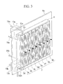
- FIG. 3 is a partial perspective view showing a portion of the structure of the thin-film production apparatus. As shown in FIG.
- the thin-film production apparatus 1 comprises a deposition chamber (the chamber) 6, a counter electrode 2, a heat spreader 5, a heat spreader holding mechanism 11, a discharge electrode 3, a deposition preventing plate 4, a support 7, a high-frequency power feeding transmission path 12, a matching unit 13, a high-vacuum evacuation unit 31, a low-vacuum evacuation unit 35, a base 37, and a control unit 100 that controls the entire apparatus.
- a deposition chamber the chamber 6
- the chamber the chamber 6
- a counter electrode 2 a heat spreader 5, a heat spreader holding mechanism 11, a discharge electrode 3, a deposition preventing plate 4, a support 7, a high-frequency power feeding transmission path 12, a matching unit 13, a high-vacuum evacuation unit 31, a low-vacuum evacuation unit 35, a base 37, and a control unit 100 that controls the entire apparatus.
- a deposition chamber the chamber 6
- a counter electrode 2 the thin-film production apparatus 1
- a heat spreader 5 the thin-film production apparatus 1
- the deposition chamber 6 is a vacuum container, and inside the container, an amorphous silicone i-layer or the like is deposited on a substrate 8.
- Inclining the substrate 8 slightly from the vertical is preferred as it suppresses any increase in the installation space required for the apparatus while enabling the substrate 8 to be supported with minimal effort by using the weight of the substrate 8 itself, and also improves the contact between the substrate 8 and the counter electrode 2, thereby improving the uniformity of the temperature distribution and the electrical potential distribution across the substrate 8.
- the counter electrode 2 is a conductive plate formed from a non-magnetic material that includes a holding device (not shown in the figure) that can hold the substrate 8. In those cases where self-cleaning is to be conducted, the use of a nickel alloy, aluminum or an aluminum alloy is preferred in terms of providing resistance to fluorine radicals.
- the counter electrode 2 is the opposing electrode to the discharge electrode 3 (for example, on the grounding side). One surface of the counter electrode 2 is positioned in close contact with the heat spreader 5, and during deposition, the other surface closely contacts the surface of the substrate 8.
- the temperature of the heat spreader 5 (the heating device) is controlled, either by circulating, within the inside of the heat spreader, a heating medium for which the temperature has been controlled, or by incorporating a temperature-controlled heater within the heat spreader, and therefore the heat spreader has a substantially uniform temperature across the heat spreader, and also performs the role of uniforming the temperature of the counter electrode 2 that contacts the heat spreader.
- the heating medium is a non-conductive medium, examples of which include highly thermally conductive gases such as hydrogen or helium, fluorine-based inert liquids, inert oils, and pure water. Of these, in terms of preventing the pressure from rising within a temperature range from 150°C to 250°C, and facilitating control, the use of a fluorine-based inert liquid (for example, a commercial product such as Galden or F05) is preferred.
- the heat spreader holding mechanism 11 holds the heat spreader 5 and the counter electrode 2 in a substantially parallel arrangement relative to the side surface of the deposition chamber 6 (the right side in FIG. 2 ). During deposition, the heat spreader 5, the counter electrode 2 and the substrate 8 are moved closer to the discharge electrode 3. This enables the distance d between the substrate 8 and the discharge electrode 3 to be set to approximately 7.5 mm or less, as described below.
- the discharge electrode 3 may be structured such that a series of rod-shaped longitudinal electrodes are combined in a substantially parallel arrangement, and the electrode may also be divided into a plurality of electrode units. In those cases where the discharge electrode 3 has a divided structure, the divisions are preferably formed to coincide with the number of feeding points.
- High-frequency electric power is supplied via the feeding points 53, 54 that connect the high-frequency power feeding transmission path 12a, 12b, thereby generating a plasma of the raw material gas between the discharge electrode 3 and the counter electrode 2, and generating a film on the substrate 8.
- the deposition preventing plate 4 is grounded, and restricts the region across which the plasma can expand, thereby restricting the deposition region.
- the support 7 holds the discharge electrode 3 in an insulated manner, so that the discharge electrode is aligned substantially parallel to the deposition preventing plate 4 and the side surface of the deposition chamber 6 (the left side in Fig. 2 ).
- the matching unit 13 matches the output-side impedance, and enables the high-frequency electric power to be transmitted from a high-frequency power source that is not shown in the figure, through a high-frequency power feeding transmission path 14 (14a and 14b) and the high-frequency power feeding transmission path 12, and into the discharge electrode 3.
- FIG. 3 is a partial perspective view showing a portion of the structure of the thin-film production apparatus 1.
- the discharge electrode 3 comprises, for example, 8 discharge electrodes 3a to 3h.
- Raw material gas is supplied to each of the discharge electrodes 3a to 3h from raw material gas pipes 16a and 16b that are connected near the feeding point 53 and the feeding point 54 respectively. This raw material gas is emitted substantially uniformly in the direction shown by the arrows in the figure (towards the counter electrode).
- electric power supply to the discharge electrodes 3a to 3h can also be conducted using more than 8, or fewer than 8 combinations of the matching units 13a and 13b, and the high-frequency power feeding transmission paths 14a and 14b.
- electric power may also be supplied from individual high-frequency power source units. In these cases, the number of groupings of the discharge electrodes 3a to 3h is preferably increased or decreased to match the number of the above combinations.
- FIG. 1 shows an enlarged view of the discharge electrode 3.
- the plurality of discharge electrodes 3 extend in a direction substantially parallel to the surface of the substrate 8 that is to undergo deposition (namely, in the depth direction from the paper surface), and are positioned in a substantially parallel arrangement relative to each other.
- a channel is formed in the surface of each discharge electrode 3 facing the surface of the aforementioned substrate 8, and the channel extends along the extending direction of the discharge electrode.
- the cross-sectional shape of each discharge electrode 3 in a direction perpendicular to the extending direction is a U-shape that is open on the surface of the electrode facing the substrate 8, comprising a base portion that is parallel to the substrate surface, and side portions 22a and 22b that extend towards the substrate 8 from either side of the base portion.
- a gas passage 21a through which the raw material gas flows is provided within the interior of the base portion, and an aforementioned heating medium passage 23 is provided within each of the two side portions 22a and 22b.
- the heating medium is supplied to the heating medium passage 23 using a heating medium supply device that is not shown in the figure, and temperature control is achieved by controlling the flow rate of the heating medium using the control unit 100.
- the heating medium can use the same types of media as the media described above for use within the heat spreader 5.
- the distance between the substrate 8 and the edges of the two side portions 22a and 22b of the discharge electrode 3 that are closest to the substrate is typically not less than 3 mm and not more than 10 mm, and is preferably not less than 4.5 mm and not more than 7.5 mm.
- the distance between the discharge electrode and the substrate has typically been within a range from approximately 20 mm to approximately 40 mm, but in this embodiment, the distance (gap) d between the substrate 8 and the edges of the two side portions 22a and 22b of the discharge electrode 3 that are closest to the substrate is a narrow gap.
- a film production method (vacuum treatment method) that uses a thin-film production apparatus with the above configuration is described below.
- the substrate 8 disposed inside the deposition chamber 6 under a reduced pressure atmosphere is heated using the heat spreader 5, and high-frequency electric power is supplied via the feeding points 53, 54 that connect the high-frequency power feeding transmission path 12a, 12b, thereby generating a plasma of the raw material gas between the discharge electrode 3 and the counter electrode 2, and depositing a film on the substrate 8.
- the quantity of the heating medium flowing through the heating medium passage 23 is controlled by the control unit 100, so that the difference between the temperature of the discharge electrode 3 and the temperature of the substrate is not more than 30°C, and is preferably approximately 20°C.
- the pressure within the deposition chamber 6 during the process is preferably set to a value of not less than 150 Pa and not more than 500 Pa.
- the degree of robustness improves, and the stability of the production apparatus also improves. Furthermore, if the temperature difference between the substrate 8 and the discharge electrode 3 is approximately 20°C, then the degree of robustness can be further improved.
- One reason for the improvement in film quality is thought to be due to the fact that the temperature difference between the substrate and the discharge electrode can be reduced by controlling the temperature of the discharge electrode, and the thermophoretic behavior of nanoclusters can be changed, thereby reducing the quantity of such nanoclusters incorporated into the film. Accordingly, under conditions where the substrate 8 and the discharge electrode 3 approach substantially the same temperature, meaning the temperature difference is small, an improvement in film quality is achieved.
- the thermal conductivity between the substrate 8 and the discharge electrode 3 improves, ensuring that the temperature difference does not widen.
- the SiH 2 /SiH ratio which correlates with the level of light-induced-degradation, can be suppressed to a low level, as shown in FIG. 5 , meaning the level of light-induced-degradation can be suppressed.
- the process becomes impractical. Accordingly, with the present invention, high-speed deposition can be conducted with no deterioration in performance. Furthermore, because the deposition pressure is set to a high level of not less than 150 Pa and not more than 500 Pa, the deposition rate increases and ion bombardment of the substrate 8 can be suppressed, thereby light-induced-degradation during high-speed deposition can also be suppressed. Because the deposition is conducted with a narrow gap, the plasma distribution tends to deteriorate at the deposition pressure lower than 150 Pa, whereas the plasma is prone to localization at the pressure exceeding 500 Pa, which is undesirable.
- the substrate temperature can be reduced, the band gap of the i-layer can be held at an appropriate level.
- the open-circuit voltage can be increased, and the performance of the produced solar cell can be improved.
- a thin-film production apparatus and a thin-film production method of the present embodiment stable film quality can be achieved even at a comparatively low substrate temperature of approximately 200°C, and consequently the deposition rate can be increased.
- the light-induced-degradation rate for the solar cell can also be reduced.
- the open-circuit voltage can be increased, leading to an improvement in the solar cell performance.
- a single-layer amorphous silicon solar cell was described as the solar cell, but the present invention is not limited to this example.
- the present invention can also be applied to other thin-film solar cells, including microcrystalline silicon solar cells, and multi-junction solar cells in which one or more amorphous silicon solar cell layers and microcrystalline solar cell layers are laminated together.
Landscapes
- Chemical & Material Sciences (AREA)
- Engineering & Computer Science (AREA)
- Materials Engineering (AREA)
- Plasma & Fusion (AREA)
- General Chemical & Material Sciences (AREA)
- Chemical Kinetics & Catalysis (AREA)
- Physics & Mathematics (AREA)
- Mechanical Engineering (AREA)
- Metallurgy (AREA)
- Organic Chemistry (AREA)
- Analytical Chemistry (AREA)
- Inorganic Chemistry (AREA)
- Photovoltaic Devices (AREA)
- Chemical Vapour Deposition (AREA)
Abstract
A vacuum treatment method and a vacuum treatment apparatus are provided in which the SiH2/SiH ratio does not increase even when the deposition rate is increased, thereby deterioration in the film quality is prevented and a high level of productivity can be achieved. A vacuum treatment method comprising the steps of heating a substrate (8) disposed inside a deposition chamber (6) under a reduced pressure atmosphere using a heat spreader (a heating device) (5), and supplying electric power to a discharge electrode (3) disposed in a position facing the substrate (8), thereby conducting a deposition on the substrate (8), wherein the deposition is conducted in a state where the temperature difference between the substrate (8) and the discharge electrode (3) is not more than 30°C. The deposition may also be conducted with the gap between the substrate (8) and the discharge electrode (3) set to not more than 7.5 mm.
Description
- The present invention relates to a vacuum treatment method and a vacuum treatment apparatus, and relates particularly to a vacuum treatment method and a vacuum treatment apparatus in which treatment of a substrate is conducted using a plasma.
- Plasma CVD devices are known examples of vacuum treatment apparatuses in which a semiconductor is gasified using a plasma, and a thin film of the semiconductor is then formed on a heated substrate. Solar cells in which a silicon-based thin film deposited on the surface of a glass substrate comprises laminated p-layer, i-layer and n-layer, and light irradiated onto the i-layer is converted to electrical power are also known.
Patent Citation 1: Japanese Unexamined Patent Application, Publication No.Hei 6-283435
Patent Citation 2: Japanese Unexamined Patent Application, Publication No.Hei 7-230960 - In recent years, demands have grown for reductions in the production costs of solar cells. As a result, a deposition rate within the aforementioned vacuum treatment apparatus for the i-layer that functions as a photovoltaic layer must be increased. However, if this deposition rate is increased, then a SiH2/SiH ratio, which indicates the state of silicon-hydrogen bonding within an amorphous silicon film, also increases. The SiH2/SiH ratio is used as an indicator of film quality. An increase in the SiH2/SiH ratio indicates a reduction in the quantity of Si-Si bonds and an increase in the number of defects after light soaking, meaning a deterioration in the film quality.
- It is known that raising the substrate temperature can be used to suppress the increase in the SiH2/SiH ratio that occurs when the deposition rate is increased. This reduces the SiH2/SiH ratio and improves the film quality. However, in the case of deposition of the i-layer of the amorphous silicon solar cell, problems arise in that considerable time is needed for the substrate temperature to stabilize because the quantity of heat flowing in and out of the substrate increases as the deposition temperature (the substrate temperature) is raised, and in that fluctuations in the temperature may cause a deterioration in the performance of the solar cell. Furthermore, if the substrate temperature is raised, then the band gap for the i-layer may deviate from the appropriate range, and the boron that acts as the dopant within the underlying p-layer may diffuse, causing a reduction in the open-circuit voltage and deterioration in the performance of the cell.
Accordingly, improving the film quality and improving the deposition rate exist in a trade-off relationship, and achieving improvements in both the film quality and the deposition rate would be highly desirable. - The present invention has an object of providing a vacuum treatment method and a vacuum treatment apparatus, in which the SiH2/SiH ratio does not increase even when the deposition rate is increased, and in which deterioration in the film quality is prevented and a high level of productivity can be achieved.
- A vacuum treatment method of the present invention is a method comprising the steps of heating a substrate disposed inside a deposition chamber under a reduced pressure atmosphere using a heating device, supplying a raw material gas to the deposition chamber, and supplying electric power to a discharge electrode disposed in a position facing the substrate, thereby conducting a deposition on the substrate, wherein the deposition is conducted in a state in which the temperature difference between the substrate and the discharge electrode is not more than 30°C.
- In the vacuum treatment method of the present invention, because the temperature difference between the substrate and the discharge electrode is small, the quantity of heat flowing in and out of the substrate is reduced, and fluctuations in the substrate temperature during the production process for a photovoltaic device (such as a solar cell) are also reduced. Therefore, the process window for selection of the deposition conditions is broad, thus enabling the conditions to be set within reliable ranges. As a result, restrictions on the deposition conditions can be relaxed, and performance stability improves. In a particularly preferred configuration, if the aforementioned temperature difference between the substrate and the discharge electrode is reduced to approximately 20°C, then the degree of robustness can be further improved.
- In the vacuum treatment method of the present invention, deposition is preferably conducted with the gap between the substrate and the discharge electrode set to a value of not less than 4.5 mm and not more than 7.5 mm.
- This improves the thermal conductivity between the substrate and the discharge electrode, and therefore ensures that the temperature difference between the substrate and the discharge electrode does not widen. As a result, even if the substrate temperature during high-speed deposition is set to a comparatively low temperature of 200°C or lower, the SiH2/SiH ratio, which correlates with the level of light-induced-degradation, can be suppressed to a low level, enabling an improvement in the quality of the produced film.
- A vacuum treatment apparatus of the present invention is a apparatus comprising a chamber that forms a deposition chamber under a reduced pressure atmosphere, a heating device for heating a substrate disposed inside the chamber, a supply device for supplying a raw material gas into the deposition chamber, a discharge electrode that is disposed in a position facing the substrate, and a heating medium passage for regulating a temperature of the discharge electrode, in which deposition on the substrate is conducted by supplying electric power to the discharge electrode, wherein the vacuum treatment apparatus further comprises mechanisms for regulating a temperature difference between the substrate and the discharge electrode, and a deposition pressure.
- With the vacuum treatment apparatus of the present invention, in those environments where the discharge electrode is prone to temperature increases as a result of the plasma generation at the discharge electrode during deposition, the temperature of the discharge electrode can be regulated. As the result, the temperature difference between the substrate and the discharge electrode can be set to a value that is suitable for deposition, thereby enabling the deposition pressure to be set to a level that provides a stable plasma. For example, if a control unit is provided that controls the deposition such that the temperature difference between the substrate and the discharge electrode is not more than 30°C, and the vacuum treatment is then conducted under the control of this control unit, then if the gap between the substrate and the discharge electrode is set to a value of not less than 4.5 mm and not more than 7.5 mm, and the deposition pressure is set to a value of not less than 150 Pa and not more than 500 Pa, the effects of temperature fluctuation during the production process for a photovoltaic device are minimal, and the plasma adopts a stable state, thereby restrictions on the deposition conditions can be relaxed, enabling an improvement in the performance stability. Furthermore, by setting the deposition pressure to a relatively high value, the deposition rate can be increased, which is particularly desirable.
- In the vacuum treatment apparatus of the present invention, the heating medium passage may be provided inside the discharge electrode.
- The discharge electrode may be a plurality of substantially parallel electrodes that extend in a substantially parallel arrangement relative to the surface of the substrate on which deposition is to be conducted. A channel may be formed in each discharge electrode, in the surface that faces the substrate surface, with this channel extending along the lengthwise direction of the discharge electrode. In other words, the cross-sectional shape of each discharge electrode, in a direction perpendicular to the lengthwise direction, is a U-shape that is open on the substrate-side of the electrode, comprising a base portion that is parallel to the substrate surface, and side portions that extend towards the substrate from either side of the base portion. A raw material gas passage may be provided within the interior of the base portion, and the raw material gas is emitted substantially uniformly from a multitude of small apertures provided within the base portion of the U-shape, thereby lengthening the distance in which the raw material gas travels before reaching the substrate, and enabling uniform supply of the raw material gas. The aforementioned heating medium passage can be provided inside the two side portions of each of the discharge electrodes. In other words, the discharge electrode acts as a holder for holding the heating medium passage. Because this improves the thermal conductivity between the discharge electrode and the heating medium, control of the discharge electrode temperature is excellent. Furthermore, in order to ensure a more uniform flow rate distribution for the raw material gas, a perforated plate may be provided on the substrate-side raw material emission portion within the open portion of the base portion of each of the discharge electrodes with a U-shaped cross-section.
- In the vacuum treatment apparatus of the present invention, the discharge electrode is preferably positioned so that the gap between the discharge electrode and the substrate is not less than 4.5 mm and not more than 7.5 mm.
- This improves the thermal conductivity between the substrate and the discharge electrode, prevents the temperature difference from widening. As a result, the degradation rate can be suppressed even at comparatively low substrate temperature and the deposition quality to be improved, even if the deposition rate is raised.
- According to the present invention, because the film quality is stable even at comparatively low temperatures, the deposition rate can be increased while the light-induced-degradation rate of the layers of the photovoltaic device is reduced, thereby a high level of productivity can be obtained. Moreover, because the deposition temperature need be raised no higher than necessary, an improvement in the performance of the photovoltaic device arising from an increase in the open-circuit voltage can also be achieved.
-
- [
FIG. 1 ] An enlarged view showing a discharge electrode used in a thin-film production apparatus according to an embodiment of the present invention. - [
FIG. 2 ] A schematic illustration showing the structure of a thin-film production apparatus according to the present invention, viewed from the side of the thin-film production apparatus. - [
FIG. 3 ] A partial perspective view showing a portion of the structure of the same thin-film production apparatus. - [
FIG. 4 ] A graph showing the temperature dependency of the light-induced-degradation rate of a film. - [
FIG. 5 ] A diagram showing that, for low-temperature deposition at a substrate temperature of not more than 200°C, when the temperature difference between the substrate and the discharge electrode is not more than 30°C, the film quality can be maintained, and the film degradation rate is independent of the temperature. - [
FIG. 6 ] A graph showing the relationship between the temperature difference between the substrate and the discharge electrode, and the SiH2/SiH ratio. - [
FIG. 7 ] A graph showing the relationship between the gap distance and the SiH2/SiH ratio under a variety of conditions. -
- 1: Thin-film production apparatus
- 2: Counter electrode
- 3: Discharge electrode
- 3a: Discharge electrode
- 5: Heat spreader (heating device)
- 8: Substrate
- 22a, 22b: Side portion
- 23: Heating medium passage
- 100: Control unit
- An embodiment of a thin-film production apparatus (a vacuum treatment apparatus) that is capable of conducting high-speed deposition is described below.
FIG. 1 is a diagram showing a discharge electrode used in the thin-film production apparatus according to this embodiment, andFIG. 2 is a schematic illustration showing the structure of the thin-film production apparatus, viewed from the side of the thin-film production apparatus 1.FIG. 3 is a partial perspective view showing a portion of the structure of the thin-film production apparatus.
As shown inFIG. 2 , the thin-film production apparatus 1 comprises a deposition chamber (the chamber) 6, acounter electrode 2, aheat spreader 5, a heatspreader holding mechanism 11, adischarge electrode 3, adeposition preventing plate 4, a support 7, a high-frequency power feeding transmission path 12, a matching unit 13, a high-vacuum evacuation unit 31, a low-vacuum evacuation unit 35, abase 37, and acontrol unit 100 that controls the entire apparatus. In the figure, structures relating to the gas supply are omitted. The thin-film production apparatus 1 is used, for example, for producing solar cells such as single-layer amorphous silicon solar cells. - The
deposition chamber 6 is a vacuum container, and inside the container, an amorphous silicone i-layer or the like is deposited on asubstrate 8. Thedeposition chamber 6 is supported on top of the base 37 with an inclination from the z direction (the vertical direction) of θ = 7° to 12°. As a result, the deposition treatment surface of thesubstrate 8 on thecounter electrode 2 is tilted upwards by 7° to 12° relative to the z direction. Inclining thesubstrate 8 slightly from the vertical is preferred as it suppresses any increase in the installation space required for the apparatus while enabling thesubstrate 8 to be supported with minimal effort by using the weight of thesubstrate 8 itself, and also improves the contact between thesubstrate 8 and thecounter electrode 2, thereby improving the uniformity of the temperature distribution and the electrical potential distribution across thesubstrate 8. - The
counter electrode 2 is a conductive plate formed from a non-magnetic material that includes a holding device (not shown in the figure) that can hold thesubstrate 8. In those cases where self-cleaning is to be conducted, the use of a nickel alloy, aluminum or an aluminum alloy is preferred in terms of providing resistance to fluorine radicals. Thecounter electrode 2 is the opposing electrode to the discharge electrode 3 (for example, on the grounding side). One surface of thecounter electrode 2 is positioned in close contact with theheat spreader 5, and during deposition, the other surface closely contacts the surface of thesubstrate 8. The temperature of the heat spreader 5 (the heating device) is controlled, either by circulating, within the inside of the heat spreader, a heating medium for which the temperature has been controlled, or by incorporating a temperature-controlled heater within the heat spreader, and therefore the heat spreader has a substantially uniform temperature across the heat spreader, and also performs the role of uniforming the temperature of thecounter electrode 2 that contacts the heat spreader. - The heating medium is a non-conductive medium, examples of which include highly thermally conductive gases such as hydrogen or helium, fluorine-based inert liquids, inert oils, and pure water. Of these, in terms of preventing the pressure from rising within a temperature range from 150°C to 250°C, and facilitating control, the use of a fluorine-based inert liquid (for example, a commercial product such as Galden or F05) is preferred.
The heatspreader holding mechanism 11 holds theheat spreader 5 and thecounter electrode 2 in a substantially parallel arrangement relative to the side surface of the deposition chamber 6 (the right side inFIG. 2 ). During deposition, theheat spreader 5, thecounter electrode 2 and thesubstrate 8 are moved closer to thedischarge electrode 3. This enables the distance d between thesubstrate 8 and thedischarge electrode 3 to be set to approximately 7.5 mm or less, as described below. - The
discharge electrode 3 may be structured such that a series of rod-shaped longitudinal electrodes are combined in a substantially parallel arrangement, and the electrode may also be divided into a plurality of electrode units. In those cases where thedischarge electrode 3 has a divided structure, the divisions are preferably formed to coincide with the number of feeding points. High-frequency electric power is supplied via the feeding points 53, 54 that connect the high-frequency powerfeeding transmission path discharge electrode 3 and thecounter electrode 2, and generating a film on thesubstrate 8. Thedeposition preventing plate 4 is grounded, and restricts the region across which the plasma can expand, thereby restricting the deposition region. The support 7 holds thedischarge electrode 3 in an insulated manner, so that the discharge electrode is aligned substantially parallel to thedeposition preventing plate 4 and the side surface of the deposition chamber 6 (the left side inFig. 2 ). - The matching unit 13 (13a and 13b) matches the output-side impedance, and enables the high-frequency electric power to be transmitted from a high-frequency power source that is not shown in the figure, through a high-frequency power feeding transmission path 14 (14a and 14b) and the high-frequency power feeding transmission path 12, and into the
discharge electrode 3. -
FIG. 3 is a partial perspective view showing a portion of the structure of the thin-film production apparatus 1. In this embodiment, thedischarge electrode 3 comprises, for example, 8discharge electrodes 3a to 3h.
Raw material gas is supplied to each of thedischarge electrodes 3a to 3h from rawmaterial gas pipes feeding point 53 and thefeeding point 54 respectively. This raw material gas is emitted substantially uniformly in the direction shown by the arrows in the figure (towards the counter electrode).
However, electric power supply to thedischarge electrodes 3a to 3h can also be conducted using more than 8, or fewer than 8 combinations of thematching units feeding transmission paths discharge electrodes 3a to 3h is preferably increased or decreased to match the number of the above combinations. -
FIG. 1 shows an enlarged view of thedischarge electrode 3. The plurality ofdischarge electrodes 3 extend in a direction substantially parallel to the surface of thesubstrate 8 that is to undergo deposition (namely, in the depth direction from the paper surface), and are positioned in a substantially parallel arrangement relative to each other. A channel is formed in the surface of eachdischarge electrode 3 facing the surface of theaforementioned substrate 8, and the channel extends along the extending direction of the discharge electrode. In other words, the cross-sectional shape of eachdischarge electrode 3 in a direction perpendicular to the extending direction is a U-shape that is open on the surface of the electrode facing thesubstrate 8, comprising a base portion that is parallel to the substrate surface, andside portions substrate 8 from either side of the base portion. Agas passage 21a through which the raw material gas flows is provided within the interior of the base portion, and an aforementionedheating medium passage 23 is provided within each of the twoside portions heating medium passage 23 using a heating medium supply device that is not shown in the figure, and temperature control is achieved by controlling the flow rate of the heating medium using thecontrol unit 100. The heating medium can use the same types of media as the media described above for use within theheat spreader 5. - The distance between the
substrate 8 and the edges of the twoside portions discharge electrode 3 that are closest to the substrate is typically not less than 3 mm and not more than 10 mm, and is preferably not less than 4.5 mm and not more than 7.5 mm. In conventional apparatus, the distance between the discharge electrode and the substrate has typically been within a range from approximately 20 mm to approximately 40 mm, but in this embodiment, the distance (gap) d between thesubstrate 8 and the edges of the twoside portions discharge electrode 3 that are closest to the substrate is a narrow gap. - A film production method (vacuum treatment method) that uses a thin-film production apparatus with the above configuration is described below.
Thesubstrate 8 disposed inside thedeposition chamber 6 under a reduced pressure atmosphere is heated using theheat spreader 5, and high-frequency electric power is supplied via the feeding points 53, 54 that connect the high-frequency powerfeeding transmission path discharge electrode 3 and thecounter electrode 2, and depositing a film on thesubstrate 8. - During this process, the quantity of the heating medium flowing through the
heating medium passage 23 is controlled by thecontrol unit 100, so that the difference between the temperature of thedischarge electrode 3 and the temperature of the substrate is not more than 30°C, and is preferably approximately 20°C. Furthermore, the pressure within thedeposition chamber 6 during the process is preferably set to a value of not less than 150 Pa and not more than 500 Pa. - In conventional thin-film production apparatus, temperature control using a heating medium is not conducted, and the temperature dependency of the light-induced-degradation rate of the film is strong, as shown in
FIG. 4 . As a result, if the temperature of thesubstrate 8 is increased in order to increase the deposition rate, the degree of temperature fluctuation increases, causing a deterioration in the stability of the film quality.
In this embodiment, by restricting the temperature difference between thesubstrate 8 and thedischarge electrode 3 to not more than 30°C, substrate temperature dependency is less likely to appear, as shown inFIG. 6 . As a result, the process window broadens, therefore selecting conditions that optimize the deposition conditions is easier, and the film quality also improves. In other words, in the conventional technology, when the temperature of thesubstrate 8 is maintained at a high level, the quantity of heat flowing in and out of thesubstrate 8 is large, resulting in a deterioration of the film quality due to temperature fluctuations, whereas in the embodiment of the present invention, the degree of robustness improves, and the stability of the production apparatus also improves. Furthermore, if the temperature difference between thesubstrate 8 and thedischarge electrode 3 is approximately 20°C, then the degree of robustness can be further improved.
One reason for the improvement in film quality is thought to be due to the fact that the temperature difference between the substrate and the discharge electrode can be reduced by controlling the temperature of the discharge electrode, and the thermophoretic behavior of nanoclusters can be changed, thereby reducing the quantity of such nanoclusters incorporated into the film. Accordingly, under conditions where thesubstrate 8 and thedischarge electrode 3 approach substantially the same temperature, meaning the temperature difference is small, an improvement in film quality is achieved. - By setting the distance between the
discharge electrode 3 and thesubstrate 8 to a value not less than 4.5 mm and not more than 7.5 mm, the thermal conductivity between thesubstrate 8 and thedischarge electrode 3 improves, ensuring that the temperature difference does not widen. As a result, during high-speed deposition, and even if the substrate temperature is set to a comparatively low temperature of 200°C or lower, the SiH2/SiH ratio, which correlates with the level of light-induced-degradation, can be suppressed to a low level, as shown inFIG. 5 , meaning the level of light-induced-degradation can be suppressed. This observation is thought to be due to the fact that the gas replacement rate near the surface of thesubstrate 8 can be improved by narrowing the gap, thereby reducing the quantity of clusters in the discharge region and reducing the incorporation of such clusters into the film. As shown inFIG. 7 , the conventional tendency for the SiH2/SiH ratio to increase together with increases in the deposition rate is moderated, and it is evident that the SiH2/SiH ratio decreases as the gap distance is narrowed, and that favorable results can be obtained within the range from not less than 4.5 mm to not more than 10 mm, particularly at gap distances of not more than 7.5 mm,. At gaps of 3 mm or less, because small deformations in the substrate or the discharge electrode can affect the properties of the deposited film, the process becomes impractical. Accordingly, with the present invention, high-speed deposition can be conducted with no deterioration in performance. Furthermore, because the deposition pressure is set to a high level of not less than 150 Pa and not more than 500 Pa, the deposition rate increases and ion bombardment of thesubstrate 8 can be suppressed, thereby light-induced-degradation during high-speed deposition can also be suppressed. Because the deposition is conducted with a narrow gap, the plasma distribution tends to deteriorate at the deposition pressure lower than 150 Pa, whereas the plasma is prone to localization at the pressure exceeding 500 Pa, which is undesirable. - Furthermore, mainly in the deposition of an i-layer of an amorphous silicon solar cell, because the substrate temperature can be reduced, the band gap of the i-layer can be held at an appropriate level. As a result, the open-circuit voltage can be increased, and the performance of the produced solar cell can be improved.
- As described above, according to a thin-film production apparatus and a thin-film production method of the present embodiment, stable film quality can be achieved even at a comparatively low substrate temperature of approximately 200°C, and consequently the deposition rate can be increased. The light-induced-degradation rate for the solar cell can also be reduced. Moreover, because the i-layer is not deposited at high temperature, the open-circuit voltage can be increased, leading to an improvement in the solar cell performance.
- In the embodiment described above, a single-layer amorphous silicon solar cell was described as the solar cell, but the present invention is not limited to this example. For example, the present invention can also be applied to other thin-film solar cells, including microcrystalline silicon solar cells, and multi-junction solar cells in which one or more amorphous silicon solar cell layers and microcrystalline solar cell layers are laminated together.
Claims (6)
- A vacuum treatment method comprising the steps of heating a substrate disposed inside a deposition chamber under a reduced pressure atmosphere using a heating device, supplying a raw material gas to the deposition chamber, and supplying electric power to a discharge electrode disposed in a position facing the substrate, thereby conducting a deposition on the substrate, wherein
the deposition is conducted in a state in which a temperature difference between the substrate and the discharge electrode is not more than 30°C. - The vacuum treatment method according to claim 1, wherein the deposition is conducted with a gap between the substrate and the discharge electrode set to a value of not less than 4.5 mm and not more than 7.5 mm.
- The vacuum treatment method according to claim 2, wherein the deposition is conducted with a deposition pressure inside the deposition chamber set to a value of not less than 150 Pa and not more than 500 Pa.
- A vacuum treatment apparatus comprising a chamber that forms a deposition chamber under a reduced pressure atmosphere, a heating device for heating a substrate disposed inside the chamber, a supply device for supplying a raw material gas into the deposition chamber, a discharge electrode that is disposed in a position facing the substrate, and a heating medium passage for regulating a temperature of the discharge electrode, in which deposition on the substrate is conducted by supplying electric power to the discharge electrode, wherein
the vacuum treatment apparatus further comprises mechanisms for regulating a temperature difference between the substrate and the discharge electrode, and a deposition pressure. - The vacuum treatment apparatus according to claim 4, wherein the heating medium passage is provided inside the discharge electrode.
- The vacuum treatment apparatus according to claim 5, wherein the discharge electrode is positioned so that a distance between the discharge electrode and the substrate is not less than 4.5 mm and not more than 7.5 mm.
Applications Claiming Priority (2)
| Application Number | Priority Date | Filing Date | Title |
|---|---|---|---|
| JP2007043270A JP4795990B6 (en) | 2007-02-23 | Vacuum processing method and vacuum processing apparatus | |
| PCT/JP2008/051445 WO2008102622A1 (en) | 2007-02-23 | 2008-01-30 | Vacuum processing method and vacuum processing apparatus |
Publications (2)
| Publication Number | Publication Date |
|---|---|
| EP2113936A1 true EP2113936A1 (en) | 2009-11-04 |
| EP2113936A4 EP2113936A4 (en) | 2010-11-17 |
Family
ID=39709901
Family Applications (1)
| Application Number | Title | Priority Date | Filing Date |
|---|---|---|---|
| EP08704208A Withdrawn EP2113936A4 (en) | 2007-02-23 | 2008-01-30 | VACUUM PROCESSING METHOD AND VACUUM PROCESSING APPARATUS |
Country Status (5)
| Country | Link |
|---|---|
| US (1) | US8263193B2 (en) |
| EP (1) | EP2113936A4 (en) |
| CN (1) | CN101548365B (en) |
| AU (1) | AU2008218436A1 (en) |
| WO (1) | WO2008102622A1 (en) |
Family Cites Families (14)
| Publication number | Priority date | Publication date | Assignee | Title |
|---|---|---|---|---|
| JPH06283435A (en) | 1993-03-26 | 1994-10-07 | Sanyo Electric Co Ltd | Method of forming amorphous silicon film by plasma cvd |
| JP3146112B2 (en) | 1993-12-24 | 2001-03-12 | シャープ株式会社 | Plasma CVD equipment |
| JPH0799744B2 (en) | 1993-12-27 | 1995-10-25 | アプライド マテリアルズ インコーポレイテッド | Thin film formation method |
| JPH07254590A (en) | 1994-03-15 | 1995-10-03 | Fujitsu Ltd | Method for manufacturing semiconductor device |
| JPH09148322A (en) | 1995-11-22 | 1997-06-06 | Sharp Corp | Silicon oxide film forming method and plasma CVD film forming apparatus |
| US6217662B1 (en) * | 1997-03-24 | 2001-04-17 | Cree, Inc. | Susceptor designs for silicon carbide thin films |
| JP3447647B2 (en) * | 2000-02-25 | 2003-09-16 | 株式会社日立製作所 | Sample etching method |
| US6776875B2 (en) * | 2000-02-28 | 2004-08-17 | Applied Materials Inc. | Semiconductor substrate support assembly having lobed o-rings therein |
| TWI276366B (en) * | 2002-07-09 | 2007-03-11 | Semiconductor Energy Lab | Production apparatus and method of producing a light-emitting device by using the same apparatus |
| JP2004266111A (en) * | 2003-03-03 | 2004-09-24 | Fuji Electric Holdings Co Ltd | Method for manufacturing microcrystalline film and microcrystalline thin film solar cell |
| US20050067934A1 (en) * | 2003-09-26 | 2005-03-31 | Ishikawajima-Harima Heavy Industries Co., Ltd. | Discharge apparatus, plasma processing method and solar cell |
| JP4519695B2 (en) * | 2005-03-29 | 2010-08-04 | 三菱重工業株式会社 | Thin film manufacturing apparatus and thin film manufacturing method |
| US20060269690A1 (en) * | 2005-05-27 | 2006-11-30 | Asm Japan K.K. | Formation technology for nanoparticle films having low dielectric constant |
| JP4625397B2 (en) | 2005-10-18 | 2011-02-02 | 三菱重工業株式会社 | Discharge electrode, thin film manufacturing apparatus and solar cell manufacturing method |
-
2008
- 2008-01-30 AU AU2008218436A patent/AU2008218436A1/en not_active Abandoned
- 2008-01-30 EP EP08704208A patent/EP2113936A4/en not_active Withdrawn
- 2008-01-30 US US12/311,184 patent/US8263193B2/en not_active Expired - Fee Related
- 2008-01-30 WO PCT/JP2008/051445 patent/WO2008102622A1/en not_active Ceased
- 2008-01-30 CN CN2008800008504A patent/CN101548365B/en not_active Expired - Fee Related
Also Published As
| Publication number | Publication date |
|---|---|
| WO2008102622A1 (en) | 2008-08-28 |
| US8263193B2 (en) | 2012-09-11 |
| CN101548365B (en) | 2011-01-26 |
| JP4795990B2 (en) | 2011-10-19 |
| EP2113936A4 (en) | 2010-11-17 |
| JP2008210826A (en) | 2008-09-11 |
| CN101548365A (en) | 2009-09-30 |
| US20100068411A1 (en) | 2010-03-18 |
| AU2008218436A1 (en) | 2008-08-28 |
Similar Documents
| Publication | Publication Date | Title |
|---|---|---|
| US8586484B2 (en) | Film forming method and film forming apparatus | |
| US6427622B2 (en) | Hot wire chemical vapor deposition method and apparatus using graphite hot rods | |
| EP0648373B1 (en) | Microwave energized deposition process with substrate temperature control | |
| US6214706B1 (en) | Hot wire chemical vapor deposition method and apparatus using graphite hot rods | |
| US20100144122A1 (en) | Hybrid chemical vapor deposition process combining hot-wire cvd and plasma-enhanced cvd | |
| KR20090031492A (en) | Method and apparatus for depositing microcrystalline silicon film for optoelectronic devices | |
| US20110308735A1 (en) | Vacuum processing apparatus | |
| JPWO2010013746A1 (en) | Deposited film forming apparatus and deposited film forming method | |
| US20110220026A1 (en) | Plasma processing device | |
| US6531654B2 (en) | Semiconductor thin-film formation process, and amorphous silicon solar-cell device | |
| JP4936297B2 (en) | Plasma processing apparatus, plasma processing method, and semiconductor device | |
| KR101708397B1 (en) | Method and apparatus for forming a dielectric layer on a substrate | |
| US8263193B2 (en) | Vacuum treatment method | |
| JP5772941B2 (en) | Plasma CVD equipment | |
| US20090130337A1 (en) | Programmed high speed deposition of amorphous, nanocrystalline, microcrystalline, or polycrystalline materials having low intrinsic defect density | |
| JP2007115757A (en) | Discharge electrode, thin film manufacturing apparatus, and manufacturing method of solar cell | |
| WO2010082120A1 (en) | Amorphous carbon, method of manufacturing the same, and solar cell including the same | |
| EP0619918A1 (en) | Microwave energized deposition process using a pressure lower than the minimum point pressure of the paschen curve | |
| US20090050058A1 (en) | Programmed high speed deposition of amorphous, nanocrystalline, microcrystalline, or polycrystalline materials having low intrinsic defect density | |
| US11502217B1 (en) | Methods and apparatus for reducing as-deposited and metastable defects in Amorphousilicon | |
| JP4795990B6 (en) | Vacuum processing method and vacuum processing apparatus | |
| JP2007266094A (en) | Plasma cvd device and method for forming semiconductor thin-film by same | |
| JP5053595B2 (en) | DLC film forming method and DLC film manufacturing apparatus | |
| JP2018046302A (en) | Plasma cvd system and plasma cvd method | |
| JP2011151105A (en) | Plasma cvd apparatus |
Legal Events
| Date | Code | Title | Description |
|---|---|---|---|
| PUAI | Public reference made under article 153(3) epc to a published international application that has entered the european phase |
Free format text: ORIGINAL CODE: 0009012 |
|
| 17P | Request for examination filed |
Effective date: 20090325 |
|
| AK | Designated contracting states |
Kind code of ref document: A1 Designated state(s): AT BE BG CH CY CZ DE DK EE ES FI FR GB GR HR HU IE IS IT LI LT LU LV MC MT NL NO PL PT RO SE SI SK TR |
|
| DAX | Request for extension of the european patent (deleted) | ||
| A4 | Supplementary search report drawn up and despatched |
Effective date: 20101020 |
|
| 17Q | First examination report despatched |
Effective date: 20130221 |
|
| STAA | Information on the status of an ep patent application or granted ep patent |
Free format text: STATUS: THE APPLICATION IS DEEMED TO BE WITHDRAWN |
|
| 18D | Application deemed to be withdrawn |
Effective date: 20140801 |