EP2113779A1 - Testable integrated circuit and integrated circuit test method - Google Patents
Testable integrated circuit and integrated circuit test method Download PDFInfo
- Publication number
- EP2113779A1 EP2113779A1 EP08290418A EP08290418A EP2113779A1 EP 2113779 A1 EP2113779 A1 EP 2113779A1 EP 08290418 A EP08290418 A EP 08290418A EP 08290418 A EP08290418 A EP 08290418A EP 2113779 A1 EP2113779 A1 EP 2113779A1
- Authority
- EP
- European Patent Office
- Prior art keywords
- shift register
- test
- integrated circuit
- instruction
- register
- Prior art date
- Legal status (The legal status is an assumption and is not a legal conclusion. Google has not performed a legal analysis and makes no representation as to the accuracy of the status listed.)
- Ceased
Links
- 238000010998 test method Methods 0.000 title claims abstract description 6
- 238000012360 testing method Methods 0.000 claims abstract description 105
- 238000000034 method Methods 0.000 claims description 21
- 230000008878 coupling Effects 0.000 claims description 3
- 238000010168 coupling process Methods 0.000 claims description 3
- 238000005859 coupling reaction Methods 0.000 claims description 3
- 239000000523 sample Substances 0.000 description 4
- 238000013459 approach Methods 0.000 description 2
- 230000002457 bidirectional effect Effects 0.000 description 2
- 239000000872 buffer Substances 0.000 description 2
- 238000013461 design Methods 0.000 description 2
- 238000011960 computer-aided design Methods 0.000 description 1
- 230000001419 dependent effect Effects 0.000 description 1
- 238000005259 measurement Methods 0.000 description 1
- 239000003607 modifier Substances 0.000 description 1
- 230000006641 stabilisation Effects 0.000 description 1
- 238000011105 stabilization Methods 0.000 description 1
Images


Classifications
-
- G—PHYSICS
- G01—MEASURING; TESTING
- G01R—MEASURING ELECTRIC VARIABLES; MEASURING MAGNETIC VARIABLES
- G01R31/00—Arrangements for testing electric properties; Arrangements for locating electric faults; Arrangements for electrical testing characterised by what is being tested not provided for elsewhere
- G01R31/28—Testing of electronic circuits, e.g. by signal tracer
- G01R31/317—Testing of digital circuits
- G01R31/3181—Functional testing
- G01R31/3185—Reconfiguring for testing, e.g. LSSD, partitioning
- G01R31/318533—Reconfiguring for testing, e.g. LSSD, partitioning using scanning techniques, e.g. LSSD, Boundary Scan, JTAG
- G01R31/318544—Scanning methods, algorithms and patterns
- G01R31/31855—Interconnection testing, e.g. crosstalk, shortcircuits
-
- G—PHYSICS
- G01—MEASURING; TESTING
- G01R—MEASURING ELECTRIC VARIABLES; MEASURING MAGNETIC VARIABLES
- G01R31/00—Arrangements for testing electric properties; Arrangements for locating electric faults; Arrangements for electrical testing characterised by what is being tested not provided for elsewhere
- G01R31/28—Testing of electronic circuits, e.g. by signal tracer
- G01R31/317—Testing of digital circuits
- G01R31/3181—Functional testing
- G01R31/3185—Reconfiguring for testing, e.g. LSSD, partitioning
- G01R31/318533—Reconfiguring for testing, e.g. LSSD, partitioning using scanning techniques, e.g. LSSD, Boundary Scan, JTAG
- G01R31/318572—Input/Output interfaces
Definitions
- the present invention relates to an integrated circuit (IC) comprising a plurality of interconnections and a test arrangement comprising a test access port and a shift register comprising a plurality of cells, each coupled to a respective interconnection via at least one signal driver.
- IC integrated circuit
- the present invention further relates to a method for testing such an IC.
- an IC Before releasing an IC into the market, an IC must be tested to ensure that the IC does not produce any errors to avoid customer returns and occurrence of potentially dangerous situations caused by unexpected IC behavior, e.g. in application domains where the IC plays an integral part in controlling a device, e.g. a car or another vehicle.
- a hard error is an error caused by a physical fault such as an open, short or bridging fault.
- a soft error may be caused by a deviation from an intended IC design parameter, and may only occur when the IC is brought into certain modes of operation, e.g. a high-frequency operational mode. Such errors are usually more difficult to detect.
- An example of such an error is the failure of an external interconnection of an IC to communicate the intended signal behavior at high frequencies. Such failures may occur when an IC interconnect, e.g. a bond pad or a pin, does not exhibit the intended signal response characteristics. Such characteristics can be defined in terms of response parameters to voltage and current stimuli.
- a well-established test approach for testing IC interconnections is the IEEE 1149.1 standard, which is more commonly known as boundary scan test (BST).
- BST boundary scan test
- an IC is extended with a test arrangement including a boundary scan register which is located between the IC interconnections and the internals of the IC. In functional mode, this register is transparent such that the shift register cells do not influence the signals communicated between the IC internals and the interconnects.
- the boundary scan register is used to communicate, i.e. provide or capture, test stimuli with the interconnects to test for the presence of interconnect faults.
- This test method is well-suited to detect hard errors in the interconnections, but is less suited to detect different types of parametric errors because the signal drivers that couple the shift register cells to the interconnects are kept in mode as defined in the IEEE 1149.1 standard.
- the present invention seeks to provide an IC for which the interconnect DC parameters can be determined using less dedicated hardware.
- the drivers between the interconnections and the cells of the shift register can be brought into any desired state, which facilitates the automated testing of different DC parameters of the interconnections using the driver appropriate configuration data and test stimuli for the interconnections.
- At least some of the cells of the further shift register may be coupled to the control terminal of more than one driver to facilitate testing blocks of drivers in the same DC mode, thus reducing the amount of shift register cells required.
- the test access port further comprises an instruction register and decoding logic coupled to the instruction register for connecting the shift register to a test data input in response to the presence of a first dedicated instruction in the instruction register, and for connecting the further shift register to the test data input in response to the presence of a further dedicated instruction in the instruction register.
- a method of testing an integrated circuit comprising connecting an external tester to the interconnections; loading a first test pattern into the shift register; loading a further test pattern into the further shift register; and determining respective parameter values of the interconnections.
- the method may further comprise providing the interconnections with respective stimuli from the external tester, and wherein the step of determining respective parameter values of the interconnections comprises capturing said values in respective cells of the shift register. This facilitates shifting out the test results via the test data output of the test access port.
- the TAP 170 which may be a boundary scan test compliant TAP, further comprises an instruction register 150 coupled to decoding logic 155.
- the decoding logic 155 is responsible for decoding instructions that are shifted into the instruction register 150 e.g. during the SHIFT-IR mode of the state machine of the TAP controller (not shown), which are decoded for instance to provide selection signals for the input multiplexer 182 and the output multiplexer 184, which are arranged to connect selected shift registers to TDI 174 and TDO 175.
- the test arrangement further comprises a further shift register 140, which has its register cells 142 coupled, via connections 144, to selected control terminals of respective signal drivers (not shown) between the boundary scan shift register cells 132 and the respective interconnects 120.
- the TAP 170 may further comprise any other shift register such as a bypass register 160, or any other register which presence is mandated by the IEEE 1149.1 standard.
- FIG. 2 shows an I/O cell of the integrated circuit 100 in more detail.
- the I/O cell 200 is a part of the boundary scan register 130. This, however, is not essential to the teachings of the present invention, and the I/O cell 200 may be a separate I/O cell.
- the I/O cell 200 comprises multiplexers 201, 202 responsive to the decoding logic 155 for connecting the boundary scan register cells 132 to the I/O cell 200 in response to instructions such as EXTEST and DC_PARAMETRIC.
- the I/O cell 200 typically comprises a number of drivers, e.g. amplifying buffers, non-amplifying buffers and so on, for driving signals from and to the interconnect 120.
- the I/O cell comprises output signal drivers 203 and 205 and an input signal driver 204.
- the interconnect 120 is a bidirectional bond pad.
- the interconnect 120 may be an input or an output only, in which case the I/O cell 200 may be simplified.
- the specific embodiment of the I/O cell 200 is not essential to the present invention.
- the I/O cell 200 may be routinely modified by the skilled practitioner. Therefore, alternative embodiments of the I/O cell 200 are not further discussed for reasons of brevity only.
- the drivers that can bring the interconnect 120 into different DC parametric modes are controlled by the further shift register 140.
- these are drivers 203 and 205.
- Selected further shift register cells 142 provide control signals ESH, P1 and P2 for the drivers of the I/O cell 200 via a configuration network 220.
- the configuration network 220 which may be implemented in any suitable way, e.g. by means of a plurality of multiplexers 221, 222, 223 under control of the decoding logic 155, is arranged to connect the control terminals of the drivers 203, 205 to the further shift register 140 in response to the dedicated instruction PAD_CONTROL. In the absence of this instruction, the configuration network 220 is configured to connect these control terminals to their functional mode controllers.
- Table I gives an overview of the interconnect behavior that can be induced by the control signals P1, P2 and ESH: Table I P1 P2 ESH Interconnect behavior 0 0 X Pull-down 1 0 X Plain 0 1 X Pull-up 1 1 X Repeater X X 0 No hysteresis X X 1 Hysteresis
- the value X is a don't care value. This is because the state of the interconnect 120 caused by hysteresis driver 203 is not influenced by the pull-up/pull-down driver 205 and vice versa.
- These signals can be used to generate the following industry standard DC parametric modes on an input interconnect 120: current input at low state (IIL), current input at high state (IIH), voltage input at low state (VIL), voltage input at high state (VIH). These signals can further be used to generate the following industry standard DC parametric modes on an output interconnect 120: current output at low state (IOL), current output at high state (IOH), high-impedance current output at low state (IOZL), high-impedance current output at high state (IOZH), voltage output at low state (VOL) and voltage output at high state (VOH). All states may be generated on a bidirectional interconnect 120. Table II gives an overview of how the various parametric DC test modes can be invoked.
- the different modes are invoked by different signals provided by the ATE.
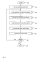
- FIG. 3 depicts a flowchart of a method of the present invention in which a DC parametric mode of an interconnect 120 acting as an input is tested.
- automated test equipment ATE
- the TAP controller of the IC 100 in a mode in which the instruction register 150 is arranged to receive the PAD_CONTROL instruction in step 320, which connects the further shift register 140 to TDI 174, after which the driver configuration data is shifted into the further shift register 140 in step 330.
- step 340 the instruction register 150 is again connected to TDI 174, and receives the instruction DC_PARAMETRIC, which connects the boundary scan shift register 130 to TDI 174, after which the boundary scan register 130 is loaded with the input data for the DC parametric test in step 350.
- step 360 the ATE provides the interconnects with input stimuli, and the response to the input stimuli is captured in the boundary scan register 130 in step 370 and subsequently shifted out of the IC 100 via TDO 175 in step 380.
- step 385 it is decided if another interconnect DC parameter is to be tested. If this is the case, the method may revert back to step 320; otherwise, the method terminates in step 390.
- FIG. 4 depicts a flowchart of a method of the present invention in which a DC parametric mode of an interconnect 120 acting as an output is tested.
- automated test equipment ATE
- the ATE brings the TAP controller of the IC 100 in a mode in which the instruction register 150 is arranged to receive the PAD_CONTROL instruction in step 420, which connects the further shift register 140 to TDI 174, after which the driver configuration data is shifted into the further shift register 140 in step 430.
- step 440 the instruction register 150 is again connected to TDI 174, and receives the instruction DC_PARAMETRIC, which connects the boundary scan shift register 130 to TDI 174, after which the boundary scan register 130 is loaded with the input data for the DC parametric test in step 450.
- the interconnects 120 have now been brought into one of the DC parametric modes as previously explained, with selected boundary scan register cells 132 providing the respective input stimuli for the interconnects 120 under test.
- the test method of the present invention has several advantages over the state of the art. For instance, because all interconnects 120 can be simultaneously switched to a logic high, a logic low or a high-impedance state, the signal stabilization or settling time of the ATE prior to a DC parametric measurement is minimized, thus reducing the overall test time and cost. Moreover, setting up the DC parametric test can be done quickly simply by feeding the appropriate test patterns in the shift registers 130 and 140, which further reduces the overall test time. In addition, the automated approach of testing the DC parameters of the interconnects 120 obviates the need for manual testing, thus reducing the risk of human error.
Landscapes
- Engineering & Computer Science (AREA)
- General Engineering & Computer Science (AREA)
- Physics & Mathematics (AREA)
- General Physics & Mathematics (AREA)
- Tests Of Electronic Circuits (AREA)
- Semiconductor Integrated Circuits (AREA)
Abstract
An integrated circuit (100) and a test method are disclosed. The IC (100 comprises a plurality of interconnections (120); and a test arrangement comprising a test access port (170) and a shift register (130) comprising a plurality of cells (132), each coupled to a respective interconnection (120) via at least one signal driver (203, 204, 205), the test arrangement further comprising a further shift register (140) comprising a plurality of cells (142) each coupled to a control terminal of a respective one of said signal drivers (203, 204, 205). This facilitates automated DC parametric testing of the interconnects (120) by shifting appropriate configuration data into the shift register (130) and the further shift register (140) respectively.
Description
- The present invention relates to an integrated circuit (IC) comprising a plurality of interconnections and a test arrangement comprising a test access port and a shift register comprising a plurality of cells, each coupled to a respective interconnection via at least one signal driver.
- The present invention further relates to a method for testing such an IC.
- Before releasing an IC into the market, an IC must be tested to ensure that the IC does not produce any errors to avoid customer returns and occurrence of potentially dangerous situations caused by unexpected IC behavior, e.g. in application domains where the IC plays an integral part in controlling a device, e.g. a car or another vehicle. Different types of errors exist. For instance, a hard error is an error caused by a physical fault such as an open, short or bridging fault. A soft error may be caused by a deviation from an intended IC design parameter, and may only occur when the IC is brought into certain modes of operation, e.g. a high-frequency operational mode. Such errors are usually more difficult to detect. An example of such an error is the failure of an external interconnection of an IC to communicate the intended signal behavior at high frequencies. Such failures may occur when an IC interconnect, e.g. a bond pad or a pin, does not exhibit the intended signal response characteristics. Such characteristics can be defined in terms of response parameters to voltage and current stimuli.
- A well-established test approach for testing IC interconnections is the IEEE 1149.1 standard, which is more commonly known as boundary scan test (BST). To this end, an IC is extended with a test arrangement including a boundary scan register which is located between the IC interconnections and the internals of the IC. In functional mode, this register is transparent such that the shift register cells do not influence the signals communicated between the IC internals and the interconnects. In a test mode, and in particular in response to the EXTEST instruction, the boundary scan register is used to communicate, i.e. provide or capture, test stimuli with the interconnects to test for the presence of interconnect faults. This test method is well-suited to detect hard errors in the interconnections, but is less suited to detect different types of parametric errors because the signal drivers that couple the shift register cells to the interconnects are kept in mode as defined in the IEEE 1149.1 standard.
- In 'Testing SoC Interconnects for Signal Integrity Using Extended JTAG Architecture' by M.H. Tehranipour et al. in Trans. Computer-Aided Design of Integrated Circuits and Systems, 23(5):800--811, May 2004, a system-on-chip architecture is disclosed in which two interconnected cores each comprise a modified boundary scan chain that are capable of generating and receiving multiple-transition test patterns to test the signal integrity of high-speed interconnections.
-
US patent No. 6,586,921 discloses an IC that has a built-in circuit for testing direct current (DC) parameters of the input and output pins of the IC. The built-in circuit is arranged to periodically sample the pin voltage to determine the magnitude and direction of the current at the pin. The test stimuli for the pins may be provided using an IEEE 1149.1-compliant boundary scan register. In order to determine the different DC parameters of the pins, the respective pin drivers are responsive to a control signal modifier circuit that is arranged to provide a driver with appropriate control signals in response to a combination of test access port (TAP) controller signals such as SHIFT-DR, UPDATE-DR and dedicated signals such as a pad test enable signal and a fast clock signal for accelerating the test clock. However, this solution has the disadvantage that the IC requires substantial amounts of additional hardware including additional pins for providing the dedicated signals. - The present invention seeks to provide an IC for which the interconnect DC parameters can be determined using less dedicated hardware.
- The present invention seeks to provide a method for testing the DC parameters of the interconnects of an IC, which requires less dedicated hardware on the IC.
- According to a first aspect of the present invention, there is provided an integrated circuit comprising a plurality of interconnections such as bond pads or pins and a test arrangement comprising a test access port and a shift register comprising a plurality of cells, each coupled to a respective interconnection via at least one signal driver, the test arrangement further comprising a further shift register comprising a plurality of cells each coupled to a control terminal of a respective one of said signal drivers.
- Hence, by shifting appropriate driver configuration data into the further shift register, the drivers between the interconnections and the cells of the shift register can be brought into any desired state, which facilitates the automated testing of different DC parameters of the interconnections using the driver appropriate configuration data and test stimuli for the interconnections.
- At least some of the cells of the further shift register may be coupled to the control terminal of more than one driver to facilitate testing blocks of drivers in the same DC mode, thus reducing the amount of shift register cells required.
- At least some further shift register cells may further be arranged to provide respective control signals to the same signal driver. This facilitates bringing a signal driver in all possible DC modes in case of a single signal driver being configurable by more than one control signal.
- In an embodiment, the test access port further comprises an instruction register and decoding logic coupled to the instruction register for connecting the shift register to a test data input in response to the presence of a first dedicated instruction in the instruction register, and for connecting the further shift register to the test data input in response to the presence of a further dedicated instruction in the instruction register. By selecting the shift register and further shift register by means of dedicated instructions, the TAP controller of the test arrangement does not need to be modified. A test apparatus may be provided comprising the dedicated instructions to control the integrated circuit during testing.
- In an embodiment, the test arrangement may be a boundary-scan compliant test arrangement.
- According to a further aspect of the present invention, there is provided a method of testing an integrated circuit according to the present invention, the method comprising connecting an external tester to the interconnections; loading a first test pattern into the shift register; loading a further test pattern into the further shift register; and determining respective parameter values of the interconnections.
- Such a method facilitates the automated testing of different DC parameters of the interconnections without requiring signal generating hardware for bringing the interconnect drivers into the required modes for measuring the DC parameters. Instead, the necessary driver configuration signals may be shifted into the further shift register in the form of a further test pattern.
- In case of the interconnections being inputs, the method may further comprise providing the interconnections with respective stimuli from the external tester, and wherein the step of determining respective parameter values of the interconnections comprises capturing said values in respective cells of the shift register. This facilitates shifting out the test results via the test data output of the test access port.
- In case of the interconnections being outputs, the step of loading a first test pattern into the shift register may comprise loading stimuli for the respective interconnections into the shift register, and the step of determining respective parameter values of the interconnections may comprise capturing said respective parameter values on the external tester. This facilitates shifting in the test stimuli via the test data input of the test access port.
- In an embodiment, the test arrangement further comprises an instruction register coupled to decoding logic for coupling a selected shift register to the test access port, the method further comprising shifting a first instruction into the instruction register to connect the shift register to a test data input for loading the first test pattern into the shift register; and shifting a further instruction into the instruction register to connect the further shift register to the test data input for loading the further test pattern into the further shift register. This embodiment ensures that the various DC parameters may be generated without requiring additional hardware for generating the driver configuration signals from the TAP control signals.
- Embodiments of the invention are described in more detail and by way of non-limiting examples with reference to the accompanying drawings, wherein
-
FIG. 1 schematically depicts an IC according to an embodiment of the present invention; -
FIG. 2 schematically depicts an aspect of the inventive IC in more detail; -
FIG. 3 schematically depicts a flowchart of an embodiment of the method of the present invention; and -
FIG. 4 schematically depicts a flowchart of another embodiment of the method of the present invention. - It should be understood that the Figures are merely schematic and are not drawn to scale. It should also be understood that the same reference numerals are used throughout the Figures to indicate the same or similar parts.
-
FIG. 1 depicts anIC 100 comprising acore 110. Thecore 110 is accessible throughinterconnects 120, e.g. bond pads or pins. The IC 100 further comprises a test arrangement including aTAP 170, which comprises a test data input (TDI) 174, a test data output (TDO) 175, a test mode select (TMS)input 171, a test clock (TCK)input 172 and a test reset (TRSTn)input 173. The test arrangement comprises a boundaryscan shift register 130, withindividual register cells 132 coupled between aninterconnect 120 and thecore 110. It is pointed out that althoughFIG. 1 shows a single boundary scanshift register cell 132 perinterconnect 120, other configurations such as multiple boundaryscan register cells 132 per interconnect 120 or interconnects 120 without boundary scan register cells in their connection to thecore 110 are equally feasible. - The
TAP 170, which may be a boundary scan test compliant TAP, further comprises aninstruction register 150 coupled todecoding logic 155. Thedecoding logic 155 is responsible for decoding instructions that are shifted into theinstruction register 150 e.g. during the SHIFT-IR mode of the state machine of the TAP controller (not shown), which are decoded for instance to provide selection signals for theinput multiplexer 182 and theoutput multiplexer 184, which are arranged to connect selected shift registers toTDI 174 andTDO 175. - The test arrangement further comprises a
further shift register 140, which has itsregister cells 142 coupled, viaconnections 144, to selected control terminals of respective signal drivers (not shown) between the boundary scanshift register cells 132 and therespective interconnects 120. - The
TAP 170 may further comprise any other shift register such as abypass register 160, or any other register which presence is mandated by the IEEE 1149.1 standard. - The
decoding logic 155 is adapted to select theboundary scan register 130 in response to a dedicated instruction 'DC_PARAMETRIC', which allows for the shifting of a test pattern into theboundary scan register 130. This test pattern is comparable to a test pattern suitable for use in the EXTEST mode. Thedecoding logic 155 is further adapted to select thefurther scan register 140 in response to a dedicated instruction 'PAD_CONTROL', which allows for the shifting of a further test pattern into thefurther scan register 140. The further test pattern is defined to provide a set of control signals to the respective drivers betweeninterconnects 120 and the boundaryscan shift register 130 such thatinterconnects 120 can be driven into different DC modes, thus facilitating an automated DC parametric test of theinterconnects 120. -
FIG. 2 shows an I/O cell of the integratedcircuit 100 in more detail. InFIG. 2 , the I/O cell 200 is a part of theboundary scan register 130. This, however, is not essential to the teachings of the present invention, and the I/O cell 200 may be a separate I/O cell. The I/O cell 200 comprisesmultiplexers decoding logic 155 for connecting the boundaryscan register cells 132 to the I/O cell 200 in response to instructions such as EXTEST and DC_PARAMETRIC. - The I/
O cell 200 typically comprises a number of drivers, e.g. amplifying buffers, non-amplifying buffers and so on, for driving signals from and to theinterconnect 120. InFIG. 2 , the I/O cell comprisesoutput signal drivers input signal driver 204. InFIG. 2 , theinterconnect 120 is a bidirectional bond pad. However, it will be appreciated that theinterconnect 120 may be an input or an output only, in which case the I/O cell 200 may be simplified. The specific embodiment of the I/O cell 200 is not essential to the present invention. The I/O cell 200 may be routinely modified by the skilled practitioner. Therefore, alternative embodiments of the I/O cell 200 are not further discussed for reasons of brevity only. - In accordance with the present invention, the drivers that can bring the
interconnect 120 into different DC parametric modes are controlled by thefurther shift register 140. InFIG. 2 , these aredrivers shift register cells 142 provide control signals ESH, P1 and P2 for the drivers of the I/O cell 200 via aconfiguration network 220. Theconfiguration network 220, which may be implemented in any suitable way, e.g. by means of a plurality ofmultiplexers decoding logic 155, is arranged to connect the control terminals of thedrivers further shift register 140 in response to the dedicated instruction PAD_CONTROL. In the absence of this instruction, theconfiguration network 220 is configured to connect these control terminals to their functional mode controllers. - Table I gives an overview of the interconnect behavior that can be induced by the control signals P1, P2 and ESH:
Table I P1 P2 ESH Interconnect behavior 0 0 X Pull-down 1 0 X Plain 0 1 X Pull-up 1 1 X Repeater X X 0 No hysteresis X X 1 Hysteresis - The value X is a don't care value. This is because the state of the
interconnect 120 caused byhysteresis driver 203 is not influenced by the pull-up/pull-downdriver 205 and vice versa. - These signals can be used to generate the following industry standard DC parametric modes on an input interconnect 120: current input at low state (IIL), current input at high state (IIH), voltage input at low state (VIL), voltage input at high state (VIH). These signals can further be used to generate the following industry standard DC parametric modes on an output interconnect 120: current output at low state (IOL), current output at high state (IOH), high-impedance current output at low state (IOZL), high-impedance current output at high state (IOZH), voltage output at low state (VOL) and voltage output at high state (VOH). All states may be generated on a
bidirectional interconnect 120.
Table II gives an overview of how the various parametric DC test modes can be invoked.Table II DC mode Input Signal 201 ESH P1 P2 IIL Low 1 X 1 0 IIH High 1 X 1 0 VIL Low 1 X 1 0 VIH High 1 X 1 0 IOL Low 0 0/1 1 0 IOH High 0 0/1 1 0 IOZL Low 1 X 1 0 IOZH High 1 X 1 0 VOL Low 0 0/1 1 0 VOH High 0 0/1 1 0 PULL-UP Low 1 X 0 0 PULL-DOWN High 1 X 0 1 REPEAT High/Low 1 X 1 1 - For different DC test modes having the same control signal configuration, the different modes are invoked by different signals provided by the ATE.
-
FIG. 3 depicts a flowchart of a method of the present invention in which a DC parametric mode of aninterconnect 120 acting as an input is tested. Upon starting the method instep 300, automated test equipment (ATE) is brought into contact with theinterconnects 120. This may for instance be achieved by means of probe needles, which may be grouped in a probe card. Next, the ATE brings the TAP controller of theIC 100 in a mode in which theinstruction register 150 is arranged to receive the PAD_CONTROL instruction instep 320, which connects thefurther shift register 140 toTDI 174, after which the driver configuration data is shifted into thefurther shift register 140 instep 330. - In
step 340, theinstruction register 150 is again connected toTDI 174, and receives the instruction DC_PARAMETRIC, which connects the boundaryscan shift register 130 toTDI 174, after which theboundary scan register 130 is loaded with the input data for the DC parametric test instep 350. - The
interconnects 120 have now been brought into one of the DC parametric modes as previously explained. Next, instep 360, the ATE provides the interconnects with input stimuli, and the response to the input stimuli is captured in theboundary scan register 130 instep 370 and subsequently shifted out of theIC 100 viaTDO 175 instep 380. Instep 385, it is decided if another interconnect DC parameter is to be tested. If this is the case, the method may revert back to step 320; otherwise, the method terminates instep 390. -
FIG. 4 depicts a flowchart of a method of the present invention in which a DC parametric mode of aninterconnect 120 acting as an output is tested. Upon starting the method instep 400, automated test equipment (ATE) is brought into contact with theinterconnects 410. Next, the ATE brings the TAP controller of theIC 100 in a mode in which theinstruction register 150 is arranged to receive the PAD_CONTROL instruction instep 420, which connects thefurther shift register 140 toTDI 174, after which the driver configuration data is shifted into thefurther shift register 140 instep 430. - In
step 440, theinstruction register 150 is again connected toTDI 174, and receives the instruction DC_PARAMETRIC, which connects the boundaryscan shift register 130 toTDI 174, after which theboundary scan register 130 is loaded with the input data for the DC parametric test instep 450. - The
interconnects 120 have now been brought into one of the DC parametric modes as previously explained, with selected boundaryscan register cells 132 providing the respective input stimuli for theinterconnects 120 under test. - Next, in
step 460, the ATE captures the response to the input stimuli, e.g. on the probe needles. Instep 465, it is decided if another interconnect DC parameter is to be tested. If this is the case, the method may revert back to step 420; otherwise, the method terminates instep 470. - The test method of the present invention has several advantages over the state of the art. For instance, because all interconnects 120 can be simultaneously switched to a logic high, a logic low or a high-impedance state, the signal stabilization or settling time of the ATE prior to a DC parametric measurement is minimized, thus reducing the overall test time and cost. Moreover, setting up the DC parametric test can be done quickly simply by feeding the appropriate test patterns in the shift registers 130 and 140, which further reduces the overall test time. In addition, the automated approach of testing the DC parameters of the
interconnects 120 obviates the need for manual testing, thus reducing the risk of human error. - It should be noted that the above-mentioned embodiments illustrate rather than limit the invention, and that those skilled in the art will be able to design many alternative embodiments without departing from the scope of the appended claims. In the claims, any reference signs placed between parentheses shall not be construed as limiting the claim. The word "comprising" does not exclude the presence of elements or steps other than those listed in a claim. The word "a" or "an" preceding an element does not exclude the presence of a plurality of such elements. The invention can be implemented by means of hardware comprising several distinct elements. In the device claim enumerating several means, several of these means can be embodied by one and the same item of hardware. The mere fact that certain measures are recited in mutually different dependent claims does not indicate that a combination of these measures cannot be used to advantage.
Claims (13)
- An integrated circuit (100) comprising:a plurality of interconnections (120); anda test arrangement comprising a test access port (170) and a shift register (130) comprising a plurality of cells (132), each coupled to a respective interconnection (120) via at least one signal driver (203, 204, 205), the test arrangement further comprising a further shift register (140) comprising a plurality of cells (142) each coupled to a control terminal of a respective one of said signal drivers (203, 204, 205).
- An integrated circuit according to claim 1, further comprising a plurality of input/output cells (200), each comprising a cell (132) of the shift register (130) and the at least one signal driver (203, 204, 205) coupling said cell (132) to the respective interconnection (120).
- An integrated circuit according to claim 1 or 2, wherein at least some further shift register cells (142) are arranged to provide respective control signals to the same signal driver (205).
- An integrated circuit according to any of the preceding claims, wherein the test access port (170) further comprises an instruction register (150) and decoding logic (155) coupled to the instruction register for connecting the shift register (130) to a test data input (174) in response to the presence of a first dedicated instruction in the instruction register (150), and for connecting the further shift register (140) to the test data input (174) in response to the presence of a further dedicated instruction in the instruction register (150).
- An integrated circuit according to claim 4, wherein said control terminals are coupled to the further shift register (140) via a configuration network (220) responsive to the decoding logic (155).
- An integrated circuit according to claim 5, wherein the configuration network (220) comprises a plurality of multiplexers (221; 222; 223).
- An integrated circuit according to any of the preceding claims, wherein the test arrangement is a boundary-scan compliant test arrangement.
- An integrated circuit according to any of the preceding claims, wherein the interconnections (120) comprise bond pads.
- A method of testing an integrated circuit comprising a plurality of interconnections (120) and a test arrangement comprising a test access port (170) and a shift register (130) comprising a plurality of cells (132), each coupled to a respective interconnection (120) via at least one signal driver (203, 204, 205), the test arrangement further comprising a further shift register (140) comprising a plurality of cells (142) each coupled to a control terminal of a respective one of said signal drivers (203, 204, 205), the method comprising:connecting (310, 410) an external tester to the interconnections;loading (320, 420) a first test pattern into the shift register;loading (340, 440) a further test pattern into the further shift register; anddetermining (370, 460) respective parameter values of the interconnections.
- A method according to claim 9, further comprising providing (360) the interconnections with respective stimuli from the external tester, and wherein the step of determining respective parameter values of the interconnections (120) comprises capturing (370) said values in respective cells (132) of the shift register (130).
- A method according to claim 9, wherein the step of loading a first test pattern into the shift register (130) comprises loading stimuli for the respective interconnections (120) into the shift register, and wherein the step of determining respective parameter values of the interconnections comprises capturing (460) said respective parameter values on the external tester.
- A method according to any of claims 9-11, wherein the test arrangement further comprises an instruction register (150) coupled to decoding logic (155) for coupling a selected shift register to a test data input (174), the method further comprising:shifting a first instruction into the instruction register (150) to connect the shift register (130) to the test data input (174) for loading the first test pattern into the shift register (130); andshifting a further instruction into the instruction register (150) to connect the further shift register (140) to the test data input (174) for loading the further test pattern into the further shift register (140).
- A test apparatus for testing the integrated circuit according to claim 4 or 5, wherein the test apparatus comprises the first dedicated instruction and the further dedicated instruction.
Priority Applications (1)
| Application Number | Priority Date | Filing Date | Title |
|---|---|---|---|
| EP08290418A EP2113779A1 (en) | 2008-04-30 | 2008-04-30 | Testable integrated circuit and integrated circuit test method |
Applications Claiming Priority (1)
| Application Number | Priority Date | Filing Date | Title |
|---|---|---|---|
| EP08290418A EP2113779A1 (en) | 2008-04-30 | 2008-04-30 | Testable integrated circuit and integrated circuit test method |
Publications (1)
| Publication Number | Publication Date |
|---|---|
| EP2113779A1 true EP2113779A1 (en) | 2009-11-04 |
Family
ID=39739976
Family Applications (1)
| Application Number | Title | Priority Date | Filing Date |
|---|---|---|---|
| EP08290418A Ceased EP2113779A1 (en) | 2008-04-30 | 2008-04-30 | Testable integrated circuit and integrated circuit test method |
Country Status (1)
| Country | Link |
|---|---|
| EP (1) | EP2113779A1 (en) |
Citations (4)
| Publication number | Priority date | Publication date | Assignee | Title |
|---|---|---|---|---|
| JP2002236142A (en) * | 2001-02-07 | 2002-08-23 | Sharp Corp | Boundary scan test circuit |
| US6586921B1 (en) | 2000-05-12 | 2003-07-01 | Logicvision, Inc. | Method and circuit for testing DC parameters of circuit input and output nodes |
| US6925583B1 (en) * | 2002-01-09 | 2005-08-02 | Xilinx, Inc. | Structure and method for writing from a JTAG device with microcontroller to a non-JTAG device |
| WO2007052090A1 (en) * | 2005-11-02 | 2007-05-10 | Freescale Semiconductor, Inc. | Device and a method for configuring input/output pads |
-
2008
- 2008-04-30 EP EP08290418A patent/EP2113779A1/en not_active Ceased
Patent Citations (4)
| Publication number | Priority date | Publication date | Assignee | Title |
|---|---|---|---|---|
| US6586921B1 (en) | 2000-05-12 | 2003-07-01 | Logicvision, Inc. | Method and circuit for testing DC parameters of circuit input and output nodes |
| JP2002236142A (en) * | 2001-02-07 | 2002-08-23 | Sharp Corp | Boundary scan test circuit |
| US6925583B1 (en) * | 2002-01-09 | 2005-08-02 | Xilinx, Inc. | Structure and method for writing from a JTAG device with microcontroller to a non-JTAG device |
| WO2007052090A1 (en) * | 2005-11-02 | 2007-05-10 | Freescale Semiconductor, Inc. | Device and a method for configuring input/output pads |
Non-Patent Citations (2)
| Title |
|---|
| DEHON A ET AL: "Automatic impedance control", SOLID-STATE CIRCUITS CONFERENCE, 1993. DIGEST OF TECHNICAL PAPERS. 40T H ISSCC., 1993 IEEE INTERNATIONAL SAN FRANCISCO, CA, USA 24-26 FEB. 1993, NEW YORK, NY, USA,IEEE, US, 24 February 1993 (1993-02-24), pages 164 - 165,283, XP010111339, ISBN: 978-0-7803-0987-6 * |
| M.H. TEHRANIPOUR ET AL.: "Testing SoC Interconnects for Signal Integrity Using Extended JTAG Architecture", TRANS. COMPUTER-AIDED DESIGN OF INTEGRATED CIRCUITS AND SYSTEMS, vol. 23, no. 5, May 2004 (2004-05-01), pages 800 - 811, XP011111805, DOI: doi:10.1109/TCAD.2004.826540 |
Similar Documents
| Publication | Publication Date | Title |
|---|---|---|
| EP1402278B1 (en) | Method and apparatus for optimized parallel testing and access of electronic circuits | |
| US11041905B2 (en) | Combinatorial serial and parallel test access port selection in a JTAG interface | |
| US6691269B2 (en) | Method for scan controlled sequential sampling of analog signals and circuit for use therewith | |
| US20030208708A1 (en) | Circuit and method for adding parametric test capability to digital boundary scan | |
| US7406641B2 (en) | Selective control of test-access ports in integrated circuits | |
| US20110179325A1 (en) | System for boundary scan register chain compression | |
| US20030046625A1 (en) | Method and apparatus for efficient control of multiple tap controllers | |
| EP3290934B1 (en) | Scan circuitry with iddq verification | |
| Ono et al. | Integrated and automated design-for-testability implementation for cell-based ICs | |
| EP2113779A1 (en) | Testable integrated circuit and integrated circuit test method | |
| US7403027B2 (en) | Apparatuses and methods for outputting signals during self-heat burn-in modes of operation | |
| US20070035321A1 (en) | Device and method for testing mixed-signal circuits | |
| KR100694315B1 (en) | Cable Delay Failure Test Controller for System-on-Chip with Multiple System Clocks and Heterogeneous Cores | |
| JP2869314B2 (en) | Boundary scan circuit, boundary scan test circuit, and method of using the same | |
| Satish | Tutorial on design for testability (DFT)" An ASIC design philosophy for testability from chips to systems" | |
| Fasang | Boundary scan and its application to analog-digital ASIC testing in a board/system environment | |
| US20250271501A1 (en) | Circuit input/output (i/o) test system | |
| US20020113614A1 (en) | Method and apparatus to enhance testability of logic coupled to IO buffers | |
| JP3588052B2 (en) | Boundary scan test circuit | |
| KR20020087931A (en) | A printed circuit assembly with configurable boundary scan paths | |
| Osseiran | Test standards (with focus on IEEE1149. 1) | |
| CN118465500A (en) | Chip testing device and storage medium | |
| Al-Khalifa | A Test Procedure for Boundary Scan Circuitry in PLDs and FPGAs. | |
| Parker | Design for Boundary-Scan Test | |
| Semiconductor | Non-Contact Test Access for Surface Mount Technology IEEE |
Legal Events
| Date | Code | Title | Description |
|---|---|---|---|
| PUAI | Public reference made under article 153(3) epc to a published international application that has entered the european phase |
Free format text: ORIGINAL CODE: 0009012 |
|
| AK | Designated contracting states |
Kind code of ref document: A1 Designated state(s): AT BE BG CH CY CZ DE DK EE ES FI FR GB GR HR HU IE IS IT LI LT LU LV MC MT NL NO PL PT RO SE SI SK TR |
|
| AX | Request for extension of the european patent |
Extension state: AL BA MK RS |
|
| STAA | Information on the status of an ep patent application or granted ep patent |
Free format text: STATUS: THE APPLICATION HAS BEEN REFUSED |
|
| 18R | Application refused |
Effective date: 20091121 |