EP2110956A2 - Single-chip wireless transceiver - Google Patents
Single-chip wireless transceiver Download PDFInfo
- Publication number
- EP2110956A2 EP2110956A2 EP08008209A EP08008209A EP2110956A2 EP 2110956 A2 EP2110956 A2 EP 2110956A2 EP 08008209 A EP08008209 A EP 08008209A EP 08008209 A EP08008209 A EP 08008209A EP 2110956 A2 EP2110956 A2 EP 2110956A2
- Authority
- EP
- European Patent Office
- Prior art keywords
- mimo
- radio
- module
- stages
- control
- Prior art date
- Legal status (The legal status is an assumption and is not a legal conclusion. Google has not performed a legal analysis and makes no representation as to the accuracy of the status listed.)
- Ceased
Links
Images



Classifications
-
- H—ELECTRICITY
- H04—ELECTRIC COMMUNICATION TECHNIQUE
- H04B—TRANSMISSION
- H04B7/00—Radio transmission systems, i.e. using radiation field
- H04B7/02—Diversity systems; Multi-antenna system, i.e. transmission or reception using multiple antennas
-
- H—ELECTRICITY
- H04—ELECTRIC COMMUNICATION TECHNIQUE
- H04B—TRANSMISSION
- H04B7/00—Radio transmission systems, i.e. using radiation field
- H04B7/02—Diversity systems; Multi-antenna system, i.e. transmission or reception using multiple antennas
- H04B7/04—Diversity systems; Multi-antenna system, i.e. transmission or reception using multiple antennas using two or more spaced independent antennas
- H04B7/0413—MIMO systems
-
- H—ELECTRICITY
- H04—ELECTRIC COMMUNICATION TECHNIQUE
- H04B—TRANSMISSION
- H04B1/00—Details of transmission systems, not covered by a single one of groups H04B3/00 - H04B13/00; Details of transmission systems not characterised by the medium used for transmission
- H04B1/06—Receivers
- H04B1/16—Circuits
Definitions
- the present invention relates generally to wireless communications, and more particularly to a wireless transceiver.
- MIMO Multiple-input-multiple-output
- Embodiments of a wireless transceiver are provided herein. Embodiments can be used in multiple-input-multiple-output (MIMO) wireless transceivers.
- radio control signal bundles are provided as direct parallel interconnects between digital signal processing modules and the radio module of the wireless transceiver to enable a precise low-latency control of radio functions.
- a separate physical line is provided to control each radio setting of the radio module, thereby enabling simultaneous real-time control of any number of radio settings.
- the various digital and analog components of the wireless transceiver are integrated within a single chip of the same process technology.
- an integrated circuit is provided, comprising:
- FIG. 1 illustrates an example multiple-input-multiple-output (MIMO) communication system.
- MIMO multiple-input-multiple-output
- FIG. 2 illustrates an example MIMO wireless transceiver.
- FIG. 3 illustrates another example MIMO wireless transceiver.
- FIG. 4 illustrates a single-chip wireless transceiver.
- FIG. 1 illustrates an example multiple-input multiple-output (MIMO) communication system 100.
- Communication system 100 includes transceivers A and B and a communication channel 170.
- Transceiver A includes a transmitter 110. Transceiver A may also include a receiver (not shown). Transmitter 110 includes multiple transmit antennas 130- ⁇ 1,...,n ⁇ . Transceiver B includes a receiver 120. Transceiver B may also include a transmitter (not shown). Receiver 120 includes multiple receive antennas 160- ⁇ 1,...,m ⁇ . The number of transmit antennas (n) of transmitter 110 and the number of receive antennas (m) of receiver 120 may or may not be equal.
- Communication channel 170 represents a MIMO channel. Accordingly, communication channel 170 includes multiple spatial sub-channels formed between multiple transmit antennas 130- ⁇ 1,...,n ⁇ and multiple receive antennas 160- ⁇ 1,...,m ⁇ . Typically, the number of spatial sub-channels comprised in a MIMO communication channel is related to a channel matrix H of the communication channel, which associates a complex gain (amplitude attenuation factor and a phase shift) with each spatial sub-channel.
- H AB represents the channel matrix from transmitter 110 to receiver 120 of communication channel 170.
- signals 140- ⁇ 1,...,n ⁇ represent signals transmitted by respective transmit antennas 130- ⁇ 1,...,n ⁇ of transmitter 110.
- Signals 140- ⁇ 1,...,n ⁇ may be transmitted with equal or different transmit power levels.
- signals 140- ⁇ 1,...,n ⁇ propagate in different propagation paths from transmitter 110 to receiver 120 and thus experience different channel effects.
- signals 140- ⁇ 1,...,n ⁇ recombine to generate received signals 150- ⁇ 1,...,m ⁇ at respective receive antennas 160 ⁇ 1,...,m ⁇ .
- Received signals 150- ⁇ 1,...,m ⁇ may be received at equal or different power levels. Further, received signals 150- ⁇ 1,...,m ⁇ may be received at equal or different instants of time.
- FIG. 2 illustrates an example MIMO wireless transceiver 200.
- Wireless transceiver 200 can be used in a wireless local area network (WLAN) environment, such as 802.11n.
- WLAN wireless local area network
- Wireless transceiver 200 includes a baseband integrated circuit (IC) 202, a radio IC 222, front end components 248, and a plurality of antennas 250a-n.
- IC baseband integrated circuit
- Baseband IC 202 includes a Digital Signal Processing (DSP) module 204, an Analog Front End (AFE) module 206, and a Host Interface 208.
- DSP Digital Signal Processing
- AFE Analog Front End
- DSP module 204 includes a MIMO Transmit module 212, a MIMO receive module 214, and a control logic module 216.
- Control and Data signals connect control logic module 216 with each of MIMO Transmit module 212 and MIMO receive module 214.
- AFE module 206 includes a plurality of Digital-to-Analog Converters (DACs) 218a-b and Analog-to-Digital Converters (ADCs) 220a-b.
- DACs Digital-to-Analog Converters
- ADCs Analog-to-Digital Converters
- AFE module 206 is illustrated with only two DACs and two ADCs. However, as would be understood by a person skilled in the art based on the teachings herein, AFE module 206 can include any number of DACs and ADCs.
- Host Interface 208 is an interface between a host processor (not shown) and DSP module 204. As such, host interface 208 communicates via a data and control bus 210 with the host processor and via data bus 252 and control bus 254 with control logic module 216. Typically, host interface 208 is a multi-GHz interface with a clock speed comparable to that of the processor and much higher than that of DSP module 204. In another embodiment, host interface 208 can include an embedded Host Processor instead of merely being an interface to a host processor located outside of the chip. A host processor generally carries out higher layer protocol tasks, including tasks related to medium access control (MAC), rate control (adaptation of the transmission speed parameters over the air), TCP/IP, and radio calibration control.
- MAC medium access control
- rate control adaptive rate control
- Radio IC 222 includes a plurality of transmitter units 224a-b, a plurality of receive units 226a-b, a synthesizer module 228, and a radio control de-multiplexer 230.
- Radio IC 222 is illustrated with only two transmitter units and two receiver units. However, as would be understood by a person skilled in the art based on the teachings herein, radio IC 222 can include any number of transmitter units and receiver units.
- Transmitter units 224a-b each includes at least one of (a) one or more frequency up-conversion stages; (b) one or more variable gain amplification stages; (c) one or more variable bandwidth filtering stages; and (d) circuitry to selectively enable/disable the frequency up-conversion, amplification, and filtering stages.
- receiver units 226a-b each includes at least one of (e) one or more frequency down-conversion stages; (f) one or more variable gain amplification stages; (g) one or more variable bandwidth filtering stages; and (h) circuitry to selectively enable/disable said frequency down-conversion, amplification, and filtering stages.
- Synthesizer module 228 generates and provides frequency conversion signals to the frequency up-conversion stages of transmitter units 224a-b and the frequency down-conversion stages of receiver units 226a-b.
- MIMO Transmit module 212 In the transmit mode of wireless transceiver 200, MIMO Transmit module 212 generates digital streams from received information. The digital streams are converted by DACs 218a-b into transmit analog signals, which are forwarded over circuit lines 236a-b to transmitter units 224a-b of radio IC 222. In the receive mode, analog signals are received by receive units 226a-b of radio IC 222 and are forwarded over circuit lines 238a-b to baseband IC 202. At baseband IC 202, ADCs 220a-b convert the analog signals to digital signals, which are then transferred to MIMO Receive module 214.
- Circuit lines 236a-b and 238a-b are printed lines over the circuit board where baseband IC 202 and radio IC 222 are co-located. As such, driver-matching circuitry are needed at the ends of circuit lines 236 or 238 to generate sufficient driving power to forward the analog signals with low noise, low interference, and low latency between radio IC 222 and baseband IC 202.
- Driver-matching circuitry are illustrated using reference numerals 232a-d and 234a-d over circuit lines 236 and 238, respectively.
- the driver-matching circuitry found at the ends of circuit lines 236 and 238 may also include voltage conversion devices to ensure reliable signal transfer.
- each transmit signal driven between baseband IC 202 and a respective transmitter unit 224 of radio IC 222 includes four circuit lines, with two differential circuit lines for each of the real part (In-phase) and the imaginary part (Quadrature phase) of the complex signal.
- receive signals driven between receive units 226 and baseband IC 202 each includes four circuit lines.
- radio control signals are also sent between baseband IC 202 and radio IC 222. This is illustrated using radio control signal 240, which is used to transmit control information between baseband IC 202 and the radio components of radio IC 222, including transmitter units 224a-b, receiver units 226a-b, and synthesizer module 228. As with transmit and receive data signals 236a-b and 238a-b, driver-matching circuitry 242a-b are used at both ends of control signal 240.
- radio control information transmitted over radio control signal 240 is received by radio control de-multiplexer 230 of radio IC 222.
- Radio control de-multiplexer 230 forwards the received control information to its intended recipient among transmitter units 224a-b, receiver units 226a-b, and synthesizer 228 via signal lines 246a-e.
- latches 244a-e are needed to maintain the state of control signal 240 for a given radio unit, while radio control signal 240 can be used to transmit control information for another radio unit in a subsequent time slot.
- radio transceivers that support high data rates require a tight control of radio settings, including control of amplifier gains, filter bandwidths, and power-up/down events.
- transmit chains of radio transceivers often have multiple gain stages, whose gains need to be carefully set to achieve high signal quality and to meet transmit power requirements.
- receive chains also have multiple gain stages that need to be adjusted in order to reliably receive incoming signals with minimal signal integrity loss.
- control of the transmit and receive gains need to occur in real-time and with very small latency (e.g., 100 nanoseconds or less) in order to timely complete time-critical events.
- very small latency e.g. 100 nanoseconds or less
- the frame needs to be carrier-detected (or carrier-sensed, CRS) and all receive gains have to be optimally adjusted using gain-control steps (GCT) within an overall time period of 6-8 microseconds.
- GCT gain-control steps
- 802.11n is characterized by a complex signaling structure that specifies different signaling bandwidths (e.g., 20 and 40 MHz) and that requires backward compatibility with standards such as 802.11, 802.11a, 802.11b, and 802.11g. As such, depending on the signal structure that is transmitted or received, filtering parameters have to be adjusted in real-time to adjust the transceiver for optimal signal transmission or reception.
- a large number of pins and circuit lines between baseband IC 202 and radio IC 222 will be needed. This is particularly true in the case of MIMO transceivers, which include large numbers of transmitter and receiver units.
- the transceiver design becomes high in cost and power consumption.
- signal quality can be impacted.
- the driver-matching circuitry can cause an increase in the latency of the real-time control signals.
- the driver-matching circuitry cause an increase in heat generation in the radio IC, particularly when a power amplifier (PA) is integrated within the radio IC, leading to an increase in thermal noise and distortion and interfering with the integrity of incoming and/or outgoing signals.
- PA power amplifier
- the degradation in the real-time control of radio components of radio IC 222 becomes even more stringent when more than two transmitter and/or receiver radio units are used.
- the number of desired interconnects increases proportionally as a function of the number of transmitter and receiver units in radio IC 222 at the rate of 4*(N+M), where N is the number of transmitter units and M is the number of receiver units of radio IC 222.
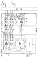
- FIG. 3 illustrates another example MIMO wireless transceiver 300.
- Wireless transceiver 300 includes a MIMO integrated circuit (IC) 302, front end components 248, and a plurality of antennas 250a-n.
- IC MIMO integrated circuit
- MIMO IC 302 includes a MIMO Digital Signal Processing (DSP) module 304, a MIMO radio module 322, and a host processor interface 208, all integrated within a single integrated circuit using the same process technology.
- DSP Digital Signal Processing
- MIMO radio module 322 includes a MIMO radio module 302.
- host processor interface 208 all integrated within a single integrated circuit using the same process technology.
- CMOS process technology is used.
- MIMO DSP module 304 includes a MIMO Transmit module 312, a MIMO receive module 314, and a control logic module 316.
- MIMO Transmit module 312, MIMO Receive module 314, and control logic module 316 are structurally and functionally similar to MIMO Transmit module 212, MIMO Receive module 214, and control logic module 216, respectively, of wireless transceiver 200.
- MIMO radio module 322 includes a plurality of transmitter units 324a-b, a plurality of receiver units 326a-b, and a synthesizer module 328.
- Transmitter units 324a-b, receiver units 326a-b, and synthesizer module 328 are structurally and functionally similar to transmitter units 224a-b, receiver units 226a-b, and synthesizer module 228, respectively, of wireless transceiver 200.
- transmitter units 324a-b each includes an integrated power amplifier (PA) stage.
- PA integrated power amplifier
- an Analog Front End (AFE) module 306 including a plurality of Digital-to-Analog Converters (DACs) 318a-b and Analog-to-Digital Converters (ADCs) 320a-b, is used to convert from digital to analog (from analog to digital) transmit data signals 330a-b (receive data signals 332a-b) between MIMO DSP module 304 and MIMO radio module 322.
- AFE Analog Front End
- MIMO IC 302 further includes a plurality of radio control signal bundles 334a-e that couple control logic module 316 with respective ones of transmitter units 324a-b, receiver units 326a-b, and synthesizer module 328.
- radio control signal bundles 334a-e include a plurality of transmit radio control signal bundles 334a-b, a plurality of receive radio control signal bundles 334c-d, and a synthesizer radio control signal bundle 334e.
- Each of transmit radio control signal bundles 334a-b includes control signals to control respective stages (e.g., frequency conversion stages, gain, etc.) of a corresponding transmitter unit of MIMO radio module 322.
- each of receive radio control signal bundles 334c-d includes control signals to control respective stages of a corresponding receiver unit of MIMO radio module 322.
- Synthesizer radio control signal bundle 334e includes control signals to control respective stages of synthesizer module 328.
- radio control signal bundles 334a-e are direct parallel interconnects between control logic module 316 and MIMO radio module 322, providing a separate physical line for each radio setting of each transmitter and receiver unit.
- radio control signal bundles 334a-e enable MIMO DSP module 304 to simultaneously control in real-time any one of transmitter units 324a-b, receiver units 326a-b, and synthesizer module 328.
- the higher efficiency of these direct interconnects enable a large number of interconnects per radio (transmitter/receiver) unit, thereby increasing the precision with which radio functions can be adjusted.
- radio control signal bundles 334a-e enable a tight and precise low-latency real-time control of all radio settings of MIMO radio module 322. Furthermore, by using the same process technology for the various digital and analog components of wireless transceiver 300 and thereby eliminating inter-chip circuit lines (e.g., circuit lines 236a-b in wireless transceiver 200), several components can be eliminated. For example, driver-matching circuitry and voltage conversion circuitry are no longer needed. In addition, with a parallel radio control approach, de-multiplexing and latching circuitry (e.g., radio control de-multiplexer 230 and latches 244a-e) can also be eliminated. This reduction in components correspondingly results in a reduced cost and power consumption transceiver design.
- de-multiplexing and latching circuitry e.g., radio control de-multiplexer 230 and latches 244a-e
- the wireless IEEE 802.11n standard describes MIMO systems up to four spatial streams.
- the number of supported transmitter and receiver units may vary as well as the number of baseband signals supported between the DSP and the radio blocks. This depends on the modes of operation according to the standard that are supported by the particular embodiment. For instance, the number of transmitter units can be two and the number of receiver units can be three. This is referred to as a 2x3 embodiment. Other embodiments may be possible including, for example, 2x1, 1x2, 2x2, 2x4, 3x2, 3x3, 3x4, 4x2, 4x3, 4x4, etc.
- the integration of the DSP and the radio modules onto the same substrate allows the radio to more effectively transport heat away from sensitive analog components, thereby increasing signal quality.
- circuit material such as CMOS have a higher heat conductivity than air. Therefore, heat generated in the radio module can readily travel to other, non-radio components (e.g., DSP, Host interface, etc.) on the integrated transceiver, thereby increasing the effective area for radio heat drain-off.
- FIG. 4 illustrates a single-chip wireless transceiver 400.
- Wireless transceiver 400 includes one or more High-speed Host Interfaces 404, one or more Digital Signal Processing (DSP) blocks 406, and a radio module 408, all integrated on a single die 402.
- module 404 not only includes interfaces to external hosts, such as host processors located outside of the IC, but also includes one or more complete embedded (host) processors, such as an ARM (Advanced RISC Machine) processor with state-of-the-art peripheries and program memory.
- host such as host processors located outside of the IC
- ARM Advanced RISC Machine
- Such an embodiment is particularly useful for embedded applications, such as cell phones, small portable devices, or other devices not connected to a personal computer and having a host that is relied upon for processing of higher communication layers.
- High-speed interfaces 404 may include host processor interfaces such as host processor interface 208.
- DSP blocks 406 may include digital modules such as MIMO DSP module 304 among others, including MIMO-PHY, MAC, and Control logic modules.
- Radio module 408 may include analog modules such as MIMO radio module 322 of wireless transceiver 300.
- DSP blocks 406 are positioned between high-speed interfaces 404 and radio module 408. As such, a maximum or near maximum distance is provided between the analog components of radio module 408 and the high-speed digital components of high-speed interfaces 404.
- high-speed interfaces 404, DSP blocks 406, and radio module 408 are positioned to minimize the lengths of signal interconnects between DSP blocks 406 and radio module 408.
- high-speed interfaces 404, DSP blocks 406, and radio module 408 are positioned to increase the effective heat drain-off area of the radio module.
Landscapes
- Engineering & Computer Science (AREA)
- Computer Networks & Wireless Communication (AREA)
- Signal Processing (AREA)
- Transceivers (AREA)
- Radio Transmission System (AREA)
Abstract
Description
- The present application claims the benefit of
U.S. Provisional Patent Application No. 60/929,160, filed June 15, 2007 - The present invention relates generally to wireless communications, and more particularly to a wireless transceiver.
- Multiple-input-multiple-output (MIMO) is a wireless communications technology that simultaneously uses multiple spatial sub-channels formed between multiple transmit antennas and multiple receive antennas to transmit signals between wireless transceivers.
- Accordingly, precise real-time control of radio settings in the wireless transceivers is needed to efficiently receive and recombine received signals into information signals. For example, real-time control is needed of gain stages, filter bandwidths, and power-up/down functions of radio components of the wireless transceiver.
- Conventional wireless transceivers provide a degraded ability of real-time radio control. This degradation becomes even more stringent when more than two transmitter and/or receiver radio units are used in the wireless transceiver.
- Therefore, an improved approach to the real-time control of radio components in wireless transceivers, and particularly in MIMO wireless transceivers, is needed.
- Embodiments of a wireless transceiver are provided herein. Embodiments can be used in multiple-input-multiple-output (MIMO) wireless transceivers. In an embodiment, radio control signal bundles are provided as direct parallel interconnects between digital signal processing modules and the radio module of the wireless transceiver to enable a precise low-latency control of radio functions. In another embodiment, a separate physical line is provided to control each radio setting of the radio module, thereby enabling simultaneous real-time control of any number of radio settings. In a further embodiment, the various digital and analog components of the wireless transceiver are integrated within a single chip of the same process technology.
According to an aspect of the invention, an integrated circuit (IC) is provided, comprising: - a multiple-input-multiple-output (MIMO) radio module, including a plurality of transmitter and receiver units;
- a MIMO digital signal processing (DSP) module; and
- a host processor interface;
- a plurality of transmit radio control signal bundles, each of said transmit control signal bundles comprising control signals to control respective stages of a corresponding transmitter unit of said MIMO radio module;
- a plurality of receive radio control signal bundles, each of said receive control signal bundles comprising control signals to control respective stages of a corresponding receiver unit of said MIMO radio module; and
- a synthesizer radio control signal bundle comprising control signals to control respective stages of said synthesizer module.
- a multiple-input-multiple-output (MIMO) radio module, including a plurality of transmitter and receiver units;
- a MIMO digital signal processing (DSP) module; and
- an embedded host processor;
- Further embodiments, features, and advantages of the present invention, as well as the structure and operation of the various embodiments of the present invention, are described in detail below with reference to the accompanying drawings.
- The accompanying drawings, which are incorporated herein and form a part of the specification, illustrate the present invention and, together with the description, further serve to explain the principles of the invention and to enable a person skilled in the pertinent art to make and use the invention.
-
FIG. 1 illustrates an example multiple-input-multiple-output (MIMO) communication system. -
FIG. 2 illustrates an example MIMO wireless transceiver. -
FIG. 3 illustrates another example MIMO wireless transceiver. -
FIG. 4 illustrates a single-chip wireless transceiver. - The present invention will be described with reference to the accompanying drawings. Generally, the drawing in which an element first appears is typically indicated by the leftmost digit(s) in the corresponding reference number.
-
FIG. 1 illustrates an example multiple-input multiple-output (MIMO)communication system 100.Communication system 100 includes transceivers A and B and acommunication channel 170. - Transceiver A includes a
transmitter 110. Transceiver A may also include a receiver (not shown).Transmitter 110 includes multiple transmit antennas 130-{1,...,n}. Transceiver B includes areceiver 120. Transceiver B may also include a transmitter (not shown).Receiver 120 includes multiple receive antennas 160-{1,...,m}. The number of transmit antennas (n) oftransmitter 110 and the number of receive antennas (m) ofreceiver 120 may or may not be equal. -
Communication channel 170 represents a MIMO channel. Accordingly,communication channel 170 includes multiple spatial sub-channels formed between multiple transmit antennas 130-{1,...,n} and multiple receive antennas 160-{1,...,m}. Typically, the number of spatial sub-channels comprised in a MIMO communication channel is related to a channel matrix H of the communication channel, which associates a complex gain (amplitude attenuation factor and a phase shift) with each spatial sub-channel. - Referring to the example of
FIG. 1 , HAB represents the channel matrix fromtransmitter 110 toreceiver 120 ofcommunication channel 170. - Still referring to
FIG. 1 , signals 140-{1,...,n} represent signals transmitted by respective transmit antennas 130-{1,...,n} oftransmitter 110. Signals 140-{1,...,n} may be transmitted with equal or different transmit power levels. As illustrated inFIG. 1 , signals 140-{1,...,n} propagate in different propagation paths fromtransmitter 110 toreceiver 120 and thus experience different channel effects. Atreceiver 120, signals 140-{1,...,n} recombine to generate received signals 150-{1,...,m} at respective receive antennas 160{1,...,m}. Received signals 150-{1,...,m} may be received at equal or different power levels. Further, received signals 150-{1,...,m} may be received at equal or different instants of time. -
FIG. 2 illustrates an exampleMIMO wireless transceiver 200.Wireless transceiver 200 can be used in a wireless local area network (WLAN) environment, such as 802.11n. -
Wireless transceiver 200 includes a baseband integrated circuit (IC) 202, aradio IC 222,front end components 248, and a plurality ofantennas 250a-n. -
Baseband IC 202 includes a Digital Signal Processing (DSP)module 204, an Analog Front End (AFE)module 206, and aHost Interface 208. -
DSP module 204 includes a MIMO Transmitmodule 212, a MIMO receivemodule 214, and acontrol logic module 216. Control and Data signals connectcontrol logic module 216 with each of MIMO Transmitmodule 212 and MIMO receivemodule 214. -
AFE module 206 includes a plurality of Digital-to-Analog Converters (DACs) 218a-b and Analog-to-Digital Converters (ADCs) 220a-b. For the ease of illustration,AFE module 206 is illustrated with only two DACs and two ADCs. However, as would be understood by a person skilled in the art based on the teachings herein,AFE module 206 can include any number of DACs and ADCs. -
Host Interface 208 is an interface between a host processor (not shown) andDSP module 204. As such,host interface 208 communicates via a data andcontrol bus 210 with the host processor and viadata bus 252 and control bus 254 withcontrol logic module 216. Typically,host interface 208 is a multi-GHz interface with a clock speed comparable to that of the processor and much higher than that ofDSP module 204. In another embodiment,host interface 208 can include an embedded Host Processor instead of merely being an interface to a host processor located outside of the chip. A host processor generally carries out higher layer protocol tasks, including tasks related to medium access control (MAC), rate control (adaptation of the transmission speed parameters over the air), TCP/IP, and radio calibration control. -
Radio IC 222 includes a plurality oftransmitter units 224a-b, a plurality of receiveunits 226a-b, asynthesizer module 228, and aradio control de-multiplexer 230. For the ease of illustration,Radio IC 222 is illustrated with only two transmitter units and two receiver units. However, as would be understood by a person skilled in the art based on the teachings herein,radio IC 222 can include any number of transmitter units and receiver units. -
Transmitter units 224a-b each includes at least one of (a) one or more frequency up-conversion stages; (b) one or more variable gain amplification stages; (c) one or more variable bandwidth filtering stages; and (d) circuitry to selectively enable/disable the frequency up-conversion, amplification, and filtering stages. Similarly,receiver units 226a-b each includes at least one of (e) one or more frequency down-conversion stages; (f) one or more variable gain amplification stages; (g) one or more variable bandwidth filtering stages; and (h) circuitry to selectively enable/disable said frequency down-conversion, amplification, and filtering stages. -
Synthesizer module 228 generates and provides frequency conversion signals to the frequency up-conversion stages oftransmitter units 224a-b and the frequency down-conversion stages ofreceiver units 226a-b. - In the transmit mode of
wireless transceiver 200, MIMO Transmitmodule 212 generates digital streams from received information. The digital streams are converted byDACs 218a-b into transmit analog signals, which are forwarded overcircuit lines 236a-b totransmitter units 224a-b ofradio IC 222. In the receive mode, analog signals are received by receiveunits 226a-b ofradio IC 222 and are forwarded overcircuit lines 238a-b to basebandIC 202. Atbaseband IC 202,ADCs 220a-b convert the analog signals to digital signals, which are then transferred to MIMO Receivemodule 214. -
Circuit lines 236a-b and 238a-b are printed lines over the circuit board wherebaseband IC 202 andradio IC 222 are co-located. As such, driver-matching circuitry are needed at the ends of circuit lines 236 or 238 to generate sufficient driving power to forward the analog signals with low noise, low interference, and low latency betweenradio IC 222 andbaseband IC 202. Driver-matching circuitry are illustrated usingreference numerals 232a-d and 234a-d over circuit lines 236 and 238, respectively. Generally, sincebaseband IC 202 andradio IC 222 are based on different process technologies (e.g., CMOS versus SiGe), the driver-matching circuitry found at the ends of circuit lines 236 and 238 may also include voltage conversion devices to ensure reliable signal transfer. - It is noted that in conventional transceivers, which use a complex signal representation of bandpass signals, each transmit signal driven between
baseband IC 202 and a respective transmitter unit 224 ofradio IC 222 includes four circuit lines, with two differential circuit lines for each of the real part (In-phase) and the imaginary part (Quadrature phase) of the complex signal. Similarly, receive signals driven between receive units 226 andbaseband IC 202 each includes four circuit lines. - In addition to data signals, radio control signals are also sent between
baseband IC 202 andradio IC 222. This is illustrated using radio control signal 240, which is used to transmit control information betweenbaseband IC 202 and the radio components ofradio IC 222, includingtransmitter units 224a-b,receiver units 226a-b, andsynthesizer module 228. As with transmit and receivedata signals 236a-b and 238a-b, driver-matchingcircuitry 242a-b are used at both ends of control signal 240. - In
wireless transceiver 200, radio control information transmitted over radio control signal 240 is received byradio control de-multiplexer 230 ofradio IC 222.Radio control de-multiplexer 230 forwards the received control information to its intended recipient amongtransmitter units 224a-b,receiver units 226a-b, andsynthesizer 228 viasignal lines 246a-e. As such, latches 244a-e are needed to maintain the state of control signal 240 for a given radio unit, while radio control signal 240 can be used to transmit control information for another radio unit in a subsequent time slot. - Typically, radio transceivers that support high data rates require a tight control of radio settings, including control of amplifier gains, filter bandwidths, and power-up/down events.
- For example, transmit chains of radio transceivers often have multiple gain stages, whose gains need to be carefully set to achieve high signal quality and to meet transmit power requirements. Similarly, receive chains also have multiple gain stages that need to be adjusted in order to reliably receive incoming signals with minimal signal integrity loss. Further, the control of the transmit and receive gains need to occur in real-time and with very small latency (e.g., 100 nanoseconds or less) in order to timely complete time-critical events. For example, in the case of an OFDM frame according to 802.11 a or 802.1 In, the frame needs to be carrier-detected (or carrier-sensed, CRS) and all receive gains have to be optimally adjusted using gain-control steps (GCT) within an overall time period of 6-8 microseconds.
- In addition to gain control, real-time filter bandwidth control is also needed. For example, 802.11n is characterized by a complex signaling structure that specifies different signaling bandwidths (e.g., 20 and 40 MHz) and that requires backward compatibility with standards such as 802.11, 802.11a, 802.11b, and 802.11g. As such, depending on the signal structure that is transmitted or received, filtering parameters have to be adjusted in real-time to adjust the transceiver for optimal signal transmission or reception.
- Similarly, real-time control is needed of power-up/down functions of the radio components to reduce power consumption and potential interference between the components.
- Accordingly, a high degree of direct controllability through circuit lines between
baseband IC 202 andradio IC 222 is desired to achieve the above described real-time controls. This, however, is both challenging and cost inefficient to implement in wireless transceiver designs such aswireless transceiver 200. - In one aspect, a large number of pins and circuit lines between
baseband IC 202 andradio IC 222 will be needed. This is particularly true in the case of MIMO transceivers, which include large numbers of transmitter and receiver units. As such, with driver-matching circuitry needed for each circuit line, the transceiver design becomes high in cost and power consumption. In addition, signal quality can be impacted. For example, due to the inductive and/or capacitive characteristics of circuit lines, the driver-matching circuitry can cause an increase in the latency of the real-time control signals. Further, the driver-matching circuitry cause an increase in heat generation in the radio IC, particularly when a power amplifier (PA) is integrated within the radio IC, leading to an increase in thermal noise and distortion and interfering with the integrity of incoming and/or outgoing signals. - All these factors result in a limited number of possible interconnects between
baseband IC 202 andradio IC 222, which causes a time-multiplexed approach to the control of radio components ofradio IC 222. This degrades the ability ofbaseband IC 202 to control in real-time radio components ofradio IC 222. For example, due to the use of fewer than desired interconnects betweenbaseband IC 202 andradio IC 222, the number of gain stages that can be individually adjusted at any given time is limited. Similarly, lower flexibility in real-time bandwidth adjustment and in the real-time control of power-up/down functions of radio components is achieved. - The degradation in the real-time control of radio components of
radio IC 222 becomes even more stringent when more than two transmitter and/or receiver radio units are used. For example, in conventional transceivers, the number of desired interconnects increases proportionally as a function of the number of transmitter and receiver units inradio IC 222 at the rate of 4*(N+M), where N is the number of transmitter units and M is the number of receiver units ofradio IC 222. - Accordingly, in practice, only a limited number of radio settings can be adjusted in real-time at any given time and a time-multiplexed approach to real-time control, as illustrated in
wireless transceiver 200 usingradio control de-multiplexer 230, is used. These drawbacks result in signal integrity deterioration through delayed signaling and increased impairments due to higher thermal noise and/or distortion, which is particularly disadvantageous in the context of MIMO systems, which require higher signal-to-noise-and-distortion ratios and signal-to-interference ratios for proper reconstruction of transmitted data sequences. - Therefore, an improved approach to the real-time control of radio components in wireless transceivers, and particularly in MIMO wireless transceivers, is needed.
-
FIG. 3 illustrates another exampleMIMO wireless transceiver 300.Wireless transceiver 300 includes a MIMO integrated circuit (IC) 302,front end components 248, and a plurality ofantennas 250a-n. -
MIMO IC 302 includes a MIMO Digital Signal Processing (DSP)module 304, aMIMO radio module 322, and ahost processor interface 208, all integrated within a single integrated circuit using the same process technology. In an embodiment, a CMOS process technology is used. -
MIMO DSP module 304 includes a MIMO Transmit module 312, a MIMO receivemodule 314, and acontrol logic module 316. MIMO Transmit module 312, MIMO Receivemodule 314, and controllogic module 316 are structurally and functionally similar to MIMO Transmitmodule 212, MIMO Receivemodule 214, and controllogic module 216, respectively, ofwireless transceiver 200. -
MIMO radio module 322 includes a plurality oftransmitter units 324a-b, a plurality ofreceiver units 326a-b, and asynthesizer module 328.Transmitter units 324a-b,receiver units 326a-b, andsynthesizer module 328 are structurally and functionally similar totransmitter units 224a-b,receiver units 226a-b, andsynthesizer module 228, respectively, ofwireless transceiver 200. In an embodiment,transmitter units 324a-b each includes an integrated power amplifier (PA) stage. - As in
wireless transceiver 200, an Analog Front End (AFE)module 306, including a plurality of Digital-to-Analog Converters (DACs) 318a-b and Analog-to-Digital Converters (ADCs) 320a-b, is used to convert from digital to analog (from analog to digital) transmitdata signals 330a-b (receivedata signals 332a-b) betweenMIMO DSP module 304 andMIMO radio module 322. -
MIMO IC 302 further includes a plurality of radiocontrol signal bundles 334a-e that couplecontrol logic module 316 with respective ones oftransmitter units 324a-b,receiver units 326a-b, andsynthesizer module 328. In an embodiment, radiocontrol signal bundles 334a-e include a plurality of transmit radiocontrol signal bundles 334a-b, a plurality of receive radio control signal bundles 334c-d, and a synthesizer radiocontrol signal bundle 334e. Each of transmit radiocontrol signal bundles 334a-b includes control signals to control respective stages (e.g., frequency conversion stages, gain, etc.) of a corresponding transmitter unit ofMIMO radio module 322. Similarly, each of receive radio control signal bundles 334c-d includes control signals to control respective stages of a corresponding receiver unit ofMIMO radio module 322. Synthesizer radiocontrol signal bundle 334e includes control signals to control respective stages ofsynthesizer module 328. - In an embodiment, radio
control signal bundles 334a-e are direct parallel interconnects betweencontrol logic module 316 andMIMO radio module 322, providing a separate physical line for each radio setting of each transmitter and receiver unit. As such, radiocontrol signal bundles 334a-e enableMIMO DSP module 304 to simultaneously control in real-time any one oftransmitter units 324a-b,receiver units 326a-b, andsynthesizer module 328. Furthermore, the higher efficiency of these direct interconnects enable a large number of interconnects per radio (transmitter/receiver) unit, thereby increasing the precision with which radio functions can be adjusted. - Accordingly, radio
control signal bundles 334a-e enable a tight and precise low-latency real-time control of all radio settings ofMIMO radio module 322. Furthermore, by using the same process technology for the various digital and analog components ofwireless transceiver 300 and thereby eliminating inter-chip circuit lines (e.g.,circuit lines 236a-b in wireless transceiver 200), several components can be eliminated. For example, driver-matching circuitry and voltage conversion circuitry are no longer needed. In addition, with a parallel radio control approach, de-multiplexing and latching circuitry (e.g.,radio control de-multiplexer 230 and latches 244a-e) can also be eliminated. This reduction in components correspondingly results in a reduced cost and power consumption transceiver design. - The wireless IEEE 802.11n standard describes MIMO systems up to four spatial streams. According to embodiments of the present invention, the number of supported transmitter and receiver units may vary as well as the number of baseband signals supported between the DSP and the radio blocks. This depends on the modes of operation according to the standard that are supported by the particular embodiment. For instance, the number of transmitter units can be two and the number of receiver units can be three. This is referred to as a 2x3 embodiment. Other embodiments may be possible including, for example, 2x1, 1x2, 2x2, 2x4, 3x2, 3x3, 3x4, 4x2, 4x3, 4x4, etc.
- Furthermore, the integration of the DSP and the radio modules onto the same substrate allows the radio to more effectively transport heat away from sensitive analog components, thereby increasing signal quality. For example, circuit material such as CMOS have a higher heat conductivity than air. Therefore, heat generated in the radio module can readily travel to other, non-radio components (e.g., DSP, Host interface, etc.) on the integrated transceiver, thereby increasing the effective area for radio heat drain-off.
-
FIG. 4 illustrates a single-chip wireless transceiver 400.Wireless transceiver 400 includes one or more High-speed Host Interfaces 404, one or more Digital Signal Processing (DSP) blocks 406, and aradio module 408, all integrated on asingle die 402. In an embodiment,module 404 not only includes interfaces to external hosts, such as host processors located outside of the IC, but also includes one or more complete embedded (host) processors, such as an ARM (Advanced RISC Machine) processor with state-of-the-art peripheries and program memory. Such an embodiment is particularly useful for embedded applications, such as cell phones, small portable devices, or other devices not connected to a personal computer and having a host that is relied upon for processing of higher communication layers. - High-
speed interfaces 404 may include host processor interfaces such ashost processor interface 208. DSP blocks 406 may include digital modules such asMIMO DSP module 304 among others, including MIMO-PHY, MAC, and Control logic modules.Radio module 408 may include analog modules such asMIMO radio module 322 ofwireless transceiver 300. - In an embodiment, DSP blocks 406 are positioned between high-
speed interfaces 404 andradio module 408. As such, a maximum or near maximum distance is provided between the analog components ofradio module 408 and the high-speed digital components of high-speed interfaces 404. In another embodiment, high-speed interfaces 404, DSP blocks 406, andradio module 408 are positioned to minimize the lengths of signal interconnects between DSP blocks 406 andradio module 408. In a further embodiment, high-speed interfaces 404, DSP blocks 406, andradio module 408 are positioned to increase the effective heat drain-off area of the radio module. - While various embodiments of the present invention have been described above, it should be understood that they have been presented by way of example only, and not limitation. It will be apparent to persons skilled in the relevant art that various changes in form and detail can be made therein without departing from the spirit and scope of the invention. Thus, the breadth and scope of the present invention should not be limited by any of the above-described exemplary embodiments, but should be defined only in accordance with the following claims and their equivalents.
Advantageously, said MIMO DSP module comprises a MIMO Transmit module to generate and transmit a plurality of transmit data signals to respective ones of said transmitter units of said MIMO radio module.
Advantageously, said MIMO DSP module comprises a MIMO Receive module to receive a plurality of receive data signals from respective ones of said receiver units of said MIMO radio module.
Advantageously, the IC further comprises a plurality of digital-to-analog converters (DACs) coupled between said MIMO Transmit module and said respective ones of said transmitter units.
Advantageously, the IC further comprises a plurality of analog-to-digital converters (ADCs) coupled between said MIMO Receive module and said respective ones of said receiver units.
Advantageously, each of said transmitter units comprises at least one of (a) one or more frequency up-conversion stages; (b) one or more variable gain amplification stages; (c) one or more variable bandwidth filtering stages; and (d) circuitry to selectively enable/disable said frequency up-conversion, amplification, and filtering stages, and
wherein each of said receiver units comprises at least one of (e) one or more frequency down-conversion stages; (f) one or more variable gain amplification stages; (g) one or more variable bandwidth filtering stages; and (h) circuitry to selectively enable/disable said frequency down-conversion, amplification, and filtering stages.
Advantageously, the IC further comprises a synthesizer module to generate and provide frequency conversion signals to said frequency up-conversion stages and frequency down-conversion stages.
Advantageously, said plurality of radio control signal bundles comprise:
Advantageously, the IC comprises CMOS technology.
Advantageously, said MIMO DSP module is positioned between said MIMO radio module and said host processor interface.
Advantageously, said MIMO radio module, said MIMO DSP module, and said host processor interface are positioned to provide a maximum or near maximum distance between analog components of said MIMO radio module and high-speed digital components of said host processor interface.
Advantageously, said MIMO radio module, said MIMO DSP module, and said host processor interface are positioned to minimize the lengths of signal interconnects that carry said plurality of radio control signal bundles.
Advantageously, said MIMO radio module, said MIMO DSP module, and said host processor interface are positioned to increase the effective heat drain-off area of said MIMO radio module.
Advantageously, each of said transmitter units comprises an integrated power amplifier (PA).
Advantageously, said plurality of radio control signal bundles enable real-time control of said plurality of transmitter and receiver units of said MIMO radio module.
Advantageously, said plurality of radio control signal bundles are provided over direct parallel interconnects between said MIMO DSP module and said MIMO radio module.
Advantageously, said plurality of radio control signal bundles are provided over separate interconnects between said MIMO DSP module and said MIMO radio module.
Advantageously, each of said transceiver units comprises an integrated transmit/receive (T/R) switch.
Advantageously, each of said transceiver units comprises an integrated diplexer.
Advantageously, said radio module is a single-band radio.
Advantageously, said radio module is a dual-band radio.
Advantageously, the number of transmitter units and corresponding radio control signal bundles is two, and the number of receiver units and corresponding radio control signal bundles is one.
Advantageously, the number of transmitter units and corresponding radio control signal bundles is one, and the number of receiver units and corresponding radio control signal bundles is two.
Advantageously, the number of transmitter units and corresponding radio control signal bundles is two, and the number of receiver units and corresponding radio signal control bundles is two.
Advantageously, the number of transmitter units and corresponding radio control signal bundles is two, and the number of receiver units and corresponding radio control signal bundles is three.
Advantageously, the number of transmitter units and corresponding radio control signal bundles is three, and the number of receiver units and corresponding radio control signal bundles is three.
Advantageously, the number of transmitter units and corresponding radio control signal bundles is three, and the number of receiver units and corresponding radio control signal bundles is four.
Advantageously, the number of transmitter units and corresponding radio control signal bundles is four, and the number of receiver units and corresponding radio control signal bundles is four.
Advantageously, the number of transmitter units and corresponding radio control signal bundles is four, and the number of receiver units and corresponding radio control signal bundles is two.
Advantageously, the number of transmitter units and corresponding radio control signal bundles is four, and the number of receiver units and corresponding radio control signal bundles is three.
Advantageously, said MIMO DSP module provides a plurality of radio control signal bundles to simultaneously control any one of said plurality of transmitter and receiver units of said MIMO radio module.
According to an aspect, an integrated circuit (IC) comprises:
Claims (10)
- An integrated circuit (IC), comprising:a multiple-input-multiple-output (MIMO) radio module, including a plurality of transmitter and receiver units;a MIMO digital signal processing (DSP) module; anda host processor interface;wherein said MIMO DSP module provides a plurality of radio control signal bundles to control any one of said plurality of transmitter and receiver units of said MIMO radio module.
- The IC of claim 1, wherein said MIMO DSP module comprises a MIMO Transmit module to generate and transmit a plurality of transmit data signals to respective ones of said transmitter units of said MIMO radio module.
- The IC of claim 1, wherein said MIMO DSP module comprises a MIMO Receive module to receive a plurality of receive data signals from respective ones of said receiver units of said MIMO radio module.
- The IC of claim 2, further comprising a plurality of digital-to-analog converters (DACs) coupled between said MIMO Transmit module and said respective ones of said transmitter units.
- The IC of claim 3, further comprising a plurality of analog-to-digital converters (ADCs) coupled between said MIMO Receive module and said respective ones of said receiver units.
- The IC of claim 1, wherein each of said transmitter units comprises at least one of (a) one or more frequency up-conversion stages; (b) one or more variable gain amplification stages; (c) one or more variable bandwidth filtering stages; and (d) circuitry to selectively enable/disable said frequency up-conversion, amplification, and filtering stages, and
wherein each of said receiver units comprises at least one of (e) one or more frequency down-conversion stages; (f) one or more variable gain amplification stages; (g) one or more variable bandwidth filtering stages; and (h) circuitry to selectively enable/disable said frequency down-conversion, amplification, and filtering stages. - The IC of claim 6, further comprising a synthesizer module to generate and provide frequency conversion signals to said frequency up-conversion stages and frequency down-conversion stages.
- The IC of claim 7, wherein said plurality of radio control signal bundles comprise:a plurality of transmit radio control signal bundles, each of said transmit control signal bundles comprising control signals to control respective stages of a corresponding transmitter unit of said MIMO radio module;a plurality of receive radio control signal bundles, each of said receive control signal bundles comprising control signals to control respective stages of a corresponding receiver unit of said MIMO radio module; anda synthesizer radio control signal bundle comprising control signals to control respective stages of said synthesizer module.
- The IC of claim 1, wherein MIMO radio module and said MIMO DSP module are implemented using the same process technology.
- An integrated circuit (IC), comprising:a multiple-input-multiple-output (MIMO) radio module, including a plurality of transmitter and receiver units;a MIMO digital signal processing (DSP) module; andan embedded host processor;wherein said MIMO DSP module provides a plurality of radio control signal bundles to control any one of said plurality of transmitter and receiver units of said MIMO radio module.
Applications Claiming Priority (2)
| Application Number | Priority Date | Filing Date | Title |
|---|---|---|---|
| US92916007P | 2007-06-15 | 2007-06-15 | |
| US12/004,406 US8369388B2 (en) | 2007-06-15 | 2007-12-21 | Single-chip wireless tranceiver |
Publications (2)
| Publication Number | Publication Date |
|---|---|
| EP2110956A2 true EP2110956A2 (en) | 2009-10-21 |
| EP2110956A3 EP2110956A3 (en) | 2014-07-30 |
Family
ID=40132283
Family Applications (1)
| Application Number | Title | Priority Date | Filing Date |
|---|---|---|---|
| EP08008209.2A Ceased EP2110956A3 (en) | 2007-06-15 | 2008-04-29 | Single-chip wireless transceiver |
Country Status (5)
| Country | Link |
|---|---|
| US (1) | US8369388B2 (en) |
| EP (1) | EP2110956A3 (en) |
| KR (1) | KR101024048B1 (en) |
| CN (1) | CN101325424B (en) |
| TW (1) | TWI410059B (en) |
Families Citing this family (23)
| Publication number | Priority date | Publication date | Assignee | Title |
|---|---|---|---|---|
| US8045660B1 (en) | 2007-05-23 | 2011-10-25 | Hypres, Inc. | Wideband digital spectrometer |
| US8199857B2 (en) * | 2007-06-15 | 2012-06-12 | Broadcom Corporation | Apparatus to reconfigure an 802.11a/n transceiver to support 802.11j/10 MHz mode of operation |
| US8194808B2 (en) * | 2007-06-15 | 2012-06-05 | Broadcom Corporation | Carrier selection for multiple antennas |
| US8294516B2 (en) | 2007-06-15 | 2012-10-23 | Broadcom Corporation | Power amplifier pre-distortion |
| US7907585B2 (en) * | 2008-04-18 | 2011-03-15 | Sony Ericsson Mobile Communications Ab | Network interface device with shared antenna |
| JPWO2010113453A1 (en) * | 2009-04-02 | 2012-10-04 | パナソニック株式会社 | Wireless transmission / reception circuit, wireless communication device, and wireless transmission / reception method |
| CN101877917B (en) * | 2009-04-28 | 2012-09-05 | 电信科学技术研究院 | Remote radio unit |
| EP2955859A1 (en) * | 2009-06-02 | 2015-12-16 | Technische Universität Dresden | Method for controlling a spatial diversity transmitter and receiver structure |
| KR101565995B1 (en) * | 2009-07-16 | 2015-11-05 | 삼성전자주식회사 | - - - system for transmitting/receiving radio frequency signal using dual-input dual-output filter |
| KR101450066B1 (en) * | 2010-06-10 | 2014-10-15 | 에스티에스반도체통신 주식회사 | USB memory device having functions of wireless signal transmission and wireless power driving and USB system using the same |
| US9294869B2 (en) | 2013-03-13 | 2016-03-22 | Aliphcom | Methods, systems and apparatus to affect RF transmission from a non-linked wireless client |
| US9380546B1 (en) * | 2012-12-17 | 2016-06-28 | Exalt Wireless, Inc. | Data communication over a frame synchronized digital transmission network |
| US9130617B2 (en) * | 2013-03-07 | 2015-09-08 | Qualcomm Incorporated | Automatic compensation of transmit power of separate transmit chains in MIMO communication |
| US10211889B2 (en) * | 2013-03-13 | 2019-02-19 | Hawk Yin Pang | RF architecture utilizing a MIMO chipset for near field proximity sensing and communication |
| US11044451B2 (en) | 2013-03-14 | 2021-06-22 | Jawb Acquisition Llc | Proximity-based control of media devices for media presentations |
| CN105278938A (en) * | 2014-06-30 | 2016-01-27 | 深圳市中兴微电子技术有限公司 | Chip integration method and apparatus |
| CN105515688B (en) * | 2015-12-17 | 2018-06-26 | 中国电子科技集团公司第四十一研究所 | A kind of calibration method of the calibration of power device of transmitter |
| WO2017189005A1 (en) * | 2016-04-29 | 2017-11-02 | Hewlett Packard Enterprise Development Lp | Printed circuit board to support multiple radio frequency configurations |
| EP3340552B1 (en) * | 2016-12-22 | 2020-03-18 | Nxp B.V. | Phy transceiver with adaptive tx driver and method of operating thereof |
| US10608589B2 (en) * | 2018-08-23 | 2020-03-31 | Semtech Corporation | Multiplexed integrating amplifier for loss of signal detection |
| US11258470B2 (en) * | 2019-07-23 | 2022-02-22 | Semiconductor Components Industries, Llc | Wireless transceiver |
| KR102768737B1 (en) * | 2019-12-12 | 2025-02-18 | 삼성전자주식회사 | Apparatus and method for transmitting and receiving signals on mutiple bands in wireless communication system |
| US20250323692A1 (en) * | 2023-01-31 | 2025-10-16 | Jio Platforms Limited | System and method for an integrated massive mimo radio unit |
Citations (1)
| Publication number | Priority date | Publication date | Assignee | Title |
|---|---|---|---|---|
| US20070111676A1 (en) * | 2005-11-11 | 2007-05-17 | Broadcom Corporation, A California Corporation | Baseband / RFIC interface for high throughput MIMO communications |
Family Cites Families (82)
| Publication number | Priority date | Publication date | Assignee | Title |
|---|---|---|---|---|
| US5454010A (en) * | 1994-04-28 | 1995-09-26 | Linkplus Corporation | System and method for calibration of frequency hopping |
| US5740526A (en) * | 1994-06-01 | 1998-04-14 | Bonta; Jeffrey D. | Method and apparatus for selecting two antennas from which to receive a communication signal |
| US5477504A (en) * | 1994-10-07 | 1995-12-19 | The United States Of America As Represented By The Secretary Of The Navy | Balanced, double-sided calibration circuit for sensor element and differential preamplifier |
| US5822373A (en) * | 1995-08-17 | 1998-10-13 | Pittway Corporation | Method and apparatus for optimization of wireless communications |
| TW349296B (en) * | 1996-05-21 | 1999-01-01 | Ibm | Wireless communication apparatus, wireless communication method, and wireless communication system |
| US20050048963A1 (en) * | 1996-06-03 | 2005-03-03 | Kubler Joseph J. | Configurable premises based wireless network and operating protocol |
| JP3570898B2 (en) * | 1998-08-24 | 2004-09-29 | 日本電気株式会社 | Pre-distortion circuit |
| US7260369B2 (en) * | 2005-08-03 | 2007-08-21 | Kamilo Feher | Location finder, tracker, communication and remote control system |
| US6862315B1 (en) * | 2000-07-25 | 2005-03-01 | Advanced Micro Devices, Inc. | Network receiver utilizing pre-determined stored equalizer coefficients |
| US7120427B1 (en) * | 2001-03-19 | 2006-10-10 | Cisco Systems Wireless Networking (Australia) Pty Limited | CMOS wireless transceiver with programmable characteristics |
| US7035345B2 (en) * | 2001-06-08 | 2006-04-25 | Polyvalor S.E.C. | Adaptive predistortion device and method using digital receiver |
| US7161987B2 (en) * | 2001-09-26 | 2007-01-09 | Conexant, Inc. | Single-carrier to multi-carrier wireless architecture |
| US7340265B2 (en) * | 2002-02-28 | 2008-03-04 | Atheros Communications, Inc. | Method and apparatus for transient frequency distortion compensation |
| AU2003228602A1 (en) * | 2002-04-22 | 2003-11-03 | Cognio, Inc. | Multiple-input multiple-output radio transceiver |
| US6728517B2 (en) * | 2002-04-22 | 2004-04-27 | Cognio, Inc. | Multiple-input multiple-output radio transceiver |
| EP1359684A1 (en) * | 2002-04-30 | 2003-11-05 | Motorola Energy Systems Inc. | Wireless transmission using an adaptive transmit antenna array |
| GB2388983B (en) * | 2002-05-24 | 2006-06-28 | Wireless Systems Int Ltd | Predistortion Control |
| US7095994B1 (en) * | 2002-11-27 | 2006-08-22 | Lucent Technologies Inc. | Method and apparatus for dynamic biasing of baseband circuitry in a communication system receiver |
| CN1512681A (en) * | 2002-12-30 | 2004-07-14 | 皇家飞利浦电子股份有限公司 | Detecting method and device for training sequence of downward chain circuit in TDD/CDMA system |
| US7403573B2 (en) * | 2003-01-15 | 2008-07-22 | Andrew Corporation | Uncorrelated adaptive predistorter |
| US7079870B2 (en) * | 2003-06-09 | 2006-07-18 | Ipr Licensing, Inc. | Compensation techniques for group delay effects in transmit beamforming radio communication |
| US7403556B2 (en) * | 2003-06-30 | 2008-07-22 | Via Technologies Inc. | Radio receiver supporting multiple modulation formats with a single pair of ADCs |
| US7259630B2 (en) * | 2003-07-23 | 2007-08-21 | Andrew Corporation | Elimination of peak clipping and improved efficiency for RF power amplifiers with a predistorter |
| US7499684B2 (en) * | 2003-09-19 | 2009-03-03 | Ipr Licensing, Inc. | Master-slave local oscillator porting between radio integrated circuits |
| US7328033B2 (en) * | 2003-10-01 | 2008-02-05 | Rappaport Theodore S | Wireless network system and method |
| US7480234B1 (en) * | 2003-10-31 | 2009-01-20 | Cisco Technology, Inc. | Initial timing estimation in a wireless network receiver |
| US7386063B1 (en) * | 2003-10-31 | 2008-06-10 | Atheros Communications, Inc. | Voting block for identifying WLAN signal modulation type |
| US7269430B2 (en) * | 2003-11-24 | 2007-09-11 | Broadcom Corporation | Frame format for high data throughput wireless local area network transmissions |
| CN100557951C (en) * | 2003-11-26 | 2009-11-04 | 艾利森电话股份有限公司 | Predistortion control device and method |
| US7183847B2 (en) * | 2004-01-28 | 2007-02-27 | Ntt Docomo, Inc. | Multi-band look-up table type predistorter |
| US7233773B2 (en) * | 2004-02-13 | 2007-06-19 | Broadcom Corporation | Configuring a MIMO communication |
| JP4433867B2 (en) * | 2004-04-28 | 2010-03-17 | ソニー株式会社 | Wireless communication system |
| US7266352B2 (en) * | 2004-05-28 | 2007-09-04 | Wionics Research | Multiple band RF transmitters and receivers having independently variable RF and IF local oscillators and independent high-side and low-side RF local oscillators |
| JP4163659B2 (en) * | 2004-06-10 | 2008-10-08 | 株式会社東芝 | Wireless transmission apparatus and wireless transmission method |
| ES2300021T3 (en) * | 2004-06-18 | 2008-06-01 | Bae Systems Plc | METHOD FOR LINEARIZING A NON-LINEAR OPTOELECTRONIC DEVICE AND CORRESPONDING APPLIANCE. |
| JP2006121146A (en) * | 2004-10-19 | 2006-05-11 | Renesas Technology Corp | Filter control apparatus and method of wireless receiver, and integrated circuit for wireless receiver employing the same |
| US7881390B2 (en) * | 2004-12-01 | 2011-02-01 | Intel Corporation | Increased discrete point processing in an OFDM communication system |
| US7940794B2 (en) * | 2004-12-22 | 2011-05-10 | Atheros Communications, Inc. | Dynamic channel bandwidth management |
| US7792227B2 (en) * | 2005-03-02 | 2010-09-07 | Broadcom Corporation | Carrier detection for multiple receiver systems |
| US7787843B2 (en) * | 2005-03-29 | 2010-08-31 | Broadcom Corporation | Multiple band direct conversion radio frequency transceiver integrated circuit |
| US7646876B2 (en) * | 2005-03-30 | 2010-01-12 | Polycom, Inc. | System and method for stereo operation of microphones for video conferencing system |
| US7489910B2 (en) * | 2005-03-30 | 2009-02-10 | Kabushiki Kaisha Toshiba | Wireless transmitter and amplifier |
| US20060229029A1 (en) * | 2005-04-07 | 2006-10-12 | Intel Corporation | Ultra high frequency / very high frequency (UHF/VHF) band enhancement |
| CN100499625C (en) * | 2005-05-27 | 2009-06-10 | 西安电子科技大学 | Interactive parameter estimation method of multi-input and multi-output system |
| US7177374B2 (en) * | 2005-06-17 | 2007-02-13 | Broadcom Corporation | Apparatus and method for sampling frequency offset estimation and correction in a wireless communication system |
| US7738357B2 (en) * | 2005-06-17 | 2010-06-15 | Broadcom Corporation | Apparatus and method for carrier frequency offset estimation and correction in a wireless communication system |
| US7535972B2 (en) * | 2005-06-24 | 2009-05-19 | Broadcom Corporation | Programmable transmitter |
| US7813374B2 (en) * | 2005-06-29 | 2010-10-12 | Broadcom Corporation | Multiple protocol wireless communication baseband transceiver |
| KR101173527B1 (en) * | 2005-06-30 | 2012-08-14 | 노키아 코포레이션 | Apparatus, method and computer -readable storage medium providing closed loop transmit antenna operation for systems using multiple antennas |
| JP4701024B2 (en) * | 2005-07-07 | 2011-06-15 | 株式会社日立国際電気 | Amplifier with predistortion distortion compensation |
| US7587016B2 (en) * | 2005-07-20 | 2009-09-08 | Broadcom Corporation | MIMO timing recovery |
| US7583758B2 (en) * | 2005-07-20 | 2009-09-01 | Broadcom Corporation | Carrier detection applicable for SISO, MIMO, MISO, and SIMO communications |
| US20070060162A1 (en) * | 2005-07-21 | 2007-03-15 | Xhafa Ariton E | Methods and apparatus to perform transmission bandwidth detection in wireless local area networks |
| US20070064740A1 (en) | 2005-09-19 | 2007-03-22 | Shai Waxman | Device, system and method of clock synchronization |
| US7542522B2 (en) * | 2005-09-20 | 2009-06-02 | Intel Corporation | Device, system and method of wireless signal detection |
| US8081687B2 (en) * | 2005-11-11 | 2011-12-20 | Broadcom Corporation | Received signal determination based upon frame classification |
| US7848781B2 (en) * | 2006-02-28 | 2010-12-07 | Palm, Inc. | Techniques to manage contact information for a subscriber identity module |
| US7634232B2 (en) * | 2006-03-22 | 2009-12-15 | Intel Corporation | Device, system and method of coexistence mode switching among transceivers |
| US7522888B2 (en) * | 2006-03-29 | 2009-04-21 | Wei Lu | Architecture of future open wireless architecture (OWA) radio system |
| JP2007274048A (en) * | 2006-03-30 | 2007-10-18 | Fujitsu Ltd | Wireless communication apparatus and wireless unit |
| US7822406B2 (en) * | 2006-04-21 | 2010-10-26 | Cisco Technology, Inc. | Simplified dual mode wireless device authentication apparatus and method |
| US7620373B2 (en) * | 2006-06-23 | 2009-11-17 | Sierra Monolithics, Inc. | Apparatus and method for calibration of gain and/or phase imbalance and/or DC offset in a communication system |
| US7890061B2 (en) * | 2006-06-27 | 2011-02-15 | Intel Corporation | Selective 40 MHz operation in 2.4 GHz band |
| US8295371B2 (en) * | 2006-07-14 | 2012-10-23 | Qualcomm Incorporated | Multi-carrier receiver for wireless communication |
| WO2008031057A2 (en) * | 2006-09-07 | 2008-03-13 | Qualcomm Incorporated | Base station identification using beacon signals |
| US7881402B2 (en) * | 2006-09-07 | 2011-02-01 | Via Technologies, Inc. | Compensation for gain imbalance, phase imbalance and DC offsets in a transmitter |
| US7577413B2 (en) * | 2006-09-19 | 2009-08-18 | Silicon Laboratories, Inc. | Method and apparatus for calibrating a filter of a receiver |
| US7646823B2 (en) * | 2006-10-30 | 2010-01-12 | Broadcom Corporation | MIMO channel estimation in presence of sampling frequency offset |
| US20080101497A1 (en) * | 2006-10-30 | 2008-05-01 | Broadcom Corporation, A California Corporation | MIMO phase noise estimation and correction |
| US7813442B2 (en) | 2006-10-30 | 2010-10-12 | Broadcom Corporation | MIMO channel estimation in presence of carrier frequency offset |
| US20080118013A1 (en) * | 2006-11-21 | 2008-05-22 | Vis Marvin L | Apparatus and method for reducing interference by spectral shaping of clocking signals |
| US8055207B2 (en) * | 2006-12-06 | 2011-11-08 | Broadcom Corporation | RF receiver with fast baseband switching |
| JP4261578B2 (en) * | 2006-12-27 | 2009-04-30 | 株式会社東芝 | Wireless communication apparatus and reception method |
| US8064533B2 (en) * | 2006-12-29 | 2011-11-22 | Broadcom Corporation | Reconfigurable MIMO transceiver and method for use therewith |
| US7684767B2 (en) * | 2007-02-26 | 2010-03-23 | Broadcom Corporation | Voice, data and RF integrated circuit with multiple modulation modes and methods for use therewith |
| US20100137024A1 (en) * | 2007-04-13 | 2010-06-03 | Thingmagic, Inc. | Multi-Mode Radio Frequency Communications |
| US8112053B2 (en) * | 2007-05-22 | 2012-02-07 | Broadcom Corporation | Shared LNA and PA gain control in a wireless device |
| US7653358B2 (en) * | 2007-05-23 | 2010-01-26 | Broadcom Corporation | RF integrated circuit having an on-chip pressure sensing circuit |
| US8294516B2 (en) * | 2007-06-15 | 2012-10-23 | Broadcom Corporation | Power amplifier pre-distortion |
| US8199857B2 (en) * | 2007-06-15 | 2012-06-12 | Broadcom Corporation | Apparatus to reconfigure an 802.11a/n transceiver to support 802.11j/10 MHz mode of operation |
| US8194808B2 (en) * | 2007-06-15 | 2012-06-05 | Broadcom Corporation | Carrier selection for multiple antennas |
| US8594050B2 (en) * | 2007-12-28 | 2013-11-26 | Intel Corporation | Techniques to control wireless personal area networks |
-
2007
- 2007-12-21 US US12/004,406 patent/US8369388B2/en active Active
-
2008
- 2008-04-29 EP EP08008209.2A patent/EP2110956A3/en not_active Ceased
- 2008-06-04 CN CN2008101096557A patent/CN101325424B/en not_active Expired - Fee Related
- 2008-06-16 TW TW097122402A patent/TWI410059B/en not_active IP Right Cessation
- 2008-06-16 KR KR1020080056558A patent/KR101024048B1/en not_active Expired - Fee Related
Patent Citations (1)
| Publication number | Priority date | Publication date | Assignee | Title |
|---|---|---|---|---|
| US20070111676A1 (en) * | 2005-11-11 | 2007-05-17 | Broadcom Corporation, A California Corporation | Baseband / RFIC interface for high throughput MIMO communications |
Also Published As
| Publication number | Publication date |
|---|---|
| CN101325424A (en) | 2008-12-17 |
| KR20080110553A (en) | 2008-12-18 |
| CN101325424B (en) | 2012-06-27 |
| TWI410059B (en) | 2013-09-21 |
| US20080310487A1 (en) | 2008-12-18 |
| US8369388B2 (en) | 2013-02-05 |
| HK1127827A1 (en) | 2009-10-09 |
| TW200917676A (en) | 2009-04-16 |
| EP2110956A3 (en) | 2014-07-30 |
| KR101024048B1 (en) | 2011-03-22 |
Similar Documents
| Publication | Publication Date | Title |
|---|---|---|
| US8369388B2 (en) | Single-chip wireless tranceiver | |
| US6252548B1 (en) | Transceiver arrangement for a smart antenna system in a mobile communication base station | |
| US7564910B2 (en) | Method and system for communications with reduced complexity receivers | |
| CN108377161A (en) | Distributed phased array multiple-input, multiple-output for next-generation wireless user equipment hardware design and method | |
| EP4092912B1 (en) | Digital pre-processing chip for mmwave transceiver architectures | |
| US20200153476A1 (en) | Dynamically adjustable radio-frequency (rf) front-end | |
| CN212785354U (en) | WIFI link intelligence transmission equipment | |
| US20220069848A1 (en) | Radio Frequency Chip, Baseband Chip, and WLAN Device | |
| CN113875165B (en) | Beamforming and beamsteering using antenna arrays | |
| WO2022074096A1 (en) | Multi-antenna transceiver system for multi-band operation | |
| WO2019000393A1 (en) | Antenna system, base station and communication system | |
| CN118367952A (en) | RF front-end devices, RF transceiver systems and communication equipment | |
| CN114631265B (en) | An antenna transceiver module, multiple input multiple output antenna transceiver system and base station | |
| CN116918261A (en) | Time Division Duplex (TDD) radio configuration to reduce transmit and receive path resources | |
| CN213213464U (en) | Radio frequency structure and electronic equipment | |
| CN101299840B (en) | Radio frequency processing device and method for configuring radio frequency processing device | |
| CN102271426B (en) | Radio frequency (RF) processing device and method for configuring same | |
| HK1127827B (en) | Integrated circuit | |
| CN214591430U (en) | Mobile terminal with multiplexing antenna | |
| KR101321771B1 (en) | Apparatus and method for switching in wireless communication systems | |
| WO2026092016A1 (en) | Antenna unit and communication device | |
| US8295785B2 (en) | Transmission and/or reception process with high channel capacity, transmitter and/or receiver, and mobile terminal | |
| US8588709B2 (en) | Switching apparatus and method for wireless communication system | |
| CN121055969A (en) | RF integrated circuits, uplink multi-antenna communication modules | |
| US8374120B2 (en) | Base station apparatus based on switch fabric in broadband wireless communication system |
Legal Events
| Date | Code | Title | Description |
|---|---|---|---|
| PUAI | Public reference made under article 153(3) epc to a published international application that has entered the european phase |
Free format text: ORIGINAL CODE: 0009012 |
|
| PUAI | Public reference made under article 153(3) epc to a published international application that has entered the european phase |
Free format text: ORIGINAL CODE: 0009012 |
|
| AK | Designated contracting states |
Kind code of ref document: A2 Designated state(s): AT BE BG CH CY CZ DE DK EE ES FI FR GB GR HR HU IE IS IT LI LT LU LV MC MT NL NO PL PT RO SE SI SK TR |
|
| AX | Request for extension of the european patent |
Extension state: AL BA MK RS |
|
| PUAL | Search report despatched |
Free format text: ORIGINAL CODE: 0009013 |
|
| AK | Designated contracting states |
Kind code of ref document: A3 Designated state(s): AT BE BG CH CY CZ DE DK EE ES FI FR GB GR HR HU IE IS IT LI LT LU LV MC MT NL NO PL PT RO SE SI SK TR |
|
| AX | Request for extension of the european patent |
Extension state: AL BA MK RS |
|
| RIC1 | Information provided on ipc code assigned before grant |
Ipc: H01L 25/00 20060101ALI20140623BHEP Ipc: H04B 1/40 20060101AFI20140623BHEP Ipc: H01L 23/66 20060101ALI20140623BHEP Ipc: H01Q 1/22 20060101ALI20140623BHEP Ipc: G06F 13/00 20060101ALI20140623BHEP |
|
| 17P | Request for examination filed |
Effective date: 20150130 |
|
| RBV | Designated contracting states (corrected) |
Designated state(s): AT BE BG CH CY CZ DE DK EE ES FI FR GB GR HR HU IE IS IT LI LT LU LV MC MT NL NO PL PT RO SE SI SK TR |
|
| AKX | Designation fees paid |
Designated state(s): DE GB |
|
| AXX | Extension fees paid |
Extension state: AL Extension state: MK Extension state: BA Extension state: RS |
|
| RAP1 | Party data changed (applicant data changed or rights of an application transferred) |
Owner name: AVAGO TECHNOLOGIES GENERAL IP (SINGAPORE) PTE. LTD |
|
| 17Q | First examination report despatched |
Effective date: 20180129 |
|
| RAP1 | Party data changed (applicant data changed or rights of an application transferred) |
Owner name: AVAGO TECHNOLOGIES INTERNATIONAL SALES PTE. LIMITE |
|
| STAA | Information on the status of an ep patent application or granted ep patent |
Free format text: STATUS: THE APPLICATION HAS BEEN REFUSED |
|
| 18R | Application refused |
Effective date: 20191219 |