EP2110852A2 - Method and system for mitigating risk of electrostatic discharge for a system on chip (SoC) - Google Patents
Method and system for mitigating risk of electrostatic discharge for a system on chip (SoC) Download PDFInfo
- Publication number
- EP2110852A2 EP2110852A2 EP09004871A EP09004871A EP2110852A2 EP 2110852 A2 EP2110852 A2 EP 2110852A2 EP 09004871 A EP09004871 A EP 09004871A EP 09004871 A EP09004871 A EP 09004871A EP 2110852 A2 EP2110852 A2 EP 2110852A2
- Authority
- EP
- European Patent Office
- Prior art keywords
- integrated circuit
- paths
- portions
- ground plane
- package
- Prior art date
- Legal status (The legal status is an assumption and is not a legal conclusion. Google has not performed a legal analysis and makes no representation as to the accuracy of the status listed.)
- Granted
Links
Images




Classifications
-
- H—ELECTRICITY
- H10—SEMICONDUCTOR DEVICES; ELECTRIC SOLID-STATE DEVICES NOT OTHERWISE PROVIDED FOR
- H10W—GENERIC PACKAGES, INTERCONNECTIONS, CONNECTORS OR OTHER CONSTRUCTIONAL DETAILS OF DEVICES COVERED BY CLASS H10
- H10W42/00—Arrangements for protection of devices
- H10W42/60—Arrangements for protection of devices protecting against electrostatic charges or discharges, e.g. Faraday shields
-
- H—ELECTRICITY
- H10—SEMICONDUCTOR DEVICES; ELECTRIC SOLID-STATE DEVICES NOT OTHERWISE PROVIDED FOR
- H10W—GENERIC PACKAGES, INTERCONNECTIONS, CONNECTORS OR OTHER CONSTRUCTIONAL DETAILS OF DEVICES COVERED BY CLASS H10
- H10W72/00—Interconnections or connectors in packages
- H10W72/071—Connecting or disconnecting
- H10W72/075—Connecting or disconnecting of bond wires
-
- H—ELECTRICITY
- H10—SEMICONDUCTOR DEVICES; ELECTRIC SOLID-STATE DEVICES NOT OTHERWISE PROVIDED FOR
- H10W—GENERIC PACKAGES, INTERCONNECTIONS, CONNECTORS OR OTHER CONSTRUCTIONAL DETAILS OF DEVICES COVERED BY CLASS H10
- H10W72/00—Interconnections or connectors in packages
- H10W72/50—Bond wires
- H10W72/531—Shapes of wire connectors
- H10W72/5363—Shapes of wire connectors the connected ends being wedge-shaped
-
- H—ELECTRICITY
- H10—SEMICONDUCTOR DEVICES; ELECTRIC SOLID-STATE DEVICES NOT OTHERWISE PROVIDED FOR
- H10W—GENERIC PACKAGES, INTERCONNECTIONS, CONNECTORS OR OTHER CONSTRUCTIONAL DETAILS OF DEVICES COVERED BY CLASS H10
- H10W72/00—Interconnections or connectors in packages
- H10W72/90—Bond pads, in general
- H10W72/951—Materials of bond pads
- H10W72/952—Materials of bond pads comprising metals or metalloids, e.g. PbSn, Ag or Cu
-
- H—ELECTRICITY
- H10—SEMICONDUCTOR DEVICES; ELECTRIC SOLID-STATE DEVICES NOT OTHERWISE PROVIDED FOR
- H10W—GENERIC PACKAGES, INTERCONNECTIONS, CONNECTORS OR OTHER CONSTRUCTIONAL DETAILS OF DEVICES COVERED BY CLASS H10
- H10W90/00—Package configurations
- H10W90/701—Package configurations characterised by the relative positions of pads or connectors relative to package parts
- H10W90/751—Package configurations characterised by the relative positions of pads or connectors relative to package parts of bond wires
- H10W90/754—Package configurations characterised by the relative positions of pads or connectors relative to package parts of bond wires between a chip and a stacked insulating package substrate, interposer or RDL
-
- H—ELECTRICITY
- H10—SEMICONDUCTOR DEVICES; ELECTRIC SOLID-STATE DEVICES NOT OTHERWISE PROVIDED FOR
- H10W—GENERIC PACKAGES, INTERCONNECTIONS, CONNECTORS OR OTHER CONSTRUCTIONAL DETAILS OF DEVICES COVERED BY CLASS H10
- H10W90/00—Package configurations
- H10W90/701—Package configurations characterised by the relative positions of pads or connectors relative to package parts
- H10W90/751—Package configurations characterised by the relative positions of pads or connectors relative to package parts of bond wires
- H10W90/756—Package configurations characterised by the relative positions of pads or connectors relative to package parts of bond wires between a chip and a stacked lead frame, conducting package substrate or heat sink
Definitions
- Certain embodiments of the invention relate to integrated circuits. More specifically, certain embodiments of the invention relate to a method and system for mitigating risk of electrostatic discharge in a system on chip (SoC).
- SoC system on chip
- Electrostatic discharge is the rapid transfer of electric charge between two objects. ESD often results from two objects of different electric potentials being brought into sufficient proximity of one another. An ESD event can critically and irreparably damage integrated circuits. For example, an ESD event may result in dielectric breakdown and/or fusing in one or more circuit elements, often resulting in permanently shorted and/or permanently open circuits.
- a system and/or method mitigating risk of electrostatic discharge in a system on chip (SoC), substantially as shown in and/or described in connection with at least one of the figures, as set forth more completely in the claims.
- SoC system on chip
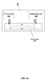
- FIG. 1A is a diagram illustrating an exemplary integrated circuit, in connection with an embodiment of the invention.
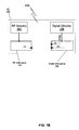
- FIG. 1B is a diagram illustrating an exemplary integrated circuit, in connection with an embodiment of the invention.
- FIG. 1C is a diagram of an exemplary integrated circuit, in accordance with an embodiment of the invention.
- FIG. 2A illustrates a cross section of an exemplary IC bonded to a package comprising a connection for mitigating the risk of an ESD event, in accordance with an embodiment of the invention.
- FIG. 2B is a diagram illustrating an ESD mitigating connection comprising a plurality of paths selectable via one or more switching elements, in accordance with an embodiment of the invention.
- FIG. 3 illustrates an exemplary layout of a path in an IC package for electrically coupling two portions of an IC to mitigate ESD risk, in accordance with an embodiment of the invention.
- FIG. 4 is a flow chart illustrating mitigation of an ESD event via a connection in an IC package, in accordance with an embodiment of the invention.
- FIG. 5 is a flow chart illustrating exemplary steps for selecting one or more paths for an ESD mitigating connection, in accordance with an embodiment of the invention.
- ESD current may be routed via one or more paths within and/or on a package to which the IC is bonded.
- the one or more paths may electrically couple two or more of the portions of the IC.
- the one or more paths may have low impedance at DC and high impedance at one or more frequencies utilized in the IC.
- One of the portions of the IC may be a ground plane for RF circuitry.
- One of the portions of the IC may be a ground plane for digital circuitry.
- the one or more paths may be selected based on the one or more frequencies utilized in the IC.
- the one or more paths may be selected based on a maximum tolerable resistance of the one or more paths.
- the maximum tolerable resistance may be determined based on a minimum voltage and/or current which the packaged integrated circuit may be expected to tolerate without damage.
- the one or more paths may be selected based on a minimum tolerable inductance of the one or more paths.
- the minimum tolerable inductance may be determined based on the one or more frequencies utilized in the integrated circuit.
- the one or more paths may comprise one or more turns.
- the one or more paths may be fabricated in one or more metal layers of the IC package.
- FIG. 1A is diagram illustrating an exemplary integrated circuit, in connection with an embodiment of the invention.
- the integrated circuit (IC) 102 may comprise an RF portion 104 and a digital portion 106 which share a ground plane 108.
- the RF portion 104 may comprise suitable logic, circuitry, and/or code that may be operable to process analog signals.
- the RF portion 104 may comprise one or more amplifiers, mixers, filters, and analog to digital converters.
- the digital portion 106 may comprise suitable logic, circuitry, and/or code that may be operable to process digital signals.
- the digital portion 106 may comprise one or more baseband processors, digital signal processors (DSP), and memory elements.
- the digital circuitry 106 may switch rapidly between at or near a negative voltage rail and at or near a positive voltage rail. This behavior may provide substantial noise margin for the digital circuitry 106, but the sharp signal transitions of the digital circuitry 106 may also generate significant amounts of noise. Consequently, the RF circuitry 104, which may be more susceptible to noise due, for example, to low signal amplitudes, may be negatively impacted by the noise from the digital circuitry 106. In this regard, noise from the digital circuitry 106 may be coupled into the RF circuitry 104 via the ground plane 108.
- FIG. 1B is a diagram illustrating an exemplary integrated circuit, in connection with an embodiment of the invention.
- the IC 122 may comprise an RF portion 104, a digital portion 106, an RF ground plane 124, and a digital ground plane 126.
- the IC 122 may be similar to the IC 102 described with respect to FIG. 1A with the difference being that the common ground 108 of the IC 102 may be replaced with separate ground planes 124 and 126 for the RF portion 104 and the digital portion 106, respectively.
- the electrical isolation between the RF ground plane 124 and the digital ground plane 126 may reduce the amount of noise coupled from the digital portion 106 to the RF portion 104.
- the electrical isolation between the RF ground plane 124 and the digital ground plane 126 may result in a voltage differential arising between separate portions of the IC 122 and/or between portions of the IC 122 and external circuits and/or objects. Accordingly, the IC 122 may be more susceptible to an ESD event than the IC 102 of FIG. 1A .
- FIG. 1C is a diagram of an exemplary integrated circuit, in accordance with an embodiment of the invention.
- an IC 142 bonded to an IC package 144.
- the IC 142 may be similar to the IC 122 described with respect to FIG. 1B , with the difference being that the RF ground plane 124 and the digital ground plane 126 in the IC 142 may be electrically coupled via an ESD risk mitigating connection 146 within and/or on the IC package 144.
- connection 146 may provide a low impedance DC path between the RF ground plane 124 and the digital ground plane 126 while simultaneously providing a high impedance AC path between the RF ground plane 124 and the digital ground plane 126.
- the low DC impedance of the connection 146 may prevent or reduce a difference in electric potential which may develop between separate portions of the IC 142 and/or between portions of the IC 142 and external circuits and/or objects.
- the high AC impedance of the connection 146 may prevent or reduce noise coupled between the RF portion 104 and the digital portion 106.
- fabricating the connection 146 in the IC package 144 may enable efficiently realizing a relatively high inductance and low resistance. In this regard, realizing the connection 146 in the IC package 144 may be less costly, in terms of space and/or dollars, than implementing the connection 146 on-chip or as an external component. Additionally, fabricating the connection 146 in the IC package 144 may enable tighter control of tolerances as compared to, for example, a discrete component. Furthermore, fabricating the connection in the IC package 144 may prevent the need to have two pins of the package 144 dedicated for coupling the RF ground plane 124 and the digital ground plane 126 externally.
- FIG. 1C depicts the connection 146 electrically coupling an RF ground 124 and a digital ground plane 126
- the connection 146 may be utilized to electrically couple any two portions of an integrated circuit between which low DC impedance and high AC impedance may be desirable.
- FIG. 2A illustrates a cross section of an exemplary IC bonded to a package comprising a connection for mitigating the risk of an ESD event, in accordance with an embodiment of the invention.
- an IC 202 comprising an RF ground plane 204 and a digital ground plane 206.
- the IC 202 may be bonded to an IC package 228 via a plurality of bond wires 208.
- the bond wires 208 may be coupled to one or more metal layers 210 of the IC package 228 by a layer of nickel plating 230 and a layer of gold plating 232.
- the various metal layers 210 may be interconnected by one or more vias 222 and/or plated through holes (PTH) 218.
- PTH plated through holes
- the IC package 228 may be communicatively coupled to one or more external components by one or more solder balls 226.
- the RF ground plane 204 and the digital ground plane 206 may be electrically coupled by an ESD mitigating connection 220 realized in one or more of the metal layers 210.
- the ESD mitigating connection 220 may comprise one or more bond wires 208, vias 222, plated through holes 218, and/or traces 224 in the metal layers 210
- the IC 202 may be similar to or the same as the IC 142 described with respect to FIG. 1C .
- the RF ground plane 204 may be similar to or the same as the RF ground plane 124 described with respect to FIGS. 1A - 1C .
- the digital ground plane 206 may be similar to or the same as the digital ground plane 126 described with respect to FIGS. 1A - 1C .
- the IC package 228 may be similar to or the same as the IC package 144 described with respect to FIG. 1C . Although, the package 228 comprises four metal layers, the invention is not so limited and any number of metal layers may be present in the IC package.
- the inductance of the connection 220 may provide noise isolation between the RF ground plane 204 and the digital ground plane 206. Fabricating the connection 220 in the IC package 228, as opposed to in the IC 202, may enable a higher inductance connection and may thus improve noise isolation between RF circuitry and digital circuitry. Additionally, placing the connection 220 in the package 228 may enable the connection 220 to be physically closer to, for example, chassis or earth ground. In this regard, in the event of an ESD event, large currents may be diverted away from the IC 202.
- the connection 220 comprises a single path from the digital GND 206 to the RF GND 294, however the invention is not so limited.
- the connection 220 may comprise a plurality of paths which may be realized in the one or more metal layers 210 of the IC package 228.
- the paths may be selected via more switching elements (not shown) in the IC 202 and/or within and/or on the package 228. Selecting different paths may enable configuring an inductance and/or resistance of the connection 220. Accordingly, the paths may be configured to adjust the inductance and/or resistance of the connection 220 based on one or more frequencies utilized by one or more circuits of the IC 202.
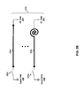
- FIG. 2B is a diagram illustrating an ESD mitigating connection comprising a plurality of paths selectable via one or more switching elements, in accordance with an embodiment of the invention.
- an ESD connection 220 comprising paths 254 1 , ..., 254 N .
- a first end of each of the paths 254 may be coupled to the digital GND 206 via a switch 252.
- a second end of each of the paths 254 may be coupled to the RF GND 206.
- Each of the paths 254 1 , ..., 254 N may comprise, for example, one or more bond wires, one or more vias in the IC or the package, one or more PTH in the IC package, and/or one or more traces in the metal layers of the IC package.
- the switches 252 1 , ..., 252 N may be configured to select one or more of the paths 254 1 , ..., 254 N .
- the inductance and/or resistance of the connection 220 may vary based on the configuration of the switches 252 1 , ..., 252 N .
- one or more of the paths 254 1 , ..., 254 N may be selected based on a mode of operation of the IC.
- one or more of the paths 254 1 , ..., 254 N may be selected based on a desired inductance and/or resistance of the connection 220.
- the paths may be configured based on a maximum tolerable resistance of the connection 220 which may provide acceptable ESD protection and/or based on a minimum tolerable inductance of the connection 220 which may provide acceptable noise isolation.
- the maximum resistance may be determined based on, for example, a minimum transient voltage and/or current which the IC 202 may be expected to withstand.
- frequencies utilized within the IC 202 may determine sensitive and/or noisy frequencies.
- FIG. 3 illustrates an exemplary layout of a path in an IC package for electrically coupling two portions of an IC to mitigate ESD risk, in accordance with an embodiment of the invention.
- the path 302 may comprise an exemplary realization of the connection 220 described with respect to FIG. 2 .
- the path 302 may be the sole path of an ESD mitigating connection or may be one or a plurality of paths of an ESD mitigating connection.
- the exemplary path 302 comprises a single trace 304, via 222a, and via 222b, the invention is not so limited.
- exemplary paths may comprise other components such as additional traces, one or more plated through holes, additional vias, and/or one or more bond wires or solder bumps.
- a size, a shape, and/or components of the path 302 may be based on desired inductance, capacitance, and/or resistance of the path 302. Additionally, the size, shape, and/or components of the path 302 may be based on available space in an IC package in which the path 302 is fabricated.
- the path 302 may comprise one or more turns to increase its inductance.
- FIG. 4 is a flow chart illustrating mitigation of an ESD event via a connection in an IC package, in accordance with an embodiment of the invention.
- the exemplary steps may begin with step 402 when a charge imbalance may develop between a packaged IC and its surroundings. Subsequent to step 402, the exemplary steps may advance to step 404.
- step 404 an electrostatic discharge may occur when the IC package touches it surroundings or when the imbalance becomes large enough to arc. The ESD may suddenly cause a large amount of current to flow between the surroundings and the IC as the charge seeks a ground path.
- the exemplary steps may advance to step 406.
- the ESD current may be routed to ground via an ESD mitigating connection fabricated in the IC package. In this manner, the ESD current may be routed to ground without traversing and/or damaging the IC.
- FIG. 5 is a flow chart illustrating exemplary steps for selecting one or more paths for an ESD mitigating connection, in accordance with an embodiment of the invention.
- the exemplary steps may begin with step 502 when one or more frequencies utilized in an IC may be measured and/or otherwise determined. Subsequent to step 502, the exemplary steps may advance to step 504. In step 504, a desired inductance and/or resistance of an ESD mitigating connection may be determined based on the frequencies determined in step 502. Subsequent to step 504, the exemplary steps may advance to step 506. In step 506, one or more switches, such as the switches 252 described with respect to FIG. 2B , may be configured to select one or more paths to achieve (within a tolerance) the inductance and/or resistance determined in step 504.
- ESD current may be routed via one or more paths 254 within and/or on a package 228 to which the IC 202 is bonded.
- the one or more paths 254 may electrically couple two or more of the portions of the IC.
- the one or more paths 254 may have low impedance at DC and high impedance at one or more frequencies utilized in the IC 202.
- One of the portions of the IC 202 may be a ground plane 204 for RF circuitry.
- One of the portions of the IC may be a ground plane 206 for digital circuitry.
- the one or more paths 254 may be selected based on the one or more frequencies utilized in the IC 202.
- the one or more paths 254 may be selected based on a maximum tolerable resistance of the one or more paths 254.
- the maximum tolerable resistance may be determined based on a minimum voltage and/or current which the packaged integrated circuit may be expected to tolerate without damage.
- the one or more paths 254 may be selected based on a minimum tolerable inductance of the one or more paths 254.
- the minimum tolerable inductance may be determined based on the one or more frequencies utilized in the integrated circuit 202.
- the one or more paths 254 may comprise one or more turns.
- the one or more paths 254 may be fabricated in one or more metal layers 210 of the package 228.
- Another embodiment of the invention may provide a machine and/or computer readable storage and/or medium, having stored thereon, a machine code and/or a computer program having at least one code section executable by a machine and/or a computer, thereby causing the machine and/or computer to perform the steps as described herein for mitigating risk of electrostatic discharge in a system on chip.
- the present invention may be realized in hardware, software, or a combination of hardware and software.
- the present invention may be realized in a centralized fashion in at least one computer system, or in a distributed fashion where different elements are spread across several interconnected computer systems. Any kind of computer system or other apparatus adapted for carrying out the methods described herein is suited.
- a typical combination of hardware and software may be a general-purpose computer system with a computer program that, when being loaded and executed, controls the computer system such that it carries out the methods described herein.
- the present invention may also be embedded in a computer program product, which comprises all the features enabling the implementation of the methods described herein, and which when loaded in a computer system is able to carry out these methods.
- Computer program in the present context means any expression, in any language, code or notation, of a set of instructions intended to cause a system having an information processing capability to perform a particular function either directly or after either or both of the following: a) conversion to another language, code or notation; b) reproduction in a different material form.
Landscapes
- Semiconductor Integrated Circuits (AREA)
Abstract
Description
- This patent application makes reference to, claims priority to and claims benefit from United States Provisional Patent Application Serial No.
61/045,666, filed on April 17, 2008 - The above stated application is hereby incorporated herein by reference in its entirety.
- Certain embodiments of the invention relate to integrated circuits. More specifically, certain embodiments of the invention relate to a method and system for mitigating risk of electrostatic discharge in a system on chip (SoC).
- Electrostatic discharge (ESD) is the rapid transfer of electric charge between two objects. ESD often results from two objects of different electric potentials being brought into sufficient proximity of one another. An ESD event can critically and irreparably damage integrated circuits. For example, an ESD event may result in dielectric breakdown and/or fusing in one or more circuit elements, often resulting in permanently shorted and/or permanently open circuits.
- Further limitations and disadvantages of conventional and traditional approaches will become apparent to one of skill in the art, through comparison of such systems with some aspects of the present invention as set forth in the remainder of the present application with reference to the drawings.
- A system and/or method is provided mitigating risk of electrostatic discharge in a system on chip (SoC), substantially as shown in and/or described in connection with at least one of the figures, as set forth more completely in the claims.
According to an aspect, a method for controlling electrostatic discharge is provided, the method comprising: - for an integrated circuit comprising a plurality of portions electrically isolated from one another within said integrated circuit:
- routing ESD current via one or more paths within and/or on a package to which said integrated circuit is bonded, wherein said one or more paths:
- electrically couple two or more of said plurality of portions; and
- are characterized by low impedance at DC and high impedance at one or more frequencies utilized by circuits within said integrated circuit.
- routing ESD current via one or more paths within and/or on a package to which said integrated circuit is bonded, wherein said one or more paths:
- Advantageously, one of said plurality of portions is a ground plane for RF circuitry within said integrated circuit.
- Advantageously, one of said plurality of portions is a ground plane for digital circuitry within said integrated circuit.
- Advantageously, the method further comprises selecting said one or more paths via one or more switching elements based on said one or more frequencies utilized in said integrated circuit.
- Advantageously, the method further comprises selecting said one or more paths via one or more switching elements based on a maximum tolerable resistance of said one or more paths.
- Advantageously, the method further comprises determining said maximum tolerable resistance based on a minimum voltage and/or current which the packaged integrated circuit is expected to tolerate without damage.
- Advantageously, the method further comprises selecting said one or more paths via one or more switching elements based on a minimum tolerable inductance of said one or more paths.
- Advantageously, the method further comprises determining said minimum tolerable inductance based on said one or more frequencies utilized in said integrated circuit.
- Advantageously, said one or more paths comprise one or more turns.
- Advantageously, said one or more paths are fabricated in one or more metal layers of said package.
- According to an aspect, a system for controlling electrostatic discharge is provided, the system comprising:
- one or more paths within and/or on an integrated circuit package bonded to an integrated circuit, said integrated circuit comprising a plurality of portions electrically isolated from one another within said integrated circuit, wherein said one or more paths:
- route ESD current;
- electrically couple two or more of said plurality of portions; and
- are characterized by low impedance at DC and high impedance at one or more frequencies utilized by circuits within said integrated circuit.
- one or more paths within and/or on an integrated circuit package bonded to an integrated circuit, said integrated circuit comprising a plurality of portions electrically isolated from one another within said integrated circuit, wherein said one or more paths:
- Advantageously, a first of said plurality of portions is a ground plane for RF circuitry of said integrated circuit.
- Advantageously, a second of said plurality of portions is a ground plane for digital circuitry of said integrated circuit.
- Advantageously, a size, shape, and/or number of said one or more paths is based on a frequency of operation of one or more portions of said integrated circuit.
- Advantageously, a size, shape, and/or number of said one or more paths is based on a maximum tolerable resistance of said one or more paths.
- Advantageously, said maximum tolerable resistance is based on a minimum voltage and/or current which the packaged integrated circuit is expected to tolerate without damage.
- Advantageously, a size, shape, and/or number of said one or more paths is based on a minimum tolerable inductance of said one or more paths.
- Advantageously, said minimum tolerable inductance is based on frequencies utilized in said integrated circuit.
- Advantageously, said one or more paths comprise one or more turns.
- Advantageously, said one or more paths are fabricated in one or more metal layers of said integrated circuit package.
- These and other advantages, aspects and novel features of the present invention, as well as details of an illustrated embodiment thereof, will be more fully understood from the following description and drawings.
-
FIG. 1A is a diagram illustrating an exemplary integrated circuit, in connection with an embodiment of the invention. -
FIG. 1B is a diagram illustrating an exemplary integrated circuit, in connection with an embodiment of the invention. -
FIG. 1C is a diagram of an exemplary integrated circuit, in accordance with an embodiment of the invention. -
FIG. 2A illustrates a cross section of an exemplary IC bonded to a package comprising a connection for mitigating the risk of an ESD event, in accordance with an embodiment of the invention. -
FIG. 2B is a diagram illustrating an ESD mitigating connection comprising a plurality of paths selectable via one or more switching elements, in accordance with an embodiment of the invention. -
FIG. 3 illustrates an exemplary layout of a path in an IC package for electrically coupling two portions of an IC to mitigate ESD risk, in accordance with an embodiment of the invention. -
FIG. 4 is a flow chart illustrating mitigation of an ESD event via a connection in an IC package, in accordance with an embodiment of the invention. -
FIG. 5 is a flow chart illustrating exemplary steps for selecting one or more paths for an ESD mitigating connection, in accordance with an embodiment of the invention. - Certain embodiments of the invention may be found in a method and system for mitigating risk of electrostatic discharge in a system on chip (SoC). In various exemplary embodiments of the invention, for an IC comprising a plurality of portions electrically isolated from one another within the IC, ESD current may be routed via one or more paths within and/or on a package to which the IC is bonded. The one or more paths may electrically couple two or more of the portions of the IC. The one or more paths may have low impedance at DC and high impedance at one or more frequencies utilized in the IC. One of the portions of the IC may be a ground plane for RF circuitry. One of the portions of the IC may be a ground plane for digital circuitry. The one or more paths may be selected based on the one or more frequencies utilized in the IC. The one or more paths may be selected based on a maximum tolerable resistance of the one or more paths. The maximum tolerable resistance may be determined based on a minimum voltage and/or current which the packaged integrated circuit may be expected to tolerate without damage. The one or more paths may be selected based on a minimum tolerable inductance of the one or more paths. The minimum tolerable inductance may be determined based on the one or more frequencies utilized in the integrated circuit. The one or more paths may comprise one or more turns. The one or more paths may be fabricated in one or more metal layers of the IC package.
-
FIG. 1A is diagram illustrating an exemplary integrated circuit, in connection with an embodiment of the invention. Referring toFIG. 1A , the integrated circuit (IC) 102 may comprise anRF portion 104 and adigital portion 106 which share aground plane 108. - The
RF portion 104 may comprise suitable logic, circuitry, and/or code that may be operable to process analog signals. In various exemplary embodiments of the invention, theRF portion 104 may comprise one or more amplifiers, mixers, filters, and analog to digital converters. - The
digital portion 106 may comprise suitable logic, circuitry, and/or code that may be operable to process digital signals. In various exemplary embodiments of the invention, thedigital portion 106 may comprise one or more baseband processors, digital signal processors (DSP), and memory elements. - In operation, the
digital circuitry 106 may switch rapidly between at or near a negative voltage rail and at or near a positive voltage rail. This behavior may provide substantial noise margin for thedigital circuitry 106, but the sharp signal transitions of thedigital circuitry 106 may also generate significant amounts of noise. Consequently, theRF circuitry 104, which may be more susceptible to noise due, for example, to low signal amplitudes, may be negatively impacted by the noise from thedigital circuitry 106. In this regard, noise from thedigital circuitry 106 may be coupled into theRF circuitry 104 via theground plane 108. -
FIG. 1B is a diagram illustrating an exemplary integrated circuit, in connection with an embodiment of the invention. Referring toFIG. 1B , the IC 122 may comprise anRF portion 104, adigital portion 106, anRF ground plane 124, and adigital ground plane 126. - The IC 122 may be similar to the IC 102 described with respect to
FIG. 1A with the difference being that thecommon ground 108 of the IC 102 may be replaced withseparate ground planes RF portion 104 and thedigital portion 106, respectively. - In operation, the electrical isolation between the
RF ground plane 124 and thedigital ground plane 126 may reduce the amount of noise coupled from thedigital portion 106 to theRF portion 104. However, the electrical isolation between theRF ground plane 124 and thedigital ground plane 126 may result in a voltage differential arising between separate portions of the IC 122 and/or between portions of the IC 122 and external circuits and/or objects. Accordingly, the IC 122 may be more susceptible to an ESD event than the IC 102 ofFIG. 1A . -
FIG. 1C is a diagram of an exemplary integrated circuit, in accordance with an embodiment of the invention. Referring toFIG 1C , there is shown anIC 142, bonded to an IC package 144. TheIC 142 may be similar to the IC 122 described with respect toFIG. 1B , with the difference being that theRF ground plane 124 and thedigital ground plane 126 in theIC 142 may be electrically coupled via an ESDrisk mitigating connection 146 within and/or on the IC package 144. - In operation, the
connection 146 may provide a low impedance DC path between theRF ground plane 124 and thedigital ground plane 126 while simultaneously providing a high impedance AC path between theRF ground plane 124 and thedigital ground plane 126. The low DC impedance of theconnection 146 may prevent or reduce a difference in electric potential which may develop between separate portions of theIC 142 and/or between portions of theIC 142 and external circuits and/or objects. The high AC impedance of theconnection 146 may prevent or reduce noise coupled between theRF portion 104 and thedigital portion 106. - Fabricating the
connection 146 in the IC package 144 may enable efficiently realizing a relatively high inductance and low resistance. In this regard, realizing theconnection 146 in the IC package 144 may be less costly, in terms of space and/or dollars, than implementing theconnection 146 on-chip or as an external component. Additionally, fabricating theconnection 146 in the IC package 144 may enable tighter control of tolerances as compared to, for example, a discrete component. Furthermore, fabricating the connection in the IC package 144 may prevent the need to have two pins of the package 144 dedicated for coupling theRF ground plane 124 and thedigital ground plane 126 externally. - Although
FIG. 1C depicts theconnection 146 electrically coupling anRF ground 124 and adigital ground plane 126, the invention is not so limited. In this regard, theconnection 146 may be utilized to electrically couple any two portions of an integrated circuit between which low DC impedance and high AC impedance may be desirable. -
FIG. 2A illustrates a cross section of an exemplary IC bonded to a package comprising a connection for mitigating the risk of an ESD event, in accordance with an embodiment of the invention. Referring toFIG. 2A there is shown anIC 202 comprising anRF ground plane 204 and adigital ground plane 206. TheIC 202 may be bonded to anIC package 228 via a plurality ofbond wires 208. Thebond wires 208 may be coupled to one ormore metal layers 210 of theIC package 228 by a layer of nickel plating 230 and a layer ofgold plating 232. Thevarious metal layers 210 may be interconnected by one ormore vias 222 and/or plated through holes (PTH) 218. TheIC package 228 may be communicatively coupled to one or more external components by one ormore solder balls 226. TheRF ground plane 204 and thedigital ground plane 206 may be electrically coupled by anESD mitigating connection 220 realized in one or more of the metal layers 210. TheESD mitigating connection 220 may comprise one ormore bond wires 208, vias 222, plated throughholes 218, and/or traces 224 in the metal layers 210 - The
IC 202 may be similar to or the same as theIC 142 described with respect toFIG. 1C . TheRF ground plane 204 may be similar to or the same as theRF ground plane 124 described with respect toFIGS. 1A - 1C . Thedigital ground plane 206 may be similar to or the same as thedigital ground plane 126 described with respect toFIGS. 1A - 1C . TheIC package 228 may be similar to or the same as the IC package 144 described with respect toFIG. 1C . Although, thepackage 228 comprises four metal layers, the invention is not so limited and any number of metal layers may be present in the IC package. - In operation, the inductance of the
connection 220 may provide noise isolation between theRF ground plane 204 and thedigital ground plane 206. Fabricating theconnection 220 in theIC package 228, as opposed to in theIC 202, may enable a higher inductance connection and may thus improve noise isolation between RF circuitry and digital circuitry. Additionally, placing theconnection 220 in thepackage 228 may enable theconnection 220 to be physically closer to, for example, chassis or earth ground. In this regard, in the event of an ESD event, large currents may be diverted away from theIC 202. - In the exemplary embodiment of the invention depicted in
FIG. 2A , theconnection 220 comprises a single path from thedigital GND 206 to the RF GND 294, however the invention is not so limited. In this regard, theconnection 220 may comprise a plurality of paths which may be realized in the one ormore metal layers 210 of theIC package 228. Additionally, in various embodiments of the invention, the paths may be selected via more switching elements (not shown) in theIC 202 and/or within and/or on thepackage 228. Selecting different paths may enable configuring an inductance and/or resistance of theconnection 220. Accordingly, the paths may be configured to adjust the inductance and/or resistance of theconnection 220 based on one or more frequencies utilized by one or more circuits of theIC 202. -
FIG. 2B is a diagram illustrating an ESD mitigating connection comprising a plurality of paths selectable via one or more switching elements, in accordance with an embodiment of the invention. Referring toFIG. 2B there is shown anESD connection 220 comprisingpaths 2541, ..., 254N. A first end of each of thepaths 254 may be coupled to thedigital GND 206 via a switch 252. A second end of each of thepaths 254 may be coupled to theRF GND 206. Each of thepaths 2541, ..., 254N may comprise, for example, one or more bond wires, one or more vias in the IC or the package, one or more PTH in the IC package, and/or one or more traces in the metal layers of the IC package. - In operation, the switches 2521, ..., 252N may be configured to select one or more of the
paths 2541, ..., 254N. In this regard, the inductance and/or resistance of theconnection 220 may vary based on the configuration of the switches 2521, ..., 252N. In various exemplary embodiments of the invention, one or more of thepaths 2541, ..., 254N may be selected based on a mode of operation of the IC. In various exemplary embodiments of the invention, one or more of thepaths 2541, ..., 254N may be selected based on a desired inductance and/or resistance of theconnection 220. For example, the paths may be configured based on a maximum tolerable resistance of theconnection 220 which may provide acceptable ESD protection and/or based on a minimum tolerable inductance of theconnection 220 which may provide acceptable noise isolation. In regards to ESD, the maximum resistance may be determined based on, for example, a minimum transient voltage and/or current which theIC 202 may be expected to withstand. In regards to noise, frequencies utilized within theIC 202 may determine sensitive and/or noisy frequencies. -
FIG. 3 illustrates an exemplary layout of a path in an IC package for electrically coupling two portions of an IC to mitigate ESD risk, in accordance with an embodiment of the invention. Referring toFIG. 3 , thepath 302 may comprise an exemplary realization of theconnection 220 described with respect toFIG. 2 . In various embodiments of the invention, thepath 302 may be the sole path of an ESD mitigating connection or may be one or a plurality of paths of an ESD mitigating connection. Although theexemplary path 302 comprises asingle trace 304, via 222a, and via 222b, the invention is not so limited. For example, other exemplary paths may comprise other components such as additional traces, one or more plated through holes, additional vias, and/or one or more bond wires or solder bumps. In this regard, a size, a shape, and/or components of thepath 302 may be based on desired inductance, capacitance, and/or resistance of thepath 302. Additionally, the size, shape, and/or components of thepath 302 may be based on available space in an IC package in which thepath 302 is fabricated. In various embodiments of the invention, thepath 302 may comprise one or more turns to increase its inductance. -
FIG. 4 is a flow chart illustrating mitigation of an ESD event via a connection in an IC package, in accordance with an embodiment of the invention. Referring toFIG. 4 , the exemplary steps may begin withstep 402 when a charge imbalance may develop between a packaged IC and its surroundings. Subsequent to step 402, the exemplary steps may advance to step 404. Instep 404, an electrostatic discharge may occur when the IC package touches it surroundings or when the imbalance becomes large enough to arc. The ESD may suddenly cause a large amount of current to flow between the surroundings and the IC as the charge seeks a ground path. Subsequent to step 404, the exemplary steps may advance to step 406. Instep 406, the ESD current may be routed to ground via an ESD mitigating connection fabricated in the IC package. In this manner, the ESD current may be routed to ground without traversing and/or damaging the IC. -
FIG. 5 is a flow chart illustrating exemplary steps for selecting one or more paths for an ESD mitigating connection, in accordance with an embodiment of the invention. Referring toFIG. 5 , the exemplary steps may begin withstep 502 when one or more frequencies utilized in an IC may be measured and/or otherwise determined. Subsequent to step 502, the exemplary steps may advance to step 504. Instep 504, a desired inductance and/or resistance of an ESD mitigating connection may be determined based on the frequencies determined instep 502. Subsequent to step 504, the exemplary steps may advance to step 506. Instep 506, one or more switches, such as the switches 252 described with respect toFIG. 2B , may be configured to select one or more paths to achieve (within a tolerance) the inductance and/or resistance determined instep 504. - Exemplary aspects of a method and system for mitigating risk of electrostatic discharge in a system on chip are provided. In an exemplary embodiment of the invention, for an
IC 202 comprising a plurality of portions electrically isolated from one another within the IC, ESD current may be routed via one ormore paths 254 within and/or on apackage 228 to which theIC 202 is bonded. The one ormore paths 254 may electrically couple two or more of the portions of the IC. The one ormore paths 254 may have low impedance at DC and high impedance at one or more frequencies utilized in theIC 202. One of the portions of theIC 202 may be aground plane 204 for RF circuitry. One of the portions of the IC may be aground plane 206 for digital circuitry. The one ormore paths 254 may be selected based on the one or more frequencies utilized in theIC 202. The one ormore paths 254 may be selected based on a maximum tolerable resistance of the one ormore paths 254. The maximum tolerable resistance may be determined based on a minimum voltage and/or current which the packaged integrated circuit may be expected to tolerate without damage. The one ormore paths 254 may be selected based on a minimum tolerable inductance of the one ormore paths 254. The minimum tolerable inductance may be determined based on the one or more frequencies utilized in theintegrated circuit 202. The one ormore paths 254 may comprise one or more turns. The one ormore paths 254 may be fabricated in one ormore metal layers 210 of thepackage 228. - Another embodiment of the invention may provide a machine and/or computer readable storage and/or medium, having stored thereon, a machine code and/or a computer program having at least one code section executable by a machine and/or a computer, thereby causing the machine and/or computer to perform the steps as described herein for mitigating risk of electrostatic discharge in a system on chip.
- Accordingly, the present invention may be realized in hardware, software, or a combination of hardware and software. The present invention may be realized in a centralized fashion in at least one computer system, or in a distributed fashion where different elements are spread across several interconnected computer systems. Any kind of computer system or other apparatus adapted for carrying out the methods described herein is suited. A typical combination of hardware and software may be a general-purpose computer system with a computer program that, when being loaded and executed, controls the computer system such that it carries out the methods described herein.
- The present invention may also be embedded in a computer program product, which comprises all the features enabling the implementation of the methods described herein, and which when loaded in a computer system is able to carry out these methods. Computer program in the present context means any expression, in any language, code or notation, of a set of instructions intended to cause a system having an information processing capability to perform a particular function either directly or after either or both of the following: a) conversion to another language, code or notation; b) reproduction in a different material form.
- While the present invention has been described with reference to certain embodiments, it will be understood by those skilled in the art that various changes may be made and equivalents may be substituted without departing from the scope of the present invention. In addition, many modifications may be made to adapt a particular situation or material to the teachings of the present invention without departing from its scope. Therefore, it is intended that the present invention not be limited to the particular embodiment disclosed, but that the present invention will include all embodiments falling within the scope of the appended claims.
Claims (10)
- A method for controlling electrostatic discharge, the method comprising:for an integrated circuit comprising a plurality of portions electrically isolated from one another within said integrated circuit:routing ESD current via one or more paths within and/or on a package to which said integrated circuit is bonded, wherein said one or more paths:electrically couple two or more of said plurality of portions; andare characterized by low impedance at DC and high impedance at one or more frequencies utilized by circuits within said integrated circuit.
- The method according to claim 1, wherein one of said plurality of portions is a ground plane for RF circuitry within said integrated circuit.
- The method according to claim 1, wherein one of said plurality of portions is a ground plane for digital circuitry within said integrated circuit.
- The method according to claim 1, comprising selecting said one or more paths via one or more switching elements based on said one or more frequencies utilized in said integrated circuit.
- The method according to claim 1, comprising selecting said one or more paths via one or more switching elements based on a maximum tolerable resistance of said one or more paths.
- The method according to claim 5, comprising determining said maximum tolerable resistance based on a minimum voltage and/or current which the packaged integrated circuit is expected to tolerate without damage.
- A system for controlling electrostatic discharge, the system comprising:one or more paths within and/or on an integrated circuit package bonded to an integrated circuit, said integrated circuit comprising a plurality of portions electrically isolated from one another within said integrated circuit, wherein said one or more paths:route ESD current;electrically couple two or more of said plurality of portions; andare characterized by low impedance at DC and high impedance at one or more frequencies utilized by circuits within said integrated circuit.
- The system according to claim 7, wherein a first of said plurality of portions is a ground plane for RF circuitry of said integrated circuit.
- The system according to claim 7, wherein a second of said plurality of portions is a ground plane for digital circuitry of said integrated circuit.
- The system according to claim 7, wherein a size, shape, and/or number of said one or more paths is based on a frequency of operation of one or more portions of said integrated circuit.
Applications Claiming Priority (2)
| Application Number | Priority Date | Filing Date | Title |
|---|---|---|---|
| US4566608P | 2008-04-17 | 2008-04-17 | |
| US12/265,601 US8077439B2 (en) | 2008-04-17 | 2008-11-05 | Method and system for mitigating risk of electrostatic discharge for a system on chip (SOC) |
Publications (3)
| Publication Number | Publication Date |
|---|---|
| EP2110852A2 true EP2110852A2 (en) | 2009-10-21 |
| EP2110852A3 EP2110852A3 (en) | 2014-03-05 |
| EP2110852B1 EP2110852B1 (en) | 2019-06-12 |
Family
ID=40848662
Family Applications (1)
| Application Number | Title | Priority Date | Filing Date |
|---|---|---|---|
| EP09004871.1A Active EP2110852B1 (en) | 2008-04-17 | 2009-04-01 | Method and system for mitigating risk of electrostatic discharge for a system on chip (SoC) |
Country Status (2)
| Country | Link |
|---|---|
| US (1) | US8077439B2 (en) |
| EP (1) | EP2110852B1 (en) |
Cited By (1)
| Publication number | Priority date | Publication date | Assignee | Title |
|---|---|---|---|---|
| EP3457435A1 (en) * | 2017-09-14 | 2019-03-20 | Nxp B.V. | Electrostatic discharge protection structure |
Families Citing this family (4)
| Publication number | Priority date | Publication date | Assignee | Title |
|---|---|---|---|---|
| US10015916B1 (en) * | 2013-05-21 | 2018-07-03 | Xilinx, Inc. | Removal of electrostatic charges from an interposer via a ground pad thereof for die attach for formation of a stacked die |
| US9960227B2 (en) | 2013-09-11 | 2018-05-01 | Xilinx, Inc. | Removal of electrostatic charges from interposer for die attachment |
| JP6293562B2 (en) * | 2014-04-17 | 2018-03-14 | 株式会社不二工機 | Pressure sensor |
| US11227834B2 (en) * | 2020-01-29 | 2022-01-18 | Seagate Technology Llc | Package grounding system |
Family Cites Families (16)
| Publication number | Priority date | Publication date | Assignee | Title |
|---|---|---|---|---|
| US3934136A (en) * | 1974-05-06 | 1976-01-20 | Minnesota Mining And Manufacturing Company | Threshold signal circuitry for scanning apparatus |
| TW289153B (en) * | 1994-09-26 | 1996-10-21 | Ibm | |
| US5835327A (en) * | 1996-11-25 | 1998-11-10 | Advanced Micro Devices, Inc. | ESD protection continuous monitoring device |
| US6740821B1 (en) * | 2002-03-01 | 2004-05-25 | Micron Technology, Inc. | Selectively configurable circuit board |
| US6934136B2 (en) * | 2002-04-24 | 2005-08-23 | Texas Instrument Incorporated | ESD protection of noise decoupling capacitors |
| JP3713013B2 (en) * | 2002-12-06 | 2005-11-02 | 松下電器産業株式会社 | Manufacturing method of semiconductor integrated circuit device |
| FR2856196B1 (en) * | 2003-06-13 | 2005-09-09 | St Microelectronics Sa | ELECTRONIC COMPONENT PROTECTING ELECTROSTATIC DISCHARGES |
| US7522394B2 (en) * | 2003-08-21 | 2009-04-21 | Broadcom Corporation | Radio frequency integrated circuit having sectional ESD protection |
| KR100725361B1 (en) * | 2005-02-24 | 2007-06-07 | 삼성전자주식회사 | Multi-power block type integrated circuit device with ESD protection element and power clamp |
| DE102005014176B4 (en) * | 2005-03-29 | 2009-08-20 | Infineon Technologies Ag | Method for creating a protective arrangement for protecting an electronic module from electrostatic discharges and appropriately designed electronic module |
| US20070178766A1 (en) * | 2006-01-31 | 2007-08-02 | Intel Corporation | Passive impedance equalization of high speed serial links |
| KR100713935B1 (en) * | 2006-04-14 | 2007-05-07 | 주식회사 하이닉스반도체 | Electrostatic Discharge Protection Circuit and Electrostatic Discharge Protection Method of Semiconductor Memory Device |
| US7894205B2 (en) * | 2007-04-05 | 2011-02-22 | Mitsubishi Electric Corporation | Variable device circuit and method for manufacturing the same |
| US20090080135A1 (en) * | 2007-09-21 | 2009-03-26 | Broadcom Corporation | Apparatus and Method for ESD Protection of an Integrated Circuit |
| US7858402B2 (en) * | 2007-11-28 | 2010-12-28 | Broadcom Corporation | Integrated circuit package having reversible ESD protection |
| CN101453066A (en) * | 2007-12-04 | 2009-06-10 | 鸿富锦精密工业(深圳)有限公司 | Switching board |
-
2008
- 2008-11-05 US US12/265,601 patent/US8077439B2/en not_active Expired - Fee Related
-
2009
- 2009-04-01 EP EP09004871.1A patent/EP2110852B1/en active Active
Cited By (3)
| Publication number | Priority date | Publication date | Assignee | Title |
|---|---|---|---|---|
| EP3457435A1 (en) * | 2017-09-14 | 2019-03-20 | Nxp B.V. | Electrostatic discharge protection structure |
| CN109509748A (en) * | 2017-09-14 | 2019-03-22 | 恩智浦有限公司 | ESD-protection structure |
| CN109509748B (en) * | 2017-09-14 | 2024-05-28 | 恩智浦有限公司 | Electrostatic discharge protection structure |
Also Published As
| Publication number | Publication date |
|---|---|
| US8077439B2 (en) | 2011-12-13 |
| EP2110852A3 (en) | 2014-03-05 |
| US20090262475A1 (en) | 2009-10-22 |
| EP2110852B1 (en) | 2019-06-12 |
Similar Documents
| Publication | Publication Date | Title |
|---|---|---|
| US8174843B2 (en) | Printed circuit board | |
| US10756032B2 (en) | Seal ring inductor and method of forming the same | |
| US7594105B2 (en) | Multilayer print circuit board | |
| US9230926B2 (en) | Functionalised redistribution layer | |
| US20140225700A1 (en) | Substrate-less discrete coupled inductor structure | |
| US8077439B2 (en) | Method and system for mitigating risk of electrostatic discharge for a system on chip (SOC) | |
| US20090213526A1 (en) | Capacitor devices with co-coupling electrode planes | |
| JP2017011081A (en) | Power semiconductor module and power converter using the same | |
| JP2009055019A (en) | Multilayer substrate, package substrate for semiconductor integrated circuit, and printed wiring board for mounting semiconductor integrated circuit | |
| JP2011014719A (en) | Semiconductor device | |
| US7375978B2 (en) | Method and apparatus for trace shielding and routing on a substrate | |
| US20190214276A1 (en) | Multi-voltage apparatus for electronics package including magnetic inductor & capacitor and manufacturing thereof | |
| US8786071B2 (en) | Wiring pattern having a stub wire | |
| US20120188729A1 (en) | Printed circuit board and manufacturing method thereof | |
| JP2007048879A (en) | Electronic equipment | |
| US11605602B2 (en) | Apparatus, system, and method for increased current distribution on high-density circuit boards | |
| CN112582379B (en) | Patterned shielding structure | |
| CN112055960B (en) | Terminal camera protection circuit | |
| JPWO2016092833A1 (en) | Electronic circuit and electronic circuit mounting method | |
| US7956493B2 (en) | Integrated circuit and method for manufacturing an integrated circuit | |
| US7821118B1 (en) | Power distribution pattern for a ball grid array | |
| JP2006310713A (en) | Printed wiring board | |
| JP2018125336A (en) | Semiconductor chip | |
| JP2006120786A (en) | Printed wiring board and electronic device |
Legal Events
| Date | Code | Title | Description |
|---|---|---|---|
| PUAI | Public reference made under article 153(3) epc to a published international application that has entered the european phase |
Free format text: ORIGINAL CODE: 0009012 |
|
| AK | Designated contracting states |
Kind code of ref document: A2 Designated state(s): AT BE BG CH CY CZ DE DK EE ES FI FR GB GR HR HU IE IS IT LI LT LU LV MC MK MT NL NO PL PT RO SE SI SK TR |
|
| RIN1 | Information on inventor provided before grant (corrected) |
Inventor name: SZE, MING WANG Inventor name: OERTLE, KENT Inventor name: DARABI, HOOMAN Inventor name: CHANG, PAUL |
|
| PUAL | Search report despatched |
Free format text: ORIGINAL CODE: 0009013 |
|
| AK | Designated contracting states |
Kind code of ref document: A3 Designated state(s): AT BE BG CH CY CZ DE DK EE ES FI FR GB GR HR HU IE IS IT LI LT LU LV MC MK MT NL NO PL PT RO SE SI SK TR |
|
| AX | Request for extension of the european patent |
Extension state: AL BA RS |
|
| RIC1 | Information provided on ipc code assigned before grant |
Ipc: H01L 23/60 20060101AFI20140130BHEP |
|
| 17P | Request for examination filed |
Effective date: 20140905 |
|
| RBV | Designated contracting states (corrected) |
Designated state(s): AT BE BG CH CY CZ DE DK EE ES FI FR GB GR HR HU IE IS IT LI LT LU LV MC MK MT NL NO PL PT RO SE SI SK TR |
|
| RAP1 | Party data changed (applicant data changed or rights of an application transferred) |
Owner name: AVAGO TECHNOLOGIES GENERAL IP (SINGAPORE) PTE. LTD |
|
| STAA | Information on the status of an ep patent application or granted ep patent |
Free format text: STATUS: EXAMINATION IS IN PROGRESS |
|
| 17Q | First examination report despatched |
Effective date: 20180619 |
|
| RIC1 | Information provided on ipc code assigned before grant |
Ipc: H01L 23/60 20060101AFI20180817BHEP |
|
| GRAP | Despatch of communication of intention to grant a patent |
Free format text: ORIGINAL CODE: EPIDOSNIGR1 |
|
| STAA | Information on the status of an ep patent application or granted ep patent |
Free format text: STATUS: GRANT OF PATENT IS INTENDED |
|
| RAP1 | Party data changed (applicant data changed or rights of an application transferred) |
Owner name: AVAGO TECHNOLOGIES INTERNATIONAL SALES PTE. LIMITE |
|
| INTG | Intention to grant announced |
Effective date: 20181204 |
|
| GRAS | Grant fee paid |
Free format text: ORIGINAL CODE: EPIDOSNIGR3 |
|
| GRAA | (expected) grant |
Free format text: ORIGINAL CODE: 0009210 |
|
| STAA | Information on the status of an ep patent application or granted ep patent |
Free format text: STATUS: THE PATENT HAS BEEN GRANTED |
|
| AK | Designated contracting states |
Kind code of ref document: B1 Designated state(s): AT BE BG CH CY CZ DE DK EE ES FI FR GB GR HR HU IE IS IT LI LT LU LV MC MK MT NL NO PL PT RO SE SI SK TR |
|
| REG | Reference to a national code |
Ref country code: GB Ref legal event code: FG4D |
|
| REG | Reference to a national code |
Ref country code: CH Ref legal event code: EP |
|
| REG | Reference to a national code |
Ref country code: AT Ref legal event code: REF Ref document number: 1143694 Country of ref document: AT Kind code of ref document: T Effective date: 20190615 |
|
| REG | Reference to a national code |
Ref country code: DE Ref legal event code: R096 Ref document number: 602009058678 Country of ref document: DE |
|
| REG | Reference to a national code |
Ref country code: IE Ref legal event code: FG4D |
|
| REG | Reference to a national code |
Ref country code: NL Ref legal event code: MP Effective date: 20190612 |
|
| REG | Reference to a national code |
Ref country code: LT Ref legal event code: MG4D |
|
| PG25 | Lapsed in a contracting state [announced via postgrant information from national office to epo] |
Ref country code: NO Free format text: LAPSE BECAUSE OF FAILURE TO SUBMIT A TRANSLATION OF THE DESCRIPTION OR TO PAY THE FEE WITHIN THE PRESCRIBED TIME-LIMIT Effective date: 20190912 Ref country code: FI Free format text: LAPSE BECAUSE OF FAILURE TO SUBMIT A TRANSLATION OF THE DESCRIPTION OR TO PAY THE FEE WITHIN THE PRESCRIBED TIME-LIMIT Effective date: 20190612 Ref country code: SE Free format text: LAPSE BECAUSE OF FAILURE TO SUBMIT A TRANSLATION OF THE DESCRIPTION OR TO PAY THE FEE WITHIN THE PRESCRIBED TIME-LIMIT Effective date: 20190612 Ref country code: HR Free format text: LAPSE BECAUSE OF FAILURE TO SUBMIT A TRANSLATION OF THE DESCRIPTION OR TO PAY THE FEE WITHIN THE PRESCRIBED TIME-LIMIT Effective date: 20190612 Ref country code: ES Free format text: LAPSE BECAUSE OF FAILURE TO SUBMIT A TRANSLATION OF THE DESCRIPTION OR TO PAY THE FEE WITHIN THE PRESCRIBED TIME-LIMIT Effective date: 20190612 Ref country code: LT Free format text: LAPSE BECAUSE OF FAILURE TO SUBMIT A TRANSLATION OF THE DESCRIPTION OR TO PAY THE FEE WITHIN THE PRESCRIBED TIME-LIMIT Effective date: 20190612 |
|
| PG25 | Lapsed in a contracting state [announced via postgrant information from national office to epo] |
Ref country code: GR Free format text: LAPSE BECAUSE OF FAILURE TO SUBMIT A TRANSLATION OF THE DESCRIPTION OR TO PAY THE FEE WITHIN THE PRESCRIBED TIME-LIMIT Effective date: 20190913 Ref country code: BG Free format text: LAPSE BECAUSE OF FAILURE TO SUBMIT A TRANSLATION OF THE DESCRIPTION OR TO PAY THE FEE WITHIN THE PRESCRIBED TIME-LIMIT Effective date: 20190912 Ref country code: LV Free format text: LAPSE BECAUSE OF FAILURE TO SUBMIT A TRANSLATION OF THE DESCRIPTION OR TO PAY THE FEE WITHIN THE PRESCRIBED TIME-LIMIT Effective date: 20190612 |
|
| REG | Reference to a national code |
Ref country code: AT Ref legal event code: MK05 Ref document number: 1143694 Country of ref document: AT Kind code of ref document: T Effective date: 20190612 |
|
| PG25 | Lapsed in a contracting state [announced via postgrant information from national office to epo] |
Ref country code: RO Free format text: LAPSE BECAUSE OF FAILURE TO SUBMIT A TRANSLATION OF THE DESCRIPTION OR TO PAY THE FEE WITHIN THE PRESCRIBED TIME-LIMIT Effective date: 20190612 Ref country code: CZ Free format text: LAPSE BECAUSE OF FAILURE TO SUBMIT A TRANSLATION OF THE DESCRIPTION OR TO PAY THE FEE WITHIN THE PRESCRIBED TIME-LIMIT Effective date: 20190612 Ref country code: EE Free format text: LAPSE BECAUSE OF FAILURE TO SUBMIT A TRANSLATION OF THE DESCRIPTION OR TO PAY THE FEE WITHIN THE PRESCRIBED TIME-LIMIT Effective date: 20190612 Ref country code: AT Free format text: LAPSE BECAUSE OF FAILURE TO SUBMIT A TRANSLATION OF THE DESCRIPTION OR TO PAY THE FEE WITHIN THE PRESCRIBED TIME-LIMIT Effective date: 20190612 Ref country code: NL Free format text: LAPSE BECAUSE OF FAILURE TO SUBMIT A TRANSLATION OF THE DESCRIPTION OR TO PAY THE FEE WITHIN THE PRESCRIBED TIME-LIMIT Effective date: 20190612 Ref country code: SK Free format text: LAPSE BECAUSE OF FAILURE TO SUBMIT A TRANSLATION OF THE DESCRIPTION OR TO PAY THE FEE WITHIN THE PRESCRIBED TIME-LIMIT Effective date: 20190612 Ref country code: PT Free format text: LAPSE BECAUSE OF FAILURE TO SUBMIT A TRANSLATION OF THE DESCRIPTION OR TO PAY THE FEE WITHIN THE PRESCRIBED TIME-LIMIT Effective date: 20191014 |
|
| PG25 | Lapsed in a contracting state [announced via postgrant information from national office to epo] |
Ref country code: IT Free format text: LAPSE BECAUSE OF FAILURE TO SUBMIT A TRANSLATION OF THE DESCRIPTION OR TO PAY THE FEE WITHIN THE PRESCRIBED TIME-LIMIT Effective date: 20190612 Ref country code: IS Free format text: LAPSE BECAUSE OF FAILURE TO SUBMIT A TRANSLATION OF THE DESCRIPTION OR TO PAY THE FEE WITHIN THE PRESCRIBED TIME-LIMIT Effective date: 20191012 |
|
| REG | Reference to a national code |
Ref country code: DE Ref legal event code: R097 Ref document number: 602009058678 Country of ref document: DE |
|
| PG25 | Lapsed in a contracting state [announced via postgrant information from national office to epo] |
Ref country code: TR Free format text: LAPSE BECAUSE OF FAILURE TO SUBMIT A TRANSLATION OF THE DESCRIPTION OR TO PAY THE FEE WITHIN THE PRESCRIBED TIME-LIMIT Effective date: 20190612 |
|
| PLBE | No opposition filed within time limit |
Free format text: ORIGINAL CODE: 0009261 |
|
| STAA | Information on the status of an ep patent application or granted ep patent |
Free format text: STATUS: NO OPPOSITION FILED WITHIN TIME LIMIT |
|
| PG25 | Lapsed in a contracting state [announced via postgrant information from national office to epo] |
Ref country code: DK Free format text: LAPSE BECAUSE OF FAILURE TO SUBMIT A TRANSLATION OF THE DESCRIPTION OR TO PAY THE FEE WITHIN THE PRESCRIBED TIME-LIMIT Effective date: 20190612 Ref country code: PL Free format text: LAPSE BECAUSE OF FAILURE TO SUBMIT A TRANSLATION OF THE DESCRIPTION OR TO PAY THE FEE WITHIN THE PRESCRIBED TIME-LIMIT Effective date: 20190612 |
|
| 26N | No opposition filed |
Effective date: 20200313 |
|
| PG25 | Lapsed in a contracting state [announced via postgrant information from national office to epo] |
Ref country code: SI Free format text: LAPSE BECAUSE OF FAILURE TO SUBMIT A TRANSLATION OF THE DESCRIPTION OR TO PAY THE FEE WITHIN THE PRESCRIBED TIME-LIMIT Effective date: 20190612 Ref country code: IS Free format text: LAPSE BECAUSE OF FAILURE TO SUBMIT A TRANSLATION OF THE DESCRIPTION OR TO PAY THE FEE WITHIN THE PRESCRIBED TIME-LIMIT Effective date: 20200224 |
|
| PG2D | Information on lapse in contracting state deleted |
Ref country code: IS |
|
| PG25 | Lapsed in a contracting state [announced via postgrant information from national office to epo] |
Ref country code: IS Free format text: LAPSE BECAUSE OF FAILURE TO SUBMIT A TRANSLATION OF THE DESCRIPTION OR TO PAY THE FEE WITHIN THE PRESCRIBED TIME-LIMIT Effective date: 20191112 |
|
| PG25 | Lapsed in a contracting state [announced via postgrant information from national office to epo] |
Ref country code: MC Free format text: LAPSE BECAUSE OF FAILURE TO SUBMIT A TRANSLATION OF THE DESCRIPTION OR TO PAY THE FEE WITHIN THE PRESCRIBED TIME-LIMIT Effective date: 20190612 |
|
| REG | Reference to a national code |
Ref country code: CH Ref legal event code: PL |
|
| PG25 | Lapsed in a contracting state [announced via postgrant information from national office to epo] |
Ref country code: FR Free format text: LAPSE BECAUSE OF NON-PAYMENT OF DUE FEES Effective date: 20200430 Ref country code: LU Free format text: LAPSE BECAUSE OF NON-PAYMENT OF DUE FEES Effective date: 20200401 Ref country code: LI Free format text: LAPSE BECAUSE OF NON-PAYMENT OF DUE FEES Effective date: 20200430 Ref country code: CH Free format text: LAPSE BECAUSE OF NON-PAYMENT OF DUE FEES Effective date: 20200430 |
|
| REG | Reference to a national code |
Ref country code: BE Ref legal event code: MM Effective date: 20200430 |
|
| PG25 | Lapsed in a contracting state [announced via postgrant information from national office to epo] |
Ref country code: BE Free format text: LAPSE BECAUSE OF NON-PAYMENT OF DUE FEES Effective date: 20200430 |
|
| GBPC | Gb: european patent ceased through non-payment of renewal fee |
Effective date: 20200401 |
|
| PG25 | Lapsed in a contracting state [announced via postgrant information from national office to epo] |
Ref country code: IE Free format text: LAPSE BECAUSE OF NON-PAYMENT OF DUE FEES Effective date: 20200401 Ref country code: GB Free format text: LAPSE BECAUSE OF NON-PAYMENT OF DUE FEES Effective date: 20200401 |
|
| PG25 | Lapsed in a contracting state [announced via postgrant information from national office to epo] |
Ref country code: MT Free format text: LAPSE BECAUSE OF FAILURE TO SUBMIT A TRANSLATION OF THE DESCRIPTION OR TO PAY THE FEE WITHIN THE PRESCRIBED TIME-LIMIT Effective date: 20190612 Ref country code: CY Free format text: LAPSE BECAUSE OF FAILURE TO SUBMIT A TRANSLATION OF THE DESCRIPTION OR TO PAY THE FEE WITHIN THE PRESCRIBED TIME-LIMIT Effective date: 20190612 |
|
| PG25 | Lapsed in a contracting state [announced via postgrant information from national office to epo] |
Ref country code: MK Free format text: LAPSE BECAUSE OF FAILURE TO SUBMIT A TRANSLATION OF THE DESCRIPTION OR TO PAY THE FEE WITHIN THE PRESCRIBED TIME-LIMIT Effective date: 20190612 |
|
| REG | Reference to a national code |
Ref country code: DE Ref legal event code: R079 Ref document number: 602009058678 Country of ref document: DE Free format text: PREVIOUS MAIN CLASS: H01L0023600000 Ipc: H10W0042600000 |
|
| PGFP | Annual fee paid to national office [announced via postgrant information from national office to epo] |
Ref country code: DE Payment date: 20260410 Year of fee payment: 18 |