EP2107577B1 - Inductive component and method for its production - Google Patents
Inductive component and method for its production Download PDFInfo
- Publication number
- EP2107577B1 EP2107577B1 EP09004651.7A EP09004651A EP2107577B1 EP 2107577 B1 EP2107577 B1 EP 2107577B1 EP 09004651 A EP09004651 A EP 09004651A EP 2107577 B1 EP2107577 B1 EP 2107577B1
- Authority
- EP
- European Patent Office
- Prior art keywords
- circuit board
- induction component
- coil
- cavity
- component according
- Prior art date
- Legal status (The legal status is an assumption and is not a legal conclusion. Google has not performed a legal analysis and makes no representation as to the accuracy of the status listed.)
- Not-in-force
Links
- 238000000034 method Methods 0.000 title claims description 18
- 238000004519 manufacturing process Methods 0.000 title claims description 13
- 230000001939 inductive effect Effects 0.000 title description 2
- 230000006698 induction Effects 0.000 claims description 44
- 239000010410 layer Substances 0.000 claims description 37
- 229910000859 α-Fe Inorganic materials 0.000 claims description 20
- 239000012792 core layer Substances 0.000 claims description 15
- 239000004020 conductor Substances 0.000 claims description 7
- 238000004804 winding Methods 0.000 claims description 3
- 238000010030 laminating Methods 0.000 claims description 2
- 239000011162 core material Substances 0.000 description 18
- 238000011161 development Methods 0.000 description 6
- 230000018109 developmental process Effects 0.000 description 6
- 238000003780 insertion Methods 0.000 description 3
- 230000037431 insertion Effects 0.000 description 3
- 239000011888 foil Substances 0.000 description 2
- 238000003475 lamination Methods 0.000 description 2
- TVEXGJYMHHTVKP-UHFFFAOYSA-N 6-oxabicyclo[3.2.1]oct-3-en-7-one Chemical compound C1C2C(=O)OC1C=CC2 TVEXGJYMHHTVKP-UHFFFAOYSA-N 0.000 description 1
- 206010040954 Skin wrinkling Diseases 0.000 description 1
- 230000006835 compression Effects 0.000 description 1
- 238000007906 compression Methods 0.000 description 1
- 230000001419 dependent effect Effects 0.000 description 1
- 230000002093 peripheral effect Effects 0.000 description 1
- 238000003825 pressing Methods 0.000 description 1
- 239000000758 substrate Substances 0.000 description 1
Images


Classifications
-
- H—ELECTRICITY
- H05—ELECTRIC TECHNIQUES NOT OTHERWISE PROVIDED FOR
- H05K—PRINTED CIRCUITS; CASINGS OR CONSTRUCTIONAL DETAILS OF ELECTRIC APPARATUS; MANUFACTURE OF ASSEMBLAGES OF ELECTRICAL COMPONENTS
- H05K1/00—Printed circuits
- H05K1/18—Printed circuits structurally associated with non-printed electric components
- H05K1/182—Printed circuits structurally associated with non-printed electric components associated with components mounted in the printed circuit board, e.g. insert mounted components [IMC]
- H05K1/185—Components encapsulated in the insulating substrate of the printed circuit or incorporated in internal layers of a multilayer circuit
-
- H—ELECTRICITY
- H01—ELECTRIC ELEMENTS
- H01F—MAGNETS; INDUCTANCES; TRANSFORMERS; SELECTION OF MATERIALS FOR THEIR MAGNETIC PROPERTIES
- H01F17/00—Fixed inductances of the signal type
- H01F17/0006—Printed inductances
-
- H—ELECTRICITY
- H01—ELECTRIC ELEMENTS
- H01F—MAGNETS; INDUCTANCES; TRANSFORMERS; SELECTION OF MATERIALS FOR THEIR MAGNETIC PROPERTIES
- H01F27/00—Details of transformers or inductances, in general
- H01F27/28—Coils; Windings; Conductive connections
- H01F27/2847—Sheets; Strips
-
- H—ELECTRICITY
- H01—ELECTRIC ELEMENTS
- H01F—MAGNETS; INDUCTANCES; TRANSFORMERS; SELECTION OF MATERIALS FOR THEIR MAGNETIC PROPERTIES
- H01F41/00—Apparatus or processes specially adapted for manufacturing or assembling magnets, inductances or transformers; Apparatus or processes specially adapted for manufacturing materials characterised by their magnetic properties
- H01F41/02—Apparatus or processes specially adapted for manufacturing or assembling magnets, inductances or transformers; Apparatus or processes specially adapted for manufacturing materials characterised by their magnetic properties for manufacturing cores, coils, or magnets
- H01F41/04—Apparatus or processes specially adapted for manufacturing or assembling magnets, inductances or transformers; Apparatus or processes specially adapted for manufacturing materials characterised by their magnetic properties for manufacturing cores, coils, or magnets for manufacturing coils
- H01F41/041—Printed circuit coils
-
- H—ELECTRICITY
- H01—ELECTRIC ELEMENTS
- H01F—MAGNETS; INDUCTANCES; TRANSFORMERS; SELECTION OF MATERIALS FOR THEIR MAGNETIC PROPERTIES
- H01F17/00—Fixed inductances of the signal type
- H01F17/04—Fixed inductances of the signal type with magnetic core
-
- H—ELECTRICITY
- H01—ELECTRIC ELEMENTS
- H01F—MAGNETS; INDUCTANCES; TRANSFORMERS; SELECTION OF MATERIALS FOR THEIR MAGNETIC PROPERTIES
- H01F27/00—Details of transformers or inductances, in general
- H01F27/28—Coils; Windings; Conductive connections
- H01F27/2847—Sheets; Strips
- H01F2027/2861—Coil formed by folding a blank
-
- H—ELECTRICITY
- H05—ELECTRIC TECHNIQUES NOT OTHERWISE PROVIDED FOR
- H05K—PRINTED CIRCUITS; CASINGS OR CONSTRUCTIONAL DETAILS OF ELECTRIC APPARATUS; MANUFACTURE OF ASSEMBLAGES OF ELECTRICAL COMPONENTS
- H05K2201/00—Indexing scheme relating to printed circuits covered by H05K1/00
- H05K2201/08—Magnetic details
- H05K2201/083—Magnetic materials
- H05K2201/086—Magnetic materials for inductive purposes, e.g. printed inductor with ferrite core
-
- H—ELECTRICITY
- H05—ELECTRIC TECHNIQUES NOT OTHERWISE PROVIDED FOR
- H05K—PRINTED CIRCUITS; CASINGS OR CONSTRUCTIONAL DETAILS OF ELECTRIC APPARATUS; MANUFACTURE OF ASSEMBLAGES OF ELECTRICAL COMPONENTS
- H05K2201/00—Indexing scheme relating to printed circuits covered by H05K1/00
- H05K2201/10—Details of components or other objects attached to or integrated in a printed circuit board
- H05K2201/10007—Types of components
- H05K2201/1003—Non-printed inductor
-
- H—ELECTRICITY
- H05—ELECTRIC TECHNIQUES NOT OTHERWISE PROVIDED FOR
- H05K—PRINTED CIRCUITS; CASINGS OR CONSTRUCTIONAL DETAILS OF ELECTRIC APPARATUS; MANUFACTURE OF ASSEMBLAGES OF ELECTRICAL COMPONENTS
- H05K3/00—Apparatus or processes for manufacturing printed circuits
- H05K3/46—Manufacturing multilayer circuits
- H05K3/4602—Manufacturing multilayer circuits characterized by a special circuit board as base or central core whereon additional circuit layers are built or additional circuit boards are laminated
-
- H—ELECTRICITY
- H05—ELECTRIC TECHNIQUES NOT OTHERWISE PROVIDED FOR
- H05K—PRINTED CIRCUITS; CASINGS OR CONSTRUCTIONAL DETAILS OF ELECTRIC APPARATUS; MANUFACTURE OF ASSEMBLAGES OF ELECTRICAL COMPONENTS
- H05K3/00—Apparatus or processes for manufacturing printed circuits
- H05K3/46—Manufacturing multilayer circuits
- H05K3/4644—Manufacturing multilayer circuits by building the multilayer layer by layer, i.e. build-up multilayer circuits
- H05K3/4652—Adding a circuit layer by laminating a metal foil or a preformed metal foil pattern
Definitions
- the invention relates to an induction component with at least one, preferably a plurality of coils.
- induction components are needed in electronics. They are used in connection with circuit boards, with their tracks they must be electrically connected.
- An induction component is already known ( US 6662431 ).
- This induction component has a housing which is box-shaped and has an open underside facing the printed circuit board.
- the front ends of the housing are higher than the side walls, so that the front ends can rest on the circuit board during assembly of the component.
- the connection elements of the housing are formed in the side walls, wherein a leg protrudes from the edges of the side walls.
- the ends of the coil turns are wound around the protruding leg. In this way, a connection of the coil turns with the connection elements of the housing.
- the connection elements of the housing serve to connect the coils with the tracks of the circuit board.
- a method for producing planar induction components is already known in which parallel elongated channels are accommodated in a printed circuit board for receiving magnetic core material and parallel channels arranged between them for receiving conductive material for forming turns (US Pat. US 2003/0080845 A1 ).
- inductive component having a magnetic core and conductor strips, which run through a printed circuit board substrate and form parts of the coil windings ( WO 98/56016 ).
- the invention is based on the object to provide an induction component with at least one coil, which can be produced with little effort and few possibilities for error and is particularly well suited for connection to printed conductors of printed circuit boards.
- the invention proposes an induction component with the features mentioned in claim 1.
- the invention also proposes a method for producing such a component. Further developments of the invention are the subject of the respective dependent claims.
- This proposed by the invention induction component thus contains the at least one coil in a cavity of the circuit board or a piece of printed circuit board. This can be both in the production the induction component as well as in the further use of the induction component on all in the manufacture and handling of printed circuit boards usual, known and proven methods and operations are recourse.
- the component is thus a piece of printed circuit board.
- the at least one coil may be a wound wire coil or a convoluted coil.
- this induction component not only contains one or more coils, but further for certain functions useful, necessary or required electrical, electronic or other components.
- Such an electronic component can for example also be accommodated in the cavity in which the coil is arranged.
- This component can be placed horizontally, ie parallel to the outside of the circuit board, or vertically. This can be done independently of the coil to be used, ie prefabricated. It is also possible that this additional component is arranged on the coil to be used, that is connected to this.
- an additional electronic component is introduced directly into a layer of a multilayer printed circuit board independently of a coil to be inserted.
- the printed circuit board is also a multilayer printed circuit board, in particular if further functions are to be accommodated in the induction component.
- the induction component has a discrete or a printed ferrite core for the coil.
- the induction component may possibly also contain a further electronic component.
- the invention may be provided in a further development to accommodate such a component not only in a cavity of the circuit board, but also on an outer layer of the circuit board.
- the arrangement of a component on an inner layer can either be a discrete component with the component, or even a printing of such a component.
- the combination of several coils by compression to form a single manageable component of an induction component according to the invention can also be done in such a way that a ferrite core is added to this component, so that again an individually manageable component for insertion into a cavity of the printed circuit board is formed.
- the ferrite core which may be, for example, a toroidal core, or a U-core or an E-core, may be arranged to protrude from both sides of the coils and also from the assembled circuit board.
- a Faltflex is formed as an electronic component with inductance component and / or capacitance component and / or resistance component.
- the induction component have an element that can be used as an inductance, capacitance and / or resistance alone or in combination with the printing or assembly.
- the method for producing such an induction component is such that a cavity is introduced into the core layer of a piece of printed circuit board. In this recess, the coil or a package of coils is introduced. Subsequently, the recess is closed by laminating a prepreg on both sides and then a metallic cover layer. The electrically conductive connection can then take place in a known manner.
- this metallic cover layer on one side or on both sides can be removed beforehand.
- the removal of the cover layer can be done for example in one operation with the production of the recess, which forms a cavity in the circuit board after manufacture.
- a component on an inner layer for example, even an inner layer of a coil
- the other components are mounted on a printed with coil turns foil before their folds, either by Vorbe Divisionung or by imprinting.
- a ferrite core which is to be common to several coils, can be connected, for example, before introducing the coils into the cavity of the printed circuit board with these.
- the starting point for the production of the induction component according to the invention is a conventional printed circuit board with a core layer 1 and two metallic cover layers 2.
- the cover layers 2 are removed so that only the core layer 1 remains.
- a cavity 3 is introduced, which passes in the example shown from one side to the other side of the core layer 1.
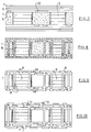
- FIG. 3 two Faltflex coils 4, 5 are shown. It is indicated that these are composed of several layers of folded film with coil turns. These Faltflex coils are known, they can have different sizes, shapes and different values.
- FIG. 5 shows the end result of the just described method, namely an induction component, which is formed as a self-contained piece of a printed circuit board and can now be electrically and mechanically connected in this state, for example, with another circuit board. It is also conceivable and possible for such an induction component to be part of a larger printed circuit board in which further functions are contained.
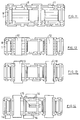
- FIG. 6 shows a method step in another manufacturing method, in which after the in FIG. 2 illustrated method step, this time with two cavities 3, first a circuit board layout 10 is applied to the two side surfaces of the core layer. Subsequently, in each case a Faltflex coil 5 are inserted into the two cavities 3. Thereafter, the two side surfaces of the core layer 1 are again laminated with a prepreg layer 6 and a metallic cover layer 7. This creates an intermediate that is in FIG. 8 shown is. So there are two levels of tracks on each side of the core layer. Now, a circuit board layout can again be formed on the outer metallic cover layer 7, so that the arrangement shown in section in FIG. 9 is produced. Again, it is an induction component with two Faltflex coils which are electrically connected by transversely through the circuit board passing conductor tracks 8 and the circuit board element on both sides.
- Faltflex coils 4, 5 may also be packages of coils in which a plurality of coils are pressed together so that they appear as a single component and can be used in this way in cavities.
- the induction component the in FIG. 10 is shown, the manufacturing operations are not shown in detail, since they run in principle the same as in the aforementioned embodiments.
- the connection from the outer level to the middle level is done by micro vias 11.
- FIGS. 9 and 10 While with in the FIGS. 9 and 10
- FIG. 11 an embodiment in which the AnARM mich the coil is not done by passing through them cross-connections, but with the help of printed conductor leads from the flat sides of the coil packages ago, for example by the microvias 11 in the FIG. 11 ,
- FIG. 12 shows a further embodiment, in which in an already largely manufactured induction component through recesses 12 are introduced, in which then ferrite cores 13 are used, see FIG. 13 ,
- FIG. 14 shows that on the outer layers of the circuit board additional electronic components 14 can be placed, which are also operatively connected to the induction component.
- further electronic components 15 are contained in intermediate layers within the core layer.
- the ferrite cores 13 are inserted later.
- the ends of the ferrite cores 13 are accessible from the outside of the induction component ago.
- FIG. 15 shown schematically.
- such a device 16 can be inserted into the cavity 3 of the core layer 1.
- a pressing is again carried out with a prepreg layer 6 and a metallic cover layer 7 on both sides. The further treatment then corresponds to what has been described so far.
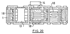
- FIG. 17 shows a component of pressed together Faltflex coils 4, on whose two peripheral sides 17 each have an electronic component 18 is attached, whose extension thus extends transversely to the surface of the core layer or circuit board.
- FIG. 18 It is also possible to arrange additional electronic components between the layers of a Faltflex coil. This is schematically in FIG. 18 shown.
- Starting point for a Faltflex coil is a film 19 with printed or otherwise arranged coil turns, which are arranged in a specific repeat, so that after folding then the coil turns are superimposed.
- electronic components 18 may be attached, for example, as discrete components, or printed. After folding, see FIG. 19 , These components 18 are then within the Faltflex coil, possibly also at different locations within this coil.
- FIG. 20 now shows an induction component, in which the different options described so far are combined.
- additional electronic components 18 are arranged within the circuit board, which are either connected to a Faltflex coil, or even independently of the Faltflex coil and are mounted independently of a cavity in the intermediate layer, as shown for example in the middle.
Landscapes
- Engineering & Computer Science (AREA)
- Power Engineering (AREA)
- Microelectronics & Electronic Packaging (AREA)
- Manufacturing & Machinery (AREA)
- Coils Or Transformers For Communication (AREA)
Description
Die Erfindung betrifft ein Induktionsbauteil mit mindestens einer, vorzugsweise mehreren Spulen. Derartige Induktionsbauteile werden in der Elektronik benötigt. Sie werden dabei in Zusammenhang mit Leiterplatten verwendet, mit deren Leiterbahnen sie elektrisch verbunden werden müssen.The invention relates to an induction component with at least one, preferably a plurality of coils. Such induction components are needed in electronics. They are used in connection with circuit boards, with their tracks they must be electrically connected.
Es ist bereits ein Induktionsbauteil bekannt (
Es ist bereits ein Verfahren zum Herstellen von ebenen Induktionsbauteilen bekannt, bei dem in eine Leiterplatte parallele langgestreckte Kanäle zur Aufnahme von Magnetkernmaterial und zwischen diesen angeordnete parallele Kanäle zur Aufnahme von leitendem Material zur Bildung von Windungen eingebracht werden (
Ebenfalls bekannt ist eine induktives Bauelement mit einem Magnetkern und Leiterstreifen, die durch ein Leiterplattensubstrat verlaufen und Teile der Spulenwicklungen bilden (
Der Erfindung liegt die Aufgabe zu Grunde, ein Induktionsbauteil mit mindestens einer Spule zu schaffen, das sich mit geringem Aufwand und wenigen Fehlermöglichkeiten herstellen lässt und sich zur Verbindung mit Leiterbahnen von Leiterplatten besonders gut geeignet.The invention is based on the object to provide an induction component with at least one coil, which can be produced with little effort and few possibilities for error and is particularly well suited for connection to printed conductors of printed circuit boards.
Zur Lösung dieser Aufgabe schlägt die Erfindung ein Induktionsbauteil mit den im Anspruch 1 genannten Merkmalen vor. Die Erfindung schlägt ebenfalls ein Verfahren zur Herstellung eines solchen Bauteils vor. Weiterbildungen der Erfindung sind Gegenstand der jeweiligen abhängigen Patentansprüche.To solve this problem, the invention proposes an induction component with the features mentioned in
Dieses von der Erfindung vorgeschlagene Induktionsbauteil enthält also die mindestens eine Spule in einem Hohlraum der Leiterplatte beziehungsweise eines Stücks Leiterplatte. Damit kann sowohl bei der Herstellung des Induktionsbauteils als auch bei der weiteren Verwendung des Induktionsbauteils auf alle bei der Herstellung und Handhabung von Leiterplatten üblichen, bekannten und bewährten Methoden und Vorgängen zurückgegriffen werden. Bei dem Bauteil handelt es sich also um ein Stück Leiterplatte.This proposed by the invention induction component thus contains the at least one coil in a cavity of the circuit board or a piece of printed circuit board. This can be both in the production the induction component as well as in the further use of the induction component on all in the manufacture and handling of printed circuit boards usual, known and proven methods and operations are recourse. The component is thus a piece of printed circuit board.
Zur Verbindung der Spulenwindungen mit den Leiterbahnen der Leiterplatte kann vorgesehen sein, dass die Windungsenden oder Anzapfungen der Windungen mit durch die Leiterplatte hindurch geführten Kontaktmitteln oder Vias verlötet sind.To connect the coil turns with the conductor tracks of the circuit board can be provided that the Windungsenden or taps of the turns are soldered to passing through the circuit board through contact means or vias.
Bei der mindestens einen Spule kann es sich um eine gewickelte Drahtspule oder auch um eine Faltflex- Spule handeln.The at least one coil may be a wound wire coil or a convoluted coil.
Ebenfalls möglich ist es, eine Spule als Planarspule herzustellen.It is also possible to produce a coil as a planar coil.
Auf die Faltflex Spule kann auch ein Magnet aufgedruckt werden.On the Faltflex coil also a magnet can be printed.
Als besonders sinnvoll hat es sich herausgestellt, wenn dieses Induktionsbauteil nicht nur eine oder mehrere Spulen enthält, sondern weitere für bestimmte Funktionen sinnvolle, nötige oder erforderliche elektrische, elektronische oder sonstige Bauteile.It has been found to be particularly useful if this induction component not only contains one or more coils, but further for certain functions useful, necessary or required electrical, electronic or other components.
Ein derartiges elektronisches Bauteil kann beispielsweise auch in dem Hohlraum untergebracht werden, in dem die Spule angeordnet wird. Dieses Bauteil kann horizontal, also parallel zur Außenseite der Leiterplatte, oder auch vertikal eingebracht werden. Dies kann unabhängig von der einzusetzenden Spule, also vorkonfektioniert, erfolgen. Es ist ebenfalls möglich, dass dieses zusätzliche Bauelement auf der einzusetzenden Spule angeordnet, also mit dieser verbunden ist.Such an electronic component can for example also be accommodated in the cavity in which the coil is arranged. This component can be placed horizontally, ie parallel to the outside of the circuit board, or vertically. This can be done independently of the coil to be used, ie prefabricated. It is also possible that this additional component is arranged on the coil to be used, that is connected to this.
Es ist ebenfalls möglich und wird von der Erfindung vorgeschlagen, dass ein zusätzliches elektronisches Bauelement unabhängig von einer einzusetzenden Spule direkt in einer Schicht einer Multilayerleiterplatte eingebracht wird.It is also possible and is proposed by the invention that an additional electronic component is introduced directly into a layer of a multilayer printed circuit board independently of a coil to be inserted.
Insbesondere kann in Weiterbildung der Erfindung vorgesehen sein, dass in einem Hohlraum mehrere Spulen angeordnet sind, die vorzugsweise übereinander geschichtet sind. Diese Spulen können getrennt elektrisch mit Leiterbahnen der Leiterplatte verbunden sein, oder auch zusammenwirken.In particular, it can be provided in a further development of the invention that several coils are arranged in a cavity, which are preferably stacked on top of each other. These coils may be separately electrically connected to tracks of the circuit board, or also cooperate.
Insbesondere kann in Weiterbildung vorgesehen sein, dass mehrere für einen Hohlraum bestimmte Spulen miteinander verpresst sind, so dass sie ein einziges Bauteil bilden, das sich dann als ein Element verarbeiten und in den Hohlraum der Leiterplatte einsetzen lässt.In particular, it can be provided in a development that several coils intended for a cavity are pressed together, so that they form a single component, which can then be processed as an element and inserted into the cavity of the circuit board.
Eine weitere Möglichkeit besteht darin, dass eine einzelne Faltflex Spule mehrere getrennte Spulen aufweist, die durch ein entsprechendes Layout auf der Folie verwirklicht sind, bevor diese gefaltet wird. Natürlich sind auch Kombinationen möglich, wonach Faltflex Einrichtungen mit mehreren Spulen miteinander verpresst sind.Another possibility is that a single Faltflex coil having a plurality of separate coils, which are realized by a corresponding layout on the film before it is folded. Of course, combinations are also possible, according to which Faltflex devices with several coils are pressed together.
Erfindungsgemäß kann vorgesehen sein, dass es sich bei der Leiterplatte auch um eine Multilayerleiterplatte handelt, insbesondere dann, wenn weitere Funktionen in dem Induktionsbauteil untergebracht werden sollen.According to the invention, it may be provided that the printed circuit board is also a multilayer printed circuit board, in particular if further functions are to be accommodated in the induction component.
Erfindungsgemäß kann in Weiterbildung vorgesehen sein, dass das Induktionsbauteil einen diskreten oder auch einen gedruckten Ferritkern für die Spule aufweist.According to the invention may be provided in a development that the induction component has a discrete or a printed ferrite core for the coil.
Es wurde bereits erwähnt, dass das Induktionsbauteil gegebenenfalls auch ein weiteres elektronisches Bauteil enthalten kann. Erfindungsgemäß kann in Weiterbildung vorgesehen sein, ein solches Bauteil nicht nur in einem Hohlraum der Leiterplatte unterzubringen, sondern auch an einer Außenlage der Leiterplatte.It has already been mentioned that the induction component may possibly also contain a further electronic component. According to the invention may be provided in a further development to accommodate such a component not only in a cavity of the circuit board, but also on an outer layer of the circuit board.
Es ist andererseits auch möglich, ein weiteres Bauteil an einer Innenlage unabhängig von dem Hohlraum für die Spule anzuordnen.On the other hand, it is also possible to arrange a further component on an inner layer independently of the cavity for the coil.
Die Anordnung eines Bauteils an einer Innenlage kann entweder eine diskrete Bestückung mit dem Bauteil sein, oder auch einen Aufdrucken eines solchen Bauteils.The arrangement of a component on an inner layer can either be a discrete component with the component, or even a printing of such a component.
Die Zusammenfassung mehrerer Spulen durch Verpressen zur Bildung eines einzelnen handhabbaren Bestandteils eines Induktionsbauteils nach der Erfindung kann auch derart geschehen, dass diesem Bauteil ein Ferritkern hinzugefügt wird, so dass wiederum ein einzeln handhabbares Bestandteil zum Einsetzen in einen Hohlraum der Leiterplatte entsteht.The combination of several coils by compression to form a single manageable component of an induction component according to the invention can also be done in such a way that a ferrite core is added to this component, so that again an individually manageable component for insertion into a cavity of the printed circuit board is formed.
Der Ferritkern, bei dem es sich beispielsweise um einen Ringkern, oder auch um einen U-Kern oder einen E-Kern handeln kann, kann so angeordnet werden, dass er auf beiden Seiten aus den Spulen herausragt und auch aus der zusammengefügten Leiterplatte.The ferrite core, which may be, for example, a toroidal core, or a U-core or an E-core, may be arranged to protrude from both sides of the coils and also from the assembled circuit board.
Andererseits ist es aber auch möglich, einen Ferritkern so anzuordnen, dass er beim Verschließen des Hohlraums durch Laminieren ebenfalls vollständig innerhalb der Leiterplatte angeordnet ist.On the other hand, it is also possible to arrange a ferrite core so that it is also completely disposed within the circuit board when the cavity is closed by lamination.
In Weiterbildung der Erfindung kann vorgesehen sein, dass eine Faltflex als elektronisches Bauteil mit Induktivitätsanteil und/oder Kapazitätsanteil und/oder Widerstandsanteil ausgebildet ist. Somit kann das Induktionsbauteil ein Element aufweisen, das als Induktivität, Kapazität und/oder Widerstand alleine oder auch in Kombination mit der Bedruckung beziehungsweise Bestückung verwendet werden kann.In a further development of the invention it can be provided that a Faltflex is formed as an electronic component with inductance component and / or capacitance component and / or resistance component. Thus, the induction component have an element that can be used as an inductance, capacitance and / or resistance alone or in combination with the printing or assembly.
Das Verfahren zum Herstellen eines solchen Induktionsbauteils läuft so ab, dass in die Kernschicht eines Stücks Leiterplatte ein Hohlraum eingebracht wird. In diese Ausnehmung wird die Spule oder ein Paket von Spulen eingebracht. Anschließend wird die Ausnehmung dadurch verschlossen, dass beidseits ein Prepreg und anschließend eine metallische Deckschicht auflaminiert wird. Die elektrisch leitende Verbindung kann dann in bekannter Weise erfolgen.The method for producing such an induction component is such that a cavity is introduced into the core layer of a piece of printed circuit board. In this recess, the coil or a package of coils is introduced. Subsequently, the recess is closed by laminating a prepreg on both sides and then a metallic cover layer. The electrically conductive connection can then take place in a known manner.
Falls die Leiterplatte beidseits mit einer metallischen Deckschicht versehen ist, kann diese metallische Deckschicht auf einer Seite oder auf beiden Seiten vorher entfernt werden. Das Entfernen der Deckschicht kann beispielsweise in einem Arbeitsgang mit der Herstellung der Ausnehmung erfolgen, die nach Herstellung einen Hohlraum in der Leiterplatte bildet.If the circuit board is provided on both sides with a metallic cover layer, this metallic cover layer on one side or on both sides can be removed beforehand. The removal of the cover layer can be done for example in one operation with the production of the recess, which forms a cavity in the circuit board after manufacture.
Zur Anbringung eines Bauelements auf einer Innenlage, beispielsweise sogar einer Innenlage einer Spule, kann vorgesehen sein, dass auf einer mit Spulenwindungen bedruckten Folie vor deren Falten die weiteren Bauteile angebracht werden, entweder durch eine Vorbestückung oder durch ein Aufdrucken.For attaching a component on an inner layer, for example, even an inner layer of a coil, it can be provided that the other components are mounted on a printed with coil turns foil before their folds, either by Vorbestückung or by imprinting.
Einen Ferritkern, der mehreren Spulen gemeinsam sein soll, kann beispielsweise vor dem Einbringen der Spulen in den Hohlraum der Leiterplatte mit diesen verbunden werden.A ferrite core, which is to be common to several coils, can be connected, for example, before introducing the coils into the cavity of the printed circuit board with these.
Weitere Merkmale, Einzelheiten und Vorzüge der Erfindung ergeben sich aus den Ansprüchen und der Zusammenfassung, deren beider Wortlaut durch Bezugnahme zum Inhalt der Beschreibung gemacht wird, der folgenden Beschreibung bevorzugter Ausführungsformen der Erfindung sowie anhand der Zeichnung. Hierbei zeigen:
Figur 1- einen Schnitt durch eine Leiterplatte vor ihrer Bearbeitung;
Figur 2- den Schnitt durch die Leiterplatte nach Herstellung eines Hohlraums;
Figur 3- schematisch zwei verschieden große Faltflex Spulen;
Figur 4- die Anordnung einer Faltflex Spule in dem Hohlraum;
Figur 5 den- Schnitt durch die Leiterplatte nach ihrer Kontaktierung;
Figur 6- einen Schnitt durch eine Leiterplatte mit Kontakten und zwei Hohlräumen;
Figur 7- einen der
Figur 4 entsprechenden Schnitt bei der Ausführungsform derFigur 6 ; Figur 8- den
Schnitt der Figur 7 nach Laminierung der inFigur 7 Figur 9- das endgültige Ergebnis der Bearbeitung der Ausführungsform nach
den Figuren 6 ;bis 8 Figur 10- das Ergebnis einer Bearbeitung einer Leiterplatte mit zwei Prepregschichten;
Figur 11- einen Schnitt durch eine gegenüber der Leiterplatte der
Figur 10 geänderte Ausführungsform; Figur 12- eine Ausführungsform mit durch die Leiterplatte durchgehenden Öffnungen;
Figur 13- der Ausführungsform der
Figur 12 mit eingesetztem Ferritkern; Figur 14- die
Ausführungsform der Figur 12 und 13 nach Fertigstellung mit zusätzlichen Bauteilen; Figur 15- zwei Faltflex Spulen mit vorher eingesetztem Ferritkern;
Figur 16eine den Figuren 4 und7 entsprechende Darstellung mit denSpulen der Figur 15 ;Figur 17- eine Faltflex Spule mit seitlich angebrachten weiteren Bauelementen;
Figur 18- eine mit Spulenwindungen versehene Folie mit aufgesetzten Bauelementen;
Figur 19- die durch das Falten der Folie der
Figur 18 hergestellte Faltflex Spule; - Figur 20
- schematisch einen Schnitt durch eine Leiterplatte mit den
Spulen der Figur 17 und .Figur 19
- FIG. 1
- a section through a circuit board before its processing;
- FIG. 2
- the section through the circuit board after making a cavity;
- FIG. 3
- schematically two different sized Faltflex coils;
- FIG. 4
- the arrangement of a Faltflex coil in the cavity;
- Figure 5 the
- Section through the printed circuit board after contacting;
- FIG. 6
- a section through a printed circuit board with contacts and two cavities;
- FIG. 7
- one of the
FIG. 4 corresponding section in the embodiment of theFIG. 6 ; - FIG. 8
- the cut of the
FIG. 7 after lamination of inFIG. 7 still separate layers; - FIG. 9
- the final result of processing the embodiment according to the
FIGS. 6 to 8 ; - FIG. 10
- the result of processing a printed circuit board with two prepreg layers;
- FIG. 11
- a section through a relative to the circuit board of the
FIG. 10 modified embodiment; - FIG. 12
- an embodiment with through the circuit board through openings;
- FIG. 13
- the embodiment of the
FIG. 12 with inserted ferrite core; - FIG. 14
- the embodiment of the
FIGS. 12 and 13 after completion with additional components; - FIG. 15
- two Faltflex coils with previously inserted ferrite core;
- FIG. 16
- a the
FIGS. 4 and7 corresponding representation with the coils ofFIG. 15 ; - FIG. 17
- a Faltflex coil with laterally mounted further components;
- FIG. 18
- a coil-wound foil with attached components;
- FIG. 19
- which by folding the film of the
FIG. 18 manufactured Faltflex coil; - FIG. 20
- schematically a section through a printed circuit board with the coils of
FIG. 17 and FIG. 19 ,
Ausgangspunkt für die Herstellung des Induktionsbauteils nach der Erfindung ist eine übliche Leiterplatte mit einer Kernschicht 1 und zwei metallischen Deckschichten 2. Zunächst werden die Deckschichten 2 entfernt, so dass nur die Kernschicht 1 übrig bleibt. In diese Kernschicht 1 wird ein Hohlraum 3 eingebracht, die im dargestellten Beispiel von der einen Seite zu der anderen Seite der Kernschicht 1 durchgeht.The starting point for the production of the induction component according to the invention is a conventional printed circuit board with a
In
Die in
Dann werden die metallischen Deckschichten 7 auf beiden Seiten durch die dazwischenliegenden Schichten hindurch mit durchkontaktierten Bohrungen miteinander verbundenen, wobei diese durchgehenden Leitungen 8 auch durch die Faltflex Spule 4 hindurch gehen und diese kontaktieren. Dies ist in
Die
Bei den nur schematisch angedeuteten Faltflex Spulen 4, 5 kann es sich auch um Pakete von Spulen handeln, bei denen mehrere Spulen miteinander verpresst sind, so dass sie als ein einziges Bauteil erscheinen und in dieser Weise in Hohlräume eingesetzt werden können.The only schematically indicated Faltflex coils 4, 5 may also be packages of coils in which a plurality of coils are pressed together so that they appear as a single component and can be used in this way in cavities.
Bei dem Induktionsbauteil, das in
Während bei den in den
Die
Bei der Ausführungsform, die in den
Die
Es ist ebenfalls möglich, zusätzliche elektronische Bauelemente zwischen den Lagen einer Faltflex Spule anzuordnen. Dies ist schematisch in
Claims (29)
- Induction component, including1.1 a circuit board,1.2 at least one cavity (3) in the circuit board,1.3 at least one coil (4, 5) disposed within said cavity (3),1.4 said coil being electrically connected to conductor paths of the circuit board, wherein1.5 the cavity (3) is closed on both sides of the circuit board.
- Induction component according to claim 1, wherein at least one coil is a Foldflex (Faltflex) coil (4, 5).
- Induction component according to claim 1 or 2, wherein at least one coil is a planar coil.
- Induction component according to any one of the preceding claims, wherein the circuit board includes further components (9, 15, 18).
- Induction component according to any one of the preceding claims, wherein a further electronic component (18) is disposed within the cavity (3) in which the coil is accommodated.
- Induction component according to any one of the preceding claims, wherein a plurality of coils is disposed within the cavity (3), preferably are stacked one upon the other.
- Induction component according to any one of the preceding claims, wherein a plurality of coils are pressed together and combined to one device (16).
- Induction component according to any one of the preceding claims, having at least one discrete ferrite core (13).
- Induction component according to any one of the preceding claims, having at least one printed ferrite core (13).
- Induction component according to any one of the preceding claims, having at least one further device (14) attached on the outer layer.
- Induction component according to any one of the preceding claims, wherein an inner layer of the circuit board is assembled with at least one device (15).
- Induction component according to any one of the preceding claims, wherein a device is printed on at least one inner layer.
- Induction component according to any one of the preceding claims, having at least one ferrite core (13) traversing a plurality of coils and pressed therewith.
- Induction component according to claim 13, wherein at least one ferrite core (13) projects outwards on at least one outer side of the circuit board.
- Induction component according to claim 13 or 14, wherein at least one ferrite core (13) is covered by the circuit board completely on both sides.
- Induction component according to any one of the preceding claims, wherein the circuit board is a multilayer circuit board.
- Induction component according to any one of the preceding claims, wherein a Foldflex is an electronic component including an inductance portion and/or a capacitance portion and/or a resistance portion.
- Method for the production of an induction component, comprising the following method steps:18.1 producing a cavity (3) in a core layer (1) of a circuit board,18.2 placing a pre-fabricated coil (4, 5) into the cavity (3),18.3 laminating the circuit board with a pre-preg layer (6) and a metallic cover layer (7) on the one or more side(s) of the opening of the cavity (3),18.4 producing vias or through contact connection means (8) and contacting them on the outer side of the circuit board in order to contact the coil windings.
- Method according to claim 18, wherein said contacting of the coil (4, 5) is from the inner side of the cavity (3) and/or from the outer side of the circuit board.
- Method according to claim 18 or 19, wherein using a circuit board coated on both sides, the metallic cover layer (2) is removed from at least one side.
- Method according to any of claims 18 to 20, wherein a device (18) is placed in vertically.
- Method according to any of claims 18 to 21, wherein a device (15) is attached on at least one inner layer.
- Method according to any of claims 18 to 22, wherein a device (14) is attached on at least one outer layer.
- Method according to any of claims 18 to 23, wherein a plurality of coils are pressed together to produce one device (16).
- Method according to any of claims 18 to 24, wherein a ferrite core (13) is placed in the circuit board.
- Method according to any of claims 18 to 25, wherein a ferrite core (13) is placed in interconnected coils and subsequently is inserted into the cavity (3) of the circuit board.
- Method according to any of claims 18 to 26, wherein interconnected coils are pre-assembled with further components (18) and subsequently are inserted into the cavity (3).
- Method according to any of claims 18 to 27, wherein a film (19) with printed-on coil windings is pre-assembled and/or printed with further components (18) prior to folding.
- Method according to any of claims 18 to 28, wherein a multilayer circuit board is used.
Priority Applications (1)
| Application Number | Priority Date | Filing Date | Title |
|---|---|---|---|
| EP09004651.7A EP2107577B1 (en) | 2008-03-31 | 2009-03-31 | Inductive component and method for its production |
Applications Claiming Priority (3)
| Application Number | Priority Date | Filing Date | Title |
|---|---|---|---|
| DE200810017303 DE102008017303A1 (en) | 2008-03-31 | 2008-03-31 | inductance component |
| EP08162811.7A EP2107576B1 (en) | 2008-03-31 | 2008-08-22 | Induction component |
| EP09004651.7A EP2107577B1 (en) | 2008-03-31 | 2009-03-31 | Inductive component and method for its production |
Publications (2)
| Publication Number | Publication Date |
|---|---|
| EP2107577A1 EP2107577A1 (en) | 2009-10-07 |
| EP2107577B1 true EP2107577B1 (en) | 2016-10-19 |
Family
ID=40674084
Family Applications (1)
| Application Number | Title | Priority Date | Filing Date |
|---|---|---|---|
| EP09004651.7A Not-in-force EP2107577B1 (en) | 2008-03-31 | 2009-03-31 | Inductive component and method for its production |
Country Status (1)
| Country | Link |
|---|---|
| EP (1) | EP2107577B1 (en) |
Families Citing this family (3)
| Publication number | Priority date | Publication date | Assignee | Title |
|---|---|---|---|---|
| EP3340260B1 (en) * | 2016-12-22 | 2022-03-23 | AT & S Austria Technologie & Systemtechnik Aktiengesellschaft | Inductor made of component carrier material comprising electrically conductive plate structures |
| DE102018114785A1 (en) | 2018-04-13 | 2019-10-17 | Trafag Ag | Method for producing a planar coil arrangement and a sensor head provided therewith |
| US11398334B2 (en) * | 2018-07-30 | 2022-07-26 | At&S Austria Technologie & Systemtechnik Aktiengesellschaft | Component carrier comprising embedded inductor with an inlay |
Family Cites Families (5)
| Publication number | Priority date | Publication date | Assignee | Title |
|---|---|---|---|---|
| US5781091A (en) * | 1995-07-24 | 1998-07-14 | Autosplice Systems Inc. | Electronic inductive device and method for manufacturing |
| DE19723068C1 (en) | 1997-06-02 | 1999-05-12 | Vacuumschmelze Gmbh | Inductive component |
| US6662431B1 (en) | 1997-08-06 | 2003-12-16 | Halo Electronics, Inc. | Electronic surface mount package |
| US6990725B2 (en) | 2001-10-05 | 2006-01-31 | Fontanella Mark D | Fabrication approaches for the formation of planar inductors and transformers |
| DE10154833A1 (en) * | 2001-11-08 | 2003-05-22 | Infineon Technologies Ag | Inductor and process for its manufacture |
-
2009
- 2009-03-31 EP EP09004651.7A patent/EP2107577B1/en not_active Not-in-force
Also Published As
| Publication number | Publication date |
|---|---|
| EP2107577A1 (en) | 2009-10-07 |
Similar Documents
| Publication | Publication Date | Title |
|---|---|---|
| DE69510630T2 (en) | LADDER FRAME WITH AN INDUCTOR OR SIMILAR MAGNETIC COMPONENT | |
| EP0473875B1 (en) | Method for producing a HF-magnetic coil device in chip-construction | |
| DE19508011C2 (en) | Electromagnetic valve unit | |
| DE4422827C2 (en) | Layered encapsulated electrical winding, transformer unit and process for its manufacture | |
| DE102009046183A1 (en) | Device with a magnetic component and method for its production | |
| WO2014139674A1 (en) | Electronic sub-assembly and method for the production of an electronic sub-assembly | |
| WO2016193017A1 (en) | Planar transformer for energy transfer | |
| EP3547338A1 (en) | Electronic component and method for its manufacture | |
| DE102007028239A1 (en) | Monolithic inductive component, method for manufacturing the component and use of the component | |
| DE4337053A1 (en) | Kitchen sink | |
| EP2107577B1 (en) | Inductive component and method for its production | |
| WO2008104324A1 (en) | Method for incorporating chips in circuit board cavities | |
| EP2107576B1 (en) | Induction component | |
| DE3722124A1 (en) | Printed circuit board assembly having a coil or a transformer | |
| EP1971193A1 (en) | PCB component for manufacturing planar inductances with closed inner forms | |
| WO2013057266A1 (en) | High voltage transformer and wound coil former for ignition modules with terminal pins integral to the primary winding | |
| DE2917388C2 (en) | ||
| WO2015176919A1 (en) | Multilayer inductive passive component and film body for the production thereof | |
| DE102018005043A1 (en) | Planar | |
| EP3475960A1 (en) | Transformer device and method for manufacturing same | |
| DE112021001622T5 (en) | MULTI-STAGE PROCESS BUILT DOUBLE WINDING EMBEDDED SOLENOID INDUCTOR | |
| DE202019102273U1 (en) | Inductive component | |
| DE102007028240B3 (en) | Production of a ceramic multiple layered body used in the production of e.g. strip conductors comprises preparing a first ceramic green foil having openings and further ceramic green foils, bringing the green foils together and laminating | |
| DE10257321A1 (en) | Manufacture of electronic components such as inductors or transformers, by applying structured layers of conductive and insulating materials in form of viscose paste, so that connection points are in contact | |
| WO2003041094A1 (en) | Inductor and a method for producing the same |
Legal Events
| Date | Code | Title | Description |
|---|---|---|---|
| PUAI | Public reference made under article 153(3) epc to a published international application that has entered the european phase |
Free format text: ORIGINAL CODE: 0009012 |
|
| AK | Designated contracting states |
Kind code of ref document: A1 Designated state(s): AT BE BG CH CY CZ DE DK EE ES FI FR GB GR HR HU IE IS IT LI LT LU LV MC MK MT NL NO PL PT RO SE SI SK TR |
|
| AX | Request for extension of the european patent |
Extension state: AL BA RS |
|
| 17P | Request for examination filed |
Effective date: 20100222 |
|
| 17Q | First examination report despatched |
Effective date: 20100324 |
|
| AKX | Designation fees paid |
Designated state(s): AT BE BG CH CY CZ DE DK EE ES FI FR GB GR HR HU IE IS IT LI LT LU LV MC MK MT NL NO PL PT RO SE SI SK TR |
|
| REG | Reference to a national code |
Ref country code: DE Ref legal event code: R079 Ref document number: 502009013237 Country of ref document: DE Free format text: PREVIOUS MAIN CLASS: H01F0027060000 Ipc: H01F0017000000 |
|
| RIC1 | Information provided on ipc code assigned before grant |
Ipc: H05K 1/18 20060101ALI20160414BHEP Ipc: H01F 17/00 20060101AFI20160414BHEP Ipc: H01F 27/28 20060101ALI20160414BHEP Ipc: H01F 17/04 20060101ALI20160414BHEP Ipc: H01F 41/04 20060101ALI20160414BHEP Ipc: H05K 3/46 20060101ALI20160414BHEP |
|
| GRAP | Despatch of communication of intention to grant a patent |
Free format text: ORIGINAL CODE: EPIDOSNIGR1 |
|
| INTG | Intention to grant announced |
Effective date: 20160524 |
|
| GRAS | Grant fee paid |
Free format text: ORIGINAL CODE: EPIDOSNIGR3 |
|
| GRAA | (expected) grant |
Free format text: ORIGINAL CODE: 0009210 |
|
| AK | Designated contracting states |
Kind code of ref document: B1 Designated state(s): AT BE BG CH CY CZ DE DK EE ES FI FR GB GR HR HU IE IS IT LI LT LU LV MC MK MT NL NO PL PT RO SE SI SK TR |
|
| REG | Reference to a national code |
Ref country code: GB Ref legal event code: FG4D Free format text: NOT ENGLISH |
|
| REG | Reference to a national code |
Ref country code: CH Ref legal event code: NV Representative=s name: DR. LUSUARDI AG, CH Ref country code: CH Ref legal event code: EP |
|
| REG | Reference to a national code |
Ref country code: AT Ref legal event code: REF Ref document number: 838945 Country of ref document: AT Kind code of ref document: T Effective date: 20161115 |
|
| REG | Reference to a national code |
Ref country code: IE Ref legal event code: FG4D Free format text: LANGUAGE OF EP DOCUMENT: GERMAN |
|
| REG | Reference to a national code |
Ref country code: DE Ref legal event code: R096 Ref document number: 502009013237 Country of ref document: DE |
|
| REG | Reference to a national code |
Ref country code: NL Ref legal event code: MP Effective date: 20161019 |
|
| REG | Reference to a national code |
Ref country code: LT Ref legal event code: MG4D |
|
| PG25 | Lapsed in a contracting state [announced via postgrant information from national office to epo] |
Ref country code: LV Free format text: LAPSE BECAUSE OF FAILURE TO SUBMIT A TRANSLATION OF THE DESCRIPTION OR TO PAY THE FEE WITHIN THE PRESCRIBED TIME-LIMIT Effective date: 20161019 |
|
| REG | Reference to a national code |
Ref country code: FR Ref legal event code: PLFP Year of fee payment: 9 |
|
| PG25 | Lapsed in a contracting state [announced via postgrant information from national office to epo] |
Ref country code: SE Free format text: LAPSE BECAUSE OF FAILURE TO SUBMIT A TRANSLATION OF THE DESCRIPTION OR TO PAY THE FEE WITHIN THE PRESCRIBED TIME-LIMIT Effective date: 20161019 Ref country code: LT Free format text: LAPSE BECAUSE OF FAILURE TO SUBMIT A TRANSLATION OF THE DESCRIPTION OR TO PAY THE FEE WITHIN THE PRESCRIBED TIME-LIMIT Effective date: 20161019 Ref country code: NO Free format text: LAPSE BECAUSE OF FAILURE TO SUBMIT A TRANSLATION OF THE DESCRIPTION OR TO PAY THE FEE WITHIN THE PRESCRIBED TIME-LIMIT Effective date: 20170119 Ref country code: GR Free format text: LAPSE BECAUSE OF FAILURE TO SUBMIT A TRANSLATION OF THE DESCRIPTION OR TO PAY THE FEE WITHIN THE PRESCRIBED TIME-LIMIT Effective date: 20170120 |
|
| PG25 | Lapsed in a contracting state [announced via postgrant information from national office to epo] |
Ref country code: HR Free format text: LAPSE BECAUSE OF FAILURE TO SUBMIT A TRANSLATION OF THE DESCRIPTION OR TO PAY THE FEE WITHIN THE PRESCRIBED TIME-LIMIT Effective date: 20161019 Ref country code: IS Free format text: LAPSE BECAUSE OF FAILURE TO SUBMIT A TRANSLATION OF THE DESCRIPTION OR TO PAY THE FEE WITHIN THE PRESCRIBED TIME-LIMIT Effective date: 20170219 Ref country code: FI Free format text: LAPSE BECAUSE OF FAILURE TO SUBMIT A TRANSLATION OF THE DESCRIPTION OR TO PAY THE FEE WITHIN THE PRESCRIBED TIME-LIMIT Effective date: 20161019 Ref country code: ES Free format text: LAPSE BECAUSE OF FAILURE TO SUBMIT A TRANSLATION OF THE DESCRIPTION OR TO PAY THE FEE WITHIN THE PRESCRIBED TIME-LIMIT Effective date: 20161019 Ref country code: PL Free format text: LAPSE BECAUSE OF FAILURE TO SUBMIT A TRANSLATION OF THE DESCRIPTION OR TO PAY THE FEE WITHIN THE PRESCRIBED TIME-LIMIT Effective date: 20161019 Ref country code: PT Free format text: LAPSE BECAUSE OF FAILURE TO SUBMIT A TRANSLATION OF THE DESCRIPTION OR TO PAY THE FEE WITHIN THE PRESCRIBED TIME-LIMIT Effective date: 20170220 Ref country code: NL Free format text: LAPSE BECAUSE OF FAILURE TO SUBMIT A TRANSLATION OF THE DESCRIPTION OR TO PAY THE FEE WITHIN THE PRESCRIBED TIME-LIMIT Effective date: 20161019 |
|
| REG | Reference to a national code |
Ref country code: DE Ref legal event code: R097 Ref document number: 502009013237 Country of ref document: DE |
|
| PG25 | Lapsed in a contracting state [announced via postgrant information from national office to epo] |
Ref country code: RO Free format text: LAPSE BECAUSE OF FAILURE TO SUBMIT A TRANSLATION OF THE DESCRIPTION OR TO PAY THE FEE WITHIN THE PRESCRIBED TIME-LIMIT Effective date: 20161019 Ref country code: SK Free format text: LAPSE BECAUSE OF FAILURE TO SUBMIT A TRANSLATION OF THE DESCRIPTION OR TO PAY THE FEE WITHIN THE PRESCRIBED TIME-LIMIT Effective date: 20161019 Ref country code: CZ Free format text: LAPSE BECAUSE OF FAILURE TO SUBMIT A TRANSLATION OF THE DESCRIPTION OR TO PAY THE FEE WITHIN THE PRESCRIBED TIME-LIMIT Effective date: 20161019 Ref country code: EE Free format text: LAPSE BECAUSE OF FAILURE TO SUBMIT A TRANSLATION OF THE DESCRIPTION OR TO PAY THE FEE WITHIN THE PRESCRIBED TIME-LIMIT Effective date: 20161019 Ref country code: DK Free format text: LAPSE BECAUSE OF FAILURE TO SUBMIT A TRANSLATION OF THE DESCRIPTION OR TO PAY THE FEE WITHIN THE PRESCRIBED TIME-LIMIT Effective date: 20161019 |
|
| PLBE | No opposition filed within time limit |
Free format text: ORIGINAL CODE: 0009261 |
|
| STAA | Information on the status of an ep patent application or granted ep patent |
Free format text: STATUS: NO OPPOSITION FILED WITHIN TIME LIMIT |
|
| PG25 | Lapsed in a contracting state [announced via postgrant information from national office to epo] |
Ref country code: IT Free format text: LAPSE BECAUSE OF FAILURE TO SUBMIT A TRANSLATION OF THE DESCRIPTION OR TO PAY THE FEE WITHIN THE PRESCRIBED TIME-LIMIT Effective date: 20161019 Ref country code: BG Free format text: LAPSE BECAUSE OF FAILURE TO SUBMIT A TRANSLATION OF THE DESCRIPTION OR TO PAY THE FEE WITHIN THE PRESCRIBED TIME-LIMIT Effective date: 20170119 |
|
| 26N | No opposition filed |
Effective date: 20170720 |
|
| PG25 | Lapsed in a contracting state [announced via postgrant information from national office to epo] |
Ref country code: SI Free format text: LAPSE BECAUSE OF FAILURE TO SUBMIT A TRANSLATION OF THE DESCRIPTION OR TO PAY THE FEE WITHIN THE PRESCRIBED TIME-LIMIT Effective date: 20161019 Ref country code: MC Free format text: LAPSE BECAUSE OF FAILURE TO SUBMIT A TRANSLATION OF THE DESCRIPTION OR TO PAY THE FEE WITHIN THE PRESCRIBED TIME-LIMIT Effective date: 20161019 |
|
| REG | Reference to a national code |
Ref country code: IE Ref legal event code: MM4A |
|
| PG25 | Lapsed in a contracting state [announced via postgrant information from national office to epo] |
Ref country code: LU Free format text: LAPSE BECAUSE OF NON-PAYMENT OF DUE FEES Effective date: 20170331 |
|
| PG25 | Lapsed in a contracting state [announced via postgrant information from national office to epo] |
Ref country code: IE Free format text: LAPSE BECAUSE OF NON-PAYMENT OF DUE FEES Effective date: 20170331 |
|
| REG | Reference to a national code |
Ref country code: BE Ref legal event code: MM Effective date: 20170331 |
|
| PG25 | Lapsed in a contracting state [announced via postgrant information from national office to epo] |
Ref country code: BE Free format text: LAPSE BECAUSE OF NON-PAYMENT OF DUE FEES Effective date: 20170331 |
|
| REG | Reference to a national code |
Ref country code: FR Ref legal event code: PLFP Year of fee payment: 10 |
|
| PG25 | Lapsed in a contracting state [announced via postgrant information from national office to epo] |
Ref country code: MT Free format text: LAPSE BECAUSE OF FAILURE TO SUBMIT A TRANSLATION OF THE DESCRIPTION OR TO PAY THE FEE WITHIN THE PRESCRIBED TIME-LIMIT Effective date: 20161019 |
|
| PG25 | Lapsed in a contracting state [announced via postgrant information from national office to epo] |
Ref country code: HU Free format text: LAPSE BECAUSE OF FAILURE TO SUBMIT A TRANSLATION OF THE DESCRIPTION OR TO PAY THE FEE WITHIN THE PRESCRIBED TIME-LIMIT; INVALID AB INITIO Effective date: 20090331 |
|
| PG25 | Lapsed in a contracting state [announced via postgrant information from national office to epo] |
Ref country code: CY Free format text: LAPSE BECAUSE OF NON-PAYMENT OF DUE FEES Effective date: 20161019 |
|
| PG25 | Lapsed in a contracting state [announced via postgrant information from national office to epo] |
Ref country code: MK Free format text: LAPSE BECAUSE OF FAILURE TO SUBMIT A TRANSLATION OF THE DESCRIPTION OR TO PAY THE FEE WITHIN THE PRESCRIBED TIME-LIMIT Effective date: 20161019 |
|
| PG25 | Lapsed in a contracting state [announced via postgrant information from national office to epo] |
Ref country code: TR Free format text: LAPSE BECAUSE OF FAILURE TO SUBMIT A TRANSLATION OF THE DESCRIPTION OR TO PAY THE FEE WITHIN THE PRESCRIBED TIME-LIMIT Effective date: 20161019 |
|
| PGFP | Annual fee paid to national office [announced via postgrant information from national office to epo] |
Ref country code: GB Payment date: 20200323 Year of fee payment: 12 Ref country code: DE Payment date: 20200320 Year of fee payment: 12 Ref country code: AT Payment date: 20200320 Year of fee payment: 12 |
|
| PGFP | Annual fee paid to national office [announced via postgrant information from national office to epo] |
Ref country code: CH Payment date: 20200319 Year of fee payment: 12 |
|
| PGFP | Annual fee paid to national office [announced via postgrant information from national office to epo] |
Ref country code: FR Payment date: 20200320 Year of fee payment: 12 |
|
| REG | Reference to a national code |
Ref country code: DE Ref legal event code: R119 Ref document number: 502009013237 Country of ref document: DE |
|
| REG | Reference to a national code |
Ref country code: CH Ref legal event code: PL |
|
| REG | Reference to a national code |
Ref country code: AT Ref legal event code: MM01 Ref document number: 838945 Country of ref document: AT Kind code of ref document: T Effective date: 20210331 |
|
| GBPC | Gb: european patent ceased through non-payment of renewal fee |
Effective date: 20210331 |
|
| PG25 | Lapsed in a contracting state [announced via postgrant information from national office to epo] |
Ref country code: LI Free format text: LAPSE BECAUSE OF NON-PAYMENT OF DUE FEES Effective date: 20210331 Ref country code: AT Free format text: LAPSE BECAUSE OF NON-PAYMENT OF DUE FEES Effective date: 20210331 Ref country code: CH Free format text: LAPSE BECAUSE OF NON-PAYMENT OF DUE FEES Effective date: 20210331 Ref country code: GB Free format text: LAPSE BECAUSE OF NON-PAYMENT OF DUE FEES Effective date: 20210331 Ref country code: FR Free format text: LAPSE BECAUSE OF NON-PAYMENT OF DUE FEES Effective date: 20210331 Ref country code: DE Free format text: LAPSE BECAUSE OF NON-PAYMENT OF DUE FEES Effective date: 20211001 |