EP2107559A1 - Production method of magnetic transfer master carrier, magnetic transfer master carrier, magnetic transfer method, and magnetic recording medium - Google Patents
Production method of magnetic transfer master carrier, magnetic transfer master carrier, magnetic transfer method, and magnetic recording medium Download PDFInfo
- Publication number
- EP2107559A1 EP2107559A1 EP09004531A EP09004531A EP2107559A1 EP 2107559 A1 EP2107559 A1 EP 2107559A1 EP 09004531 A EP09004531 A EP 09004531A EP 09004531 A EP09004531 A EP 09004531A EP 2107559 A1 EP2107559 A1 EP 2107559A1
- Authority
- EP
- European Patent Office
- Prior art keywords
- magnetic
- layer
- master carrier
- base material
- recording medium
- Prior art date
- Legal status (The legal status is an assumption and is not a legal conclusion. Google has not performed a legal analysis and makes no representation as to the accuracy of the status listed.)
- Withdrawn
Links
- 230000005291 magnetic effect Effects 0.000 title claims abstract description 409
- 238000012546 transfer Methods 0.000 title claims abstract description 129
- 238000004519 manufacturing process Methods 0.000 title claims abstract description 57
- 238000000034 method Methods 0.000 title claims abstract description 33
- 239000000463 material Substances 0.000 claims abstract description 82
- 238000005530 etching Methods 0.000 claims abstract description 17
- 238000003825 pressing Methods 0.000 claims abstract description 7
- 230000005415 magnetization Effects 0.000 claims description 17
- 230000004907 flux Effects 0.000 claims description 6
- 239000000696 magnetic material Substances 0.000 claims description 5
- 239000010410 layer Substances 0.000 description 150
- 238000010894 electron beam technology Methods 0.000 description 19
- 239000000758 substrate Substances 0.000 description 16
- PXHVJJICTQNCMI-UHFFFAOYSA-N Nickel Chemical compound [Ni] PXHVJJICTQNCMI-UHFFFAOYSA-N 0.000 description 12
- 238000004544 sputter deposition Methods 0.000 description 11
- 239000011241 protective layer Substances 0.000 description 10
- 230000015572 biosynthetic process Effects 0.000 description 9
- 239000011521 glass Substances 0.000 description 8
- 238000012545 processing Methods 0.000 description 7
- 229920005989 resin Polymers 0.000 description 7
- 239000011347 resin Substances 0.000 description 7
- 230000000052 comparative effect Effects 0.000 description 6
- 230000001050 lubricating effect Effects 0.000 description 6
- 229910052710 silicon Inorganic materials 0.000 description 6
- 239000010408 film Substances 0.000 description 5
- 229910052751 metal Inorganic materials 0.000 description 5
- 239000002184 metal Substances 0.000 description 5
- BASFCYQUMIYNBI-UHFFFAOYSA-N platinum Substances [Pt] BASFCYQUMIYNBI-UHFFFAOYSA-N 0.000 description 5
- 238000004528 spin coating Methods 0.000 description 5
- 229910045601 alloy Inorganic materials 0.000 description 4
- 239000000956 alloy Substances 0.000 description 4
- 238000011156 evaluation Methods 0.000 description 4
- 239000007788 liquid Substances 0.000 description 4
- 229920002120 photoresistant polymer Polymers 0.000 description 4
- 238000001020 plasma etching Methods 0.000 description 4
- 229910052799 carbon Inorganic materials 0.000 description 3
- 229910052804 chromium Inorganic materials 0.000 description 3
- 150000001875 compounds Chemical class 0.000 description 3
- 150000002739 metals Chemical class 0.000 description 3
- 229910052759 nickel Inorganic materials 0.000 description 3
- 229910052697 platinum Inorganic materials 0.000 description 3
- 229910052707 ruthenium Inorganic materials 0.000 description 3
- 239000010703 silicon Substances 0.000 description 3
- 239000002904 solvent Substances 0.000 description 3
- 229910052715 tantalum Inorganic materials 0.000 description 3
- 239000013077 target material Substances 0.000 description 3
- 229910052719 titanium Inorganic materials 0.000 description 3
- OKTJSMMVPCPJKN-UHFFFAOYSA-N Carbon Chemical compound [C] OKTJSMMVPCPJKN-UHFFFAOYSA-N 0.000 description 2
- YCKRFDGAMUMZLT-UHFFFAOYSA-N Fluorine atom Chemical compound [F] YCKRFDGAMUMZLT-UHFFFAOYSA-N 0.000 description 2
- 229910052782 aluminium Inorganic materials 0.000 description 2
- 238000004380 ashing Methods 0.000 description 2
- 238000000576 coating method Methods 0.000 description 2
- 238000004070 electrodeposition Methods 0.000 description 2
- 229910052731 fluorine Inorganic materials 0.000 description 2
- 239000011737 fluorine Substances 0.000 description 2
- 238000010438 heat treatment Methods 0.000 description 2
- 238000010884 ion-beam technique Methods 0.000 description 2
- 239000000314 lubricant Substances 0.000 description 2
- 239000000203 mixture Substances 0.000 description 2
- -1 nickel and aluminum) Chemical class 0.000 description 2
- 229910052763 palladium Inorganic materials 0.000 description 2
- 229920000515 polycarbonate Polymers 0.000 description 2
- 239000004417 polycarbonate Substances 0.000 description 2
- 229920005992 thermoplastic resin Polymers 0.000 description 2
- 229920001187 thermosetting polymer Polymers 0.000 description 2
- 229910052721 tungsten Inorganic materials 0.000 description 2
- 229910002441 CoNi Inorganic materials 0.000 description 1
- 229910018979 CoPt Inorganic materials 0.000 description 1
- 229910000684 Cobalt-chrome Inorganic materials 0.000 description 1
- 229910002546 FeCo Inorganic materials 0.000 description 1
- 229910002555 FeNi Inorganic materials 0.000 description 1
- 229910005335 FePt Inorganic materials 0.000 description 1
- 229910005435 FeTaN Inorganic materials 0.000 description 1
- XAGFODPZIPBFFR-UHFFFAOYSA-N aluminium Chemical compound [Al] XAGFODPZIPBFFR-UHFFFAOYSA-N 0.000 description 1
- 229910052796 boron Inorganic materials 0.000 description 1
- 239000000969 carrier Substances 0.000 description 1
- 238000004140 cleaning Methods 0.000 description 1
- 239000010952 cobalt-chrome Substances 0.000 description 1
- 238000001816 cooling Methods 0.000 description 1
- 239000013078 crystal Substances 0.000 description 1
- 230000007423 decrease Effects 0.000 description 1
- 238000011161 development Methods 0.000 description 1
- 239000000428 dust Substances 0.000 description 1
- 230000002708 enhancing effect Effects 0.000 description 1
- 230000005294 ferromagnetic effect Effects 0.000 description 1
- 229910052742 iron Inorganic materials 0.000 description 1
- 230000001678 irradiating effect Effects 0.000 description 1
- 238000010030 laminating Methods 0.000 description 1
- 229920003986 novolac Polymers 0.000 description 1
- 229910052760 oxygen Inorganic materials 0.000 description 1
- 238000000059 patterning Methods 0.000 description 1
- 229910052698 phosphorus Inorganic materials 0.000 description 1
- 238000007747 plating Methods 0.000 description 1
- 229920003229 poly(methyl methacrylate) Polymers 0.000 description 1
- 239000010453 quartz Substances 0.000 description 1
- VYPSYNLAJGMNEJ-UHFFFAOYSA-N silicon dioxide Inorganic materials O=[Si]=O VYPSYNLAJGMNEJ-UHFFFAOYSA-N 0.000 description 1
- 229920003002 synthetic resin Polymers 0.000 description 1
- 239000000057 synthetic resin Substances 0.000 description 1
- 239000010409 thin film Substances 0.000 description 1
- 238000005406 washing Methods 0.000 description 1
Images



Classifications
-
- G—PHYSICS
- G11—INFORMATION STORAGE
- G11B—INFORMATION STORAGE BASED ON RELATIVE MOVEMENT BETWEEN RECORD CARRIER AND TRANSDUCER
- G11B5/00—Recording by magnetisation or demagnetisation of a record carrier; Reproducing by magnetic means; Record carriers therefor
- G11B5/84—Processes or apparatus specially adapted for manufacturing record carriers
- G11B5/855—Coating only part of a support with a magnetic layer
-
- B—PERFORMING OPERATIONS; TRANSPORTING
- B82—NANOTECHNOLOGY
- B82Y—SPECIFIC USES OR APPLICATIONS OF NANOSTRUCTURES; MEASUREMENT OR ANALYSIS OF NANOSTRUCTURES; MANUFACTURE OR TREATMENT OF NANOSTRUCTURES
- B82Y10/00—Nanotechnology for information processing, storage or transmission, e.g. quantum computing or single electron logic
-
- G—PHYSICS
- G11—INFORMATION STORAGE
- G11B—INFORMATION STORAGE BASED ON RELATIVE MOVEMENT BETWEEN RECORD CARRIER AND TRANSDUCER
- G11B5/00—Recording by magnetisation or demagnetisation of a record carrier; Reproducing by magnetic means; Record carriers therefor
- G11B5/74—Record carriers characterised by the form, e.g. sheet shaped to wrap around a drum
- G11B5/743—Patterned record carriers, wherein the magnetic recording layer is patterned into magnetic isolated data islands, e.g. discrete tracks
-
- G—PHYSICS
- G11—INFORMATION STORAGE
- G11B—INFORMATION STORAGE BASED ON RELATIVE MOVEMENT BETWEEN RECORD CARRIER AND TRANSDUCER
- G11B5/00—Recording by magnetisation or demagnetisation of a record carrier; Reproducing by magnetic means; Record carriers therefor
- G11B5/86—Re-recording, i.e. transcribing information from one magnetisable record carrier on to one or more similar or dissimilar record carriers
- G11B5/865—Re-recording, i.e. transcribing information from one magnetisable record carrier on to one or more similar or dissimilar record carriers by contact "printing"
Definitions
- the present invention relates to a production method of a magnetic transfer master carrier used for magnetically transferring information onto a magnetic recording medium; a magnetic transfer master carrier obtained by the production method; a magnetic transfer method using the magnetic transfer master carrier; and a magnetic recording medium obtained by the magnetic transfer method.
- Magnetic recording media record, as a so-called preformat, servo information used for tracking servo.
- the servo information is recorded on magnetic recording media using, for example, a master carrier.
- a master carrier has patterned magnetic portions formed correspondingly to a pattern of the servo information.
- the magnetic recording media are magnetized based on the pattern of the magnetic portions. As a result, the servo information is recorded on the magnetic recording media at one time.
- One master carrier has a surface with convex portions on which top surfaces a magnetic layer is laid, as described in Japanese Patent Application Laid-Open (JP-A) No. 2001-256644 .
- This master carrier is often used since it is advantageous in, for example, that the magnetic layer on the top surfaces sufficiently closely adheres to magnetic recording media, and that it exhibits good magnetic transfer performance.
- JP-A No. 2000-195048 proposes a master carrier having convex-shaped magnetic layers.
- This master carrier is preferably used since it is advantageous in, for example, that no unnecessary magnetic layer is formed between convex-shaped magnetic layers adjacent to each other, and that an underlying layer is easily formed.
- a photoresist is applied onto a magnetic layer formed on a substrate made, for example, of glass to form a photoresist layer; and the thus-formed photoresist layer is exposed to light using a photomask and then developed to form a resist pattern.
- This production method requires considerably shorter time as compared with an electron beam writing method in which a photoresist layer is irradiated with an electron beam for direct writing. Formation of a resist pattern having a size of 6.35 cm (2.5 inch) (or 8.89 cm (3.5 inch)) by the electron beam writing method generally requires several days.
- the base material thereof is produced through electrodeposition using, as an original plate, an original master having a concavo-convex surface.
- Such production method that uses the original master as an original plate is suitable to mass production.
- the magnetic layer of this master carrier is formed through, for example, sputtering on convex portions which have previously been formed as part of the base material.
- formation of a thick magnetic layer poses a problem in that processing accuracy thereof degrades; e.g., the widths of the convex portions become large.
- a production method of a magnetic transfer master carrier (a magnetic transfer master carrier-production method) which method can produce, at good processing accuracy, a magnetic transfer master carrier capable of readily performing magnetic transfer of, for example, servo information.
- an object of the present invention is to provide a magnetic transfer master carrier-production method which exhibits good processing accuracy and which is reduced in production time, cost, etc.; a magnetic transfer master carrier obtained by the magnetic transfer master carrier-production method; a magnetic transfer method using the magnetic transfer master carrier; and a magnetic recording medium obtained by the magnetic transfer method.
- the present invention can provide a magnetic transfer master carrier-production method which exhibits good processing accuracy and which is reduced in production time, cost, etc.; a magnetic transfer master carrier obtained by the magnetic transfer master carrier-production method; a magnetic transfer method using the magnetic transfer master carrier; and a magnetic recording medium obtained by the magnetic transfer method.
- a magnetic transfer master carrier obtained by a production method of the present invention which is for a magnetic transfer master carrier.
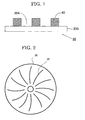
- FIG. 1 is a schematic partial cross-sectional view of a magnetic transfer master carrier 20.
- FIG. 2 is a top view of the magnetic transfer master carrier 20.
- the magnetic transfer master carrier 20 has a first base material 200 and magnetic convex portions 40.
- the material for the first base material 200 is not particularly limited and can be appropriately selected depending on the purpose. Examples thereof include known materials such as glass, synthetic resins (e.g., polycarbonates), metals (e.g., nickel and aluminum), silicon and carbon.
- the shape of the first base material 200 is not particularly limited and can be appropriately selected depending on the purpose.
- the magnetic transfer master carrier 20 shown in FIG. 2 has a disc shape.
- the thickness of the first base material 200 is not particularly limited and can be appropriately selected depending on the purpose.
- the first base material 200 preferably has a thickness of 0.05 mm to 1 mm, more preferably 0.1 mm to 0.5 mm.
- the thickness thereof is preferably 0.1 mm to 0.3 mm.
- the magnetic convex portions 40 are arranged on the first base material 200 correspondingly to a pattern corresponding to information to be recorded on a magnetic recording medium.
- a plurality of magnetic convex portions 40 are arranged on the first base material 200.
- Concave portions 204 are formed among the magnetic convex portions 40.
- the bottom surfaces of the concave portions 204 i.e., the surface of the first base material 200) are not provided with magnetic portions.
- the information to be recorded on the magnetic recording medium is, for example, servo information used for performing tracking servo; e.g., servo signals and address information signals.
- servo information used for performing tracking servo; e.g., servo signals and address information signals.
- the magnetic convex portions 40 on the first base material 200 form a radially extending pattern 52 corresponding to a pattern of information to be recorded.
- the magnetic convex portions 40 are formed from a laminate prepared by laminating a magnetic layer on the first base material 200.
- the magnetic layer of the laminate is etched to remove unnecessary portions of the magnetic layer, whereby magnetic convex portions 40 are formed.
- the magnetic material for the magnetic convex portions 40 include Co, CoPtCr, CoCr, CoPtCrTa, CoPtCrNbTa, CoCrB, CoNi, Fe, FeCo, FePt, FeNi, CoNb, FeSiAl and FeTaN.
- the material for the magnetic convex portions 40 is alloys or compounds composed of at least one ferromagnetic metal selected from Fe, Co and Ni and at least one non-magnetic atom selected from Cr, Pt, Ru, Pd, Si, Ti, B, Ta and O.
- the magnetic convex portions 40 have magnetic anisotropy directed perpendicularly to a recording surface of the magnetic recording medium (perpendicular magnetic anisotropy).
- each magnetic convex portion 40 is preferably 10 nm to 200 nm, more preferably 20 nm to 150 nm, still more preferably 40 nm to 100 nm.
- the magnetic convex portion 40 When the thickness (height) of the magnetic convex portion 40 is less than 10 nm, the magnetic convex portion may not attract a sufficient amount of magnetic flux. Whereas when the thickness (height) thereof is more than 200 nm, the remaining magnetization of the magnetic convex portion is increased to prevent desired transfer. Also, in general, the thicker the magnetic convex portion 40, the higher the cost therefor. Thus, the above range of 40 nm to 100 nm is preferred.
- the magnetic convex portion 40 may be provided with, for example, an underlying layer, a protective layer and a lubricating layer.
- the underlying layer (not shown) is formed under the magnetic convex portion 40 (i.e., between the magnetic convex portion 40 and first base material 200).
- the material for the underlying layer include metals, alloys and compounds, each containing at least one selected from Pt, Ru, Pd, Co, Cr, Ni, W, Ta, Al, P, Si and Ti, with platinum group metals (e.g., Pt and Ru) and alloys thereof being preferred.
- the underlying layer may have a single- or multi-layer structure.
- the thickness of the underlying layer is preferably 1 nm to 30 nm, more preferably 3 nm to 10 nm.
- the protective layer (not shown) is formed on the magnetic convex portion 40.
- the protective layer is made, for example, diamond-like carbon.
- the thickness of the protective layer is generally 10 nm or less.
- a lubricating layer (not shown) made, for example, of a fluorine-based lubricant (e.g., PFPE) may be formed on the protective layer.
- a production method of a magnetic transfer master carrier includes an imprint resist layer-forming step, a resist pattern-forming step, and a magnetic convex portion-forming step.
- FIGs. 3A to 3E are explanatory views of steps of the production method of a magnetic transfer master carrier. With reference to FIGs. 3A to 3E , next will be described the production method of a magnetic transfer master carrier.
- the imprint resist layer-forming step is a step of forming an imprint resist layer 39 (see FIG. 3B ) on a surface of a laminate 5 (see FIG. 3A ) having a first base material 200 and a magnetic layer 4 on the first base material 200, which surface is a surface of the magnetic layer 4.
- the imprint resist layer 39 is made of at least one selected from a thermoplastic resin, a thermosetting resin and a photocurable resin.
- the imprint resist layer 39 is formed by applying an imprint resist composition liquid, which is prepared by dissolving the above resin and the like in a predetermined solvent, onto a surface of the first base material 200 by a known coating method such as spin coating.
- the thickness of the imprint resist layer is appropriately determined in consideration of, for example, the depth of each concave portion of a mold described below. In general, it is preferably 10 nm to 100 nm.
- the magnetic layer 4 on the first base material 200 is formed using a known technique such as sputtering.
- the thickness of the magnetic layer 4 is appropriately determined according to the height of the magnetic convex portion 40.
- the magnetic convex portion 40 having the underlying layer is formed.
- an underlying layer is formed between the first base material 200 and the magnetic layer 4 to form the laminate 5.
- a hard mask serving as a mask layer may be formed on the magnetic layer 4.
- the mask layer is appropriately formed in consideration of a method for etching the magnetic layer 4.
- the material for the mask layer include metals, alloys and compounds, each containing at least one selected from C, Cr, W, Ta, Si and Ti.
- the mask layer is formed by a known method such as CVD and sputtering.
- the thickness of the mask layer is appropriately determined in consideration of the height of a magnetic convex portion 40 to be formed and the thickness of the imprint resist layer 39.
- the resist pattern-forming step is a step of forming, on a surface of the magnetic layer 4, a resist pattern 6, following shapes of concave portions 35 of a mold 36, by pressing the concave portions 35 against the imprint resist layer 39, the mold having a second base material and the concave portions 35 formed by etching a surface of the second base material so as to correspond to a pattern of information to be recorded on a magnetic recording medium (see FIG. 3C ).
- the mold 36 is used for forming the resist pattern 6 in the imprint resist layer 39.
- the mold 36 has the second base material and the concave portions 35 formed by etching a surface of the second base material so as to correspond to a pattern of information.
- FIGs. 4A to 4F are explanatory views of a production method of the mold 36. With reference to FIGs. 4A to 4F , the production method of the mold 36 will next be described.
- a base material 30 i.e., the second base material for producing the mold 36 is provided.
- the material for the second base material 30 is not particularly limited and can be appropriately selected depending on the purpose. Examples thereof include PETs, PENs, polycarbonates, low-melting-point fluorine resins, PMMAs, silicon and quartz.
- the second base material 30 must be made of a translucent material.
- an electron-beam resist liquid is applied onto a surface of the second base material 30 by a known coating method (e.g., spin coating) to form an electron-beam resist layer 32. Thereafter, the thus-formed electron-beam resist layer 32 is baked (pre-baked).
- a known coating method e.g., spin coating
- the electron-beam resist layer 32 is exposed to light using an unillustrated electron beam exposure apparatus having a high-precision rotary stage or X-Y stage.
- the second base material 30 having thereon the electron-beam resist layer 32 is set on the stage of the unillustrated exposure apparatus. While the second base material 30 is being rotated, an electron beam modulated correspondingly to a servo signal is applied to the electron-beam resist layer 32, whereby a pattern corresponding to the servo signal is formed in the electron-beam resist layer 32.
- portions indicated by reference numeral 33 are exposed portions.
- the resist layer 32 is developed to remove the exposed portions 33, whereby a patterned resist layer 32 is formed on the second base material 30.
- baking post-baking is carried out for enhancing adhesion between the patterned resist layer 32 and the second base material 30.
- the second base material 30 is etched using the resist layer 32 as a mask. Specifically, the second base material 30 exposed to dent portions 34 (corresponding to the exposed portions of the resist layer 32) is etched to form concave portions 35. This etching is preferably carried out through anisotropic etching such as reactive ion etching (RIE).
- RIE reactive ion etching
- the resist layer 32 remaining on the second base material 30 is removed through, for example, ashing, if necessary.
- the remaining resist layer 32 may be removed using a removing liquid.
- a mold 36 is obtained which is used in a production method of a magnetic transfer master carrier.
- the concave portions 35 of the mold 36 are pressed against the imprint resist layer 39 formed on the magnetic layer 4 of the laminate 5.
- the concave portions 35 are filled with the imprint resist layer 39.
- the imprint resist layer 39 is made of photocurable resin
- the imprint resist layer 39 is cured by irradiating the imprint resist layer 39 with light emitted through the translucent mold 36 from the outside.
- the imprint resist layer 39 is made of thermosetting resin
- the imprint resist layer 39 is cured through heating with the mold 36 being pressed thereagainst.
- the imprint resist layer 39 is made of thermoplastic resin
- the imprint resist layer 39 is cured through cooling with the mold 36 being pressed thereagainst, since the imprint resist layer 39 is softened; i.e., increased in temperature, during pressing of the mold 36 thereagainst.
- the magnetic convex portion-forming step is a step in which the mold 36 is removed from the imprint resist layer 39 and then, surfaces of the magnetic layer 4 which have no resist pattern 6 are etched to form the magnetic convex portions 40 on the first base material 200 (see FIG. 3D ).
- the mold 36 is removed from the imprint resist layer 39 formed on the laminate 5 and then, surfaces of the magnetic layer 4 which have no resist pattern 6 are etched through, for example, Ar ion beam etching until the first base material 200 is exposed.
- the magnetic layer 4 is etched to remove unnecessary portions of the magnetic layer 4. After the unnecessary portions have been removed, the magnetic convex portions 40 are formed on the first base material 200.
- the resist pattern 6 remaining on the magnetic convex portions 40 is removed through, for example, ashing, if necessary (removing step, see FIG. 3E ).
- a magnetic transfer master carrier 20 is obtained.
- the magnetic transfer master carrier 20 may be washed.
- a protective layer, etc. may be appropriately formed on the magnetic convex portions 40 through a known technique such as sputtering.
- the resist pattern 6 can be easily formed in the imprint resist layer 39 formed on the magnetic layer 4 of the laminate 5.
- the thicknesses (heights) of magnetic convex portions 40 can be set as desired.
- the magnetic transfer master carrier having magnetic convex portions 40 with a large thickness can be produced without involving deformation of the magnetic convex portions 40.
- a magnetic transfer master carrier in which unnecessary magnetic portions do not exist between the magnetic convex portions 40. According to this production method, the magnetic convex portions 40 are easily formed, as intended, on the surface of the first base material 200 correspondingly to information to be recorded.
- the magnetic transfer master carrier-production method of the present invention is a particularly preferred production method of a magnetic transfer master carrier containing magnetic convex portions 40 having magnetic anisotropy directed perpendicularly to the recording surface of a magnetic recording medium.
- FIGs. 5A to 5C schematically illustrate the magnetic transfer method.
- the magnetic transfer method includes an initial magnetization step, a closely attaching step and a magnetic transfer step.
- the initial magnetization step is a step of initially magnetizing the perpendicular magnetic recording medium 10 (slave disc) by applying a DC magnetic field (Hi) to the perpendicular magnetic recording medium 10.
- the DC magnetic field (Hi) is applied to the perpendicular magnetic recording medium 10.
- the DC magnetic field (initializing magnetic field) (Hi) is applied to the surface (recording surface) of the perpendicular magnetic recording medium 10 in a perpendicular direction.
- the DC magnetic field (Hi) is applied using a predetermined magnetic field applying unit (not illustrated).
- the intensity of the DC magnetic field (Hi) is maintained equal to or higher than the coercive force Hc of the perpendicular magnetic recording medium 10.
- FIG. 6 illustrates the direction of magnetization of a magnetic layer of the initially magnetized perpendicular magnetic recording medium.
- the magnetic layer of the initially magnetized perpendicular magnetic recording medium 10 is initially magnetized unidirectionally and perpendicularly to the surface of the perpendicular magnetic recording medium (disc) 10. Note that arrows indicated by Pi in FIG. 6 correspond to the direction in which the magnetic layer is magnetized.
- the closely attaching step is a step of closely attaching the magnetic transfer master carrier (master disc) 20 to the initially magnetized perpendicular magnetic recording medium 10.
- the initially magnetized perpendicular magnetic recording medium 10 is superposed on and closely attached to the magnetic transfer master carrier 20.
- the magnetic convex portions 40 formed on the surface of the magnetic transfer master carrier 20 are closely attached to the perpendicular magnetic recording medium 10.
- the magnetic transfer master carrier 20 is closely attached to the perpendicular magnetic recording medium 10 through application of a predetermined pressing force.
- the perpendicular magnetic recording medium 10 may be subjected to a cleaning process (e.g., burnishing) in which minute protrusions or attached powdery dust on its surface is removed using a grind head, a polisher or the like.
- a cleaning process e.g., burnishing
- the magnetic transfer master carrier 20 is closely attached only to one surface of the perpendicular magnetic recording medium 10 in the closely attaching step.
- magnetic transfer master carriers 20 may be closely attached to the surfaces.
- the magnetic transfer step is a step of recording, on the perpendicular magnetic recording medium 10, information based on the magnetic transfer master carrier 20 by applying a recording magnetic field (Hd) whose direction is opposite to that of the initializing magnetic field (Hi) to the perpendicular magnetic recording medium 10 and the magnetic transfer master carrier 20 that have been closely attached to each other.
- Hd recording magnetic field
- Hi initializing magnetic field
- the magnetic field (Hd), whose direction is opposite to that of the initializing magnetic field (Hi), is applied using a predetermined magnetic field applying unit (not illustrated) to the perpendicular magnetic recording medium 10 and the magnetic transfer master carrier 20 that have been closely attached to each other.
- FIG. 7 is a cross-sectional explanatory view of the perpendicular magnetic recording medium 10 and the magnetic transfer master carrier 20 at the magnetic transfer step.
- a magnetic flux G generated from the magnetic field (Hd) enters the magnetic transfer master carrier 20 and then is absorbed in the magnetic convex portions 40 of the magnetic transfer master carrier 20.
- portions of the magnetic layer contained in the perpendicular magnetic recording medium 10 which correspond to the magnetic convex portions 40 undergo inversion of magnetization for information, recording. Meanwhile, those corresponding to the concave portions 204 do not undergo inversion of magnetization.
- FIG. 8 illustrates the direction of magnetization of a magnetic layer of the perpendicular magnetic recording medium obtained after the magnetic transfer step.
- information e.g., servo signals
- FIG. 8 information (e.g., servo signals) is recorded on a magnetic layer of the perpendicular magnetic recording medium 10 in the form of recording magnetization Pd whose direction is opposite to that of the initializing magnetization Pi.
- the recording magnetic field (Hd) is appropriately determined depending on the purpose. In general, preferred is a magnetic field whose intensity is 40% to 130% the coercive force (Hc) of a magnetic layer of the perpendicular magnetic recording medium 10. More preferred is a magnetic field whose intensity is 50% to 120% the coercive force (Hc) of a magnetic layer of the perpendicular magnetic recording medium 10.
- An electron-beam resist was applied onto an Si wafer with a diameter of 20.32 cm (8 inch) (second base material 30) through spin coating so as to have a thickness of 100 nm. Thereafter, the resist applied on the second base material 30 was irradiated with an electron beam modulated correspondingly to, for example, a servo signal using a rotary electron beam exposure apparatus. Then, the resist was developed to remove unexposed portions, whereby the resist pattern of interest was formed on the second base material 30.
- the second base material 30 was subjected to a reactive etching treatment to etch portions having no resist (i.e., non-masked portions), whereby concave portions 35 were formed. After this etching treatment, the resist remaining on the second base material 30 was washed/removed with a solvent. Then, the second base material 30 was dried to produce a mold 36 used for producing a magnetic transfer master carrier.
- a Ta underlying layer (thickness: 10 nm) was formed on a (silicon) first base material 200 through sputtering. Then, an Ru underlying layer (thickness: 10 nm) was formed on the Ta underlying layer through sputtering.
- the conditions under which the sputtering was performed were as follows.
- a magnetic layer 4 (thickness: 40 nm) made of CoPt was formed on the underlying layer through sputtering.
- the conditions under which the magnetic layer 4 was formed were as follows.
- An imprint resist composition liquid (novolac resin) was applied onto the magnetic layer 4 of the above-obtained laminate 5 through spin coating so as to have a thickness of 25 nm, whereby an imprint resist layer 39 was formed.
- the concave portions 35 of the mold 36 were pressed against the thus-formed imprint resist layer 39.
- the mold 36 was applied to the imprint resist layer at a pressing force of 3 MPa for 10 sec under heating at 120°C, followed by curing of the resist.
- the mold 36 was removed from the imprint resist layer 39 to obtain a resist pattern (height: 100 nm) in the magnetic layer 4 of the laminate 5, which pattern was made of the imprint resist layer 39.
- the resist pattern was subjected to O 2 RIE to remove the resist remaining on imprint portions (concave portions).
- the magnetic layer 4 was etched with an Ar ion beam under the following conditions. As a result of this etching, magnetic convex portions 40 were formed on the first base material 200.
- the first base material 200 on which the magnetic convex portions 40 have been formed was washed and dried to produce a magnetic transfer master carrier.
- the produced perpendicular magnetic recording medium had, in sequence, a soft magnetic layer, a first non-magnetic orientation layer, a second non-magnetic orientation layer, a magnetic layer, a protective layer and a lubricating layer.
- the soft magnetic layer, the first non-magnetic orientation layer, the second non-magnetic orientation layer, the magnetic layer and the protective layer were formed through sputtering, and the lubricating layer was formed by a dip method.
- the soft magnetic layer was made of CoZrNb so as to have a thickness of 100 nm.
- the glass substrate was discharged at a DC power of 1,500 W with being placed so as to face a CoZrNb target.
- the first non-magnetic orientation layer was made of Ti so as to have a thickness of 5 nm.
- the glass substrate on which the soft magnetic layer has been formed was discharged at a DC power of 1,000 W with being placed so as to face a Ti target.
- the second non-magnetic orientation layer was made of Ru so as to have a thickness of 6 nm.
- the glass substrate over which the first non-magnetic orientation layer has been formed was discharged at a DC power of 900 W with being placed so as to face an Ru target.
- the magnetic layer was made of CoCrPtO so as to have a thickness of 18 nm.
- the glass substrate over which the second non-magnetic orientation layer has been formed was discharged at a DC power of 290 W with being placed so as to face a CoCrPtO target.
- the protective layer was made of C so as to have a thickness of 4 nm.
- the glass substrate over which the magnetic layer has been formed was discharged at a DC power of 1,000 W with being placed so as to face a C target.
- the lubricating layer was made of a PFPE lubricant so as to have a thickness of 2 nm.
- the perpendicular magnetic recording medium was found to have a coercive force of 334 kA/m (4.2 kOe).
- the perpendicular magnetic recording medium 10 was initially magnetized by applying a DC magnetic field (Hi) having an intensity of 10 kOe thereto.
- the above-produced magnetic transfer master carrier was closely attached to the initially magnetized perpendicular magnetic recording medium at a pressure of 9 kg/cm 2 .
- a recording magnetic field was applied to the perpendicular magnetic recording medium and the magnetic transfer master carrier that have been closely attached.
- the intensity of the recording magnetic field was 3.4 kOe.
- the thus-produced magnetic transfer master carrier was evaluated as follows.
- the patterned magnetic convex portions were evaluated for uniformity of their widths using an AFM (Dimension 5000, product of Nihon Veeco Co.). Specifically, almost equally-spaced 16 sites in a circle with a radius of 15 mm were measured to obtain data relating to the concavo-convex pattern; i.e., widths of the magnetic convex portions at heights 80% the heights of the portions, and dimensions of side surfaces of the magnetic convex portions. The standard deviations of the widths and dimensions were calculated to evaluate variation in them. Note that each of the sites had an area of 1 ⁇ m ⁇ 1 ⁇ m. The results are shown in Table 1.
- An electron-beam resist was applied onto a disc-shaped Si substrate with a diameter of 20.32 cm (8 inch) through spin coating so as to have a thickness of 100 nm. Thereafter, the resist applied on the Si substrate was irradiated with an electron beam modulated correspondingly to, for example, a servo signal using a rotary electron beam exposure apparatus. Then, the resist was developed to remove unexposed portions, whereby the resist pattern of interest was formed on the substrate.
- the Si substrate was subjected to a reactive etching treatment to etch portions having no resist (i.e., non-masked portions), whereby concave portions were formed.
- the resist remaining on the Si substrate was washed/removed with a solvent. Then, the substrate was dried to produce an original master used for producing a magnetic transfer master carrier.
- Ni thin film was formed through sputtering on a concavo-convex pattern of the above-produced original master. Subsequently, Ni plating (electrodeposition) was performed using the original master as an original plate, to thereby form an Ni layer. Thereafter, the Ni layer was removed from the original plate, followed by washing, whereby an Ni substrate was obtained.
- the thus-obtained Ni substrate had a concavo-convex surface.
- the magnetic transfer mold structure of Example 1 was equal to that of Comparative Example 1 in terms of processing accuracy of their convex portions (i.e., 13 nm vs. 11 nm). Nevertheless, the magnetic transfer mold structure of Example 1 was found to exhibit better (or higher) servo signal quality as compared with that of Comparative Example 1. Presumably, the reason for this is as follows. Specifically, in Comparative Example 1, the line widths of the convex portions were larger since the magnetic layer was formed after formation of a concavo-convex pattern; and the magnetic layer was formed not only the convex portions but also the concave portions.
Landscapes
- Engineering & Computer Science (AREA)
- Chemical & Material Sciences (AREA)
- Nanotechnology (AREA)
- Physics & Mathematics (AREA)
- Mathematical Physics (AREA)
- Theoretical Computer Science (AREA)
- Crystallography & Structural Chemistry (AREA)
- Manufacturing Of Magnetic Record Carriers (AREA)
- Magnetic Record Carriers (AREA)
Abstract
A production method of a magnetic transfer master carrier, the method including forming an imprint resist layer on a surface of a magnetic layer of a laminate which includes a first base material and the magnetic layer laminated thereon; forming a resist pattern, following shapes of concave portions of a mold, on the surface of the magnetic layer by pressing the concave portions against the imprint resist layer; and forming magnetic convex portions on the first base material by removing the mold from the imprint resist layer and then etching a surface of the magnetic layer which surface has no resist pattern, wherein the mold includes a second base material and the concave portions formed by etching a surface of the second base material so as to correspond to a pattern of information to be recorded on a magnetic recording medium.


Description
- The present invention relates to a production method of a magnetic transfer master carrier used for magnetically transferring information onto a magnetic recording medium; a magnetic transfer master carrier obtained by the production method; a magnetic transfer method using the magnetic transfer master carrier; and a magnetic recording medium obtained by the magnetic transfer method.
- Magnetic recording media record, as a so-called preformat, servo information used for tracking servo. The servo information is recorded on magnetic recording media using, for example, a master carrier. Such a master carrier has patterned magnetic portions formed correspondingly to a pattern of the servo information. When a recording magnetic field is applied to magnetic recording media with being closely attached to the magnetic potions of the master carrier, the magnetic recording media are magnetized based on the pattern of the magnetic portions. As a result, the servo information is recorded on the magnetic recording media at one time.
- One master carrier has a surface with convex portions on which top surfaces a magnetic layer is laid, as described in Japanese Patent Application Laid-Open (JP-A) No.
2001-256644 - Also,
JP-A No. 2000-195048 - In the master carrier production method described in
JP-A No. 2000-195048 - However, the above-described method, in which a resist pattern is formed through light exposure using a photomask, decreases in patterning accuracy as compared with the electron beam writing method, which is problematic.
- Also, when information to be recorded on magnetic recording media is servo information, the servo information must be recorded on the entire magnetic recording medium and the formed patterns must be different one another. Thus, the method in which a photomask is used as described in
JP-A No. 2000-195048 - Also, in the master carrier disclosed in
JP-A No. 2001-256644 - However, the magnetic layer of this master carrier is formed through, for example, sputtering on convex portions which have previously been formed as part of the base material. Thus, formation of a thick magnetic layer poses a problem in that processing accuracy thereof degrades; e.g., the widths of the convex portions become large.
- Under such circumstances, demand has arisen for a production method of a magnetic transfer master carrier (a magnetic transfer master carrier-production method) which method can produce, at good processing accuracy, a magnetic transfer master carrier capable of readily performing magnetic transfer of, for example, servo information.
- The present invention solves the above-described existing problems and aims to provide the following objects. That is, an object of the present invention is to provide a magnetic transfer master carrier-production method which exhibits good processing accuracy and which is reduced in production time, cost, etc.; a magnetic transfer master carrier obtained by the magnetic transfer master carrier-production method; a magnetic transfer method using the magnetic transfer master carrier; and a magnetic recording medium obtained by the magnetic transfer method.
- Means for solving the problems pertinent in the art are as follows.
- < 1 > A production method of a magnetic transfer master carrier, the production method including:
- forming an imprint resist layer on a surface of a magnetic layer of a laminate which includes a first base material and the magnetic layer laminated on the first base material,
- forming a resist pattern, following shapes of concave portions of a mold, on the surface of the magnetic layer by pressing the concave portions against the imprint resist layer, and
- forming magnetic convex portions on the first base material by removing the mold from the imprint resist layer and then etching a surface of the magnetic layer which surface has no resist pattern,
- wherein the mold includes a second base material and the concave portions formed by etching a surface of the second base material so as to correspond to a pattern of information to be recorded on a magnetic recording medium, and
- wherein the magnetic transfer master carrier includes the first base material and the magnetic convex portions made of a magnetic material, the magnetic convex portions being arranged on the first base material correspondingly to the pattern of the information, and forms a magnetic field pattern by absorbing a magnetic flux in the magnetic convex portions when a magnetic field is applied to the magnetic transfer master carrier.
- < 2 > The production method according to < 1 > above, wherein the laminate further includes an underlying layer between the first base material and the magnetic layer.
- < 3 > The production method according to < 1 > or < 2 > above, wherein the magnetic layer has perpendicular magnetic anisotropy.
- < 4 > A magnetic transfer master carrier including:
- a first base material, and
- magnetic convex portions made of a magnetic material, the magnetic convex portions being arranged on the first base material correspondingly to a pattern of information to be recorded on a magnetic recording medium,
- wherein the magnetic transfer master carrier forms a magnetic field pattern by absorbing a magnetic flux in the magnetic convex portions when a magnetic field is applied to the magnetic transfer master carrier, and is obtained by the production method according to any one of < 1 > to < 3 > above.
- < 5 > A magnetic transfer method including:
- initially magnetizing a perpendicular magnetic recording medium by applying a magnetic field thereto,
- closely attaching the magnetic transfer master carrier according to < 4 > above to the initially magnetized perpendicular magnetic recording medium, and
- magnetically transferring information to the perpendicular magnetic recording medium by applying thereto a magnetic field whose direction is opposite to a direction of the magnetic field applied in the initial magnetization, with the perpendicular magnetic recording medium and the magnetic transfer master carrier being closely attached to each other, so that the information is recorded on the perpendicular magnetic recording medium.
- < 6 > A magnetic recording medium obtained by the magnetic transfer method according to < 5 > above.
- The present invention can provide a magnetic transfer master carrier-production method which exhibits good processing accuracy and which is reduced in production time, cost, etc.; a magnetic transfer master carrier obtained by the magnetic transfer master carrier-production method; a magnetic transfer method using the magnetic transfer master carrier; and a magnetic recording medium obtained by the magnetic transfer method. These can solve the above-described existing problems.
-
-
FIG. 1 is a schematic partial cross-sectional view of a magnetic transfer master carrier. -
FIG. 2 is a top view of the magnetic transfer master carrier. -
FIG. 3A is an explanatory view of a step of a production method of a magnetic transfer master carrier. -
FIG. 3B is an explanatory view of a step of a production method of a magnetic transfer master carrier. -
FIG. 3C is an explanatory view of a step of a production method of a magnetic transfer master carrier. -
FIG. 3D is an explanatory view of a step of a production method of a magnetic transfer master carrier. -
FIG. 3E is an explanatory view of a step of a production method of a magnetic transfer master carrier. -
FIG. 4A is an explanatory view of a step of a production method of a mold. -
FIG. 4B is an explanatory view of a step of a production method of a mold. -
FIG. 4C is an explanatory view of a step of a production method of a mold. -
FIG. 4D is an explanatory view of a step of a production method of a mold. -
FIG. 4E is an explanatory view of a step of a production method of a mold. -
FIG. 4F is an explanatory view of a step of a production method of a mold. -
FIG. 5A schematically illustrates a magnetic transfer method. -
FIG. 5B schematically illustrates a magnetic transfer method. -
FIG. 5C schematically illustrates a magnetic transfer method. -
FIG. 6 illustrates the direction of magnetization of a magnetic layer of a perpendicular magnetic recording medium having undergone initial magnetization. -
FIG. 7 is a cross-sectional explanatory view of a perpendicular magnetic recording medium and a magnetic transfer master carrier at a magnetic transfer step. -
FIG. 8 illustrates the direction of magnetization of a magnetic layer of a perpendicular magnetic recording medium obtained after a magnetic transfer step. - With reference to
FIGs. 1 and 2 , first will be described a magnetic transfer master carrier obtained by a production method of the present invention which is for a magnetic transfer master carrier. -
FIG. 1 is a schematic partial cross-sectional view of a magnetictransfer master carrier 20.FIG. 2 is a top view of the magnetictransfer master carrier 20. As shown inFIG. 1 , the magnetictransfer master carrier 20 has afirst base material 200 and magneticconvex portions 40. - The material for the
first base material 200 is not particularly limited and can be appropriately selected depending on the purpose. Examples thereof include known materials such as glass, synthetic resins (e.g., polycarbonates), metals (e.g., nickel and aluminum), silicon and carbon. - The shape of the
first base material 200 is not particularly limited and can be appropriately selected depending on the purpose. The magnetictransfer master carrier 20 shown inFIG. 2 has a disc shape. - The thickness of the
first base material 200 is not particularly limited and can be appropriately selected depending on the purpose. Thefirst base material 200 preferably has a thickness of 0.05 mm to 1 mm, more preferably 0.1 mm to 0.5 mm. - Notably, when the
first base material 200 is made of Ni, the thickness thereof is preferably 0.1 mm to 0.3 mm. - The magnetic
convex portions 40 are arranged on thefirst base material 200 correspondingly to a pattern corresponding to information to be recorded on a magnetic recording medium. A plurality of magneticconvex portions 40 are arranged on thefirst base material 200.Concave portions 204 are formed among the magneticconvex portions 40. The bottom surfaces of the concave portions 204 (i.e., the surface of the first base material 200) are not provided with magnetic portions. - The information to be recorded on the magnetic recording medium is, for example, servo information used for performing tracking servo; e.g., servo signals and address information signals. As shown in
FIG. 2 , the magneticconvex portions 40 on thefirst base material 200 form aradially extending pattern 52 corresponding to a pattern of information to be recorded. - As described below, the magnetic
convex portions 40 are formed from a laminate prepared by laminating a magnetic layer on thefirst base material 200. The magnetic layer of the laminate is etched to remove unnecessary portions of the magnetic layer, whereby magneticconvex portions 40 are formed. - The magnetic material for the magnetic
convex portions 40 include Co, CoPtCr, CoCr, CoPtCrTa, CoPtCrNbTa, CoCrB, CoNi, Fe, FeCo, FePt, FeNi, CoNb, FeSiAl and FeTaN. - Notably, in the case of a magnetic transfer master carrier used for recording information on a perpendicular magnetic recording medium, the material for the magnetic
convex portions 40 is alloys or compounds composed of at least one ferromagnetic metal selected from Fe, Co and Ni and at least one non-magnetic atom selected from Cr, Pt, Ru, Pd, Si, Ti, B, Ta and O. - In this case, the magnetic
convex portions 40 have magnetic anisotropy directed perpendicularly to a recording surface of the magnetic recording medium (perpendicular magnetic anisotropy). - The thickness (height) of each magnetic
convex portion 40 is preferably 10 nm to 200 nm, more preferably 20 nm to 150 nm, still more preferably 40 nm to 100 nm. - When the thickness (height) of the magnetic
convex portion 40 is less than 10 nm, the magnetic convex portion may not attract a sufficient amount of magnetic flux. Whereas when the thickness (height) thereof is more than 200 nm, the remaining magnetization of the magnetic convex portion is increased to prevent desired transfer. Also, in general, the thicker the magneticconvex portion 40, the higher the cost therefor. Thus, the above range of 40 nm to 100 nm is preferred. - If necessary, the magnetic
convex portion 40 may be provided with, for example, an underlying layer, a protective layer and a lubricating layer. - The underlying layer (not shown) is formed under the magnetic convex portion 40 (i.e., between the magnetic
convex portion 40 and first base material 200). Examples of the material for the underlying layer include metals, alloys and compounds, each containing at least one selected from Pt, Ru, Pd, Co, Cr, Ni, W, Ta, Al, P, Si and Ti, with platinum group metals (e.g., Pt and Ru) and alloys thereof being preferred. The underlying layer may have a single- or multi-layer structure. The thickness of the underlying layer is preferably 1 nm to 30 nm, more preferably 3 nm to 10 nm. - The protective layer (not shown) is formed on the magnetic
convex portion 40. The protective layer is made, for example, diamond-like carbon. The thickness of the protective layer is generally 10 nm or less. Furthermore, a lubricating layer (not shown) made, for example, of a fluorine-based lubricant (e.g., PFPE) may be formed on the protective layer. - A production method of a magnetic transfer master carrier according to the present embodiment includes an imprint resist layer-forming step, a resist pattern-forming step, and a magnetic convex portion-forming step.
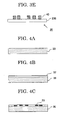
FIGs. 3A to 3E are explanatory views of steps of the production method of a magnetic transfer master carrier. With reference toFIGs. 3A to 3E , next will be described the production method of a magnetic transfer master carrier. - The imprint resist layer-forming step is a step of forming an imprint resist layer 39 (see
FIG. 3B ) on a surface of a laminate 5 (seeFIG. 3A ) having afirst base material 200 and amagnetic layer 4 on thefirst base material 200, which surface is a surface of themagnetic layer 4. - The imprint resist
layer 39 is made of at least one selected from a thermoplastic resin, a thermosetting resin and a photocurable resin. - The imprint resist
layer 39 is formed by applying an imprint resist composition liquid, which is prepared by dissolving the above resin and the like in a predetermined solvent, onto a surface of thefirst base material 200 by a known coating method such as spin coating. - The thickness of the imprint resist layer is appropriately determined in consideration of, for example, the depth of each concave portion of a mold described below. In general, it is preferably 10 nm to 100 nm.
- In the
laminate 5, themagnetic layer 4 on thefirst base material 200 is formed using a known technique such as sputtering. The thickness of themagnetic layer 4 is appropriately determined according to the height of the magneticconvex portion 40. - Notably, in another embodiment, the magnetic
convex portion 40 having the underlying layer is formed. In this case, an underlying layer is formed between thefirst base material 200 and themagnetic layer 4 to form thelaminate 5. - Further, in still another embodiment, a hard mask serving as a mask layer may be formed on the
magnetic layer 4. The mask layer is appropriately formed in consideration of a method for etching themagnetic layer 4. Examples of the material for the mask layer include metals, alloys and compounds, each containing at least one selected from C, Cr, W, Ta, Si and Ti. The mask layer is formed by a known method such as CVD and sputtering. The thickness of the mask layer is appropriately determined in consideration of the height of a magneticconvex portion 40 to be formed and the thickness of the imprint resistlayer 39. - The resist pattern-forming step is a step of forming, on a surface of the
magnetic layer 4, a resistpattern 6, following shapes ofconcave portions 35 of amold 36, by pressing theconcave portions 35 against the imprint resistlayer 39, the mold having a second base material and theconcave portions 35 formed by etching a surface of the second base material so as to correspond to a pattern of information to be recorded on a magnetic recording medium (seeFIG. 3C ). - The
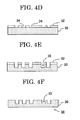
mold 36 is used for forming the resistpattern 6 in the imprint resistlayer 39. As described above, themold 36 has the second base material and theconcave portions 35 formed by etching a surface of the second base material so as to correspond to a pattern of information.FIGs. 4A to 4F are explanatory views of a production method of themold 36. With reference toFIGs. 4A to 4F , the production method of themold 36 will next be described. - As shown in
FIG. 4A , first, a base material 30 (i.e., the second base material) for producing themold 36 is provided. - The material for the
second base material 30 is not particularly limited and can be appropriately selected depending on the purpose. Examples thereof include PETs, PENs, polycarbonates, low-melting-point fluorine resins, PMMAs, silicon and quartz. - Notably, when an imprint resist
layer 39 made of photocurable resin is used in the imprint resist layer-forming step, thesecond base material 30 must be made of a translucent material. - Next, as shown in
FIG. 4B , an electron-beam resist liquid is applied onto a surface of thesecond base material 30 by a known coating method (e.g., spin coating) to form an electron-beam resistlayer 32. Thereafter, the thus-formed electron-beam resistlayer 32 is baked (pre-baked). - Next, as shown in
FIG. 4C , the electron-beam resistlayer 32 is exposed to light using an unillustrated electron beam exposure apparatus having a high-precision rotary stage or X-Y stage. Specifically, thesecond base material 30 having thereon the electron-beam resistlayer 32 is set on the stage of the unillustrated exposure apparatus. While thesecond base material 30 is being rotated, an electron beam modulated correspondingly to a servo signal is applied to the electron-beam resistlayer 32, whereby a pattern corresponding to the servo signal is formed in the electron-beam resistlayer 32. InFIG. 4C , portions indicated byreference numeral 33 are exposed portions. - Next, as shown in
FIG. 4D , the resistlayer 32 is developed to remove the exposedportions 33, whereby a patterned resistlayer 32 is formed on thesecond base material 30. After development, baking (post-baking) is carried out for enhancing adhesion between the patterned resistlayer 32 and thesecond base material 30. - Next, as shown in
FIG. 4E , thesecond base material 30 is etched using the resistlayer 32 as a mask. Specifically, thesecond base material 30 exposed to dent portions 34 (corresponding to the exposed portions of the resist layer 32) is etched to formconcave portions 35. This etching is preferably carried out through anisotropic etching such as reactive ion etching (RIE). - Next, as shown in
FIG. 4F , the resistlayer 32 remaining on thesecond base material 30 is removed through, for example, ashing, if necessary. Alternatively, the remaining resistlayer 32 may be removed using a removing liquid. - After removal of the resist
layer 32, amold 36 is obtained which is used in a production method of a magnetic transfer master carrier. - Referring again to
FIG. 3C , the following description will be given. As shown inFIG. 3C , theconcave portions 35 of themold 36 are pressed against the imprint resistlayer 39 formed on themagnetic layer 4 of thelaminate 5. When theconcave portions 35 of themold 36 are pressed against the imprint resistlayer 39, theconcave portions 35 are filled with the imprint resistlayer 39. As a result, there is formed a resistpattern 6 made of the imprint resistlayer 39 which pattern corresponds to theconcave portions 35. - When the imprint resist
layer 39 is made of photocurable resin, the imprint resistlayer 39 is cured by irradiating the imprint resistlayer 39 with light emitted through thetranslucent mold 36 from the outside. - When the imprint resist
layer 39 is made of thermosetting resin, the imprint resistlayer 39 is cured through heating with themold 36 being pressed thereagainst. - When the imprint resist
layer 39 is made of thermoplastic resin, the imprint resistlayer 39 is cured through cooling with themold 36 being pressed thereagainst, since the imprint resistlayer 39 is softened; i.e., increased in temperature, during pressing of themold 36 thereagainst. - The magnetic convex portion-forming step is a step in which the
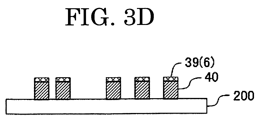
mold 36 is removed from the imprint resistlayer 39 and then, surfaces of themagnetic layer 4 which have no resistpattern 6 are etched to form the magneticconvex portions 40 on the first base material 200 (seeFIG. 3D ). - As shown in
FIG. 3D , themold 36 is removed from the imprint resistlayer 39 formed on thelaminate 5 and then, surfaces of themagnetic layer 4 which have no resistpattern 6 are etched through, for example, Ar ion beam etching until thefirst base material 200 is exposed. In other words, themagnetic layer 4 is etched to remove unnecessary portions of themagnetic layer 4. After the unnecessary portions have been removed, the magneticconvex portions 40 are formed on thefirst base material 200. - Thereafter, the resist
pattern 6 remaining on the magneticconvex portions 40 is removed through, for example, ashing, if necessary (removing step, seeFIG. 3E ). Through the above procedure, a magnetictransfer master carrier 20 is obtained. - If necessary, the magnetic
transfer master carrier 20 may be washed. Also, a protective layer, etc. may be appropriately formed on the magneticconvex portions 40 through a known technique such as sputtering. - In the magnetic transfer master carrier-production method of the present invention, by using the
mold 36, the resistpattern 6 can be easily formed in the imprint resistlayer 39 formed on themagnetic layer 4 of thelaminate 5. - Also, in the magnetic transfer master carrier-production method of the present invention, the thicknesses (heights) of magnetic
convex portions 40 can be set as desired. For example, the magnetic transfer master carrier having magneticconvex portions 40 with a large thickness can be produced without involving deformation of the magneticconvex portions 40. - Also, in the magnetic transfer master carrier-production method of the present invention, a magnetic transfer master carrier can be produced in which unnecessary magnetic portions do not exist between the magnetic
convex portions 40. According to this production method, the magneticconvex portions 40 are easily formed, as intended, on the surface of thefirst base material 200 correspondingly to information to be recorded. - Also, in the magnetic transfer master carrier-production method of the present invention, a magnetic transfer master carrier whose magnetic
convex portions 40 are formed on an underlying layer can be easily produced. The underlying layer can control orientation of crystals contained in the magneticconvex portions 40. Thus, the magnetic transfer master carrier-production method of the present invention is a particularly preferred production method of a magnetic transfer master carrier containing magneticconvex portions 40 having magnetic anisotropy directed perpendicularly to the recording surface of a magnetic recording medium. - Next will be described a method for recording (or magnetically transferring) information onto a magnetic recording medium (perpendicular magnetic recording medium) using a magnetic transfer master carrier obtained by the production method of a magnetic transfer master carrier.
-
FIGs. 5A to 5C schematically illustrate the magnetic transfer method. The magnetic transfer method includes an initial magnetization step, a closely attaching step and a magnetic transfer step. - The initial magnetization step is a step of initially magnetizing the perpendicular magnetic recording medium 10 (slave disc) by applying a DC magnetic field (Hi) to the perpendicular
magnetic recording medium 10. - As shown in
FIG. 5A , in the initial magnetization step, the DC magnetic field (Hi) is applied to the perpendicularmagnetic recording medium 10. The DC magnetic field (initializing magnetic field) (Hi) is applied to the surface (recording surface) of the perpendicularmagnetic recording medium 10 in a perpendicular direction. The DC magnetic field (Hi) is applied using a predetermined magnetic field applying unit (not illustrated). The intensity of the DC magnetic field (Hi) is maintained equal to or higher than the coercive force Hc of the perpendicularmagnetic recording medium 10. -
FIG. 6 illustrates the direction of magnetization of a magnetic layer of the initially magnetized perpendicular magnetic recording medium. As shown inFIG. 6 , the magnetic layer of the initially magnetized perpendicularmagnetic recording medium 10 is initially magnetized unidirectionally and perpendicularly to the surface of the perpendicular magnetic recording medium (disc) 10. Note that arrows indicated by Pi inFIG. 6 correspond to the direction in which the magnetic layer is magnetized. - The closely attaching step is a step of closely attaching the magnetic transfer master carrier (master disc) 20 to the initially magnetized perpendicular
magnetic recording medium 10. - As shown in
FIG. 5B , the initially magnetized perpendicularmagnetic recording medium 10 is superposed on and closely attached to the magnetictransfer master carrier 20. - In the closely attaching step, the magnetic
convex portions 40 formed on the surface of the magnetictransfer master carrier 20 are closely attached to the perpendicularmagnetic recording medium 10. The magnetictransfer master carrier 20 is closely attached to the perpendicularmagnetic recording medium 10 through application of a predetermined pressing force. - If necessary, before the magnetic
transfer master carrier 20 is closely attached to the perpendicularmagnetic recording medium 10, the perpendicularmagnetic recording medium 10 may be subjected to a cleaning process (e.g., burnishing) in which minute protrusions or attached powdery dust on its surface is removed using a grind head, a polisher or the like. - In the present embodiment, as shown in
FIG. 5B , the magnetictransfer master carrier 20 is closely attached only to one surface of the perpendicularmagnetic recording medium 10 in the closely attaching step. Alternatively, in another embodiment, using a perpendicular magnetic recording medium (slave disc) having a magnetic layer on both surfaces, magnetictransfer master carriers 20 may be closely attached to the surfaces. - The magnetic transfer step is a step of recording, on the perpendicular
magnetic recording medium 10, information based on the magnetictransfer master carrier 20 by applying a recording magnetic field (Hd) whose direction is opposite to that of the initializing magnetic field (Hi) to the perpendicularmagnetic recording medium 10 and the magnetictransfer master carrier 20 that have been closely attached to each other. - As shown in
FIG. 5C , the magnetic field (Hd), whose direction is opposite to that of the initializing magnetic field (Hi), is applied using a predetermined magnetic field applying unit (not illustrated) to the perpendicularmagnetic recording medium 10 and the magnetictransfer master carrier 20 that have been closely attached to each other. -
FIG. 7 is a cross-sectional explanatory view of the perpendicularmagnetic recording medium 10 and the magnetictransfer master carrier 20 at the magnetic transfer step. As shown inFIG. 7 , when the recording magnetic field (Hd) is applied to the perpendicularmagnetic recording medium 10 and the magnetictransfer master carrier 20 that have been closely attached to each other, a magnetic flux G generated from the magnetic field (Hd) enters the magnetictransfer master carrier 20 and then is absorbed in the magneticconvex portions 40 of the magnetictransfer master carrier 20. - As a result, a strong magnetic field is generated in the magnetic
convex portions 40 of the magnetictransfer master carrier 20. Meanwhile, a magnetic field ofconcave portions 204 of the magnetic transfer master carrier 20-interspaces between the magnetic convex portions 40-is weaker than that of the magneticconvex portions 40. In this manner, a magnetic field pattern corresponding to information to be recorded is formed on the perpendicularmagnetic recording medium 10. - As a result, portions of the magnetic layer contained in the perpendicular
magnetic recording medium 10 which correspond to the magneticconvex portions 40 undergo inversion of magnetization for information, recording. Meanwhile, those corresponding to theconcave portions 204 do not undergo inversion of magnetization. -
FIG. 8 illustrates the direction of magnetization of a magnetic layer of the perpendicular magnetic recording medium obtained after the magnetic transfer step. As shown inFIG. 8 , information (e.g., servo signals) is recorded on a magnetic layer of the perpendicularmagnetic recording medium 10 in the form of recording magnetization Pd whose direction is opposite to that of the initializing magnetization Pi. - The recording magnetic field (Hd) is appropriately determined depending on the purpose. In general, preferred is a magnetic field whose intensity is 40% to 130% the coercive force (Hc) of a magnetic layer of the perpendicular
magnetic recording medium 10. More preferred is a magnetic field whose intensity is 50% to 120% the coercive force (Hc) of a magnetic layer of the perpendicularmagnetic recording medium 10. - The present invention will next be described by way of examples, which should not be construed as limiting the present invention thereto.
- An electron-beam resist was applied onto an Si wafer with a diameter of 20.32 cm (8 inch) (second base material 30) through spin coating so as to have a thickness of 100 nm. Thereafter, the resist applied on the
second base material 30 was irradiated with an electron beam modulated correspondingly to, for example, a servo signal using a rotary electron beam exposure apparatus. Then, the resist was developed to remove unexposed portions, whereby the resist pattern of interest was formed on thesecond base material 30. - Subsequently, using the above-formed patterned resist as a mask, the
second base material 30 was subjected to a reactive etching treatment to etch portions having no resist (i.e., non-masked portions), wherebyconcave portions 35 were formed. After this etching treatment, the resist remaining on thesecond base material 30 was washed/removed with a solvent. Then, thesecond base material 30 was dried to produce amold 36 used for producing a magnetic transfer master carrier. - A Ta underlying layer (thickness: 10 nm) was formed on a (silicon)
first base material 200 through sputtering. Then, an Ru underlying layer (thickness: 10 nm) was formed on the Ta underlying layer through sputtering. The conditions under which the sputtering was performed were as follows. -
- Target material: Ta
- Distance between target and first base material: 200 mm
- Pressure: 0.5 Pa
- DC power: 350 W
-
- Target material: Ru
- Distance between target and first base material: 200 mm
- Pressure: 0.3 Pa
- DC power: 300 W
- Thereafter, a magnetic layer 4 (thickness: 40 nm) made of CoPt was formed on the underlying layer through sputtering. The conditions under which the
magnetic layer 4 was formed were as follows. - Target material: Co80Pt20
- Distance between target and first base material: 200 mm
- Pressure: 0.1 Pa
- DC power: 1,000 W
- Through the above procedure, a
laminate 5 was obtained. - An imprint resist composition liquid (novolac resin) was applied onto the
magnetic layer 4 of the above-obtainedlaminate 5 through spin coating so as to have a thickness of 25 nm, whereby an imprint resistlayer 39 was formed. - The
concave portions 35 of themold 36 were pressed against the thus-formed imprint resistlayer 39. Themold 36 was applied to the imprint resist layer at a pressing force of 3 MPa for 10 sec under heating at 120°C, followed by curing of the resist. - Then, the
mold 36 was removed from the imprint resistlayer 39 to obtain a resist pattern (height: 100 nm) in themagnetic layer 4 of thelaminate 5, which pattern was made of the imprint resistlayer 39. The resist pattern was subjected to O2 RIE to remove the resist remaining on imprint portions (concave portions). - Using the resist pattern as a mask, the
magnetic layer 4 was etched with an Ar ion beam under the following conditions. As a result of this etching, magneticconvex portions 40 were formed on thefirst base material 200. - Thereafter, the resist pattern remaining on the magnetic
convex portions 40 was removed through O2 RIE. - Then, the
first base material 200 on which the magneticconvex portions 40 have been formed was washed and dried to produce a magnetic transfer master carrier. - The below-described layers were formed in the following manner on a glass substrate with a diameter of 6.35 cm (2.5 inch) to produce a perpendicular magnetic recording medium.
- Specifically, the produced perpendicular magnetic recording medium had, in sequence, a soft magnetic layer, a first non-magnetic orientation layer, a second non-magnetic orientation layer, a magnetic layer, a protective layer and a lubricating layer.
- Notably, the soft magnetic layer, the first non-magnetic orientation layer, the second non-magnetic orientation layer, the magnetic layer and the protective layer were formed through sputtering, and the lubricating layer was formed by a dip method.
- The soft magnetic layer was made of CoZrNb so as to have a thickness of 100 nm.
- Specifically, while an Ar gas was being fed into a chamber so that the gas pressure was adjusted to 0.6 Pa, the glass substrate was discharged at a DC power of 1,500 W with being placed so as to face a CoZrNb target.
- The first non-magnetic orientation layer was made of Ti so as to have a thickness of 5 nm.
- Specifically, while an Ar gas was being fed into a chamber so that the gas pressure was adjusted to 0.5 Pa, the glass substrate on which the soft magnetic layer has been formed was discharged at a DC power of 1,000 W with being placed so as to face a Ti target.
- The second non-magnetic orientation layer was made of Ru so as to have a thickness of 6 nm.
- Specifically, while an Ar gas was being fed into a chamber so that the gas pressure was adjusted to 0.8 Pa, the glass substrate over which the first non-magnetic orientation layer has been formed was discharged at a DC power of 900 W with being placed so as to face an Ru target.
- The magnetic layer was made of CoCrPtO so as to have a thickness of 18 nm.
- Specifically, while an Ar gas containing O2 (0.06%) was being fed into a chamber so that the gas pressure was adjusted to 14 Pa, the glass substrate over which the second non-magnetic orientation layer has been formed was discharged at a DC power of 290 W with being placed so as to face a CoCrPtO target.
- The protective layer was made of C so as to have a thickness of 4 nm.
- Specifically, while an Ar gas was being fed into a chamber so that the gas pressure was adjusted to 0.5 Pa, the glass substrate over which the magnetic layer has been formed was discharged at a DC power of 1,000 W with being placed so as to face a C target.
- The lubricating layer was made of a PFPE lubricant so as to have a thickness of 2 nm.
- The perpendicular magnetic recording medium was found to have a coercive force of 334 kA/m (4.2 kOe).
- The perpendicular
magnetic recording medium 10 was initially magnetized by applying a DC magnetic field (Hi) having an intensity of 10 kOe thereto. - The above-produced magnetic transfer master carrier was closely attached to the initially magnetized perpendicular magnetic recording medium at a pressure of 9 kg/cm2.
- A recording magnetic field was applied to the perpendicular magnetic recording medium and the magnetic transfer master carrier that have been closely attached. The intensity of the recording magnetic field was 3.4 kOe.
- Thereafter, application of the recording magnetic field was terminated and then, the magnetic transfer master carrier was separated from the perpendicular magnetic recording medium.
- The thus-produced magnetic transfer master carrier was evaluated as follows.
- The patterned magnetic convex portions were evaluated for uniformity of their widths using an AFM (Dimension 5000, product of Nihon Veeco Co.). Specifically, almost equally-spaced 16 sites in a circle with a radius of 15 mm were measured to obtain data relating to the concavo-convex pattern; i.e., widths of the magnetic convex portions at heights 80% the heights of the portions, and dimensions of side surfaces of the magnetic convex portions. The standard deviations of the widths and dimensions were calculated to evaluate variation in them. Note that each of the sites had an area of 1 µm × 1 µm. The results are shown in Table 1.
- There were evaluated qualities of servo signals recorded on the magnetic recording medium through magnetic transfer using the magnetic transfer master carrier. Specifically, reproduced outputs (track average amplitude (TAN) in a preamble area were detected in each sector within a circle of radius of 15 mm, and then the SNR of the outputs was calculated to evaluate servo signal quality. This evaluation was carried out using LS-90 (product of Kyodo Denshi Co.) and a GMR head (read width: 120 nm, and write width: 200 nm). The results are shown in Table 1.
- An electron-beam resist was applied onto a disc-shaped Si substrate with a diameter of 20.32 cm (8 inch) through spin coating so as to have a thickness of 100 nm. Thereafter, the resist applied on the Si substrate was irradiated with an electron beam modulated correspondingly to, for example, a servo signal using a rotary electron beam exposure apparatus. Then, the resist was developed to remove unexposed portions, whereby the resist pattern of interest was formed on the substrate.
- Subsequently, using the above-formed patterned resist as a mask, the Si substrate was subjected to a reactive etching treatment to etch portions having no resist (i.e., non-masked portions), whereby concave portions were formed. After this etching treatment, the resist remaining on the Si substrate was washed/removed with a solvent. Then, the substrate was dried to produce an original master used for producing a magnetic transfer master carrier.
- First, an Ni thin film was formed through sputtering on a concavo-convex pattern of the above-produced original master. Subsequently, Ni plating (electrodeposition) was performed using the original master as an original plate, to thereby form an Ni layer. Thereafter, the Ni layer was removed from the original plate, followed by washing, whereby an Ni substrate was obtained. The thus-obtained Ni substrate had a concavo-convex surface.
- Then, a Ta film (thickness: 5 nm), an Ru film (thickness: 5 nm) and a Co80Pt20 film (thickness: 40 nm) were sequentially formed through sputtering on the convex portions of the Ni substrate, to thereby produce a magnetic transfer master carrier of Comparative Example 1.
- Similar to Example 1, the magnetic transfer master carrier of Comparative Example 1 was evaluated according to
Evaluations 1 and 2. The results are shown in Table 1.Table 1 Width of convex portion at height 80% the height thereof (nm) Processing accuracy of convex portions: 3σ (nm) Servo signal quality: SNR (dB) Ex.1 67 13 14.3 Comp. Ex. 1 78 11 11.7 - As is clear from Table 1, the magnetic transfer mold structure of Example 1 was equal to that of Comparative Example 1 in terms of processing accuracy of their convex portions (i.e., 13 nm vs. 11 nm). Nevertheless, the magnetic transfer mold structure of Example 1 was found to exhibit better (or higher) servo signal quality as compared with that of Comparative Example 1. Presumably, the reason for this is as follows. Specifically, in Comparative Example 1, the line widths of the convex portions were larger since the magnetic layer was formed after formation of a concavo-convex pattern; and the magnetic layer was formed not only the convex portions but also the concave portions.
Claims (6)
- A production method of a magnetic transfer master carrier, the production method comprising:forming an imprint resist layer on a surface of a magnetic layer of a laminate which comprises a first base material and the magnetic layer laminated on the first base material,forming a resist pattern, following shapes of concave portions of a mold, on the surface of the magnetic layer by pressing the concave portions against the imprint resist layer, andforming magnetic convex portions on the first base material by removing the mold from the imprint resist layer and then etching a surface of the magnetic layer which surface has no resist pattern,wherein the mold comprises a second base material and the concave portions formed by etching a surface of the second base material so as to correspond to a pattern of information to be recorded on a magnetic recording medium, andwherein the magnetic transfer master carrier comprises the first base material and the magnetic convex portions made of a magnetic material, the magnetic convex portions being arranged on the first base material correspondingly to the pattern of the information, and forms a magnetic field pattern by absorbing a magnetic flux in the magnetic convex portions when a magnetic field is applied to the magnetic transfer master carrier.
- The production method according to claim 1, wherein the laminate further comprises an underlying layer between the first base material and the magnetic layer.
- The production method according to claim 1 or 2, wherein the magnetic layer has perpendicular magnetic anisotropy.
- A magnetic transfer master carrier comprising:a first base material, andmagnetic convex portions made of a magnetic material, the magnetic convex portions being arranged on the first base material correspondingly to a pattern of information to be recorded on a magnetic recording medium,wherein the magnetic transfer master carrier forms a magnetic field pattern by absorbing a magnetic flux in the magnetic convex portions when a magnetic field is applied to the magnetic transfer master carrier, and is obtained by the production method according to any one of claims 1 to 3.
- A magnetic transfer method comprising:initially magnetizing a perpendicular magnetic recording medium by applying a magnetic field thereto,closely attaching the magnetic transfer master carrier according to claim 4 to the initially magnetized perpendicular magnetic recording medium, andmagnetically transferring information to the perpendicular magnetic recording medium by applying thereto a magnetic field whose direction is opposite to a direction of the magnetic field applied in the initial magnetization, with the perpendicular magnetic recording medium and the magnetic transfer master carrier being closely attached to each other, so that the information is recorded on the perpendicular magnetic recording medium.
- A magnetic recording medium obtained by the magnetic transfer method according to claim 5.
Applications Claiming Priority (1)
| Application Number | Priority Date | Filing Date | Title |
|---|---|---|---|
| JP2008093359A JP2009245555A (en) | 2008-03-31 | 2008-03-31 | Production method of magnetic transfer master carrier, magnetic transfer master carrier, magnetic transfer method, and magnetic recording medium |
Publications (1)
| Publication Number | Publication Date |
|---|---|
| EP2107559A1 true EP2107559A1 (en) | 2009-10-07 |
Family
ID=40592089
Family Applications (1)
| Application Number | Title | Priority Date | Filing Date |
|---|---|---|---|
| EP09004531A Withdrawn EP2107559A1 (en) | 2008-03-31 | 2009-03-30 | Production method of magnetic transfer master carrier, magnetic transfer master carrier, magnetic transfer method, and magnetic recording medium |
Country Status (3)
| Country | Link |
|---|---|
| US (1) | US20090244749A1 (en) |
| EP (1) | EP2107559A1 (en) |
| JP (1) | JP2009245555A (en) |
Families Citing this family (3)
| Publication number | Priority date | Publication date | Assignee | Title |
|---|---|---|---|---|
| KR101422215B1 (en) * | 2008-05-27 | 2014-07-24 | 시게이트 테크놀로지 엘엘씨 | Master recording medium for self-transferring a servo pattern to a magnetic recording medium and method of manufacturing the same |
| JPWO2011048746A1 (en) * | 2009-10-23 | 2013-03-07 | 株式会社アルバック | Manufacturing method of master for magnetic transfer |
| CN108735919B (en) * | 2018-05-29 | 2020-01-03 | 京东方科技集团股份有限公司 | Method for patterning thin film, display device and manufacturing method thereof |
Citations (5)
| Publication number | Priority date | Publication date | Assignee | Title |
|---|---|---|---|---|
| JP2000195048A (en) | 1999-01-01 | 2000-07-14 | Fuji Photo Film Co Ltd | Master carrier for magnetic transfer and transfer method |
| JP2001256644A (en) | 2000-03-10 | 2001-09-21 | Fuji Photo Film Co Ltd | Master carrier for magnetic transfer |
| US20050225890A1 (en) * | 2004-03-31 | 2005-10-13 | Kabushiki Kaisha Toshiba | Magnetic recording medium, manufacturing method thereof, and magnetic recording/reproducing apparatus |
| US20060012905A1 (en) * | 2004-07-16 | 2006-01-19 | Kabushiki Kaisha Toshiba | Magnetic recording media, magnetic recording apparatus, and stamper |
| EP1898399A2 (en) * | 2006-09-07 | 2008-03-12 | FUJIFILM Corporation | Master recording medium, magnetic transfer method , magnetic transfer apparatus, and magnetic recording medium and magnetic recording and reproducing apparatus thereby made |
Family Cites Families (8)
| Publication number | Priority date | Publication date | Assignee | Title |
|---|---|---|---|---|
| JP2000207738A (en) * | 1999-01-12 | 2000-07-28 | Matsushita Electric Ind Co Ltd | Manufacturing method of information carrier |
| JP4211214B2 (en) * | 2000-10-13 | 2009-01-21 | 富士電機デバイステクノロジー株式会社 | Magnetic transfer apparatus and method using perpendicular magnetic medium |
| KR20020088375A (en) * | 2001-05-18 | 2002-11-27 | 후지 샤신 필름 가부시기가이샤 | Master carrier for magnetic transfer, magnetic transfer method and method of manufacturing master carrier for magnetic transfer |
| US7105280B1 (en) * | 2002-06-28 | 2006-09-12 | Seagate Technology Llc | Utilizing permanent master for making stampers/imprinters for patterning of recording media |
| JP2004164692A (en) * | 2002-11-08 | 2004-06-10 | Toshiba Corp | Magnetic recording medium and method for manufacturing the same |
| JP4286672B2 (en) * | 2004-01-13 | 2009-07-01 | Tdk株式会社 | Pattern drawing apparatus, pattern drawing method, information recording medium manufacturing master manufacturing method, and information recording medium manufacturing method |
| JP2006092632A (en) * | 2004-09-22 | 2006-04-06 | Tdk Corp | Magnetic recording medium, its manufacturing method, and intermediate body for magnetic recording medium |
| JP4738136B2 (en) * | 2005-10-31 | 2011-08-03 | 株式会社東芝 | Plate-like structure manufacturing apparatus and magnetic disk manufacturing method |
-
2008
- 2008-03-31 JP JP2008093359A patent/JP2009245555A/en not_active Abandoned
-
2009
- 2009-03-30 EP EP09004531A patent/EP2107559A1/en not_active Withdrawn
- 2009-03-30 US US12/413,797 patent/US20090244749A1/en not_active Abandoned
Patent Citations (5)
| Publication number | Priority date | Publication date | Assignee | Title |
|---|---|---|---|---|
| JP2000195048A (en) | 1999-01-01 | 2000-07-14 | Fuji Photo Film Co Ltd | Master carrier for magnetic transfer and transfer method |
| JP2001256644A (en) | 2000-03-10 | 2001-09-21 | Fuji Photo Film Co Ltd | Master carrier for magnetic transfer |
| US20050225890A1 (en) * | 2004-03-31 | 2005-10-13 | Kabushiki Kaisha Toshiba | Magnetic recording medium, manufacturing method thereof, and magnetic recording/reproducing apparatus |
| US20060012905A1 (en) * | 2004-07-16 | 2006-01-19 | Kabushiki Kaisha Toshiba | Magnetic recording media, magnetic recording apparatus, and stamper |
| EP1898399A2 (en) * | 2006-09-07 | 2008-03-12 | FUJIFILM Corporation | Master recording medium, magnetic transfer method , magnetic transfer apparatus, and magnetic recording medium and magnetic recording and reproducing apparatus thereby made |
Also Published As
| Publication number | Publication date |
|---|---|
| US20090244749A1 (en) | 2009-10-01 |
| JP2009245555A (en) | 2009-10-22 |
Similar Documents
| Publication | Publication Date | Title |
|---|---|---|
| US20030063403A1 (en) | Master carrier for magnetic transfer | |
| KR20010088331A (en) | Master carrier for magnetic transfer | |
| JP5053007B2 (en) | Imprint mold structure, imprint method using the imprint mold structure, and magnetic recording medium | |
| EP2037454A1 (en) | Master carrier for magnetic transfer, magnetic transfer method and magnetic recording medium | |
| JP4977121B2 (en) | Imprint mold structure, imprint method using the same, and method for manufacturing magnetic recording medium | |
| EP2026338A1 (en) | Apparatus and method for manufacturing magnetic recording medium | |
| EP2107559A1 (en) | Production method of magnetic transfer master carrier, magnetic transfer master carrier, magnetic transfer method, and magnetic recording medium | |
| US6911270B2 (en) | Master information carrier for magnetic transfer | |
| EP2006842A1 (en) | Method for producing magnetic recording medium, magnetic recording medium, produced by the production method, and mold structure for use in the production method | |
| US7667908B2 (en) | Magnetic transfer method for perpendicular magnetic recording medium, perpendicular magnetic recording medium, and magnetic recording apparatus | |
| JP2008276907A (en) | Mold structure, imprint method using the same, magnetic recording medium and method for manufacturing the same | |
| US7593175B2 (en) | Magnetic transfer method, magnetic transfer apparatus, magnetic recording medium and magnetic record reproduction system | |
| JP2009208447A (en) | Mold structure for imprint, imprint method, magnetic recording medium and method for manufacturing the same | |
| EP2009624A1 (en) | Method for producing magnetic recording medium, magnetic recording medium produced by the production method, and mold structure for use in the production method | |
| EP1126443A1 (en) | Master medium for magnetic transfer including resin substrate integrally molded with microrelief or microrecess pattern | |
| KR20090104720A (en) | Method for producing a master carrier for magnetic transfer, magnetic carrier master carrier, magnetic transfer method, and magnetic recording medium | |
| US7663827B2 (en) | Method of initializing perpendicular magnetic recording medium, perpendicular magnetic recording medium and magnetic recording apparatus | |
| US20090244762A1 (en) | Resist pattern forming method, mold structure producing method, magnetic recording medium producing method, magnetic transfer method and magnetic recording medium | |
| US7982984B2 (en) | Magnetic transfer master carrier, magnetic transfer method, and magnetic recording medium | |
| US20090303627A1 (en) | Magnetic transfer master carrier, magnetic transfer method, and magnetic recording medium | |
| KR20010082119A (en) | Master carrier for magnetic transfer and magnetic recording medium | |
| JP2004139628A (en) | Master carrier for magnetic transfer, and its manufacturing method | |
| US20090244747A1 (en) | Magnetic transfer master carrier and method for producing the same | |
| EP1610303A1 (en) | Process for producing magnetic recording medium with limited coercivity squareness ratio | |
| JP2010080027A (en) | Mold structure and method for manufacturing the same, and method for imprinting using the same, and magnetic transfer method |
Legal Events
| Date | Code | Title | Description |
|---|---|---|---|
| PUAI | Public reference made under article 153(3) epc to a published international application that has entered the european phase |
Free format text: ORIGINAL CODE: 0009012 |
|
| AK | Designated contracting states |
Kind code of ref document: A1 Designated state(s): AT BE BG CH CY CZ DE DK EE ES FI FR GB GR HR HU IE IS IT LI LT LU LV MC MK MT NL NO PL PT RO SE SI SK TR |
|
| AX | Request for extension of the european patent |
Extension state: AL BA RS |
|
| STAA | Information on the status of an ep patent application or granted ep patent |
Free format text: STATUS: THE APPLICATION HAS BEEN WITHDRAWN |
|
| 18W | Application withdrawn |
Effective date: 20100128 |