EP2107469A1 - System and method for interfacing an electronic device with a host system - Google Patents
System and method for interfacing an electronic device with a host system Download PDFInfo
- Publication number
- EP2107469A1 EP2107469A1 EP09163768A EP09163768A EP2107469A1 EP 2107469 A1 EP2107469 A1 EP 2107469A1 EP 09163768 A EP09163768 A EP 09163768A EP 09163768 A EP09163768 A EP 09163768A EP 2107469 A1 EP2107469 A1 EP 2107469A1
- Authority
- EP
- European Patent Office
- Prior art keywords
- host
- transmission rate
- data transmission
- controller
- bus
- Prior art date
- Legal status (The legal status is an assumption and is not a legal conclusion. Google has not performed a legal analysis and makes no representation as to the accuracy of the status listed.)
- Granted
Links
Images


Classifications
-
- G—PHYSICS
- G06—COMPUTING OR CALCULATING; COUNTING
- G06F—ELECTRIC DIGITAL DATA PROCESSING
- G06F13/00—Interconnection of, or transfer of information or other signals between, memories, input/output devices or central processing units
- G06F13/38—Information transfer, e.g. on bus
- G06F13/42—Bus transfer protocol, e.g. handshake; Synchronisation
- G06F13/4282—Bus transfer protocol, e.g. handshake; Synchronisation on a serial bus, e.g. I2C bus, SPI bus
-
- G—PHYSICS
- G06—COMPUTING OR CALCULATING; COUNTING
- G06F—ELECTRIC DIGITAL DATA PROCESSING
- G06F2213/00—Indexing scheme relating to interconnection of, or transfer of information or other signals between, memories, input/output devices or central processing units
- G06F2213/0042—Universal serial bus [USB]
Definitions
- USB Implementers Forum discloses the standard USB operating parameters including protocols for establishing a connection between a device and a host by negotiation between the device and the host. The connection is controlled by a USB interface.
- said negotiations comprise: initiating a command to simulate an attachment; and generating and sending a signal by said device identifying that said device is capable of communicating at said first data transmission rate.
- the method further comprising after said battery has been charged to said predetermined level, enumerating said connection from said second data transmission rate to said first data transmission rate.
- said enumerating said connection comprises: initiating a command to simulate a detachment by said device from said host; initiating a command to simulate an attachment to said host; and generating and sending a signal identifying said device as being capable of communicating at said first data transmission rate.
- USB specification allows devices to be connected (or “attached”) and disconnected (or “detached”) from the USB while either of the host or device is powered.
- the USB specification has a negotiation protocol that the host and device conduct to enable the host to determine when a new device attaches to the USB or when an attached device is detached from the USB.
- the USB provides an interrupt signal for reporting these events to the host.
- a host When a host is initially booted-up, it polls the root USB hub to determine whether any devices are attached. Thereafter, the host will periodically poll the hub(s) to determine whether any changes in the connected devices occurred.
- the interface provides detection algorithms and circuits to determine: the operating state of the device, the USB connection state (e.g. whether the device is enumerating or not); and the current presently provided from the USB to the device.
- the interface can monitor for any (predetermined) necessary operating conditions that would allow the bus to operate at a higher speed.
- the bus interface may change the operating state of the bus to a higher speed mode. In such a higher speed mode, additional circuitry may be activated and internal components of the device may be placed in a higher operating condition.
- USB path allows the (full speed) USB port 350 to be “routed through” (high speed) port controller 352. In such a "routed through” state, it will be typical that much of the circuitry in controller 352 would not be powered.
- USB signals 410 from microprocessor 302 are processed either by USB port 350 alone or by port 350 with transceiver 404, depending on the state of operation of the USB for device 14. Power and control is also provided to charging circuit 348, which selectively provides either the 100mA signal or the 500 mA signal to a charging circuit that charges battery 342. The battery may be charged to any sufficient predetermined level by circuit 348 depending on its design. Circuit 348 receives a Vbus signal from connector 402 and control signals from controller 352 and microprocessor 302.
- Code 318N may selectively activate current detect module 406 to determine the level of current of USB signals 410 and then selectively activate charging circuit 348 ( Fig. 3 ) to charge battery 342. Alternatively or additionally, such information may be derived from the contents of USB signals 410 from host 12. Circuit 348 may provide a "charge” signal which is detected by microprocessor 302 and as such Code 318N. Upon detection of any "charge” signal, the charging process may be stopped.
Landscapes
- Engineering & Computer Science (AREA)
- Theoretical Computer Science (AREA)
- Physics & Mathematics (AREA)
- General Engineering & Computer Science (AREA)
- General Physics & Mathematics (AREA)
- Power Sources (AREA)
- Information Transfer Systems (AREA)
- Computer And Data Communications (AREA)
- Eye Examination Apparatus (AREA)
- Chair Legs, Seat Parts, And Backrests (AREA)
- Electroluminescent Light Sources (AREA)
- Communication Control (AREA)
Abstract
Description
- The invention described herein relates generally to a system and method for interfacing an electronic device with a host system. In particular, it relates to providing an interface that may allow a device to selectively provide power to its components when it is connected to the host system through the bus, such as a Universal Serial Bus (USB).
- Portable handheld mobile communication devices perform a variety of functions to enable mobile users to stay organized and in contact with others through e-mail, schedulers and address books. Many of these devices have wireless communication capabilities. As in the case with portable devices, they have a self-contained power supply. Power to such a device can be provided through a stand-alone docking station. Additionally, power can be provided by connecting the device to a host system through an interface. Some interfaces may have current draw limitations when a device is connected to it. Such limitations affect the ability of the device to both recharge its battery and provide full operation of its features (e.g. its applications).
- The Universal Serial Bus Specification Revision 2.0, by USB Implementers Forum, discloses the standard USB operating parameters including protocols for establishing a connection between a device and a host by negotiation between the device and the host. The connection is controlled by a USB interface.
- There is a need for a system and method which addresses deficiencies in the prior art.
- Embodiments of the invention will now be described, by way of example only, with reference to the accompanying drawings, in which:
-
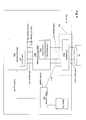
Fig. 1 is a schematic representation of portable electronic devices having ports connected through a bus to a computer in accordance with an embodiment; -
Fig. 2 is a block diagram of one device ofFig. 1 including its port; -
Fig. 3 is a block diagram of internal components of the device ofFig. 2 , including its port; -
Fig. 4 is a block diagram of internal components of the port ofFig. 3 ; and -
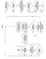
Fig. 5 is a flowchart of exemplary steps executed by an embodiment of in providing power to the device ofFig. 2 . - The description which follows and the embodiments described therein are provided by way of illustration of an example or examples of particular embodiments of the principles of the present disclosure. These examples are provided for the purposes of explanation and not limitation of those principles and of the invention. In the description which follows, like parts are marked throughout the specification and the drawings with the same respective reference numerals.
- The invention may provide a method for controlling interfacing parameters of a device when configured to be connectable to a host via a bus connection, comprising: establishing an initial connection by said device; charging a battery of said device using signals from said connection; conducting negotiations by said device to set a first data transmission rate for said device for said initial connection utilizing a communication bus controller contained in a microprocessor; said microprocessor operating in a low-power mode; and after detecting that the battery has been charged to a predetermined level, re-establishing said connection using a second bus controller in said device that processes said communications at a second transmission rate that is higher than said first data transmission rate.
- Preferably, when said connection is re-established, said microprocessor operates in a higher power mode than said low-power mode.
- Preferably, said bus is a Universal Serial Bus 'USB' bus; said first data transmission rate is a full-speed USB rate; and said second data transmission rate is a high-speed USB rate.
- Preferably, said second bus controller is external to said microprocessor.
- Preferably, said negotiations comprise: initiating a command to simulate an attachment; and generating and sending a signal by said device identifying that said device is capable of communicating at said first data transmission rate.
- Preferably, said negotiations further comprise initiating an enumeration process with a configuration that allows said device to terminate the enumeration process.
- Preferably, if said detecting completion of enumeration of said device is satisfied, said device: initiates a command to simulate a detachment; initiates a command to simulate an attachment; and identifies itself to said host as being capable of communicating at said second data transmission rate.
- Preferably, the method further comprising after said battery has been charged to said predetermined level, enumerating said connection from said second data transmission rate to said first data transmission rate.
- Preferably, said enumerating said connection comprises: initiating a command to simulate a detachment by said device from said host; initiating a command to simulate an attachment to said host; and generating and sending a signal identifying said device as being capable of communicating at said first data transmission rate.
- The invention may provide a controller for interfacing communications for a device, the controller configurable to be in operable connection to a host, the controller comprising: a first bus controller for processing said communications received at said device at a first data transmission rate; a second bus controller for processing said communications at a second transmission rate that is higher than said first data transmission rate; a controller module for activating said first bus controller while said device is establishing said connection and after completion of enumeration of said device, for activating said second bus controller; and a battery charging module for charging a battery powering said device, wherein while said device is establishing said connection, said battery charging module uses signals from said connection to charge said battery of said device and said microprocessor is arranged to operate in a low-power mode.
- Preferably, when said connection is re-established, said microprocessor is arranged to operate at a higher power mode than said low-power mode.
- Preferably, said bus comprises a Universal Serial Bus 'USB' bus; said first data transmission rate comprises a full-speed USB rate; and said second data transmission rate comprises a high-speed USB rate.
- Preferably, said controller module is arranged to initiate negotiations comprising: initiating a command to simulate an attachment; and generating a signal receivable by a host identifying that said device is capable of communicating at said first data transmission rate.
- Preferably, said negotiations further comprise initiating an enumeration process at said device by establishing a configuration for said device to allow said device to terminate the enumeration process.
- Preferably, if said detecting completion of enumeration of said device is satisfied, said controller module is arranged to: initiate a command to simulate a detachment; initiate a command to simulate an attachment; and generating a signal receivable by a host identifying that said device is being capable of communicating at said second data transmission rate.
- Preferably, said controller module is further arranged to initiate a second process to enumerate said connection from said second data transmission rate to said first data transmission rate, said second process being initiated upon satisfaction of a second predetermined condition.
- Preferably, said second process comprises: initiating a command to simulate a detachment by said device; initiating a command to simulate an attachment; and generating a signal receivable by a host identifying that said device is capable of communicating at said first data transmission rate.
- The invention may provide a computer readable medium storing computer readable instructions executable by a processor of a computing system to cause said system to implement the steps of the method.
- In a first aspect, a method for controlling interfacing parameters for a device when connected to a host may be provided. The method may comprise: monitoring for an initial connection by the device to the host; then, while the device is establishing the connection with the host, utilizing a communication bus controller contained in a microprocessor in the device to process communications with the host at a first data transmission rate; and after a predetermined condition, re-establishing the connection with the host using a second bus controller in the device that processes the communications at a second transmission rate that is higher than the first data transmission rate.
- In a second aspect, a method for controlling interfacing parameters for a device when connected to a host may be provided. The method may comprise: establishing an initial connection by the device to the host; conducting negotiations from the device to the host to set a first data transmission rate for the device for the initial connection utilizing a communication bus controller contained in a microprocessor; and after detecting a predetermined condition, re-establishing the connection with the host using a second bus controller in the device that processes the communications at a second transmission rate that is higher the first data transmission rate.
- In the method, while the device is establishing the connection: signals from the connection may be used to charge a battery of the device; and the microprocessor may operate in a low power mode.
- In the method, the predetermined condition may be the charging of the battery to a predetermined level.
- In the method, when the connection is re-established, the microprocessor may operate in a higher power mode than the low-power mode.
- In the method, the bus may be a USB bus, the first data transmission rate may be a full speed USB rate, the predetermined condition may be completion of enumeration of the device to the host, and the second data transmission rate may be a high speed USB rate.
- In the method, the second bus controller may be external to the microprocessor.
- In the method, the negotiations may comprise: initiating a command to simulate an attachment to the host; and identifying the device to the host as being capable of communicating at the first data transmission rate.
- In the method, the negotiations may further comprise initiating at the host an enumeration process with the device by establishing a configuration for the device to allow the device to terminate the enumeration process.
- In the method, if the predetermined condition is satisfied, the device may initiate a command to simulate a detachment from the host, may initiate a command to simulate an attachment to the host and may identify itself to the host as being capable of communicating at the second data transmission rate.
- The method may further comprise a second process to enumerate the connection from the second data transmission rate to the first data transmission rate, where the second process is initiated upon satisfaction of a second predetermined condition.
- In the method, the second process may comprise: initiating a command to simulate a detachment by the device from the host; initiating a command to simulate an attachment to the host; and identifying the device to the host as being capable of communicating at the first data transmission rate.
- In a third aspect, a system for interfacing communications for a device when connected to a host may be provided. The system may comprise: a first bus controller to process the communications between the device and the host at a first data transmission rate; a second bus controller to process the communications a second transmission rate that is higher the first data transmission rate; a module to monitor for an initial connection by the device to the host; and a controller module that activates the first bus controller while the device is establishing the connection with the host and after a predetermined condition, activates the second bus controller.
- The system may further comprise a battery charging module to charge a battery powering the device, wherein while the device is establishing the connection, signals from the connection may be used to charge the battery of the device and the microprocessor may operate in a low power mode.
- In the system, the predetermined condition may be the charging of the battery to a predetermined level and when the connection is re-established, the microprocessor may operate at a higher power mode than the low-power mode.
- In the system, the bus may be a USB bus, the first data transmission rate may be a full speed USB rate, the predetermined condition may be completion of enumeration of the device to the host and the second data transmission rate may be a high speed USB rate.
- In the system, the controller module may initiate negotiations comprising: initiating a command to simulate an attachment to the host; and identifying the device to the host as being capable of communicating at the first data transmission rate.
- In the system, the negotiations may further comprise initiating at the host an enumeration process with the device by establishing a configuration for the device to allow the device to terminate the enumeration process.
- In the system, if the predetermined condition is satisfied the controller module may initiate a command to simulate a detachment from the host, may initiate a command to simulate an attachment to the host and may identify the device to the host as being capable of communicating at the second data transmission rate.
- In the system, the controller module may further initiate a second process to enumerate the connection from the second data transmission rate to the first data transmission rate, where the second process may be initiated upon satisfaction of a second predetermined condition.
- In the system, the second process may comprise: initiating a command to simulate a detachment by the device from the host; initiating a command to simulate an attachment to the host; and identifying the device to the host as being capable of communicating at the first data transmission rate.
- In other aspects, various combinations of sets and subsets of the above aspects are provided.
- Generally, an embodiment provides a system and method for controlling a bus interface of a portable device that is connected to a host computer (or device) to allow for improved power management for the device.
- Exemplary details of embodiments are provided herein. First, a description is provided on general concepts and features of an embodiment and related bus management system(s). Then, further detail is provided on exemplary bus management systems related to an embodiment.
- Referring to
Fig. 1 , anenvironment 10 of an embodiment hashost computer 12 connected to a plurality of portableelectronic devices 14, such as cellphones, personal digital assistants (PDAs), portable gaming devices etc.Device 14A is a portable handheld device and connects to host 12 through itsport 18 viacable 20A.Devices device 12 through ahub 16.Hub 16 is connected to port 18 viacable 20B.Device 14B is connected to an output ofport 16 viacable 20C.Device 14C is connected tohub 16 viacable 20C, andhub 16 is connected to port 18 viacable 20D.Device 14B connects tohub 16 throughcradle 22 throughport 24 ondevice 14B. Whiledevices 14 are typically powered by internal batteries (not shown) the connections to host 12 allowhost 12 to provide a charging voltage todevices 14. In an embodiment,port 18 is a Universal Serial Bus (USB) port. - The USB specification defines electrical, mechanical and operational standards allowing devices to connect with a host through a standardized platform. Briefly, the USB bus is a bi-directional serial interface bus. Data is transmitted using a differential NRZI signals. Data may be transferred at one of three different rates from the host to the connected devices in speeds ranging from 10 Kbps to 480 Mbps: Slow speed mode (10 Kbps to 100 Kbps) is used for devices that have a low data transmission rate, such as a keyboard or a mouse; Full speed mode (500 Kbps to 10 Mbps) is used by more devices; and High speed mode (25 Mbps to 400 Mbps) is provided in USB version 2.0 and provides the highest data communication rate for the current standard. Notably, the High speed mode has certain electrical and mechanical requirements, including use of 45 ohm termination resisters between each data line and ground and minimum voltage and current levels for output signals generated for the High speed mode. It may be necessary to incorporate an additional bus transceiver to provide the required signal levels.
- As part of the USB specification, a USB port is allowed to supply power to devices that connect to it. As such, signals provided through
port 18 can be used to provide power todevice 14. A "high-power" USB port provides a voltage between 4.35-5.25 VDC and a current of at least 500 mA to its connected devices. A "low-power" USB port must be able to provide a voltage between 4.40-5.525 VDC and a current of 100 mA. - One feature of the USB specification allows devices to be connected (or "attached") and disconnected (or "detached") from the USB while either of the host or device is powered. The USB specification has a negotiation protocol that the host and device conduct to enable the host to determine when a new device attaches to the USB or when an attached device is detached from the USB. The USB provides an interrupt signal for reporting these events to the host. When a host is initially booted-up, it polls the root USB hub to determine whether any devices are attached. Thereafter, the host will periodically poll the hub(s) to determine whether any changes in the connected devices occurred.
- Generally, when a new device is connected to a host through a USB, the new device must be "enumerated". Per the USB specifications, enumeration determines what device has just been connected and the operating parameters of the device, such as power consumption, number and type of endpoint(s), class of product, etc. Enumeration is a process in which a connection is being established between a device and a host. When a device is being enumerated, the host send a series of requests to the device and the device is expected to reply. A typical enumeration process between a host operating under a Windows (trade-mark) platform and a device may generally be as follows:
- a) When a device is first plugged into connected to the USB port of the host, the host detects the device through a new voltage detected on the data lines of the USB. A USB connection circuit on the device provides the new voltage through a circuit providing through one or more pull-up resistor(s) connected to a voltage signal.
- b) After allowing time for the plug of the device to be fully inserted into the port and for power to stabilize on the device, the host may issue a reset command through the USB to reset the device to its default state.
- c) When the device receives the reset command, it is expected to reply with its address (such as address 0).
- d) The host then may attempt to retrieve device descriptor information from the device, through one or more requests.
- e) If a sufficient part of the device descriptor is received from the device, the host may issue a command to reset the bus. Thereafter the host may issue a command to set the address of the device. When the device receives the command it is expected to place itself in an "addressed state", per USB protocols.
- f) The host then may issue a request to the device for the remaining portion of the device descriptor.
- g) Thereafter the host may request configuration and string descriptor data from the device.
- One feature of the USB protocol is that a power signal can be provided by the host to its connected devices. As such, the current provided on the USB bus by the host can then be used to power components of the device. If the current in the signal is sufficiently large, the device may be fully activated when connected to the USB. The power may also charge an internal battery of the device.
- However, one operating parameter of the USB protocol imposes a current draw limitation on device when it is enumerating with the host. The present current limit is 100 mA. For some devices, they may need to draw more than 100 mA from the host to provide their full operation. Consider a device having a high speed USB controller operating at 480 Mbps and a transceiver generating any necessary USB-compliant signals for the device. When the device is operating in that mode, it may need more than 100 mA to power all of its modules and applications.
- Typically, at some point in the enumeration process, the device can indicate to the host via a message that it is "bus-powered" as opposed to "self-powered". Part of the message it can indicate that the device is requesting to draw 500mA. The host may deny the request, but must provide 100mA to the device at all times, per the USB standards.
- An embodiment provides a bus interface that allows a device to communicate with the host at one of several speeds through different bus modes, depending on the present state of connection of the device with the host and the present operating conditions of the device. Depending on the selected operating speed of the bus, the device may activate different modules, transceivers, internal components and may operate in different states. One mode is (lower) speed mode which bypasses additional hardware and software modules required for USB High speed communications. In the bypass mode, any High speed USB transceivers in the device may not need to be powered and USB bus control may be provided by an internal USB controller on the microprocessor of the device. Further the microprocessor may be able to operate in a lower-power mode. As such, when the device is operating in the bypass mode, it would use less power (and require less current from the USB) than when it would when operating in the High speed mode.
- The interface provides detection algorithms and circuits to determine: the operating state of the device, the USB connection state (e.g. whether the device is enumerating or not); and the current presently provided from the USB to the device. As such, while the bus interface is operating in the bypass mode, the interface can monitor for any (predetermined) necessary operating conditions that would allow the bus to operate at a higher speed. When those conditions are detected, the bus interface may change the operating state of the bus to a higher speed mode. In such a higher speed mode, additional circuitry may be activated and internal components of the device may be placed in a higher operating condition.
- Similarly, when the bus is operating in a high speed mode, the interface may monitor for any (predetermined) operating conditions that require that the bus operate at a lower speed and make any necessary changes to change the operating speed of the bus to a (suitable) lower speed and to disengage any components that are not needed for that lower speed. It will be appreciated that any number of speeds may be used. It will further be appreciated that other embodiments may be implemented that selectively activate and deactivate components that are related to features other than a bus for the device.
- Referring to
Fig. 1 , during execution of aspects of an embodiment whendevice 14 initially connects toUSB port 18 ofhost 12 and the device is enumerating with the host, a bus controller in device 14 (not shown) places the USB controller modules ofdevice 14 into a full speed bypass mode. In the bypass mode, the controller activates the internal USB port interface of the microprocessor ofdevice 14, disables the high speed USB transceiver ofdevice 14 and places the microprocessor into a low-power operating mode. During enumeration, signals received bydevice 14 fromhost 12 throughport 24 are provided directly to the microprocessor. As such, in the full speed bypass mode, all USB signals are handled by the internal USB port on the microprocessor and all data communication exchange rates are set to the limit set for the USB full speed mode. It will be seen that the controller utilizes less power to process signals betweenport 24 and the microprocessor and the high speed transceiver is not activated, thereby saving further power. It is noted that a typical USB baseband bus transceiver may draw between 10-15 mA of current in normal operation (in the full speed mode). A typical external high speed transceiver draws between 40mA and 50mA. As such, more current is conserved, which can be used to charge the battery ofdevice 14, until the USB controller ofdevice 14 can move to the high speed mode. - Once
device 14 enumerates withhost 12, the embodiment may provide a further status check on the power being provided from the USB. If the controller detects that the current is still being limited, (e.g. to 100 mA), then the controller may keep the bus operating in the full speed bypass mode and divert some of the current to charge the battery ofdevice 12. If the controller detects that there is more current available (e.g. if 500 mA is detected), then that additional current may alternatively be requested bydevice 14, while maintaining the data rate for the full speed mode. Once a predetermined condition is met (e.g. completion of sufficient charging of battery 342), the embodiment may allow the bus to switch to a higher operating speed. One method of changing the operating speed is to havedevice 14 re-enumerate to host 12. During the re-enumeration process, the new current availability values may be formally negotiating betweendevice 14 andhost 12. Once successful negotiations are complete, the microprocessor may be able to operate in its "normal" operating mode and more (or all) applications ondevice 14 may be activated. As part of the re-enumeration process, the bus may be set to operate in the USB High speed mode and expect to be able to draw 500 mA current from the USB. - In operation,
device 14 may initially set the bus interface to have its USB communications conducted using the full speed bypass mode to a maximum data rate as provided for full speed USB communications. Once the full speed bypass mode has been established and after the battery ondevice 14 is sufficiently charged,device 14 may initiate negotiations withhost 12 to go to the USB High speed mode. Once the High speed mode is set,device 14 may exchange data withhost 12 at the data rate provided for High speed USB communications. - An embodiment may additionally or alternatively have
device 14 operating the bus at a given speed and then automatically negotiate withhost 12 to determine whether the bus should be set at a lower speed. In such an embodiment,device 14 would need to request to disconnect from the USB then re-enumerate to re-establish a connection with the host. - Further detail is now provided on the basic operating components of
device 14, followed by a description of specific components more closely related to an embodiment. -
Fig. 2 provides general features ofelectronic device 14 for receiving electronic communications in accordance with an embodiment.Electronic device 14 is based on a computing platform having functionality of an enhanced personal digital assistant with cellphone and e-mail features. It is, however, to be understood thatelectronic device 14 can be based on construction design and functionality of other electronic devices, such as smart telephones, desktop computers, pagers or laptops having telephony equipment.Device 14 includes ahousing 200, anLCD 202,speaker 204, anLED indicator 206, atrackball 208, an ESC ("escape")key 210,keypad 212, a telephone headset comprised of anear bud 214 and amicrophone 216.Trackball 208 and ESC key 210 can be inwardly depressed along the path of arrow "A" as a means to provide additional input todevice 14.Port 24 provides a USB interface to eithercable 20D orcradle 22. - It will be understood that
housing 200 can be made from any suitable material as will occur to those of skill in the art and may be suitably formed to house and hold all components ofdevice 14. -
Device 14 is operable to conduct wireless telephone calls, using any known wireless phone system such as a Global System for Mobile Communications (GSM) system, Code Division Multiple Access (CDMA) system, Wideband CDMA/UMTS, CDMA 2000 system, Cellular Digital Packet Data (CDPD) system and Time Division Multiple Access (TDMA) system. Other wireless phone systems can include Bluetooth and the many forms of 802.11 wireless broadband, like 802.11a, 802.11b, 802.11g, etc. that support voice. Other embodiments include Voice over IP (VoIP) type streaming data communications that can simulate circuit-switched phone calls.Ear bud 214 can be used to listen to phone calls and other sound messages andmicrophone 216 can be used to speak into and input sound messages todevice 14. - Referring to
Fig. 3 , functional components ofdevice 14 are provided inschematic 300. The functional components are generally electronic, structural or electromechanical devices. In particular,microprocessor 302 is provided to control and receive almost all data, transmissions, inputs and outputs related todevice 14.Microprocessor 302 is shown schematically as coupled tokeypad 212,port 24 and other internal devices.Microprocessor 302 preferably controls the overall operation of thedevice 14 and its components. Exemplary microprocessors formicroprocessor 302 include Data 950 (trade-mark) series microprocessors, the 6200 series microprocessors and the PXA900 series of microprocessors, all available at one time from Intel Corporation.Microprocessor 302 is connected to other elements indevice 14 through a series of electrical connections to its various input and output pins.Microprocessor 302 has an IRQ input line which allows it to receive signals from various devices. Appropriate interrupt firmware is provided which receives and reacts to the signals detected on the IRQ line.Microprocessor 302 may operate in several power modes, including a "normal" mode and a low-power mode. Also,microprocessor 302 may have one or more built-in modules such as a digital to analog converter, an analog to digital converter and aUSB bus controller 352. - In addition to the
microprocessor 302, other internal components of thedevice 14 are shown schematically inFig. 3 . These include:display 202;speaker 204;keypad 212;communication sub-system 304; short-range communication sub-system 306; auxiliary I/O devices 308;port 24;microphone port 310 formicrophone 216; flash memory 312 (which provides persistent storage of data); random access memory (RAM) 314;clock 316 and other device sub-systems (not shown).Device 14 is preferably a two-way radio frequency (RF) communication device having voice and data communication capabilities. In addition,device 14 preferably has the capability to communicate with other computer systems via the Internet. -
Port 24 provides a physical connection interface tocable 20D and / orcradle 22.Port 24 also comprises an interface circuit to selectively connect and disconnect and control signals that pass betweenmicroprocessor 302 and the connection interface. Further detail onport 24 is provided below. - Operating system software executed by the
microprocessor 302 is preferably stored in a computer-readable medium, such asflash memory 312, but may be stored in other types of memory devices, such as read-only memory (ROM) or similar storage element. In addition, system software, specific device applications, or parts thereof, may be temporarily loaded into a volatile store, such asRAM 314. Communication signals received bydevice 14 may also be stored toRAM 314. -
Microprocessor 302, in addition to its operating system functions, enables execution of software applications ondevice 14. A set of software (or firmware) applications, generally identified as applications 318, that control basic device operations, such asvoice communication module 318A anddata communication module 318B, may be installed on thedevice 14 during manufacture or downloaded thereafter. As well, software modules, such ascalendar module 318C,address book 318D andlocation module 318E. Additional modules such as personal information manager (PIM) application may be provided. Any module may be installed during manufacture or downloaded thereafter intodevice 14. Data associated with each application can be stored inflash memory 312. Also,Port Control Code 318N is provided to control operation ofdevice 14 and its internal bus connections withport 24 whendevice 14 is connected to host 12. Further detail onPort Control Code 318N is provided below. - Communication functions, including data and voice communications, are performed through the
communication sub-system 304 and the short-range communication sub-system 306.Systems device 14. For example, ifdevice 14 is in a low-power mode, then either or both ofsystems systems sub-systems device 14. Various applications 318 provide the operational controls to further process and log the communications.Communication sub-system 304 includesreceiver 320,transmitter 322 and one or more antennas, illustrated as receiveantenna 324 and transmitantenna 326. In addition,communication sub-system 304 also includes processing modules, such as digital signal processor (DSP) 328 and local oscillators (LOs) 340. The specific design and implementation ofcommunication sub-system 304 is dependent upon the communication network in whichdevice 14 is intended to operate. For example,communication sub-system 304 ofdevice 14 may operate with the Mobitex (trade-mark), DataTAC (trade-mark) or General Packet Radio Service (GPRS) mobile data communication networks and also operate with any of a variety of voice communication networks, such as Advanced Mobile Phone Service (AMPS), Time Division Multiple Access (TDMA), Code Division Multiple Access (CDMA), CDMA 2000, Personal Communication Service (PCS), Global System for Mobile Communication (GSM), etc. Other types of data and voice (telephonic) networks, both separate and integrated, may also be utilized withdevice 14. In any event,communication sub-system 304 providesdevice 14 with the capability of communicating with other devices using various communication technologies, including instant messaging (IM) systems, text messaging (TM) systems and short message service (SMS) systems. - In addition to processing communication signals,
DSP 328 provides control ofreceiver 320 andtransmitter 322. For example, gains applied to communication signals inreceiver 320 andtransmitter 322 may be adaptively controlled through automatic gain-control algorithms implemented inDSP 328. - In a data communication mode, a received signal, such as a text message or Web page download, is processed by the
communication sub-system 304 and is provided as an input tomicroprocessor 302. The received signal is then further processed bymicroprocessor 302 which can then generate an output to display 202 or to an auxiliary I/O device 308. A device user may also compose data items, such as e-mail messages, usingkeypad 212,trackball 208 and/or some other auxiliary I/O device 308, such as a touchpad, a rocker switch, a trackball or some other input device. The composed data items may then be transmitted over a communication network viacommunication sub-system 304.Sub-system 304 may also detect when it is out of communication range for its remote systems. - In a voice communication mode, overall operation of
device 14 is substantially similar to the data communication mode, except that received signals are output tospeaker 204, and signals for transmission are generated bymicrophone 216. Alternative voice or audio I/O sub-systems, such as a voice message recording sub-system, may also be implemented ondevice 14. In addition,display 202 may also be utilized in voice communication mode, for example, to display the identity of a calling party, the duration of a voice call, or other voice call-related information. - Short-
range communication sub-system 306 enables communication betweendevice 14 and other proximate systems or devices, which need not necessarily be similar devices. For example, the short-range communication sub-system may include an infrared device and associated circuits and components, or a Bluetooth (trade-mark) communication module to provide for communication with similarly enabled systems and devices. -
Device 14 may also haveglobal positioning system 344 to assist in identifying a present location ofdevice 14 and may also havelight sensor 346 to provide data on the ambient light conditions fordevice 14. These elements may be controlled by software operating ondevice 14 as described earlier. - Powering the entire electronics of the mobile handheld communication device is
power source 342. In one embodiment, thepower source 342 includes one or more batteries. In another embodiment, thepower source 342 is a single battery pack, especially a rechargeable battery pack. A power switch (not shown) provides an "on/off" switch fordevice 14.Battery charging circuit 348 provides a hardware interface to allow external power to be selectively provided todevice 14. Such power may be provided through signals received inport 24. The charging circuit may be able to detect the present level of charge onbattery 342 and determine whetherbattery 342 is sufficiently charged. A sufficient level of charge can differ among devices and batteries. Determining a level of charge may be implemented using circuits and techniques known in the art. A power source interface (not shown) may be provided in hardware, firmware, software or a combination of such elements to selectively control access of components indevice 14 topower source 342. Upon activation of the power switch an application 318 is initiated to turn ondevice 14. Upon deactivation of the power switch, an application 318 is initiated to turn offdevice 14. Power todevice 14 may also be controlled by other devices and by software applications 318. -
Port 24 provides signals fromconnector 20 tomicroprocessor 302 throughport controller 352. As is described further below,controller 352 selectively engages a bus transceiver whendevice 14 is operating in a high speed mode for USB signals. Controller also communicates with internal USB port 350 inmicroprocessor 302. USB port 350 can selectively communicate directly withport 24, as controlled bycontroller 352. - Further detail is now provided on specific components of
device 14 as they relate to an embodiment. First, detail is provided on the bus interface and the controller fordevice 14 forport 24 andPort Control Code 318N. -
Fig. 4 shows diagram 400 of components ofdevice 14 includingport 24 and internal components that process signals carried thereon.Connector 402 is part ofport 24 and provides a physical connector forcable 20 todevice 14. USB signals 410 are provided betweenconnector 402 andmicroprocessor 302.Controller 352 provides control logic to selectively make signalling connections betweenmicroprocessor 302 andport 24 for USB signals 410.Microprocessor 302 is controlled, in part byPort Control Code 318N. Data and control signals received bymicroprocessor 302 through USB signals 410 allow an embodiment to determine the present state of connection ofdevice 14 to host 12. As such, an embodiment can then causemicroprocessor 302 to selectively generate: control signals 408 to control one or more of controller 352 (and its elements); host interface signals 412 and USB signals 410 to communicate withhost 14. It will be appreciated that there is a separate data path between the host andcontroller 352 aside from the USB connection. The USB path allows the (full speed) USB port 350 to be "routed through" (high speed)port controller 352. In such a "routed through" state, it will be typical that much of the circuitry incontroller 352 would not be powered. USB signals 410 frommicroprocessor 302 are processed either by USB port 350 alone or by port 350 withtransceiver 404, depending on the state of operation of the USB fordevice 14. Power and control is also provided to chargingcircuit 348, which selectively provides either the 100mA signal or the 500 mA signal to a charging circuit that chargesbattery 342. The battery may be charged to any sufficient predetermined level bycircuit 348 depending on its design.Circuit 348 receives a Vbus signal fromconnector 402 and control signals fromcontroller 352 andmicroprocessor 302. - Within
controller 352,transceiver circuit 404 is provided to selectively amplify signals frommicroprocessor 302 destined toport 24.Transceiver 404 may include USB bus logic to allow it to generate USB compliant signals based on signals 408 received frommicroprocessor 302. Current detectcircuit 406 provides electroniccircuits allowing controller 352 to determine the level of current and/or voltage present in USB signals 410. The controller may have a digital memory (endpoint RAM) interface for the host, a phase-locked loop to generate a clock forcontroller 352 and encoders and decoders for NRZI signalling conversion, in addition to USB bypass routing logic. The controller has logic to selectively charge battery through chargingcircuit 348 at either 100 mA or 500 mA based on a charging message received by the device from the host indicating what is available. - Further detail is now provided on
Port Control Code 318N as it controls elements ofdevice 14. - Referring to
Fig. 5 ,flow chart 500 shows an exemplary process used to control operation of the USB bus andcontroller 352 fordevice 14 throughPort Control Code 318N. Overall,code 318N operates ondevice 14 and controlsport controller 352, internal USB port 350 and chargingcircuit 348. - At
block 502,Port Control Code 318N starts. Initiation ofCode 318N may be automatically executed on startup ofdevice 14 or upon detection of a connection being established through port 24 (Fig. 4 ). Atstep 504, the process waits for detection of a connection to host 12. - Next, at
test block 506, the signals on USB signals 410 are monitored to determine whether if a connection has been detected. If no connection has been detected, then the process returns to step 504. If a connection has been detected, the process moves to step 508, where a transmission mode for the bus is determined, based on USB signals 410 as processed byCode 318N. For example, the connection maybe: a high-speed, a full-speed, a low-speed connection, high-impedance or a different connection. The type of connection may be determined from signals received fromhost 12 or by evaluating the physical characteristics of the signals (e.g. the current, using current detect module 406). As such, attest 510, the process evaluates whether the connection is a high speed connection. If it is, the process moves to step 512 where the controller is set to a full speed bypass mode. In other embodiments, the default may be to simply forcedevice 14 into the bypass mode. Iftest 510 is conducted and if it determines that the present USB connection is not a high speed connection, then the process moves directly fromtest 510 to step 514. - After the bypass mode is set, the process moves to step 514 where an enumeration process is started with the host. During enumeration,
Code 318N may generate messages destined forhost 12 throughport 24 thatdevice 14 is operating in a full speed mode (i.e. the bypass mode). - Optionally, if any current is available through USB signals 410 for charging
battery 342 through chargingcircuit 348, then the battery is charged.Code 318N may selectively activate current detectmodule 406 to determine the level of current of USB signals 410 and then selectively activate charging circuit 348 (Fig. 3 ) to chargebattery 342. Alternatively or additionally, such information may be derived from the contents of USB signals 410 fromhost 12.Circuit 348 may provide a "charge" signal which is detected bymicroprocessor 302 and assuch Code 318N. Upon detection of any "charge" signal, the charging process may be stopped. - Next, at
test 516, the process detects whether the enumeration is complete. If it is not complete then the test return to step 514 to complete the enumeration. If the enumeration is complete, the process moves to step 518, where the current provided on the bus is detected usingCode 318N to evaluate data provided by eithercurrent detector circuit 406 or messages provided fromhost 14. In some instances, host-side drivers may inform the device of what the available current is on the port that the device is connected to. This may be done through a setup message sent during enumeration. As such in some instances, thestep 518 may be conducted elsewhere in the process. - Thereafter, the process moves to step 520 where the charge on the battery is determined. This charge may be evaluated by charging
circuit 348. This step is optional and it may be conducted as part ofstep 514. - Then the process moves to step 526 where a test is made to determine whether there is a sufficient charge on
battery 342. If the battery is not charged then the process returns to step 524 to maintain the bus in full speed bypass mode. However, if the battery is charged, then theprocess 500 moves to step 528, where the bus is re-enumerated to a high speed mode. At this point, the following test can also be done: if the re-enumeration is not successful (e.g. the host rejects the connect at the high speed mode and instead offers the full speed mode), then the system returns to the bypass mode. Thereafter if re-enumeration is complete and successful, the bus is activated at the high speed level. This may include activatingtransceiver 504. The next step is the end of the process. - Alternatively, once an embodiment sets the full speed bypass mode for
device 14, if either 100 mA or 500 mA is available fromhost 12,device 14 may issue a USB command to accepts signals being transmitted at either current level. However, the data rate would remain limited to the ranges provided by the Full speed USB standard. - It will be appreciated that this process may be initiated upon the detection of a connection, as provided in
step 504. However, in other embodiments other external conditions may trigger the activation of theprocess 500. For example, the process may be restarted if the current is detected to drop to 100 mA, i.e. the bus drops down to a full speed mode. It will be appreciated that thisprocess 500 utilizes signals frommicroprocessor 302 andPort Control Code 318N. - In another embodiment, an algorithm may be implemented in
Port Control Code 318N to control management of a captive USB bus from a full speed mode to a high speed mode as follows. First,device 14 boots up with a USB cable connected to host 12.Next device 14 simulates an "attachment" to host 12 through a USB signal anddevice 14 identifies itself to host 12 as a full-speed capable (but not high speed capable) device. - Once
host 12 receives and interprets this identification,host 12 initiates an USB enumeration process withdevice 14. As part of the enumeration process, host 12 sets the USB configuration fordevice 14 to allowdevice 14 to terminate the enumeration process. - Next, a test is made at
device 14 to determine whetherdevice 14 has sufficient power to operate in the USB high speed mode. If it does not, thendevice 14 may initiate any appropriate action to meet the power requirements, reset and then return to the boot up step. Ifdevice 14 has sufficient power, then through signal(s) provided by the device on the USB, device 14: simulates a detach from the USB; simulates an attach; and identifies itself to host 12 as being high speed capable. At that time,host 12 initiates an enumeration process and sets the USB configuration fordevice 14 to allowdevice 14 to terminate the enumeration process. At that time,device 14 is enumerated at the high speed mode. As noted earlier, all steps are executed through command and control signals generated byPort Control Code 318N and provided to USB and other elements indevice 14. - As a complementary process,
Port Control Code 318N has a separate process to manage and control negotiation of its USB from being enumerated at a high speed mode to a full speed mode. For this process,device 14 starts as being enumerated at the high speed mode. Next, a test is periodically conducted to determine ifdevice 14 needs to down grade to the full speed mode. Different conditions may be set that require the downgrade. Conditions may include: current power state, current time, current location or other criteria. If the results of the test indicates thatdevice 14 should remain at high speed mode, it continues to operate at that mode. However, if the results indicate that a downgrade should be performed, thendevice 14 simulates a detach and then an attach to the USB. Next,device 14 identifies itself to host 12 as being full-speed capable (but not high speed capable). Oncehost 12 receives and interprets this identification,host 12 initiates an USB enumeration process withdevice 14. As part of the enumeration process, host 12 sets the USB configuration fordevice 14 to allowdevice 14 to terminate the enumeration process and finallydevice 14 is enumerated a full speed. - It will be appreciated that the
Port Control Code 318N and other applications in the embodiments can be implemented using known programming techniques, languages and algorithms. The titles of the modules are provided as a convenience to provide labels and assign functions to certain modules. It is not required that each module perform only its functions as described above. As such, specific functionalities for each application may be moved between applications or separated into different applications. Different signalling techniques may be used to communicate information between applications using known programming techniques. Known data storage, access and update algorithms allow data to be shared between applications. For example, detection or completion of an event described inFig. 5 or any process executing ondevice 14 may cause an interrupt to be generated onmicroprocessor 302 and a particular interrupt routine may be provided to process the event. It will further be appreciated that other applications and systems ondevice 14 may be executing concurrently withCode 318N. As such,Code 318N may be structured to operate in as a "background" application ondevice 14, using programming techniques known in the art. - While an embodiment has been described where a bus is selectively operated in different modes while
device 14 is enumerating withhost 12, it will be appreciated that other comparable embodiments may be implemented to operate independently from whether or notdevice 14 is enumerating. Also an embodiment may be directed to a USB protocol or a different bus architecture. Further, other embodiments may provide selective activation and deactivation of other components to conserve power, depending on the present operating environment ofdevice 14. For example, during a powering cycle,communication subsystems - It will be appreciated that other embodiments may incorporate wireless connections and charging systems.
- The present invention is defined by the claims appended hereto, with the foregoing description being merely illustrative of embodiments of the invention. Those of ordinary skill may envisage certain modifications to the foregoing embodiments which, although not explicitly discussed herein, do not depart from the scope of the invention, as defined by the appended claims.
Claims (15)
- A method for controlling interfacing parameters on a device configured to be connectable to a host via a bus connection, comprising:establishing an initial connection by said device;charging a battery of said device using signals from said connection;conducting negotiations by said device to set a first data transmission rate for said device for said initial connection utilizing a communication bus controller contained in a microprocessor;said microprocessor operating in a low-power mode; andafter detecting that the battery has been charged to a predetermined level, re-establishing said connection using a second bus controller in said device that processes said communications at a second transmission rate that is higher than said first data transmission rate.
- The method as claimed in claim 1, wherein when said connection is re-established, said microprocessor operates in a higher power mode than said low-power mode.
- The method as claimed in any one claims 1 or 2, wherein:said bus is a Universal Serial Bus 'USB' bus;said first data transmission rate is a full speed USB rate;said second data transmission rate is a high speed USB rate.
- The method as claimed in any one of the preceding claims, wherein said negotiations comprise:initiating a command to simulate an attachment;generating and sending a signal by said device identifying that said device is capable of communicating at said first data transmission rate; andpreferably initiating an enumeration process with a configuration that allows said device to terminate the enumeration process.
- The method as claimed in claim 4, wherein if said detecting completion of enumeration of said device is satisfied, said device:initiates a command to simulate a detachment;initiates a command to simulate an attachment; andidentifies itself to said host as being capable of communicating at said second data transmission rate.
- The method claimed in claim 5, further comprising after said battery has been charged to said predetermined level, enumerating said connection from said second data transmission rate to said first data transmission rate.
- The method as claimed in claim 6, wherein said enumerating said connection comprises:initiating a command to simulate a detachment by said device from said host;initiating a command to simulate an attachment to said host; andgenerating and sending a signal identifying said device as being capable of communicating at said first data transmission rate.
- A controller for interfacing communications for a device, the controller configurable to be in operable connection to a host, the controller comprising:a first bus controller for processing said communications received at said device at a first data transmission rate;a second bus controller for processing said communications at a second transmission rate that is higher than said first data transmission rate;a controller module for activating said first bus controller while said device is establishing said connection and after completion of enumeration of said device, for activating said second bus controller; anda battery charging module for charging a battery powering said device,wherein while said device is establishing said connection, said battery charging module uses signals from said connection to charge said battery of said device and said microprocessor is arranged to operate in a low power mode.
- The controller as claimed in claim 8, wherein when said connection is re-established, said microprocessor is arranged to operate at a higher power mode than said low-power mode.
- The controller as claimed in any one of claims 9 or 10, wherein:said bus comprises a Universal Serial Bus 'USB' bus;said first data transmission rate comprises a full speed USB rate; andsaid second data transmission rate comprises a high speed USB rate.
- The controller as claimed in any one of claims 9 to 11, wherein:said controller module is arranged to initiate negotiations comprising:initiating a command to simulate an attachment; andgenerating a signal receivable by a host that said device is capable of communicating at said first data transmission rate;andpreferably said negotiations further comprise initiating an enumeration process at said device by establishing a configuration for said device to allow said device to terminate the enumeration process.
- The controller as claimed in claim 11, wherein if said detecting completion of enumeration of said device is satisfied, said controller module is arranged to:initiate a command to simulate a detachment;initiate a command to simulate an attachment; andgenerate a signal receivable by a host that said device is capable of communicating at said second data transmission rate.
- The controller as claimed in claim 12, wherein said controller module is further arranged to initiate a second process to enumerate said connection from said second data transmission rate to said first data transmission rate, said second process being initiated upon satisfaction of a second predetermined condition.
- The controller as claimed in claim 13, wherein said second process comprises: initiating a command to simulate a detachment by said device;initiating a command to simulate an attachment; andgenerating a signal receivable by a host identifying that said device is capable of communicating at said first data transmission rate.
- A computer readable medium storing computer readable instructions executable by a processor of a computing system to cause said system to implement the steps of the method of any one of claims 1 to 7.
Applications Claiming Priority (1)
| Application Number | Priority Date | Filing Date | Title |
|---|---|---|---|
| EP07108895A EP1995666B1 (en) | 2007-05-24 | 2007-05-24 | System and method for interfacing an electronic device with a host system |
Related Parent Applications (2)
| Application Number | Title | Priority Date | Filing Date |
|---|---|---|---|
| EP07108895.9 Division | 2007-05-24 | ||
| EP07108895A Division EP1995666B1 (en) | 2007-05-24 | 2007-05-24 | System and method for interfacing an electronic device with a host system |
Publications (2)
| Publication Number | Publication Date |
|---|---|
| EP2107469A1 true EP2107469A1 (en) | 2009-10-07 |
| EP2107469B1 EP2107469B1 (en) | 2013-04-03 |
Family
ID=38710060
Family Applications (3)
| Application Number | Title | Priority Date | Filing Date |
|---|---|---|---|
| EP09163768A Not-in-force EP2107469B1 (en) | 2007-05-24 | 2007-05-24 | System and method for interfacing an electronic device with a host system |
| EP07108895A Active EP1995666B1 (en) | 2007-05-24 | 2007-05-24 | System and method for interfacing an electronic device with a host system |
| EP09163756A Not-in-force EP2107468B1 (en) | 2007-05-24 | 2007-05-24 | System and method for interfacing an electronic device with a host system |
Family Applications After (2)
| Application Number | Title | Priority Date | Filing Date |
|---|---|---|---|
| EP07108895A Active EP1995666B1 (en) | 2007-05-24 | 2007-05-24 | System and method for interfacing an electronic device with a host system |
| EP09163756A Not-in-force EP2107468B1 (en) | 2007-05-24 | 2007-05-24 | System and method for interfacing an electronic device with a host system |
Country Status (6)
| Country | Link |
|---|---|
| EP (3) | EP2107469B1 (en) |
| CN (1) | CN101441612B (en) |
| AT (1) | ATE528716T1 (en) |
| CA (1) | CA2631955C (en) |
| DE (1) | DE602007001594D1 (en) |
| ES (1) | ES2329091T3 (en) |
Families Citing this family (10)
| Publication number | Priority date | Publication date | Assignee | Title |
|---|---|---|---|---|
| CN101520767B (en) * | 2009-04-07 | 2011-02-09 | 上海炬力集成电路设计有限公司 | Data transmission speed self-adapting method and device |
| CN101998691B (en) * | 2009-08-26 | 2013-10-16 | 中兴通讯股份有限公司 | Method, system and device for data transmission |
| TWI450531B (en) * | 2011-08-22 | 2014-08-21 | Edgecore Networks Corp | Network device and port function setting method thereof |
| KR101844287B1 (en) | 2012-02-03 | 2018-04-02 | 삼성전자 주식회사 | Method and apparatus for charging battery |
| KR20130122266A (en) * | 2012-04-30 | 2013-11-07 | 삼성전자주식회사 | System and apparatus and method for performing charging in host mode |
| CN103677197B (en) * | 2012-08-30 | 2017-08-25 | 中兴通讯股份有限公司 | The electricity saving method and device of USB data transmission system |
| CN105760327B (en) * | 2015-12-10 | 2019-09-17 | 中国电子科技集团公司第三十二研究所 | Internal bus of aerospace electronic product |
| CN109426644A (en) * | 2017-08-31 | 2019-03-05 | 西安中兴新软件有限责任公司 | A kind of rate adjusting method and device, equipment of USB data transmission |
| NL2025755B1 (en) * | 2020-06-04 | 2022-01-26 | Microsoft Technology Licensing Llc | Systems and methods of controlling communication modes in an electronic device |
| CN115313597B (en) * | 2022-08-26 | 2025-12-05 | 歌尔科技有限公司 | A dual-battery power supply system and electronic device |
Citations (2)
| Publication number | Priority date | Publication date | Assignee | Title |
|---|---|---|---|---|
| US20050066087A1 (en) * | 1999-12-24 | 2005-03-24 | Wu Zong Liang | Emulation of a disconnect of a device |
| EP1775652A1 (en) * | 2005-10-13 | 2007-04-18 | Research In Motion Limited | Apparatus and method to support USB enumeration of a BUS powered handheld device |
Family Cites Families (4)
| Publication number | Priority date | Publication date | Assignee | Title |
|---|---|---|---|---|
| US5974486A (en) * | 1997-08-12 | 1999-10-26 | Atmel Corporation | Universal serial bus device controller comprising a FIFO associated with a plurality of endpoints and a memory for storing an identifier of a current endpoint |
| US6279060B1 (en) * | 1998-12-04 | 2001-08-21 | In-System Design, Inc. | Universal serial bus peripheral bridge simulates a device disconnect condition to a host when the device is in a not-ready condition to avoid wasting bus resources |
| EP1516261B1 (en) * | 2002-06-12 | 2008-08-06 | Nxp B.V. | Bus system, station for use in a bus system, and bus interface |
| US7685328B2 (en) * | 2004-09-09 | 2010-03-23 | Stmicroelectronics, Inc. | Generic universal serial bus device operable at low and full speed and adapted for use in a smart card device |
-
2007
- 2007-05-24 ES ES07108895T patent/ES2329091T3/en active Active
- 2007-05-24 AT AT09163756T patent/ATE528716T1/en not_active IP Right Cessation
- 2007-05-24 EP EP09163768A patent/EP2107469B1/en not_active Not-in-force
- 2007-05-24 EP EP07108895A patent/EP1995666B1/en active Active
- 2007-05-24 DE DE602007001594T patent/DE602007001594D1/en active Active
- 2007-05-24 EP EP09163756A patent/EP2107468B1/en not_active Not-in-force
-
2008
- 2008-05-21 CA CA2631955A patent/CA2631955C/en active Active
- 2008-05-23 CN CN2008101842567A patent/CN101441612B/en not_active Expired - Fee Related
Patent Citations (2)
| Publication number | Priority date | Publication date | Assignee | Title |
|---|---|---|---|---|
| US20050066087A1 (en) * | 1999-12-24 | 2005-03-24 | Wu Zong Liang | Emulation of a disconnect of a device |
| EP1775652A1 (en) * | 2005-10-13 | 2007-04-18 | Research In Motion Limited | Apparatus and method to support USB enumeration of a BUS powered handheld device |
Non-Patent Citations (1)
| Title |
|---|
| "Universal Serial Bus Specification Revision 2.0", 27 April 2000, USB IMPLEMENTERS FORUM, XP002460358 * |
Also Published As
| Publication number | Publication date |
|---|---|
| CN101441612A (en) | 2009-05-27 |
| ATE528716T1 (en) | 2011-10-15 |
| EP1995666A1 (en) | 2008-11-26 |
| EP2107468B1 (en) | 2011-10-12 |
| CN101441612B (en) | 2010-12-08 |
| CA2631955A1 (en) | 2008-11-24 |
| EP2107469B1 (en) | 2013-04-03 |
| EP2107468A1 (en) | 2009-10-07 |
| DE602007001594D1 (en) | 2009-08-27 |
| EP1995666B1 (en) | 2009-07-15 |
| ES2329091T3 (en) | 2009-11-20 |
| CA2631955C (en) | 2012-09-18 |
Similar Documents
| Publication | Publication Date | Title |
|---|---|---|
| US7631126B2 (en) | System and method for interfacing an electronic device with a host system | |
| EP2107468B1 (en) | System and method for interfacing an electronic device with a host system | |
| EP3404541B1 (en) | Application control method and related device | |
| US20130254571A1 (en) | Power management method and apparatus for network access module | |
| EP3671451B1 (en) | Method of automatically releasing resource occupied by background process of terminal, storage medium and terminal | |
| CN110520854B (en) | Electronic device with USB Type C interface, control method and readable storage medium | |
| US11947481B2 (en) | Terminal and type C interface anti-corrosion method | |
| KR20160147706A (en) | System and method for disconnect detection on a dual mode port of a usb hub | |
| EP3496505A1 (en) | Data migration method and related devices | |
| KR20090084488A (en) | Method and apparatus for determining external device connected to mobile terminal | |
| CN106095566B (en) | Response control method and mobile terminal | |
| CA2562776C (en) | Apparatus and method to support usb enumeration of a bus powered handheld device | |
| CN110620602B (en) | Reverse charging and data transmission sharing system, multiplexing data lines and electronic devices | |
| WO2021063274A1 (en) | Charging control method and apparatus therefor, electronic device and computer storage medium | |
| CN108777627B (en) | A power supply method and device | |
| CN108475097B (en) | A power management method and terminal equipment | |
| EP3407192A1 (en) | Method for assigning installation task and mobile terminal | |
| CN113722260A (en) | Protection circuit, serial bus system, circuit protection method and mobile terminal | |
| CN105098854A (en) | Charging method and electronic device | |
| CN112256610B (en) | Connection control method, system, storage medium and mobile terminal | |
| EP2381368A1 (en) | Motherboard with rapid battery charging option on a connection port | |
| CN112261634A (en) | Bluetooth transmission control method, device, terminal equipment and storage medium | |
| CN111371154B (en) | Charging structure, charging method and terminal | |
| CN119651814A (en) | Method, device, equipment and storage medium for switching fast charging protocol of charging device | |
| CN112491562A (en) | Communication control method and device and mobile terminal |
Legal Events
| Date | Code | Title | Description |
|---|---|---|---|
| PUAI | Public reference made under article 153(3) epc to a published international application that has entered the european phase |
Free format text: ORIGINAL CODE: 0009012 |
|
| 17P | Request for examination filed |
Effective date: 20090625 |
|
| AC | Divisional application: reference to earlier application |
Ref document number: 1995666 Country of ref document: EP Kind code of ref document: P |
|
| AK | Designated contracting states |
Kind code of ref document: A1 Designated state(s): AT BE BG CH CY CZ DE DK EE ES FI FR GB GR HU IE IS IT LI LT LU LV MC MT NL PL PT RO SE SI SK TR |
|
| 17Q | First examination report despatched |
Effective date: 20091111 |
|
| GRAP | Despatch of communication of intention to grant a patent |
Free format text: ORIGINAL CODE: EPIDOSNIGR1 |
|
| RIN1 | Information on inventor provided before grant (corrected) |
Inventor name: WINGER, LYALL Inventor name: MATTON, MAXIME Inventor name: WOOD, ROBERT Inventor name: GOLDSMITH, MICHAEL Inventor name: MAILLOUX, JERRY Inventor name: BARAKE, OMAR |
|
| GRAP | Despatch of communication of intention to grant a patent |
Free format text: ORIGINAL CODE: EPIDOSNIGR1 |
|
| GRAS | Grant fee paid |
Free format text: ORIGINAL CODE: EPIDOSNIGR3 |
|
| GRAA | (expected) grant |
Free format text: ORIGINAL CODE: 0009210 |
|
| AC | Divisional application: reference to earlier application |
Ref document number: 1995666 Country of ref document: EP Kind code of ref document: P |
|
| AK | Designated contracting states |
Kind code of ref document: B1 Designated state(s): AT BE BG CH CY CZ DE DK EE ES FI FR GB GR HU IE IS IT LI LT LU LV MC MT NL PL PT RO SE SI SK TR |
|
| REG | Reference to a national code |
Ref country code: GB Ref legal event code: FG4D |
|
| REG | Reference to a national code |
Ref country code: CH Ref legal event code: EP Ref country code: AT Ref legal event code: REF Ref document number: 605107 Country of ref document: AT Kind code of ref document: T Effective date: 20130415 |
|
| REG | Reference to a national code |
Ref country code: IE Ref legal event code: FG4D |
|
| REG | Reference to a national code |
Ref country code: DE Ref legal event code: R096 Ref document number: 602007029521 Country of ref document: DE Effective date: 20130529 |
|
| REG | Reference to a national code |
Ref country code: CH Ref legal event code: PFA Owner name: BLACKBERRY LIMITED, CA Free format text: FORMER OWNER: RESEARCH IN MOTION LIMITED, CA Ref country code: AT Ref legal event code: MK05 Ref document number: 605107 Country of ref document: AT Kind code of ref document: T Effective date: 20130403 |
|
| PG25 | Lapsed in a contracting state [announced via postgrant information from national office to epo] |
Ref country code: SI Free format text: LAPSE BECAUSE OF FAILURE TO SUBMIT A TRANSLATION OF THE DESCRIPTION OR TO PAY THE FEE WITHIN THE PRESCRIBED TIME-LIMIT Effective date: 20130403 |
|
| RAP2 | Party data changed (patent owner data changed or rights of a patent transferred) |
Owner name: BLACKBERRY LIMITED |
|
| REG | Reference to a national code |
Ref country code: NL Ref legal event code: T3 |
|
| REG | Reference to a national code |
Ref country code: LT Ref legal event code: MG4D |
|
| PG25 | Lapsed in a contracting state [announced via postgrant information from national office to epo] |
Ref country code: FI Free format text: LAPSE BECAUSE OF FAILURE TO SUBMIT A TRANSLATION OF THE DESCRIPTION OR TO PAY THE FEE WITHIN THE PRESCRIBED TIME-LIMIT Effective date: 20130403 Ref country code: AT Free format text: LAPSE BECAUSE OF FAILURE TO SUBMIT A TRANSLATION OF THE DESCRIPTION OR TO PAY THE FEE WITHIN THE PRESCRIBED TIME-LIMIT Effective date: 20130403 Ref country code: IS Free format text: LAPSE BECAUSE OF FAILURE TO SUBMIT A TRANSLATION OF THE DESCRIPTION OR TO PAY THE FEE WITHIN THE PRESCRIBED TIME-LIMIT Effective date: 20130803 Ref country code: BE Free format text: LAPSE BECAUSE OF FAILURE TO SUBMIT A TRANSLATION OF THE DESCRIPTION OR TO PAY THE FEE WITHIN THE PRESCRIBED TIME-LIMIT Effective date: 20130403 Ref country code: SE Free format text: LAPSE BECAUSE OF FAILURE TO SUBMIT A TRANSLATION OF THE DESCRIPTION OR TO PAY THE FEE WITHIN THE PRESCRIBED TIME-LIMIT Effective date: 20130403 Ref country code: GR Free format text: LAPSE BECAUSE OF FAILURE TO SUBMIT A TRANSLATION OF THE DESCRIPTION OR TO PAY THE FEE WITHIN THE PRESCRIBED TIME-LIMIT Effective date: 20130704 Ref country code: ES Free format text: LAPSE BECAUSE OF FAILURE TO SUBMIT A TRANSLATION OF THE DESCRIPTION OR TO PAY THE FEE WITHIN THE PRESCRIBED TIME-LIMIT Effective date: 20130714 Ref country code: PT Free format text: LAPSE BECAUSE OF FAILURE TO SUBMIT A TRANSLATION OF THE DESCRIPTION OR TO PAY THE FEE WITHIN THE PRESCRIBED TIME-LIMIT Effective date: 20130805 Ref country code: LT Free format text: LAPSE BECAUSE OF FAILURE TO SUBMIT A TRANSLATION OF THE DESCRIPTION OR TO PAY THE FEE WITHIN THE PRESCRIBED TIME-LIMIT Effective date: 20130403 |
|
| REG | Reference to a national code |
Ref country code: CH Ref legal event code: PCOW Free format text: NEW ADDRESS: 2200 UNIVERSITY AVENUE EAST, WATERLOO, ON N2K 0A7 (CA) |
|
| RAP2 | Party data changed (patent owner data changed or rights of a patent transferred) |
Owner name: BLACKBERRY LIMITED |
|
| PG25 | Lapsed in a contracting state [announced via postgrant information from national office to epo] |
Ref country code: CY Free format text: LAPSE BECAUSE OF FAILURE TO SUBMIT A TRANSLATION OF THE DESCRIPTION OR TO PAY THE FEE WITHIN THE PRESCRIBED TIME-LIMIT Effective date: 20130403 Ref country code: BG Free format text: LAPSE BECAUSE OF FAILURE TO SUBMIT A TRANSLATION OF THE DESCRIPTION OR TO PAY THE FEE WITHIN THE PRESCRIBED TIME-LIMIT Effective date: 20130703 Ref country code: LV Free format text: LAPSE BECAUSE OF FAILURE TO SUBMIT A TRANSLATION OF THE DESCRIPTION OR TO PAY THE FEE WITHIN THE PRESCRIBED TIME-LIMIT Effective date: 20130403 Ref country code: PL Free format text: LAPSE BECAUSE OF FAILURE TO SUBMIT A TRANSLATION OF THE DESCRIPTION OR TO PAY THE FEE WITHIN THE PRESCRIBED TIME-LIMIT Effective date: 20130403 |
|
| REG | Reference to a national code |
Ref country code: CH Ref legal event code: PL |
|
| PG25 | Lapsed in a contracting state [announced via postgrant information from national office to epo] |
Ref country code: DK Free format text: LAPSE BECAUSE OF FAILURE TO SUBMIT A TRANSLATION OF THE DESCRIPTION OR TO PAY THE FEE WITHIN THE PRESCRIBED TIME-LIMIT Effective date: 20130403 Ref country code: CH Free format text: LAPSE BECAUSE OF NON-PAYMENT OF DUE FEES Effective date: 20130531 Ref country code: CZ Free format text: LAPSE BECAUSE OF FAILURE TO SUBMIT A TRANSLATION OF THE DESCRIPTION OR TO PAY THE FEE WITHIN THE PRESCRIBED TIME-LIMIT Effective date: 20130403 Ref country code: MC Free format text: LAPSE BECAUSE OF FAILURE TO SUBMIT A TRANSLATION OF THE DESCRIPTION OR TO PAY THE FEE WITHIN THE PRESCRIBED TIME-LIMIT Effective date: 20130403 Ref country code: EE Free format text: LAPSE BECAUSE OF FAILURE TO SUBMIT A TRANSLATION OF THE DESCRIPTION OR TO PAY THE FEE WITHIN THE PRESCRIBED TIME-LIMIT Effective date: 20130403 Ref country code: SK Free format text: LAPSE BECAUSE OF FAILURE TO SUBMIT A TRANSLATION OF THE DESCRIPTION OR TO PAY THE FEE WITHIN THE PRESCRIBED TIME-LIMIT Effective date: 20130403 Ref country code: LI Free format text: LAPSE BECAUSE OF NON-PAYMENT OF DUE FEES Effective date: 20130531 |
|
| PLBE | No opposition filed within time limit |
Free format text: ORIGINAL CODE: 0009261 |
|
| STAA | Information on the status of an ep patent application or granted ep patent |
Free format text: STATUS: NO OPPOSITION FILED WITHIN TIME LIMIT |
|
| REG | Reference to a national code |
Ref country code: IE Ref legal event code: MM4A |
|
| PG25 | Lapsed in a contracting state [announced via postgrant information from national office to epo] |
Ref country code: IT Free format text: LAPSE BECAUSE OF FAILURE TO SUBMIT A TRANSLATION OF THE DESCRIPTION OR TO PAY THE FEE WITHIN THE PRESCRIBED TIME-LIMIT Effective date: 20130403 Ref country code: RO Free format text: LAPSE BECAUSE OF FAILURE TO SUBMIT A TRANSLATION OF THE DESCRIPTION OR TO PAY THE FEE WITHIN THE PRESCRIBED TIME-LIMIT Effective date: 20130403 |
|
| 26N | No opposition filed |
Effective date: 20140106 |
|
| REG | Reference to a national code |
Ref country code: DE Ref legal event code: R097 Ref document number: 602007029521 Country of ref document: DE Effective date: 20140106 |
|
| PG25 | Lapsed in a contracting state [announced via postgrant information from national office to epo] |
Ref country code: IE Free format text: LAPSE BECAUSE OF NON-PAYMENT OF DUE FEES Effective date: 20130524 |
|
| REG | Reference to a national code |
Ref country code: DE Ref legal event code: R082 Ref document number: 602007029521 Country of ref document: DE Representative=s name: MERH-IP MATIAS ERNY REICHL HOFFMANN, DE |
|
| REG | Reference to a national code |
Ref country code: DE Ref legal event code: R082 Ref document number: 602007029521 Country of ref document: DE Representative=s name: MERH-IP MATIAS ERNY REICHL HOFFMANN, DE Effective date: 20140925 Ref country code: DE Ref legal event code: R081 Ref document number: 602007029521 Country of ref document: DE Owner name: BLACKBERRY LIMITED, WATERLOO, CA Free format text: FORMER OWNER: RESEARCH IN MOTION LTD., WATERLOO, ONTARIO, CA Effective date: 20140925 Ref country code: DE Ref legal event code: R082 Ref document number: 602007029521 Country of ref document: DE Representative=s name: MERH-IP MATIAS ERNY REICHL HOFFMANN PATENTANWA, DE Effective date: 20140925 Ref country code: DE Ref legal event code: R081 Ref document number: 602007029521 Country of ref document: DE Owner name: FUNDAMENTAL INNOVATION SYSTEMS INTERNATIONAL L, US Free format text: FORMER OWNER: RESEARCH IN MOTION LTD., WATERLOO, ONTARIO, CA Effective date: 20140925 Ref country code: DE Ref legal event code: R082 Ref document number: 602007029521 Country of ref document: DE Representative=s name: VOSSIUS & PARTNER PATENTANWAELTE RECHTSANWAELT, DE Effective date: 20140925 |
|
| PG25 | Lapsed in a contracting state [announced via postgrant information from national office to epo] |
Ref country code: MT Free format text: LAPSE BECAUSE OF FAILURE TO SUBMIT A TRANSLATION OF THE DESCRIPTION OR TO PAY THE FEE WITHIN THE PRESCRIBED TIME-LIMIT Effective date: 20130403 |
|
| REG | Reference to a national code |
Ref country code: FR Ref legal event code: PLFP Year of fee payment: 9 |
|
| PG25 | Lapsed in a contracting state [announced via postgrant information from national office to epo] |
Ref country code: TR Free format text: LAPSE BECAUSE OF FAILURE TO SUBMIT A TRANSLATION OF THE DESCRIPTION OR TO PAY THE FEE WITHIN THE PRESCRIBED TIME-LIMIT Effective date: 20130403 |
|
| PG25 | Lapsed in a contracting state [announced via postgrant information from national office to epo] |
Ref country code: HU Free format text: LAPSE BECAUSE OF FAILURE TO SUBMIT A TRANSLATION OF THE DESCRIPTION OR TO PAY THE FEE WITHIN THE PRESCRIBED TIME-LIMIT; INVALID AB INITIO Effective date: 20070524 Ref country code: LU Free format text: LAPSE BECAUSE OF NON-PAYMENT OF DUE FEES Effective date: 20130524 |
|
| REG | Reference to a national code |
Ref country code: FR Ref legal event code: CD Owner name: BLACKBERRY LIMITED, CA Effective date: 20160202 Ref country code: FR Ref legal event code: CA Effective date: 20160202 |
|
| REG | Reference to a national code |
Ref country code: NL Ref legal event code: HC Owner name: BLACKBERRY LIMITED; CA Free format text: DETAILS ASSIGNMENT: VERANDERING VAN EIGENAAR(S), VERANDERING VAN NAAM VAN DE EIGENAAR(S); FORMER OWNER NAME: RESEARCH IN MOTION LIMITED Effective date: 20151118 |
|
| REG | Reference to a national code |
Ref country code: FR Ref legal event code: PLFP Year of fee payment: 10 |
|
| REG | Reference to a national code |
Ref country code: FR Ref legal event code: PLFP Year of fee payment: 11 |
|
| REG | Reference to a national code |
Ref country code: DE Ref legal event code: R082 Ref document number: 602007029521 Country of ref document: DE Representative=s name: MERH-IP MATIAS ERNY REICHL HOFFMANN PATENTANWA, DE Ref country code: DE Ref legal event code: R081 Ref document number: 602007029521 Country of ref document: DE Owner name: FUNDAMENTAL INNOVATION SYSTEMS INTERNATIONAL L, US Free format text: FORMER OWNER: BLACKBERRY LIMITED, WATERLOO, ONTARIO, CA Ref country code: DE Ref legal event code: R082 Ref document number: 602007029521 Country of ref document: DE Representative=s name: VOSSIUS & PARTNER PATENTANWAELTE RECHTSANWAELT, DE |
|
| REG | Reference to a national code |
Ref country code: DE Ref legal event code: R082 Ref document number: 602007029521 Country of ref document: DE Representative=s name: MERH-IP MATIAS ERNY REICHL HOFFMANN PATENTANWA, DE Ref country code: DE Ref legal event code: R081 Ref document number: 602007029521 Country of ref document: DE Owner name: FUNDAMENTAL INNOVATION SYSTEMS INTERNATIONAL L, US Free format text: FORMER OWNER: FUNDAMENTAL INNOVATION SYSTEMS INTERNATIONAL LLC, SOUTHLAKE, TEX., US Ref country code: DE Ref legal event code: R082 Ref document number: 602007029521 Country of ref document: DE Representative=s name: VOSSIUS & PARTNER PATENTANWAELTE RECHTSANWAELT, DE |
|
| REG | Reference to a national code |
Ref country code: GB Ref legal event code: 732E Free format text: REGISTERED BETWEEN 20170914 AND 20170920 |
|
| REG | Reference to a national code |
Ref country code: DE Ref legal event code: R082 Ref document number: 602007029521 Country of ref document: DE Representative=s name: VOSSIUS & PARTNER PATENTANWAELTE RECHTSANWAELT, DE |
|
| REG | Reference to a national code |
Ref country code: FR Ref legal event code: PLFP Year of fee payment: 12 |
|
| PGFP | Annual fee paid to national office [announced via postgrant information from national office to epo] |
Ref country code: FR Payment date: 20200525 Year of fee payment: 14 Ref country code: NL Payment date: 20200526 Year of fee payment: 14 |
|
| REG | Reference to a national code |
Ref country code: NL Ref legal event code: MM Effective date: 20210601 |
|
| PG25 | Lapsed in a contracting state [announced via postgrant information from national office to epo] |
Ref country code: NL Free format text: LAPSE BECAUSE OF NON-PAYMENT OF DUE FEES Effective date: 20210601 Ref country code: FR Free format text: LAPSE BECAUSE OF NON-PAYMENT OF DUE FEES Effective date: 20210531 |
|
| PGFP | Annual fee paid to national office [announced via postgrant information from national office to epo] |
Ref country code: GB Payment date: 20220527 Year of fee payment: 16 Ref country code: DE Payment date: 20220527 Year of fee payment: 16 |
|
| REG | Reference to a national code |
Ref country code: DE Ref legal event code: R119 Ref document number: 602007029521 Country of ref document: DE |
|
| GBPC | Gb: european patent ceased through non-payment of renewal fee |
Effective date: 20230524 |
|
| PG25 | Lapsed in a contracting state [announced via postgrant information from national office to epo] |
Ref country code: DE Free format text: LAPSE BECAUSE OF NON-PAYMENT OF DUE FEES Effective date: 20231201 Ref country code: GB Free format text: LAPSE BECAUSE OF NON-PAYMENT OF DUE FEES Effective date: 20230524 |