EP2106025A1 - The method for shaping of high voltage pulse in a generator module and high voltage generator setup - Google Patents
The method for shaping of high voltage pulse in a generator module and high voltage generator setup Download PDFInfo
- Publication number
- EP2106025A1 EP2106025A1 EP09460013A EP09460013A EP2106025A1 EP 2106025 A1 EP2106025 A1 EP 2106025A1 EP 09460013 A EP09460013 A EP 09460013A EP 09460013 A EP09460013 A EP 09460013A EP 2106025 A1 EP2106025 A1 EP 2106025A1
- Authority
- EP
- European Patent Office
- Prior art keywords
- terminal
- module
- capacitor
- inductor
- diode
- Prior art date
- Legal status (The legal status is an assumption and is not a legal conclusion. Google has not performed a legal analysis and makes no representation as to the accuracy of the status listed.)
- Granted
Links
Images

Classifications
-
- H—ELECTRICITY
- H03—ELECTRONIC CIRCUITRY
- H03K—PULSE TECHNIQUE
- H03K3/00—Circuits for generating electric pulses; Monostable, bistable or multistable circuits
- H03K3/02—Generators characterised by the type of circuit or by the means used for producing pulses
- H03K3/53—Generators characterised by the type of circuit or by the means used for producing pulses by the use of an energy-accumulating element discharged through the load by a switching device controlled by an external signal and not incorporating positive feedback
- H03K3/57—Generators characterised by the type of circuit or by the means used for producing pulses by the use of an energy-accumulating element discharged through the load by a switching device controlled by an external signal and not incorporating positive feedback the switching device being a semiconductor device
Definitions
- the invention relates to method for shaping of high voltage pulse in generator module and high voltage generator setup aimed at, between other applications, plasma generation in high power reactor modules.
- the method for shaping of high voltage pulse in a generator module comprise of voltage addition of serially connected, charged capacitors, characterized by the fact, that three initially charged capacitors are connected together, whereby in two of them, connected in parallel, the polarity is reversed in the process of resonant recharge through a bi-directional power switch that connects inductors and plurality of capacitors serially.
- a bi-directional power switch operation output voltage obtains negative polarity in respect to wished output voltage, with the value equal to voltage across a single capacitor while after the resonant recharge process the voltage value is tripled.
- a bi-directional power switch power transistor can be used however other switching devices meeting accepted requirements can be employed.
- High voltage generator setup constructed of at least one module that includes plurality of capacitors, inductors and switching elements is characterized by the fact, that the module includes three capacitors.
- the first input of the module is connected with the first terminal of the first capacitor, on the other hand the second input of the module is connected to the anode of the first diode which cathode is connected to the second terminal of the first capacitor and the firs terminal of the second capacitor and the first terminal of the second inductor.
- the second output of the module consists of the second terminal of the second inductor connected to the first terminal of the bi-directional switch and simultaneously cathode of the of the third diode and the first terminal of the third capacitor.
- the second terminal of the third capacitor is connected simultaneously with the first terminal of the third inductor and the anode of the second diode and states the first output of the module.
- the second terminal of the third inductor is connected to the anode of the third diode and the second terminal of the bi-directional switch and the second terminal of the second capacitor.
- Cathode of the second diode is connected with the first terminal of the first inductor, the second terminal of the first inductor is connected to the first terminal of the of the first capacitor.
- the secondary side of the transformer is connected which primary side is put within a pulse shaping circuitry.
- First output of the module is connected to the first terminal of the non-linear choke, which second terminal is connected to the first terminal of the load.
- the second terminal of the load is connected to the grounded terminal where also one of the terminals of the secondary transformer side is connected as well as the second terminal of the first inductor.
- every switching element can be used, preferably a transistor with anti-parallel diode connected in parallel with the switch with reversed conduction direction. It is profitable to magnetically couple the second and third inductor.
- the second and third capacitor are connected in parallel, and their voltage polarity is reversed with respect to the first capacitor.
- the first process consists of resonant recharge of the second and third capacitor through the second and third inductor, profitably magnetically coupled as the voltage change dynamics across the second and third capacitor will be equal.
- the second process states the summarization of voltages across all three capacitors of the module.
- the effect of voltage summarization in the moment of switch operation results in momentary negative voltage with the initial value of a single capacitor voltage.
- the maximal output voltage value is reached after the entire recharge period of the second and third capacitor that is after the half-wave oscillation period and it reaches the value of tripled initial voltage value of a single capacitor in the module.
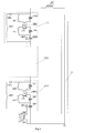
- Figure 1 depicts pictorial diagram of a single module
- Figure 2 gives a graphical representation of the output voltage pulse after bi-directional power switch operation up to the moment when maximum output voltage amplitude is reached.
- Setup includes single module (1), which includes three capacitors.
- the first input (1) is connected to the first terminal of the first capacitor (C11), on the other hand the second input of the module (1) is connected to the anode of the first diode (D11), which cathode is connected to the second terminal of the first capacitor (C11) and the firs terminal of the second capacitor (C21) and the first terminal of the second inductor (L21).
- the second terminal of the second inductor (L21) is connected to the collector terminal of the IGBT switch (T11) with additional diode (DT1) connected anti-parallel to the power switch (T11).
- the second terminal of the third capacitor (C31) is connected simultaneously with the first terminal of the third inductor (L31) and the anode of the second diode (D21) and states the first output of the module (1).
- the second terminal of the third inductor (L31) is connected to the anode of the third diode (DT1) and the emitter terminal of the IGBT switch (T11) and the second terminal of the second capacitor (C21), cathode of the second diode (D21) is connected with the first terminal of the first inductor (L11), the second terminal of the first inductor (L11) is connected to the first terminal of the of the first capacitor (C11).
- a pulse shaping circuitry (UKI) is shaping the power supply pulses of the module (1) with the means of supplying its primary side (Tr1).
- First output of the module (1) is connected to the first terminal of the non-linear choke (Lk), which second terminal is connected to the first terminal of the load (R).
- the second terminal of the load (R) is connected to the grounded terminal where also one of the terminals of the secondary transformer side (Tr2) is connected as well as the second terminal of the inductor (L11).
- Turning-on of the power switch (T11) through magnetically coupled inductors (L21) and (L31) to parallel connected capacitors (C21) and (C31) begins the process of resonant recharge that changes the polarity of the voltage across these capacitors and simultaneously connects all three capacitors (C11, C21, C31) in series.
- the output voltage of module (1) has a momentary negative value of a single capacitor voltage, while after the half-wave oscillation period it reaches the value of tripled initial voltage value of a single capacitor in the module.
- the first output of the first module (1) is connected to the first input of the second module (1), while the second output of the first module (1) is connected to the second input of the second module (1).
- the first output of the second module (1) is connected to the first input of the third module (1), while the second output of the second module (1) is connected to the second input of the third module (1).
- the first output of the third module (1) is connected to the first terminal of the non-linear choke (Lk), which second terminal is connected to the first terminal of the load (R).
- the second terminal of the load (R) is connected to the grounded terminal where also one of the terminals of the secondary transformer side (Tr2) is connected as well as the second terminal of the inductor (L 11) of the first module (1).
Abstract
Description
- The invention relates to method for shaping of high voltage pulse in generator module and high voltage generator setup aimed at, between other applications, plasma generation in high power reactor modules.
- In existing high voltage pulse generators based on Marx topology, as described in German Patent Description
DE455933 , the output voltage is equal to maximally the multiplication of number of modules used for construction while maximum voltage value of singular module is limited to maximum allowable switching element blocking voltage. The Fitch topology, as described in United States PatentsUS3366799 andUS3746881 ,US7209373 in conjunction with Marx topology allows to double the maximal voltage value while maintaining the same number of used modules. Recent developments of the solutions described above refer to simple replacement of switching elements as spark-gaps and thyratrons by semiconductor, solid state power switches as described in "Solid-state Marx Bank Modulator For the Next Linear Collider", proceedings of EPAC 2004, Lucerne, Switzerland. - According to present invention the method for shaping of high voltage pulse in a generator module comprise of voltage addition of serially connected, charged capacitors, characterized by the fact, that three initially charged capacitors are connected together, whereby in two of them, connected in parallel, the polarity is reversed in the process of resonant recharge through a bi-directional power switch that connects inductors and plurality of capacitors serially. In the moment of bi-directional, power switch operation output voltage obtains negative polarity in respect to wished output voltage, with the value equal to voltage across a single capacitor while after the resonant recharge process the voltage value is tripled. As a bi-directional power switch power transistor can be used however other switching devices meeting accepted requirements can be employed. In time intervals between consecutive bi-directional switch operation all capacitors are charged in a way, that overall output voltage of the module is equal to zero. It is possible as in this operating regime the second and third capacitor are connected in parallel and their polarity is in opposition with respect to the first capacitor. In the moment of switch operation two processes are initiated. The first process consists of resonant recharge of the second and third capacitor through the second and third inductor, profitably magnetically coupled as the voltage change dynamics across the second and third capacitor will be equal. The second process states the summarization of voltages across all three capacitors of the module. The effect of voltage summarization in the moment of switch operation results in momentary negative voltage with the initial value of a single capacitor voltage. The maximal output voltage value is reached after the entire recharge period of the second and third capacitor that is after the half-wave oscillation period and it reaches the value of tripled initial voltage value of a single capacitor in the module.
- High voltage generator setup, according to present invention, constructed of at least one module that includes plurality of capacitors, inductors and switching elements is characterized by the fact, that the module includes three capacitors. The first input of the module is connected with the first terminal of the first capacitor, on the other hand the second input of the module is connected to the anode of the first diode which cathode is connected to the second terminal of the first capacitor and the firs terminal of the second capacitor and the first terminal of the second inductor. The second output of the module consists of the second terminal of the second inductor connected to the first terminal of the bi-directional switch and simultaneously cathode of the of the third diode and the first terminal of the third capacitor. The second terminal of the third capacitor is connected simultaneously with the first terminal of the third inductor and the anode of the second diode and states the first output of the module. The second terminal of the third inductor is connected to the anode of the third diode and the second terminal of the bi-directional switch and the second terminal of the second capacitor. Cathode of the second diode is connected with the first terminal of the first inductor, the second terminal of the first inductor is connected to the first terminal of the of the first capacitor. Between the first and second input of the module the secondary side of the transformer is connected which primary side is put within a pulse shaping circuitry. First output of the module is connected to the first terminal of the non-linear choke, which second terminal is connected to the first terminal of the load. The second terminal of the load is connected to the grounded terminal where also one of the terminals of the secondary transformer side is connected as well as the second terminal of the first inductor. As a power switch in the described setup every switching element can be used, preferably a transistor with anti-parallel diode connected in parallel with the switch with reversed conduction direction. It is profitable to magnetically couple the second and third inductor. In the generator setup as invented the second and third capacitor are connected in parallel, and their voltage polarity is reversed with respect to the first capacitor. In the moment of switch operation two processes are initiated. The first process consists of resonant recharge of the second and third capacitor through the second and third inductor, profitably magnetically coupled as the voltage change dynamics across the second and third capacitor will be equal. The second process states the summarization of voltages across all three capacitors of the module. The effect of voltage summarization in the moment of switch operation results in momentary negative voltage with the initial value of a single capacitor voltage. The maximal output voltage value is reached after the entire recharge period of the second and third capacitor that is after the half-wave oscillation period and it reaches the value of tripled initial voltage value of a single capacitor in the module.
- It is profitable to implement a multi-module construction with consecutive modules connected in series where the first output of the previous module is connected to the first input of the following module, and the second output of the previous module is connected to the second input of the following module. It allows output voltage multiplication equal to the number of maximum voltage across a single module multiplied with the overall number of consecutive modules.
- Triple voltage multiplication across a single module allows higher overall voltage output when compared to other present solutions, which in practice enables lowering of the number of necessary modules. Initial negative voltage slope significantly lowers the time integral of the half-wave voltage oscillation period which enables output magnetic compression circuit magnetic core volume reduction.
- Invented means of voltage pulse shaping as well as invented generator setup are depicted in examples and on Figures, where
Figure 1 depicts pictorial diagram of a single module,Figure 2 gives a graphical representation of the output voltage pulse after bi-directional power switch operation up to the moment when maximum output voltage amplitude is reached. - Setup includes single module (1), which includes three capacitors. The first input (1) is connected to the first terminal of the first capacitor (C11), on the other hand the second input of the module (1) is connected to the anode of the first diode (D11), which cathode is connected to the second terminal of the first capacitor (C11) and the firs terminal of the second capacitor (C21) and the first terminal of the second inductor (L21). The second terminal of the second inductor (L21) is connected to the collector terminal of the IGBT switch (T11) with additional diode (DT1) connected anti-parallel to the power switch (T11). Simultaneously it is connected to the cathode of the of the third diode (DT1) and the first terminal of the third capacitor (C31). In this way the second output of the module (1) is created. The second terminal of the third capacitor (C31) is connected simultaneously with the first terminal of the third inductor (L31) and the anode of the second diode (D21) and states the first output of the module (1). The second terminal of the third inductor (L31) is connected to the anode of the third diode (DT1) and the emitter terminal of the IGBT switch (T11) and the second terminal of the second capacitor (C21), cathode of the second diode (D21) is connected with the first terminal of the first inductor (L11), the second terminal of the first inductor (L11) is connected to the first terminal of the of the first capacitor (C11). Between the first and second input of the module (1) the secondary side of the transformer (Tr2) is connected which primary side (Tr1) is put within a pulse shaping circuitry (UKI). The shape forming circuitry (UKI) is shaping the power supply pulses of the module (1) with the means of supplying its primary side (Tr1). First output of the module (1) is connected to the first terminal of the non-linear choke (Lk), which second terminal is connected to the first terminal of the load (R). The second terminal of the load (R) is connected to the grounded terminal where also one of the terminals of the secondary transformer side (Tr2) is connected as well as the second terminal of the inductor (L11).
Turning-on of the power switch (T11) through magnetically coupled inductors (L21) and (L31) to parallel connected capacitors (C21) and (C31) begins the process of resonant recharge that changes the polarity of the voltage across these capacitors and simultaneously connects all three capacitors (C11, C21, C31) in series. In the moment of switch (T11) operation the output voltage of module (1) has a momentary negative value of a single capacitor voltage, while after the half-wave oscillation period it reaches the value of tripled initial voltage value of a single capacitor in the module. - Setup as described in example 1 however made of three modules. The first output of the first module (1) is connected to the first input of the second module (1), while the second output of the first module (1) is connected to the second input of the second module (1). The first output of the second module (1) is connected to the first input of the third module (1), while the second output of the second module (1) is connected to the second input of the third module (1). The first output of the third module (1) is connected to the first terminal of the non-linear choke (Lk), which second terminal is connected to the first terminal of the load (R). The second terminal of the load (R) is connected to the grounded terminal where also one of the terminals of the secondary transformer side (Tr2) is connected as well as the second terminal of the inductor (L 11) of the first module (1).
Claims (7)
- The method for shaping of high voltage pulse in a generator module, based on summarization of voltages across serially connected capacitors, characterized in that it connects three initially charged capacitors, where two of them, connected in parallel change voltage polarity due to resonant recharge after bi-directional power switch operation, that connects to each of the capacitors recharge inductors and connects all three capacitors in series.
- The method according to claim 1, characterized in that as a bi-directional switch a power transistor or different switching element is used.
- The method according to claim 1, characterized in that magnetically coupled inductors are used.
- High voltage pulse generator setup, constructed of at least one module, including capacitors, inductors and a switching element, characterized in that the module includes three capacitors, where the first module input (1) is connected to the first terminal of the first capacitor (C11), on the other hand the second input of the module (1) is connected to the anode of the first diode (D11), which cathode is connected to the second terminal of the first capacitor (C11) and the firs terminal of the second capacitor (C21) and the first terminal of the second inductor (L21), and the second terminal of the second inductor (L21) is connected to the first terminal of the bi-directional switch (T11) and simultaneously it is connected to the cathode of the of the third diode (DT1) and the first terminal of the third capacitor (C31), this way the second output of the module (1) is created, and the second terminal of the third capacitor (C31) is connected simultaneously with the first terminal of the third inductor (L31) and the anode of the second diode (D21) and states the first output of the module (1), and the second terminal of the third inductor (L31) is connected to the anode of the third diode (DT1) and the second terminal of the bi-directional switch (T11) and the second terminal of the second capacitor (C21), cathode of the second diode (D21) is connected with the first terminal of the first inductor (L11), the second terminal of the first inductor (L11) is connected to the first terminal of the of the first capacitor (C11), and between the first and second input of the module (1) the secondary side of the transformer (Tr2) is connected which primary side (Tr1) is put within a pulse shaping circuitry (UKI), and first output of the module (1) is connected to the first terminal of the non-linear choke (Lk), which second terminal is connected to the first terminal of the load (R), and the second terminal of the load (R) is connected to the grounded terminal where also one of the terminals of the secondary transformer side (Tr2) is connected as well as the second terminal of the inductor (L11).
- Generator setup according to claim 4, characterized in that as the bi-directional switch a power transistor with anti-parallel diode is used.
- Generator setup according to claim 4, characterized in that inductors (L21) and (L31) are magnetically coupled.
- Setup according to any of the claims 4-7, characterized in that the first output of the previous module is connected to the first input of the following module and the second output of the previous module is connected to the second input of the following module.
Applications Claiming Priority (1)
| Application Number | Priority Date | Filing Date | Title |
|---|---|---|---|
| PL384795A PL213859B1 (en) | 2008-03-27 | 2008-03-27 | The manner of forming of high voltage impulse in generator's module and high voltage impulse in generator |
Publications (2)
| Publication Number | Publication Date |
|---|---|
| EP2106025A1 true EP2106025A1 (en) | 2009-09-30 |
| EP2106025B1 EP2106025B1 (en) | 2014-04-02 |
Family
ID=40757066
Family Applications (1)
| Application Number | Title | Priority Date | Filing Date |
|---|---|---|---|
| EP09460013.7A Active EP2106025B1 (en) | 2008-03-27 | 2009-03-17 | The method for shaping of high voltage pulse in a generator module and high voltage generator setup |
Country Status (2)
| Country | Link |
|---|---|
| EP (1) | EP2106025B1 (en) |
| PL (1) | PL213859B1 (en) |
Cited By (2)
| Publication number | Priority date | Publication date | Assignee | Title |
|---|---|---|---|---|
| CN102522964A (en) * | 2012-01-05 | 2012-06-27 | 哈尔滨工业大学 | Insulated gate bipolar transistor (IGBT) driving circuit for Marx high voltage generator |
| CN102594127A (en) * | 2012-03-02 | 2012-07-18 | 西安交通大学 | Repetition frequency compact pulse multiplier based on Fitch circuit |
Citations (9)
| Publication number | Priority date | Publication date | Assignee | Title |
|---|---|---|---|---|
| DE455933C (en) | 1923-10-12 | 1928-02-13 | Erwin Marx Dr Ing | Procedure for impact testing of insulators and other electrical devices |
| US3366799A (en) | 1963-10-10 | 1968-01-30 | Atomic Energy Authority Uk | Electrical pulse generators |
| US3746881A (en) | 1971-02-16 | 1973-07-17 | Maxwell Lab | Marx generator and triggering circuitry therefor |
| FR2495853A1 (en) * | 1980-05-05 | 1982-06-11 | Inst Vysokikh Temperatur Akade | Accelerator tube pulse transformer circuit - has primaries connected to commutated capacitors and secondaries with bifilar conductors connected to charge unit |
| EP0094765A2 (en) * | 1982-05-17 | 1983-11-23 | Unisys Corporation | Short pulse generator |
| US5105097A (en) * | 1991-02-01 | 1992-04-14 | Lasertechnics, Inc. | Passive magnetic switch for erecting multiple stage, high-pulse-rate voltage multipliers |
| US5561597A (en) * | 1992-04-06 | 1996-10-01 | D.C. Transformation, Inc. | Compact and efficient transformerless power conversion system |
| US7209373B2 (en) | 2004-12-28 | 2007-04-24 | Kaiser Systems, Inc. | High voltage pulse generator |
| US7307362B1 (en) * | 2002-02-06 | 2007-12-11 | Joseph Yampolsky | Solid-state microsecond capacitance charger for high voltage and pulsed power |
-
2008
- 2008-03-27 PL PL384795A patent/PL213859B1/en not_active IP Right Cessation
-
2009
- 2009-03-17 EP EP09460013.7A patent/EP2106025B1/en active Active
Patent Citations (9)
| Publication number | Priority date | Publication date | Assignee | Title |
|---|---|---|---|---|
| DE455933C (en) | 1923-10-12 | 1928-02-13 | Erwin Marx Dr Ing | Procedure for impact testing of insulators and other electrical devices |
| US3366799A (en) | 1963-10-10 | 1968-01-30 | Atomic Energy Authority Uk | Electrical pulse generators |
| US3746881A (en) | 1971-02-16 | 1973-07-17 | Maxwell Lab | Marx generator and triggering circuitry therefor |
| FR2495853A1 (en) * | 1980-05-05 | 1982-06-11 | Inst Vysokikh Temperatur Akade | Accelerator tube pulse transformer circuit - has primaries connected to commutated capacitors and secondaries with bifilar conductors connected to charge unit |
| EP0094765A2 (en) * | 1982-05-17 | 1983-11-23 | Unisys Corporation | Short pulse generator |
| US5105097A (en) * | 1991-02-01 | 1992-04-14 | Lasertechnics, Inc. | Passive magnetic switch for erecting multiple stage, high-pulse-rate voltage multipliers |
| US5561597A (en) * | 1992-04-06 | 1996-10-01 | D.C. Transformation, Inc. | Compact and efficient transformerless power conversion system |
| US7307362B1 (en) * | 2002-02-06 | 2007-12-11 | Joseph Yampolsky | Solid-state microsecond capacitance charger for high voltage and pulsed power |
| US7209373B2 (en) | 2004-12-28 | 2007-04-24 | Kaiser Systems, Inc. | High voltage pulse generator |
Non-Patent Citations (1)
| Title |
|---|
| "Solid-state Marx Bank Modulator For the Next Linear Collider", PROCEEDINGS OF EPAC, 2004 |
Cited By (3)
| Publication number | Priority date | Publication date | Assignee | Title |
|---|---|---|---|---|
| CN102522964A (en) * | 2012-01-05 | 2012-06-27 | 哈尔滨工业大学 | Insulated gate bipolar transistor (IGBT) driving circuit for Marx high voltage generator |
| CN102522964B (en) * | 2012-01-05 | 2014-07-30 | 哈尔滨工业大学 | Insulated gate bipolar transistor (IGBT) driving circuit for Marx high voltage generator |
| CN102594127A (en) * | 2012-03-02 | 2012-07-18 | 西安交通大学 | Repetition frequency compact pulse multiplier based on Fitch circuit |
Also Published As
| Publication number | Publication date |
|---|---|
| PL213859B1 (en) | 2013-05-31 |
| EP2106025B1 (en) | 2014-04-02 |
| PL384795A1 (en) | 2009-09-28 |
Similar Documents
| Publication | Publication Date | Title |
|---|---|---|
| US7209373B2 (en) | High voltage pulse generator | |
| CN101202511B (en) | Synchronous rectification circuit for resonance power converter | |
| US9577548B2 (en) | Power conversion for distributed DC source array | |
| CN113078840B (en) | Power supply circuit, repeated flat-top pulse high-intensity magnetic field generating device and control method thereof | |
| US7868485B2 (en) | Pulsed power supply with current ripple reduction | |
| CN109995265B (en) | Program-controlled high-voltage repetition frequency nanosecond pulse power supply, system and control method | |
| EP2475491A1 (en) | Energy conversion method and apparatus, and welding device | |
| EP2106025B1 (en) | The method for shaping of high voltage pulse in a generator module and high voltage generator setup | |
| CN103208936A (en) | Ac power supply apparatus | |
| CN113630107A (en) | Bipolar high-repetition-frequency high-voltage nanosecond pulse generation circuit and method | |
| CN102437773A (en) | Pulse generator | |
| CN101529708B (en) | Microwave transmission line DC/DC converter | |
| Eitzen et al. | Bidirectional power electronics for driving dielectric elastomer transducers | |
| Javali et al. | A new step-up DC-DC converter for isolated power system | |
| WO2006007274A1 (en) | Semiconductor switch assembly for pulse power apparatus | |
| CN102664606A (en) | Pulse generator | |
| CN115514212A (en) | Marx high-voltage pulse power supply based on high-gain boost DC-DC converter | |
| CN105391290B (en) | The controller and its operating method of residual current protection with diode | |
| US20050128656A1 (en) | Semiconductor switch pulse discharge module | |
| CN102647106A (en) | Pulse generator | |
| CN103684032A (en) | Composite pulse generation circuit | |
| JP4329415B2 (en) | Pulse power supply | |
| Kozasa et al. | Solid-state Marx generator for international linear collider | |
| Ni et al. | Transformer Selection Calculation for the design of Flyback Switching Power Supply | |
| CN106300927A (en) | Switching Power Supply modulation circuit and Switching Power Supply |
Legal Events
| Date | Code | Title | Description |
|---|---|---|---|
| PUAI | Public reference made under article 153(3) epc to a published international application that has entered the european phase |
Free format text: ORIGINAL CODE: 0009012 |
|
| AK | Designated contracting states |
Kind code of ref document: A1 Designated state(s): AT BE BG CH CY CZ DE DK EE ES FI FR GB GR HR HU IE IS IT LI LT LU LV MC MK MT NL NO PL PT RO SE SI SK TR |
|
| AX | Request for extension of the european patent |
Extension state: AL BA RS |
|
| 17P | Request for examination filed |
Effective date: 20091228 |
|
| 17Q | First examination report despatched |
Effective date: 20100128 |
|
| AKX | Designation fees paid |
Designated state(s): AT BE BG CH CY CZ DE DK EE ES FI FR GB GR HR HU IE IS IT LI LT LU LV MC MK MT NL NO PL PT RO SE SI SK TR |
|
| AXX | Extension fees paid |
Extension state: RS Payment date: 20091228 Extension state: BA Payment date: 20091228 Extension state: AL Payment date: 20091228 |
|
| GRAP | Despatch of communication of intention to grant a patent |
Free format text: ORIGINAL CODE: EPIDOSNIGR1 |
|
| INTG | Intention to grant announced |
Effective date: 20140107 |
|
| GRAS | Grant fee paid |
Free format text: ORIGINAL CODE: EPIDOSNIGR3 |
|
| GRAA | (expected) grant |
Free format text: ORIGINAL CODE: 0009210 |
|
| AK | Designated contracting states |
Kind code of ref document: B1 Designated state(s): AT BE BG CH CY CZ DE DK EE ES FI FR GB GR HR HU IE IS IT LI LT LU LV MC MK MT NL NO PL PT RO SE SI SK TR |
|
| AX | Request for extension of the european patent |
Extension state: AL BA RS |
|
| REG | Reference to a national code |
Ref country code: GB Ref legal event code: FG4D |
|
| REG | Reference to a national code |
Ref country code: AT Ref legal event code: REF Ref document number: 660662 Country of ref document: AT Kind code of ref document: T Effective date: 20140415 Ref country code: CH Ref legal event code: EP |
|
| REG | Reference to a national code |
Ref country code: IE Ref legal event code: FG4D |
|
| REG | Reference to a national code |
Ref country code: DE Ref legal event code: R096 Ref document number: 602009022919 Country of ref document: DE Effective date: 20140515 |
|
| REG | Reference to a national code |
Ref country code: AT Ref legal event code: MK05 Ref document number: 660662 Country of ref document: AT Kind code of ref document: T Effective date: 20140402 |
|
| REG | Reference to a national code |
Ref country code: NL Ref legal event code: VDEP Effective date: 20140402 |
|
| REG | Reference to a national code |
Ref country code: LT Ref legal event code: MG4D |
|
| PG25 | Lapsed in a contracting state [announced via postgrant information from national office to epo] |
Ref country code: NL Free format text: LAPSE BECAUSE OF FAILURE TO SUBMIT A TRANSLATION OF THE DESCRIPTION OR TO PAY THE FEE WITHIN THE PRESCRIBED TIME-LIMIT Effective date: 20140402 Ref country code: BG Free format text: LAPSE BECAUSE OF FAILURE TO SUBMIT A TRANSLATION OF THE DESCRIPTION OR TO PAY THE FEE WITHIN THE PRESCRIBED TIME-LIMIT Effective date: 20140702 Ref country code: LT Free format text: LAPSE BECAUSE OF FAILURE TO SUBMIT A TRANSLATION OF THE DESCRIPTION OR TO PAY THE FEE WITHIN THE PRESCRIBED TIME-LIMIT Effective date: 20140402 Ref country code: FI Free format text: LAPSE BECAUSE OF FAILURE TO SUBMIT A TRANSLATION OF THE DESCRIPTION OR TO PAY THE FEE WITHIN THE PRESCRIBED TIME-LIMIT Effective date: 20140402 Ref country code: NO Free format text: LAPSE BECAUSE OF FAILURE TO SUBMIT A TRANSLATION OF THE DESCRIPTION OR TO PAY THE FEE WITHIN THE PRESCRIBED TIME-LIMIT Effective date: 20140702 Ref country code: CZ Free format text: LAPSE BECAUSE OF FAILURE TO SUBMIT A TRANSLATION OF THE DESCRIPTION OR TO PAY THE FEE WITHIN THE PRESCRIBED TIME-LIMIT Effective date: 20140402 Ref country code: GR Free format text: LAPSE BECAUSE OF FAILURE TO SUBMIT A TRANSLATION OF THE DESCRIPTION OR TO PAY THE FEE WITHIN THE PRESCRIBED TIME-LIMIT Effective date: 20140703 Ref country code: IS Free format text: LAPSE BECAUSE OF FAILURE TO SUBMIT A TRANSLATION OF THE DESCRIPTION OR TO PAY THE FEE WITHIN THE PRESCRIBED TIME-LIMIT Effective date: 20140802 Ref country code: CY Free format text: LAPSE BECAUSE OF FAILURE TO SUBMIT A TRANSLATION OF THE DESCRIPTION OR TO PAY THE FEE WITHIN THE PRESCRIBED TIME-LIMIT Effective date: 20140402 |
|
| PG25 | Lapsed in a contracting state [announced via postgrant information from national office to epo] |
Ref country code: PL Free format text: LAPSE BECAUSE OF FAILURE TO SUBMIT A TRANSLATION OF THE DESCRIPTION OR TO PAY THE FEE WITHIN THE PRESCRIBED TIME-LIMIT Effective date: 20140402 Ref country code: ES Free format text: LAPSE BECAUSE OF FAILURE TO SUBMIT A TRANSLATION OF THE DESCRIPTION OR TO PAY THE FEE WITHIN THE PRESCRIBED TIME-LIMIT Effective date: 20140402 Ref country code: LV Free format text: LAPSE BECAUSE OF FAILURE TO SUBMIT A TRANSLATION OF THE DESCRIPTION OR TO PAY THE FEE WITHIN THE PRESCRIBED TIME-LIMIT Effective date: 20140402 Ref country code: AT Free format text: LAPSE BECAUSE OF FAILURE TO SUBMIT A TRANSLATION OF THE DESCRIPTION OR TO PAY THE FEE WITHIN THE PRESCRIBED TIME-LIMIT Effective date: 20140402 Ref country code: HR Free format text: LAPSE BECAUSE OF FAILURE TO SUBMIT A TRANSLATION OF THE DESCRIPTION OR TO PAY THE FEE WITHIN THE PRESCRIBED TIME-LIMIT Effective date: 20140402 Ref country code: SE Free format text: LAPSE BECAUSE OF FAILURE TO SUBMIT A TRANSLATION OF THE DESCRIPTION OR TO PAY THE FEE WITHIN THE PRESCRIBED TIME-LIMIT Effective date: 20140402 |
|
| PG25 | Lapsed in a contracting state [announced via postgrant information from national office to epo] |
Ref country code: PT Free format text: LAPSE BECAUSE OF FAILURE TO SUBMIT A TRANSLATION OF THE DESCRIPTION OR TO PAY THE FEE WITHIN THE PRESCRIBED TIME-LIMIT Effective date: 20140804 |
|
| REG | Reference to a national code |
Ref country code: DE Ref legal event code: R097 Ref document number: 602009022919 Country of ref document: DE |
|
| PG25 | Lapsed in a contracting state [announced via postgrant information from national office to epo] |
Ref country code: RO Free format text: LAPSE BECAUSE OF FAILURE TO SUBMIT A TRANSLATION OF THE DESCRIPTION OR TO PAY THE FEE WITHIN THE PRESCRIBED TIME-LIMIT Effective date: 20140402 Ref country code: SK Free format text: LAPSE BECAUSE OF FAILURE TO SUBMIT A TRANSLATION OF THE DESCRIPTION OR TO PAY THE FEE WITHIN THE PRESCRIBED TIME-LIMIT Effective date: 20140402 Ref country code: DK Free format text: LAPSE BECAUSE OF FAILURE TO SUBMIT A TRANSLATION OF THE DESCRIPTION OR TO PAY THE FEE WITHIN THE PRESCRIBED TIME-LIMIT Effective date: 20140402 Ref country code: BE Free format text: LAPSE BECAUSE OF FAILURE TO SUBMIT A TRANSLATION OF THE DESCRIPTION OR TO PAY THE FEE WITHIN THE PRESCRIBED TIME-LIMIT Effective date: 20140402 Ref country code: EE Free format text: LAPSE BECAUSE OF FAILURE TO SUBMIT A TRANSLATION OF THE DESCRIPTION OR TO PAY THE FEE WITHIN THE PRESCRIBED TIME-LIMIT Effective date: 20140402 |
|
| PLBE | No opposition filed within time limit |
Free format text: ORIGINAL CODE: 0009261 |
|
| STAA | Information on the status of an ep patent application or granted ep patent |
Free format text: STATUS: NO OPPOSITION FILED WITHIN TIME LIMIT |
|
| 26N | No opposition filed |
Effective date: 20150106 |
|
| PG25 | Lapsed in a contracting state [announced via postgrant information from national office to epo] |
Ref country code: IT Free format text: LAPSE BECAUSE OF FAILURE TO SUBMIT A TRANSLATION OF THE DESCRIPTION OR TO PAY THE FEE WITHIN THE PRESCRIBED TIME-LIMIT Effective date: 20140402 |
|
| REG | Reference to a national code |
Ref country code: DE Ref legal event code: R097 Ref document number: 602009022919 Country of ref document: DE Effective date: 20150106 |
|
| PG25 | Lapsed in a contracting state [announced via postgrant information from national office to epo] |
Ref country code: SI Free format text: LAPSE BECAUSE OF FAILURE TO SUBMIT A TRANSLATION OF THE DESCRIPTION OR TO PAY THE FEE WITHIN THE PRESCRIBED TIME-LIMIT Effective date: 20140402 |
|
| REG | Reference to a national code |
Ref country code: DE Ref legal event code: R119 Ref document number: 602009022919 Country of ref document: DE |
|
| PG25 | Lapsed in a contracting state [announced via postgrant information from national office to epo] |
Ref country code: MC Free format text: LAPSE BECAUSE OF FAILURE TO SUBMIT A TRANSLATION OF THE DESCRIPTION OR TO PAY THE FEE WITHIN THE PRESCRIBED TIME-LIMIT Effective date: 20140402 Ref country code: LU Free format text: LAPSE BECAUSE OF FAILURE TO SUBMIT A TRANSLATION OF THE DESCRIPTION OR TO PAY THE FEE WITHIN THE PRESCRIBED TIME-LIMIT Effective date: 20150317 |
|
| REG | Reference to a national code |
Ref country code: CH Ref legal event code: PL |
|
| GBPC | Gb: european patent ceased through non-payment of renewal fee |
Effective date: 20150317 |
|
| REG | Reference to a national code |
Ref country code: FR Ref legal event code: ST Effective date: 20151130 |
|
| REG | Reference to a national code |
Ref country code: IE Ref legal event code: MM4A |
|
| PG25 | Lapsed in a contracting state [announced via postgrant information from national office to epo] |
Ref country code: IE Free format text: LAPSE BECAUSE OF NON-PAYMENT OF DUE FEES Effective date: 20150317 Ref country code: GB Free format text: LAPSE BECAUSE OF NON-PAYMENT OF DUE FEES Effective date: 20150317 Ref country code: DE Free format text: LAPSE BECAUSE OF NON-PAYMENT OF DUE FEES Effective date: 20151001 Ref country code: CH Free format text: LAPSE BECAUSE OF NON-PAYMENT OF DUE FEES Effective date: 20150331 Ref country code: LI Free format text: LAPSE BECAUSE OF NON-PAYMENT OF DUE FEES Effective date: 20150331 |
|
| PG25 | Lapsed in a contracting state [announced via postgrant information from national office to epo] |
Ref country code: FR Free format text: LAPSE BECAUSE OF NON-PAYMENT OF DUE FEES Effective date: 20150331 |
|
| PG25 | Lapsed in a contracting state [announced via postgrant information from national office to epo] |
Ref country code: MT Free format text: LAPSE BECAUSE OF FAILURE TO SUBMIT A TRANSLATION OF THE DESCRIPTION OR TO PAY THE FEE WITHIN THE PRESCRIBED TIME-LIMIT Effective date: 20140402 |
|
| PG25 | Lapsed in a contracting state [announced via postgrant information from national office to epo] |
Ref country code: HU Free format text: LAPSE BECAUSE OF FAILURE TO SUBMIT A TRANSLATION OF THE DESCRIPTION OR TO PAY THE FEE WITHIN THE PRESCRIBED TIME-LIMIT; INVALID AB INITIO Effective date: 20090317 |
|
| PG25 | Lapsed in a contracting state [announced via postgrant information from national office to epo] |
Ref country code: TR Free format text: LAPSE BECAUSE OF FAILURE TO SUBMIT A TRANSLATION OF THE DESCRIPTION OR TO PAY THE FEE WITHIN THE PRESCRIBED TIME-LIMIT Effective date: 20140402 |
|
| PG25 | Lapsed in a contracting state [announced via postgrant information from national office to epo] |
Ref country code: MK Free format text: LAPSE BECAUSE OF FAILURE TO SUBMIT A TRANSLATION OF THE DESCRIPTION OR TO PAY THE FEE WITHIN THE PRESCRIBED TIME-LIMIT Effective date: 20140402 |