EP2105961A2 - Method and system for inter-chip communication via package waveguides - Google Patents
Method and system for inter-chip communication via package waveguides Download PDFInfo
- Publication number
- EP2105961A2 EP2105961A2 EP09004461A EP09004461A EP2105961A2 EP 2105961 A2 EP2105961 A2 EP 2105961A2 EP 09004461 A EP09004461 A EP 09004461A EP 09004461 A EP09004461 A EP 09004461A EP 2105961 A2 EP2105961 A2 EP 2105961A2
- Authority
- EP
- European Patent Office
- Prior art keywords
- waveguides
- layer package
- integrated
- signals
- package
- Prior art date
- Legal status (The legal status is an assumption and is not a legal conclusion. Google has not performed a legal analysis and makes no representation as to the accuracy of the status listed.)
- Withdrawn
Links
Images



Classifications
-
- H—ELECTRICITY
- H10—SEMICONDUCTOR DEVICES; ELECTRIC SOLID-STATE DEVICES NOT OTHERWISE PROVIDED FOR
- H10W—GENERIC PACKAGES, INTERCONNECTIONS, CONNECTORS OR OTHER CONSTRUCTIONAL DETAILS OF DEVICES COVERED BY CLASS H10
- H10W90/00—Package configurations
- H10W90/701—Package configurations characterised by the relative positions of pads or connectors relative to package parts
-
- H—ELECTRICITY
- H10—SEMICONDUCTOR DEVICES; ELECTRIC SOLID-STATE DEVICES NOT OTHERWISE PROVIDED FOR
- H10W—GENERIC PACKAGES, INTERCONNECTIONS, CONNECTORS OR OTHER CONSTRUCTIONAL DETAILS OF DEVICES COVERED BY CLASS H10
- H10W44/00—Electrical arrangements for controlling or matching impedance
- H10W44/20—Electrical arrangements for controlling or matching impedance at high-frequency [HF] or radio frequency [RF]
-
- H—ELECTRICITY
- H10—SEMICONDUCTOR DEVICES; ELECTRIC SOLID-STATE DEVICES NOT OTHERWISE PROVIDED FOR
- H10W—GENERIC PACKAGES, INTERCONNECTIONS, CONNECTORS OR OTHER CONSTRUCTIONAL DETAILS OF DEVICES COVERED BY CLASS H10
- H10W70/00—Package substrates; Interposers; Redistribution layers [RDL]
- H10W70/60—Insulating or insulated package substrates; Interposers; Redistribution layers
- H10W70/611—Insulating or insulated package substrates; Interposers; Redistribution layers for connecting multiple chips together
-
- H—ELECTRICITY
- H10—SEMICONDUCTOR DEVICES; ELECTRIC SOLID-STATE DEVICES NOT OTHERWISE PROVIDED FOR
- H10W—GENERIC PACKAGES, INTERCONNECTIONS, CONNECTORS OR OTHER CONSTRUCTIONAL DETAILS OF DEVICES COVERED BY CLASS H10
- H10W70/00—Package substrates; Interposers; Redistribution layers [RDL]
- H10W70/60—Insulating or insulated package substrates; Interposers; Redistribution layers
- H10W70/67—Insulating or insulated package substrates; Interposers; Redistribution layers characterised by their insulating layers or insulating parts
- H10W70/68—Shapes or dispositions thereof
- H10W70/685—Shapes or dispositions thereof comprising multiple insulating layers
-
- H—ELECTRICITY
- H10—SEMICONDUCTOR DEVICES; ELECTRIC SOLID-STATE DEVICES NOT OTHERWISE PROVIDED FOR
- H10W—GENERIC PACKAGES, INTERCONNECTIONS, CONNECTORS OR OTHER CONSTRUCTIONAL DETAILS OF DEVICES COVERED BY CLASS H10
- H10W90/00—Package configurations
-
- H—ELECTRICITY
- H10—SEMICONDUCTOR DEVICES; ELECTRIC SOLID-STATE DEVICES NOT OTHERWISE PROVIDED FOR
- H10W—GENERIC PACKAGES, INTERCONNECTIONS, CONNECTORS OR OTHER CONSTRUCTIONAL DETAILS OF DEVICES COVERED BY CLASS H10
- H10W44/00—Electrical arrangements for controlling or matching impedance
- H10W44/20—Electrical arrangements for controlling or matching impedance at high-frequency [HF] or radio frequency [RF]
- H10W44/203—Electrical connections
- H10W44/216—Waveguides, e.g. strip lines
-
- H—ELECTRICITY
- H10—SEMICONDUCTOR DEVICES; ELECTRIC SOLID-STATE DEVICES NOT OTHERWISE PROVIDED FOR
- H10W—GENERIC PACKAGES, INTERCONNECTIONS, CONNECTORS OR OTHER CONSTRUCTIONAL DETAILS OF DEVICES COVERED BY CLASS H10
- H10W44/00—Electrical arrangements for controlling or matching impedance
- H10W44/20—Electrical arrangements for controlling or matching impedance at high-frequency [HF] or radio frequency [RF]
- H10W44/255—Electrical arrangements for controlling or matching impedance at high-frequency [HF] or radio frequency [RF] for operation at multiple different frequencies
-
- H—ELECTRICITY
- H10—SEMICONDUCTOR DEVICES; ELECTRIC SOLID-STATE DEVICES NOT OTHERWISE PROVIDED FOR
- H10W—GENERIC PACKAGES, INTERCONNECTIONS, CONNECTORS OR OTHER CONSTRUCTIONAL DETAILS OF DEVICES COVERED BY CLASS H10
- H10W72/00—Interconnections or connectors in packages
- H10W72/071—Connecting or disconnecting
- H10W72/072—Connecting or disconnecting of bump connectors
-
- H—ELECTRICITY
- H10—SEMICONDUCTOR DEVICES; ELECTRIC SOLID-STATE DEVICES NOT OTHERWISE PROVIDED FOR
- H10W—GENERIC PACKAGES, INTERCONNECTIONS, CONNECTORS OR OTHER CONSTRUCTIONAL DETAILS OF DEVICES COVERED BY CLASS H10
- H10W72/00—Interconnections or connectors in packages
- H10W72/071—Connecting or disconnecting
- H10W72/073—Connecting or disconnecting of die-attach connectors
-
- H—ELECTRICITY
- H10—SEMICONDUCTOR DEVICES; ELECTRIC SOLID-STATE DEVICES NOT OTHERWISE PROVIDED FOR
- H10W—GENERIC PACKAGES, INTERCONNECTIONS, CONNECTORS OR OTHER CONSTRUCTIONAL DETAILS OF DEVICES COVERED BY CLASS H10
- H10W72/00—Interconnections or connectors in packages
- H10W72/20—Bump connectors, e.g. solder bumps or copper pillars; Dummy bumps; Thermal bumps
- H10W72/251—Materials
- H10W72/252—Materials comprising solid metals or solid metalloids, e.g. PbSn, Ag or Cu
-
- H—ELECTRICITY
- H10—SEMICONDUCTOR DEVICES; ELECTRIC SOLID-STATE DEVICES NOT OTHERWISE PROVIDED FOR
- H10W—GENERIC PACKAGES, INTERCONNECTIONS, CONNECTORS OR OTHER CONSTRUCTIONAL DETAILS OF DEVICES COVERED BY CLASS H10
- H10W74/00—Encapsulations, e.g. protective coatings
- H10W74/10—Encapsulations, e.g. protective coatings characterised by their shape or disposition
- H10W74/15—Encapsulations, e.g. protective coatings characterised by their shape or disposition on active surfaces of flip-chip devices, e.g. underfills
-
- H—ELECTRICITY
- H10—SEMICONDUCTOR DEVICES; ELECTRIC SOLID-STATE DEVICES NOT OTHERWISE PROVIDED FOR
- H10W—GENERIC PACKAGES, INTERCONNECTIONS, CONNECTORS OR OTHER CONSTRUCTIONAL DETAILS OF DEVICES COVERED BY CLASS H10
- H10W90/00—Package configurations
- H10W90/701—Package configurations characterised by the relative positions of pads or connectors relative to package parts
- H10W90/721—Package configurations characterised by the relative positions of pads or connectors relative to package parts of bump connectors
- H10W90/724—Package configurations characterised by the relative positions of pads or connectors relative to package parts of bump connectors between a chip and a stacked insulating package substrate, interposer or RDL
-
- H—ELECTRICITY
- H10—SEMICONDUCTOR DEVICES; ELECTRIC SOLID-STATE DEVICES NOT OTHERWISE PROVIDED FOR
- H10W—GENERIC PACKAGES, INTERCONNECTIONS, CONNECTORS OR OTHER CONSTRUCTIONAL DETAILS OF DEVICES COVERED BY CLASS H10
- H10W90/00—Package configurations
- H10W90/701—Package configurations characterised by the relative positions of pads or connectors relative to package parts
- H10W90/731—Package configurations characterised by the relative positions of pads or connectors relative to package parts of die-attach connectors
- H10W90/734—Package configurations characterised by the relative positions of pads or connectors relative to package parts of die-attach connectors between a chip and a stacked insulating package substrate, interposer or RDL
Definitions
- Certain embodiments of the invention relate to wireless communication. More specifically, certain embodiments of the invention relate to a method and system for inter-chip communication via integrated circuit package waveguides.
- Mobile communications have changed the way people communicate and mobile phones have been transformed from a luxury item to an essential part of every day life.
- the use of mobile phones is today dictated by social situations, rather than hampered by location or technology.
- voice connections fulfill the basic need to communicate, and mobile voice connections continue to filter even further into the fabric of every day life, the mobile Internet is the next step in the mobile communication revolution.
- the mobile Internet is poised to become a common source of everyday information, and easy, versatile mobile access to this data will be taken for granted.
- a method for wireless communication comprising:
- FIG. 1 is a block diagram of an exemplary wireless system, which may be utilized in accordance with an embodiment of the invention.
- FIG. 2A is a block diagram illustrating a cross-sectional view of a multi-layer package with waveguides, in accordance with an embodiment of the invention.
- FIG. 2B is a block diagram illustrating a cross-sectional view of a multi-layer package with embedded waveguides, in accordance with an embodiment of the invention.
- FIG. 3 is a block diagram illustrating a cross-sectional view of coplanar waveguides, in accordance with an embodiment of the invention.
- FIG. 4 is a block diagram illustrating exemplary inter-chip communication via waveguides integrated in a multi-layer package, in accordance with an embodiment of the invention.
- Certain aspects of the invention may be found in a method and system for inter-chip communication via integrated circuit package waveguides.
- Exemplary aspects of the invention may comprise communicating one or more signals between or among a plurality of integrated circuits via one or more waveguides integrated in a multi-layer package.
- the integrated circuits may be bonded to the multi-layer package.
- the waveguides may be configured via switches in the integrated circuits or by MEMS switches integrated in the multi-layer package.
- the signals may comprise a microwave signal and a low frequency control signal that may configure the microwave signal.
- the low frequency control signal may comprise a digital signal.
- the waveguides may comprise metal and/or semiconductor layers deposited on and/or embedded within the multi-layer package.
- FIG. 1 is a block diagram of an exemplary wireless system, which may be utilized in accordance with an embodiment of the invention.
- the wireless system 150 may comprise an antenna 151, a system memory 158, a logic block 160, and a multi-layer package 164.
- the multi-layer package 164 may comprise a chip 1 166, a chip 2 168, waveguides 170A, 170B, 170C, 170D, and 170E, a chip 3 172, a chip 4 174, a chip 5 176, and a chip 6 178.
- the chip 1 166 may comprise a baseband processor 154 and a processor 156, and the chip 2 168 may comprise a transceiver 152.
- the chip 3 172, chip 4 174, chip 5 176, and chip 6 178 may comprise circuitry for any functions of the wireless system 150.
- the invention may not be limited to the number of chips and waveguides shown in FIG. 1 . Any number of components and/or arrangements of circuitry may be integrated on any particular chip bonded to the multi-layer package 164, and any number of waveguides may be integrated within the multi-layer package 164 to enable communication between chips as defined by space on the multi-layer package 164 and the functional requirements of the wireless system 150.
- the antenna 151 may be used for reception and/or transmission of RF signals.
- the transceiver 152 may comprise suitable logic, circuitry, and/or code that may be enabled to modulate and upconvert baseband signals to RF signals for transmission by one or more antennas, which may be represented generically by the antenna 151.
- the transceiver 152 may also be enabled to downconvert and demodulate received RF signals to baseband signals.
- the RF signals may be received by one or more antennas, which may be represented generically by the antenna 151. Different wireless systems may use different antennas for transmission and reception.
- the transceiver 152 may be enabled to execute other functions, for example, filtering, coupling, and/or amplifying the baseband and/or RF signals. Although a single transceiver 152 is shown, the invention is not so limited.
- the transceiver 152 may be implemented as a separate transmitter and a separate receiver.
- the plurality of transceivers, transmitters and/or receivers may enable the wireless system 150 to handle a plurality of wireless protocols and/or standards including cellular, WLAN and PAN.
- the multi-layer package 164 may comprise multiple layers of insulator and conductive material for integrating multiple devices within the package.
- the multi-layer package 164 may enable the coupling of multiple devices to one or more integrated circuits, or chips.
- integrated circuits may be flip-chip bonded to the multi-layer package 164.
- devices integrated into the multi-layer package 164 may be coupled to devices within an integrated circuit with low parasitic impedances.
- One or more waveguides, such as the waveguides 170A-170E may enable communication between the chips.
- the waveguides 170A-170E may comprise suitable circuitry, logic and/or code that may enable the communication of electromagnetic signals between devices on and/or integrated within the multi-layer package 164.
- the waveguides 170A-170E may be configured to communicate at a specific frequency, 60 GHz or greater, for example, while still allowing low frequency control signals to propagate between devices.
- the control signals may allow setup, configuration and management of the microwave signal communication in the wireless system 150, for example.
- the baseband processor 154 may comprise suitable logic, circuitry, and/or code that may be enabled to process baseband signals for transmission via the transceiver 152 and/or the baseband signals received from the transceiver 152.
- the processor 156 may be any suitable processor or controller such as a CPU or DSP, or any type of integrated circuit processor.
- the processor 156 may comprise suitable logic, circuitry, and/or code that may be enabled to control the operations of the transceiver 152 and/or the baseband processor 154.
- the processor 156 may be utilized to update and/or modify programmable parameters and/or values in a plurality of components, devices, and/or processing elements in the transceiver 152 and/or the baseband processor 154. At least a portion of the programmable parameters may be stored in the system memory 158.
- the system memory 158 may comprise suitable logic, circuitry, and/or code that may be enabled to store a plurality of control and/or data information, including parameters needed to calculate frequencies and/or gain, and/or the frequency value and/or gain value.
- the system memory 158 may store at least a portion of the programmable parameters that may be manipulated by the processor 156.
- the logic block 160 may comprise suitable logic, circuitry, and/or code that may enable controlling of various functionalities of the wireless system 150.
- the logic block 160 may comprise one or more state machines that may generate signals to control the transceiver 152 and/or the baseband processor 154.
- the logic block 160 may also comprise registers that may hold data for controlling, for example, the transceiver 152 and/or the baseband processor 154.
- the logic block 160 may also generate and/or store status information that may be read by, for example, the processor 156.
- Amplifier gains and/or filtering characteristics, for example, may be controlled by the logic block 160.
- control and/or data information which may comprise the programmable parameters, may be transferred from other portions of the wireless system 150, not shown in FIG. 1 , to the processor 156.
- the processor 156 may be enabled to transfer control and/or data information, which may include the programmable parameters, to other portions of the wireless system 150, not shown in FIG. 1 , which may be part of the wireless system 150.
- the processor 156 may utilize the received control and/or data information, which may comprise the programmable parameters, to determine an operating mode of the transceiver 152. For example, the processor 156 may be utilized to select a specific frequency for a local oscillator, a specific gain for a variable gain amplifier, configure the local oscillator and/or configure the variable gain amplifier for operation in accordance with various embodiments of the invention. In an embodiment of the invention, the processor 156 may configure the waveguides 170A-170E to communicate signals of a desired frequency, 60 GHz or higher, for example, between the chips.
- low frequency, or out-of-band control signals such as a system management bus (SMBus) signal, for example, may also be communicated via the waveguide 170.
- the low-frequency wire interfaces may be used to improve Bluetooth-WLAN coexistence and/or antenna sharing in some instances.
- the 3-wire interface for example, may be used for Bluetooth-WLAN coexistence, in accordance with the IEEE 802.15.2 Recommended Practice.
- the 2-wire and 3-wire interface techniques may not permit the transmission of sophisticated data management data to a centralized management device and may be limited to blocking the resource access of one device while a transmission, for example, may be taking place on the other device.
- the specific frequency selected and/or parameters needed to calculate the specific frequency, and/or the specific gain value and/or the parameters, which may be utilized to calculate the specific gain may be stored in the system memory 158 via the processor 156, for example.
- the information stored in system memory 158 may be transferred to the transceiver 152 from the system memory 158 via the processor 156.
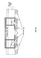
- FIG. 2A is a block diagram illustrating a cross-sectional view of a multi-layer package with waveguides, in accordance with an embodiment of the invention.
- chips 201A and 201 B there is shown chips 201A and 201 B, an insulating layer 203, metal layers 205A, 205B, 209A, and 209B, solder balls 211, a multi-layer package 213, and thermal epoxy 221.
- the chips 201A and 201 B may comprise one or more components and/or systems within the wireless system 150.
- the chips 201A and 201 B may be bump-bonded or flip-chip bonded to the multi-layer package 213 utilizing the solder balls 211.
- wire bonds connecting the chips 201A and 201 B to the multi-layer package 213 may be eliminated, thereby reducing and/or eliminating uncontrollable stray inductances due to wire bonds, for example.
- the thermal conductance out of the chip 201 may be greatly improved utilizing the solder balls 211 and the thermal epoxy 221.
- the thermal epoxy 221 may be electrically insulating but thermally conductive to allow for thermal energy to be conducted out of the chips 201A and 201 B to the much larger thermal mass of the multilayer package 213.
- the metal layers 205A, 205B, 209A, and 209B may comprise deposited metal layers utilized to delineate waveguides and other devices.
- the metal layers 209A, and 209B may be patterned such that they may comprise waveguides that may be utilized to communicate signal between chips coupled to the multi-layer package 213, such as the chips 201A and 201 B.
- the metal layers 209A and 209B may comprise a coplanar waveguide structure.
- the insulating layer 203 may comprise a layer of resistive material that may provide electrical isolation between the metal layers 209A and 209B and other layers and/or devices in the multi-layer package 213.
- one or more of the metal layers may comprise ferromagnetic and/or ferrimagnetic layers utilized to define devices such as transformers, inductors, baluns, isolators, circulators, and gyrators.
- the metal layers 205A, 205B, and 205C may provide electrical contact from the waveguide comprising the metal layers 209A and 209B and the chips 201A and 201 B via the solder balls 211.
- the number of metal layers may not be limited to the number of metal layers 205A, 205B, 205C, 209A, and 209B shown in FIG. 2 . Accordingly, there may be any number of layers embedded within and/or on the multi-layer package 213, depending on the number of contacts on the chips 201A and 201 B coupled to the solder balls 211, and the number of waveguides and other devices fabricated within and/or on the multi-layer package 213.
- the solder balls 211 may comprise spherical balls of metal to provide electrical, thermal and physical contact between the chips 201A and 201 B and the multi-layer package 213. In making the contact with the solder balls 211, the chips may be pressed with enough force to squash the metal spheres somewhat, and may be performed at an elevated temperature to provide suitable electrical resistance and physical bond strength.
- the thermal epoxy 221 may fill the volume between the solder balls 211 and may provide a high thermal conductance path for heat transfer out of the chips 201A and 201 B.
- the solder balls 211 may also be utilized to provide electrical, thermal and physical contact between the multi-layer package 213 and a printed circuit board comprising other parts of the wireless system 150, described with respect to FIG. 1 .
- the chips 201A and 201 B may comprise an RF front end, such as the RF transceiver 152, described with respect to FIG. 1 , and may be utilized to transmit and receive RF signals.
- the chips 201A and 201 B may be electrically coupled to the multi-layer package 213 and may communicate via waveguides integrated on the multi-layer package 213. Heat from the chips 201A and 201 B may be conducted to the multi-layer package 213 via the thermal epoxy 221 and the solder balls 211.
- a processor such as the processer 156 described with respect to FIG.
- the waveguide 1 may configure the waveguide comprising the metal layers 209A and 209B such that the chips 201A and 201B may communicate via the waveguide, providing a high frequency signal path, 60 GHz or higher, for example, as well as providing a path for low frequency control signals for the chips 201A and 201 B.
- the low frequency control signals may comprise 3-wire signal signals comprising clock and data streams, for example.
- the waveguides comprising the metal layers 209A and 209B may be configured by adjusting the length of the structures, and may be configurable via switches in the chips 201A and/or 201B and/or MEMS switches integrated in the multi-layer package 213. In this manner, the communication parameters of waveguides integrated into the multi-layer package may be configured for a plurality of applications.
- the metal layers 209A and 209B may be deposited on the same side of the multi-layer package 213, such that the metal layers 205A and 205B may not be needed to couple the waveguide to the chips 201A and 201 B.
- FIG. 2B is a block diagram illustrating a cross-sectional view of a multi-layer package with embedded waveguides, in accordance with an embodiment of the invention.
- FIG. 2A there is shown the chips 201A and 201 B, metal layers 205A, 205B, 215A, and 215B, the solder balls 211, the multi-layer package 213, the insulating layer 217, and thermal epoxy 221.
- the structure shown in FIG. 2B is substantially similar to that in FIG. 2A , except that the waveguide comprising the metal layers 215A and 215B may be embedded within the multi-layer package 213.
- a length of the metal layers 205A and 205B may be reduced, thereby reducing stray impedances, for example.
- integrating the metal layers 215A and 215B may allow more space for other components on the surface of the multi-layer package 213.
- the insulating layer 217 may comprise a layer of resistive material that may provide electrical isolation between the metal layers 215A and 215B and other layers and/or devices in the multi-layer package 213.
- the chips 201A and 201 B may comprise an RF front end, such as the RF transceiver 152, described with respect to FIG. 1 , and may be utilized to transmit and receive RF signals.
- the chips 201A and 201 B may be electrically coupled to the multi-layer package 213 and may communicate via one or more waveguides integrated within the multi-layer package 213. Heat from the chips 201A and 201 B may be conducted to the multi-layer package 213 via the thermal epoxy 221 and the solder balls 211.
- a processor such as the processer 156 described with respect to FIG.
- the waveguide 1 may configure the waveguide comprising the metal layers 215A and 215B such that the chips 201A and 201B may communicate via the waveguide, providing a high frequency signal path, 60 GHz or higher, for example, as well as providing a path for low frequency control signals for the chips 201A and 201 B.
- the low frequency control signals may comprise 3-wire signal signals comprising clock and data streams, for example.
- the waveguides within the metal layers 215A and 215B may be configured by adjusting the length of the structures, and may be configurable via switches in the chips 201A and/or 201B and/or MEMS switches integrated in the multi-layer package 213. In this manner, the communication parameters of waveguides integrated into the multi-layer package may be configured for a plurality of applications.
- FIG. 3 is a block diagram illustrating a cross-sectional view of coplanar waveguides, in accordance with an embodiment of the invention.
- coplanar waveguides comprising the metal layers 209A, 209B and the insulating layer 203 and also the metal layers 215A and 215B and the insulating layer 217, described with respect to FIGS. 2A and 2B , and the field lines 310.
- the metal layers 209A/209B and 215A/215B may comprise signals lines for the waveguides, and the electric fields between the metal lines, as indicated by the field lines 310, may be configured by the dielectric constant of the material, or air, between the layers as well as the spacing between them.
- the dielectric constant of the insulating layer 217 may configure the electric field.
- the metal layers 209A/209B and 215A/215B may comprise poly-silicon or other conductive material.
- the insulating layers 203 and 217 may be as described with respect to FIGS. 2A and 2B .
- one or more signals may be applied across the metal layers 209A and 209B, and/or the metal layers 215A and 215B.
- the waveguides defined by the metal layers 209A/209B and 215A/215B may enable communication between integrated circuits, such as the chips 201A and 210B coupled to the multi-layer package 213.
- integrated circuits such as the chips 201A and 210B coupled to the multi-layer package 213.
- a high frequency signal path may be utilized while reducing system cost and size by integrating configurable devices in an integrated circuit package, such as the multi-layer package 213.
- FIG. 4 is a block diagram illustrating exemplary inter-chip communication via waveguides integrated in a multi-layer package, in accordance with an embodiment of the invention.
- one or more waveguides may be configured for desired signal transmission frequencies.
- low frequency control signals may be communicated to setup, configure and/or manage microwave communication, followed by step 407, where a microwave signal may be communicated via the waveguide comprising the metal layers 209A/209B and/or 215A/215B, followed by end step 409.
- a method and system are disclosed for inter-chip communication via integrated circuit package waveguides.
- Exemplary aspects of the invention may comprise communicating one or more signals between or among a plurality of integrated circuits 201A and 201 B via one or more waveguides 170A-170E integrated in a multi-layer package 164/213.
- the integrated circuits 201A and 201 B may be bonded to the multi-layer package 213.
- the waveguides 170A-170E may be configured via switches in the integrated circuits 201A and 201 B or by MEMS switches integrated in the multi-layer package 213.
- the signals may comprise a microwave signal and a low frequency control signal that may configure the microwave signal.
- the low frequency control signal may comprise a digital signal.
- the waveguides 170A-170E may comprise metal and/or semiconductor layers 209A, 209B, 215A, and 215B deposited on and/or embedded within the multi-layer package 213.
- Certain embodiments of the invention may comprise a machine-readable storage having stored thereon, a computer program having at least one code section for inter-chip communication via integrated circuit package waveguides, the at least one code section being executable by a machine for causing the machine to perform one or more of the steps described herein.
- aspects of the invention may be realized in hardware, software, firmware or a combination thereof.
- the invention may be realized in a centralized fashion in at least one computer system or in a distributed fashion where different elements are spread across several interconnected computer systems. Any kind of computer system or other apparatus adapted for carrying out the methods described herein is suited.
- a typical combination of hardware, software and firmware may be a general-purpose computer system with a computer program that, when being loaded and executed, controls the computer system such that it carries out the methods described herein.
- One embodiment of the present invention may be implemented as a board level product, as a single chip, application specific integrated circuit (ASIC), or with varying levels integrated on a single chip with other portions of the system as separate components.
- the degree of integration of the system will primarily be determined by speed and cost considerations. Because of the sophisticated nature of modern processors, it is possible to utilize a commercially available processor, which may be implemented external to an ASIC implementation of the present system. Alternatively, if the processor is available as an ASIC core or logic block, then the commercially available processor may be implemented as part of an ASIC device with various functions implemented as firmware.
- the present invention may also be embedded in a computer program product, which comprises all the features enabling the implementation of the methods described herein, and which when loaded in a computer system is able to carry out these methods.
- Computer program in the present context may mean, for example, any expression, in any language, code or notation, of a set of instructions intended to cause a system having an information processing capability to perform a particular function either directly or after either or both of the following: a) conversion to another language, code or notation; b) reproduction in a different material form.
- other meanings of computer program within the understanding of those skilled in the art are also contemplated by the present invention.
Landscapes
- Transceivers (AREA)
- Semiconductor Integrated Circuits (AREA)
- Production Of Multi-Layered Print Wiring Board (AREA)
Abstract
Description
- [Not Applicable]
- [Not Applicable]
- [Not Applicable]
- Certain embodiments of the invention relate to wireless communication. More specifically, certain embodiments of the invention relate to a method and system for inter-chip communication via integrated circuit package waveguides.
- Mobile communications have changed the way people communicate and mobile phones have been transformed from a luxury item to an essential part of every day life. The use of mobile phones is today dictated by social situations, rather than hampered by location or technology. While voice connections fulfill the basic need to communicate, and mobile voice connections continue to filter even further into the fabric of every day life, the mobile Internet is the next step in the mobile communication revolution. The mobile Internet is poised to become a common source of everyday information, and easy, versatile mobile access to this data will be taken for granted.
- As the number of electronic devices enabled for wireline and/or mobile communications continues to increase, significant efforts exist with regard to making such devices more power efficient. For example, a large percentage of communications devices are mobile wireless devices and thus often operate on battery power. Additionally, transmit and/or receive circuitry within such mobile wireless devices often account for a significant portion of the power consumed within these devices. Moreover, in some conventional communication systems, transmitters and/or receivers are often power inefficient in comparison to other blocks of the portable communication devices. Accordingly, these transmitters and/or receivers have a significant impact on battery life for these mobile wireless devices.
- Further limitations and disadvantages of conventional and traditional approaches will become apparent to one of skill in the art, through comparison of such systems with the present invention as set forth in the remainder of the present application with reference to the drawings.
- A system and/or method for inter-chip communication via integrated circuit package waveguides, substantially as shown in and/or described in connection with at least one of the figures, as set forth more completely in the claims.
According to an aspect, a method for wireless communication is provided, the method comprising: - communicating one or more signals between or among a plurality of integrated circuits via one or more waveguides integrated in a multi-layer package, wherein said integrated circuits are bonded to said multi-layer package.
- one or more circuits in each of a plurality of integrated circuits bonded to a multilayer package, wherein said one or more circuits enables communication of one or more signals between or among each of said plurality of integrated circuits via one or more waveguides integrated in said multi-layer package.
- Various advantages, aspects and novel features of the present invention, as well as details of an illustrated embodiment thereof, will be more fully understood from the following description and drawings.
-
FIG. 1 is a block diagram of an exemplary wireless system, which may be utilized in accordance with an embodiment of the invention. -
FIG. 2A is a block diagram illustrating a cross-sectional view of a multi-layer package with waveguides, in accordance with an embodiment of the invention. -
FIG. 2B is a block diagram illustrating a cross-sectional view of a multi-layer package with embedded waveguides, in accordance with an embodiment of the invention. -
FIG. 3 is a block diagram illustrating a cross-sectional view of coplanar waveguides, in accordance with an embodiment of the invention. -
FIG. 4 is a block diagram illustrating exemplary inter-chip communication via waveguides integrated in a multi-layer package, in accordance with an embodiment of the invention. - Certain aspects of the invention may be found in a method and system for inter-chip communication via integrated circuit package waveguides. Exemplary aspects of the invention may comprise communicating one or more signals between or among a plurality of integrated circuits via one or more waveguides integrated in a multi-layer package. The integrated circuits may be bonded to the multi-layer package. The waveguides may be configured via switches in the integrated circuits or by MEMS switches integrated in the multi-layer package. The signals may comprise a microwave signal and a low frequency control signal that may configure the microwave signal. The low frequency control signal may comprise a digital signal. The waveguides may comprise metal and/or semiconductor layers deposited on and/or embedded within the multi-layer package.
-
FIG. 1 is a block diagram of an exemplary wireless system, which may be utilized in accordance with an embodiment of the invention. Referring toFIG. 1 , thewireless system 150 may comprise anantenna 151, asystem memory 158, alogic block 160, and amulti-layer package 164. Themulti-layer package 164 may comprise achip 1 166, achip 2 168,waveguides chip 3 172, achip 4 174, achip 5 176, and achip 6 178. In an exemplary embodiment of the invention, thechip 1 166 may comprise abaseband processor 154 and aprocessor 156, and thechip 2 168 may comprise atransceiver 152. Thechip 3 172,chip 4 174,chip 5 176, andchip 6 178 may comprise circuitry for any functions of thewireless system 150. However, the invention may not be limited to the number of chips and waveguides shown inFIG. 1 . Any number of components and/or arrangements of circuitry may be integrated on any particular chip bonded to themulti-layer package 164, and any number of waveguides may be integrated within themulti-layer package 164 to enable communication between chips as defined by space on themulti-layer package 164 and the functional requirements of thewireless system 150. Theantenna 151 may be used for reception and/or transmission of RF signals. - The
transceiver 152 may comprise suitable logic, circuitry, and/or code that may be enabled to modulate and upconvert baseband signals to RF signals for transmission by one or more antennas, which may be represented generically by theantenna 151. Thetransceiver 152 may also be enabled to downconvert and demodulate received RF signals to baseband signals. The RF signals may be received by one or more antennas, which may be represented generically by theantenna 151. Different wireless systems may use different antennas for transmission and reception. Thetransceiver 152 may be enabled to execute other functions, for example, filtering, coupling, and/or amplifying the baseband and/or RF signals. Although asingle transceiver 152 is shown, the invention is not so limited. Accordingly, thetransceiver 152 may be implemented as a separate transmitter and a separate receiver. In addition, there may be a plurality transceivers, transmitters and/or receivers. In this regard, the plurality of transceivers, transmitters and/or receivers may enable thewireless system 150 to handle a plurality of wireless protocols and/or standards including cellular, WLAN and PAN. - The
multi-layer package 164 may comprise multiple layers of insulator and conductive material for integrating multiple devices within the package. Themulti-layer package 164 may enable the coupling of multiple devices to one or more integrated circuits, or chips. In an embodiment of the invention, integrated circuits may be flip-chip bonded to themulti-layer package 164. In this manner, devices integrated into themulti-layer package 164 may be coupled to devices within an integrated circuit with low parasitic impedances. One or more waveguides, such as thewaveguides 170A-170E may enable communication between the chips. - The
waveguides 170A-170E may comprise suitable circuitry, logic and/or code that may enable the communication of electromagnetic signals between devices on and/or integrated within themulti-layer package 164. Thewaveguides 170A-170E may be configured to communicate at a specific frequency, 60 GHz or greater, for example, while still allowing low frequency control signals to propagate between devices. The control signals may allow setup, configuration and management of the microwave signal communication in thewireless system 150, for example. - The
baseband processor 154 may comprise suitable logic, circuitry, and/or code that may be enabled to process baseband signals for transmission via thetransceiver 152 and/or the baseband signals received from thetransceiver 152. Theprocessor 156 may be any suitable processor or controller such as a CPU or DSP, or any type of integrated circuit processor. Theprocessor 156 may comprise suitable logic, circuitry, and/or code that may be enabled to control the operations of thetransceiver 152 and/or thebaseband processor 154. For example, theprocessor 156 may be utilized to update and/or modify programmable parameters and/or values in a plurality of components, devices, and/or processing elements in thetransceiver 152 and/or thebaseband processor 154. At least a portion of the programmable parameters may be stored in thesystem memory 158. - The
system memory 158 may comprise suitable logic, circuitry, and/or code that may be enabled to store a plurality of control and/or data information, including parameters needed to calculate frequencies and/or gain, and/or the frequency value and/or gain value. Thesystem memory 158 may store at least a portion of the programmable parameters that may be manipulated by theprocessor 156. - The
logic block 160 may comprise suitable logic, circuitry, and/or code that may enable controlling of various functionalities of thewireless system 150. For example, thelogic block 160 may comprise one or more state machines that may generate signals to control thetransceiver 152 and/or thebaseband processor 154. Thelogic block 160 may also comprise registers that may hold data for controlling, for example, thetransceiver 152 and/or thebaseband processor 154. Thelogic block 160 may also generate and/or store status information that may be read by, for example, theprocessor 156. Amplifier gains and/or filtering characteristics, for example, may be controlled by thelogic block 160. - In operation, control and/or data information, which may comprise the programmable parameters, may be transferred from other portions of the
wireless system 150, not shown inFIG. 1 , to theprocessor 156. Similarly, theprocessor 156 may be enabled to transfer control and/or data information, which may include the programmable parameters, to other portions of thewireless system 150, not shown inFIG. 1 , which may be part of thewireless system 150. - The
processor 156 may utilize the received control and/or data information, which may comprise the programmable parameters, to determine an operating mode of thetransceiver 152. For example, theprocessor 156 may be utilized to select a specific frequency for a local oscillator, a specific gain for a variable gain amplifier, configure the local oscillator and/or configure the variable gain amplifier for operation in accordance with various embodiments of the invention. In an embodiment of the invention, theprocessor 156 may configure thewaveguides 170A-170E to communicate signals of a desired frequency, 60 GHz or higher, for example, between the chips. - Additionally, low frequency, or out-of-band control signals, such as a system management bus (SMBus) signal, for example, may also be communicated via the waveguide 170. In some instances, the low-frequency wire interfaces may be used to improve Bluetooth-WLAN coexistence and/or antenna sharing in some instances. The 3-wire interface, for example, may be used for Bluetooth-WLAN coexistence, in accordance with the IEEE 802.15.2 Recommended Practice. The 2-wire and 3-wire interface techniques may not permit the transmission of sophisticated data management data to a centralized management device and may be limited to blocking the resource access of one device while a transmission, for example, may be taking place on the other device.
- Moreover, the specific frequency selected and/or parameters needed to calculate the specific frequency, and/or the specific gain value and/or the parameters, which may be utilized to calculate the specific gain, may be stored in the
system memory 158 via theprocessor 156, for example. The information stored insystem memory 158 may be transferred to thetransceiver 152 from thesystem memory 158 via theprocessor 156. -
FIG. 2A is a block diagram illustrating a cross-sectional view of a multi-layer package with waveguides, in accordance with an embodiment of the invention. Referring toFIG. 2A , there is shownchips layer 203,metal layers solder balls 211, amulti-layer package 213, andthermal epoxy 221. - The
chips wireless system 150. Thechips multi-layer package 213 utilizing thesolder balls 211. In this manner, wire bonds connecting thechips multi-layer package 213 may be eliminated, thereby reducing and/or eliminating uncontrollable stray inductances due to wire bonds, for example. In addition, the thermal conductance out of the chip 201 may be greatly improved utilizing thesolder balls 211 and thethermal epoxy 221. Thethermal epoxy 221 may be electrically insulating but thermally conductive to allow for thermal energy to be conducted out of thechips multilayer package 213. - The metal layers 205A, 205B, 209A, and 209B may comprise deposited metal layers utilized to delineate waveguides and other devices. The metal layers 209A, and 209B may be patterned such that they may comprise waveguides that may be utilized to communicate signal between chips coupled to the
multi-layer package 213, such as thechips layer 203 may comprise a layer of resistive material that may provide electrical isolation between themetal layers multi-layer package 213. - In another embodiment of the invention, one or more of the metal layers may comprise ferromagnetic and/or ferrimagnetic layers utilized to define devices such as transformers, inductors, baluns, isolators, circulators, and gyrators.
- The metal layers 205A, 205B, and 205C may provide electrical contact from the waveguide comprising the
metal layers chips solder balls 211. The number of metal layers may not be limited to the number ofmetal layers FIG. 2 . Accordingly, there may be any number of layers embedded within and/or on themulti-layer package 213, depending on the number of contacts on thechips solder balls 211, and the number of waveguides and other devices fabricated within and/or on themulti-layer package 213. - The
solder balls 211 may comprise spherical balls of metal to provide electrical, thermal and physical contact between thechips multi-layer package 213. In making the contact with thesolder balls 211, the chips may be pressed with enough force to squash the metal spheres somewhat, and may be performed at an elevated temperature to provide suitable electrical resistance and physical bond strength. Thethermal epoxy 221 may fill the volume between thesolder balls 211 and may provide a high thermal conductance path for heat transfer out of thechips solder balls 211 may also be utilized to provide electrical, thermal and physical contact between themulti-layer package 213 and a printed circuit board comprising other parts of thewireless system 150, described with respect toFIG. 1 . - In operation, the
chips RF transceiver 152, described with respect toFIG. 1 , and may be utilized to transmit and receive RF signals. Thechips multi-layer package 213 and may communicate via waveguides integrated on themulti-layer package 213. Heat from thechips multi-layer package 213 via thethermal epoxy 221 and thesolder balls 211. In an embodiment of the invention, a processor, such as theprocesser 156 described with respect toFIG. 1 , may configure the waveguide comprising themetal layers chips chips - The waveguides comprising the
metal layers chips 201A and/or 201B and/or MEMS switches integrated in themulti-layer package 213. In this manner, the communication parameters of waveguides integrated into the multi-layer package may be configured for a plurality of applications. - By integrating waveguides in the
multi-layer package 213, stray impedances may be greatly reduced compared to wire-bonded connections to devices on printed circuit boards as in conventional systems. In this manner, volume requirements may be reduced and performance may be improved due to lower losses and accurate control of impedances via switches in thechips multi-layer package 213, for example. In another embodiment of the invention, themetal layers multi-layer package 213, such that themetal layers chips -
FIG. 2B is a block diagram illustrating a cross-sectional view of a multi-layer package with embedded waveguides, in accordance with an embodiment of the invention. Referring toFIG. 2A , there is shown thechips metal layers solder balls 211, themulti-layer package 213, the insulatinglayer 217, andthermal epoxy 221. The structure shown inFIG. 2B is substantially similar to that inFIG. 2A , except that the waveguide comprising themetal layers multi-layer package 213. In this manner, a length of themetal layers metal layers multi-layer package 213. - The insulating
layer 217 may comprise a layer of resistive material that may provide electrical isolation between themetal layers multi-layer package 213. - In operation, the
chips RF transceiver 152, described with respect toFIG. 1 , and may be utilized to transmit and receive RF signals. Thechips multi-layer package 213 and may communicate via one or more waveguides integrated within themulti-layer package 213. Heat from thechips multi-layer package 213 via thethermal epoxy 221 and thesolder balls 211. In an embodiment of the invention, a processor, such as theprocesser 156 described with respect toFIG. 1 , may configure the waveguide comprising themetal layers chips chips - The waveguides within the
metal layers chips 201A and/or 201B and/or MEMS switches integrated in themulti-layer package 213. In this manner, the communication parameters of waveguides integrated into the multi-layer package may be configured for a plurality of applications. -
FIG. 3 is a block diagram illustrating a cross-sectional view of coplanar waveguides, in accordance with an embodiment of the invention. Referring toFIG. 3 , there is shown coplanar waveguides comprising the metal layers 209A, 209B and the insulatinglayer 203 and also themetal layers layer 217, described with respect toFIGS. 2A and2B , and the field lines 310. The metal layers 209A/209B and 215A/215B may comprise signals lines for the waveguides, and the electric fields between the metal lines, as indicated by thefield lines 310, may be configured by the dielectric constant of the material, or air, between the layers as well as the spacing between them. In the case of themetal layers layer 217 may configure the electric field. In another embodiment of the invention, themetal layers 209A/209B and 215A/215B may comprise poly-silicon or other conductive material. The insulatinglayers FIGS. 2A and2B . - In operation, one or more signals may be applied across the
metal layers metal layers metal layers 209A/209B and 215A/215B may enable communication between integrated circuits, such as thechips 201A and 210B coupled to themulti-layer package 213. In this manner, a high frequency signal path may be utilized while reducing system cost and size by integrating configurable devices in an integrated circuit package, such as themulti-layer package 213. -
FIG. 4 is a block diagram illustrating exemplary inter-chip communication via waveguides integrated in a multi-layer package, in accordance with an embodiment of the invention. Instep 403, afterstart step 401, one or more waveguides may be configured for desired signal transmission frequencies. Instep 405, low frequency control signals may be communicated to setup, configure and/or manage microwave communication, followed bystep 407, where a microwave signal may be communicated via the waveguide comprising themetal layers 209A/209B and/or 215A/215B, followed byend step 409. - In an embodiment of the invention, a method and system are disclosed for inter-chip communication via integrated circuit package waveguides. Exemplary aspects of the invention may comprise communicating one or more signals between or among a plurality of
integrated circuits more waveguides 170A-170E integrated in amulti-layer package 164/213. Theintegrated circuits multi-layer package 213. Thewaveguides 170A-170E may be configured via switches in theintegrated circuits multi-layer package 213. The signals may comprise a microwave signal and a low frequency control signal that may configure the microwave signal. The low frequency control signal may comprise a digital signal. Thewaveguides 170A-170E may comprise metal and/orsemiconductor layers multi-layer package 213. - Certain embodiments of the invention may comprise a machine-readable storage having stored thereon, a computer program having at least one code section for inter-chip communication via integrated circuit package waveguides, the at least one code section being executable by a machine for causing the machine to perform one or more of the steps described herein.
- Accordingly, aspects of the invention may be realized in hardware, software, firmware or a combination thereof. The invention may be realized in a centralized fashion in at least one computer system or in a distributed fashion where different elements are spread across several interconnected computer systems. Any kind of computer system or other apparatus adapted for carrying out the methods described herein is suited. A typical combination of hardware, software and firmware may be a general-purpose computer system with a computer program that, when being loaded and executed, controls the computer system such that it carries out the methods described herein.
- One embodiment of the present invention may be implemented as a board level product, as a single chip, application specific integrated circuit (ASIC), or with varying levels integrated on a single chip with other portions of the system as separate components. The degree of integration of the system will primarily be determined by speed and cost considerations. Because of the sophisticated nature of modern processors, it is possible to utilize a commercially available processor, which may be implemented external to an ASIC implementation of the present system. Alternatively, if the processor is available as an ASIC core or logic block, then the commercially available processor may be implemented as part of an ASIC device with various functions implemented as firmware.
- The present invention may also be embedded in a computer program product, which comprises all the features enabling the implementation of the methods described herein, and which when loaded in a computer system is able to carry out these methods. Computer program in the present context may mean, for example, any expression, in any language, code or notation, of a set of instructions intended to cause a system having an information processing capability to perform a particular function either directly or after either or both of the following: a) conversion to another language, code or notation; b) reproduction in a different material form. However, other meanings of computer program within the understanding of those skilled in the art are also contemplated by the present invention.
- While the invention has been described with reference to certain embodiments, it will be understood by those skilled in the art that various changes may be made and equivalents may be substituted without departing from the scope of the present invention. In addition, many modifications may be made to adapt a particular situation or material to the teachings of the present invention without departing from its scope. Therefore, it is intended that the present invention not be limited to the particular embodiments disclosed, but that the present invention will include all embodiments falling within the scope of the appended claims.
Advantageously, the method further comprises configuring said one or more waveguides via MEMS switches integrated in said multi-layer package.
Advantageously, said one or more signals comprises a microwave signal.
Advantageously, the method further comprises configuring said communication of said one or more signals via a low frequency control signal.
Advantageously, said low frequency control signal comprises a digital signal.
Advantageously, said one or more waveguides comprise metal layers deposited on said multi-layer package.
Advantageously, said one or more waveguides comprise metal layers embedded within said multi-layer package.
Advantageously, said one or more waveguides comprise semiconductor layers deposited on said multi-layer package.
Advantageously, said one or more waveguides comprise semiconductor layers embedded within said multi-layer package.
According to an aspect, a system for wireless communication comprises:
Advantageously, said one or more circuits enables configuration of said one or more waveguides via MEMS switches integrated in said multi-layer package.
Advantageously, said one or more signals comprises a microwave signal.
Advantageously, said one or more circuits enables configuration of said communication of said one or more signals via a low frequency control signal.
Advantageously, said low frequency control signal comprises a digital signal.
Advantageously, said one or more waveguides comprise metal layers deposited on said multi-layer package.
Advantageously, said one or more waveguides comprise metal layers embedded within said multi-layer package.
Advantageously, said one or more waveguides comprise semiconductor layers deposited on said multi-layer package.
Advantageously, said one or more waveguides comprise semiconductor layers embedded within said multi-layer package.
Claims (10)
- A method for wireless communication, the method comprising:communicating one or more signals between or among a plurality of integrated circuits via one or more waveguides integrated in a multi-layer package, wherein said integrated circuits are bonded to said multi-layer package.
- The method according to claim 1, comprising configuring said one or more waveguides via switches integrated within each of said plurality of integrated circuits.
- The method according to claim 1, comprising configuring said one or more waveguides via MEMS switches integrated in said multi-layer package.
- The method according to claim 1, wherein said one or more signals comprises a microwave signal.
- The method according to claim 1, comprising configuring said communication of said one or more signals via a low frequency control signal.
- The method according to claim 5, wherein said low frequency control signal comprises a digital signal.
- A system for wireless communication, the system comprising:one or more circuits in each of a plurality of integrated circuits bonded to a multilayer package, wherein said one or more circuits enables communication of one or more signals between or among each of said plurality of integrated circuits via one or more waveguides integrated in said multi-layer package.
- The system according to claim 7, wherein said one or more circuits enables configuration of said one or more waveguides via switches integrated within each of said plurality of integrated circuits.
- The system according to claim 7, wherein said one or more circuits enables configuration of said one or more waveguides via MEMS switches integrated in said multi-layer package.
- The system according to claim 7, wherein said one or more signals comprises a microwave signal.
Applications Claiming Priority (1)
| Application Number | Priority Date | Filing Date | Title |
|---|---|---|---|
| US12/058,423 US8269344B2 (en) | 2008-03-28 | 2008-03-28 | Method and system for inter-chip communication via integrated circuit package waveguides |
Publications (2)
| Publication Number | Publication Date |
|---|---|
| EP2105961A2 true EP2105961A2 (en) | 2009-09-30 |
| EP2105961A3 EP2105961A3 (en) | 2012-10-31 |
Family
ID=40758703
Family Applications (1)
| Application Number | Title | Priority Date | Filing Date |
|---|---|---|---|
| EP09004461A Withdrawn EP2105961A3 (en) | 2008-03-28 | 2009-03-27 | Method and system for inter-chip communication via package waveguides |
Country Status (2)
| Country | Link |
|---|---|
| US (1) | US8269344B2 (en) |
| EP (1) | EP2105961A3 (en) |
Cited By (1)
| Publication number | Priority date | Publication date | Assignee | Title |
|---|---|---|---|---|
| WO2014104536A1 (en) * | 2012-12-27 | 2014-07-03 | Korea Advanced Institute Of Science And Technology | Low power, high speed multi-channel chip-to-chip interface using dielectric waveguide |
Families Citing this family (35)
| Publication number | Priority date | Publication date | Assignee | Title |
|---|---|---|---|---|
| US8269344B2 (en) * | 2008-03-28 | 2012-09-18 | Broadcom Corporation | Method and system for inter-chip communication via integrated circuit package waveguides |
| US9954579B2 (en) | 2008-12-23 | 2018-04-24 | Keyssa, Inc. | Smart connectors and associated communications links |
| US9191263B2 (en) * | 2008-12-23 | 2015-11-17 | Keyssa, Inc. | Contactless replacement for cabled standards-based interfaces |
| US8554136B2 (en) | 2008-12-23 | 2013-10-08 | Waveconnex, Inc. | Tightly-coupled near-field communication-link connector-replacement chips |
| US9474099B2 (en) | 2008-12-23 | 2016-10-18 | Keyssa, Inc. | Smart connectors and associated communications links |
| US9960820B2 (en) | 2008-12-23 | 2018-05-01 | Keyssa, Inc. | Contactless data transfer systems and methods |
| US8794980B2 (en) | 2011-12-14 | 2014-08-05 | Keyssa, Inc. | Connectors providing HAPTIC feedback |
| US9219956B2 (en) | 2008-12-23 | 2015-12-22 | Keyssa, Inc. | Contactless audio adapter, and methods |
| US9407311B2 (en) | 2011-10-21 | 2016-08-02 | Keyssa, Inc. | Contactless signal splicing using an extremely high frequency (EHF) communication link |
| US20110007488A1 (en) * | 2009-07-07 | 2011-01-13 | Chin-Wei Liu | Power supply current circuit structure |
| KR101615082B1 (en) | 2011-03-24 | 2016-04-29 | 키사, 아이엔씨. | Integrated circuit with electromagnetic communication |
| US8714459B2 (en) | 2011-05-12 | 2014-05-06 | Waveconnex, Inc. | Scalable high-bandwidth connectivity |
| US9614590B2 (en) | 2011-05-12 | 2017-04-04 | Keyssa, Inc. | Scalable high-bandwidth connectivity |
| US8811526B2 (en) | 2011-05-31 | 2014-08-19 | Keyssa, Inc. | Delta modulated low power EHF communication link |
| TWI569031B (en) | 2011-06-15 | 2017-02-01 | 奇沙公司 | Near-end sensing and distance measurement using EHF signals |
| WO2013040396A1 (en) | 2011-09-15 | 2013-03-21 | Waveconnex, Inc. | Wireless communication with dielectric medium |
| KR101995608B1 (en) | 2011-10-20 | 2019-10-17 | 키사, 아이엔씨. | Low-profile wireless connectors |
| US9344201B2 (en) | 2012-01-30 | 2016-05-17 | Keyssa, Inc. | Shielded EHF connector assemblies |
| US9559790B2 (en) | 2012-01-30 | 2017-01-31 | Keyssa, Inc. | Link emission control |
| CN107276641B (en) | 2012-03-02 | 2021-07-02 | 凯萨股份有限公司 | Duplex communication system and method |
| CN106921445A (en) | 2012-03-06 | 2017-07-04 | 凯萨股份有限公司 | System for constraining the operating parameter of EHF communication chips |
| WO2013149006A2 (en) | 2012-03-28 | 2013-10-03 | WaverConnex, Inc. | Redirection of electromagnetic signals using substrate structures |
| US10305196B2 (en) | 2012-04-17 | 2019-05-28 | Keyssa, Inc. | Dielectric lens structures for EHF radiation |
| EP2883271B1 (en) | 2012-08-10 | 2020-07-22 | Keyssa, Inc. | Dielectric coupling systems for ehf communications |
| CN104769852B (en) | 2012-09-14 | 2016-09-21 | 凯萨股份有限公司 | Wireless connection with virtual hysteresis |
| KR20150098645A (en) | 2012-12-17 | 2015-08-28 | 키사, 아이엔씨. | Modular electronics |
| US9432119B2 (en) * | 2013-03-14 | 2016-08-30 | Tyco Electronics Corporation | Contactless fiber optic connector assemblies |
| US9553616B2 (en) | 2013-03-15 | 2017-01-24 | Keyssa, Inc. | Extremely high frequency communication chip |
| KR20150132459A (en) | 2013-03-15 | 2015-11-25 | 키사, 아이엔씨. | Ehf secure communication device |
| US9602648B2 (en) | 2015-04-30 | 2017-03-21 | Keyssa Systems, Inc. | Adapter devices for enhancing the functionality of other devices |
| US10049801B2 (en) | 2015-10-16 | 2018-08-14 | Keyssa Licensing, Inc. | Communication module alignment |
| US10094788B2 (en) * | 2015-12-21 | 2018-10-09 | Applied Materials, Inc. | Surface acoustic wave sensors in semiconductor processing equipment |
| US9726841B1 (en) * | 2016-07-12 | 2017-08-08 | Inphi Corporation | Integrated photo detector, method of making the same |
| WO2019054739A1 (en) | 2017-09-15 | 2019-03-21 | Samsung Electronics Co., Ltd. | Optically-controlled switch |
| US20200212536A1 (en) * | 2018-12-31 | 2020-07-02 | Texas Instruments Incorporated | Wireless communication device with antenna on package |
Family Cites Families (36)
| Publication number | Priority date | Publication date | Assignee | Title |
|---|---|---|---|---|
| US4904036A (en) * | 1988-03-03 | 1990-02-27 | American Telephone And Telegraph Company, At&T Bell Laboratories | Subassemblies for optoelectronic hybrid integrated circuits |
| US5914873A (en) * | 1997-06-30 | 1999-06-22 | Advanced Micro Devices | Distributed voltage converter apparatus and method for high power microprocessor with array connections |
| CA2211830C (en) * | 1997-08-22 | 2002-08-13 | Cindy Xing Qiu | Miniature electromagnetic microwave switches and switch arrays |
| US5990757A (en) * | 1998-06-05 | 1999-11-23 | Raytheon Company | Gallium arsenide monolithic microwave integrated circuits employing thermally bumped devices |
| US6493861B1 (en) * | 1999-12-28 | 2002-12-10 | Intel Corporation | Interconnected series of plated through hole vias and method of fabrication therefor |
| DE10041770A1 (en) * | 2000-08-25 | 2002-03-07 | Siemens Ag | Microwave module comprising substrate with HF and LF layers forming distribution network structures, includes intervening insulating layer |
| AU2001276986A1 (en) * | 2000-07-20 | 2002-02-05 | Paratek Microwave, Inc. | Tunable microwave devices with auto-adjusting matching circuit |
| JP4240780B2 (en) * | 2000-08-08 | 2009-03-18 | Tdk株式会社 | Power amplifier built-in isolator device |
| US7183633B2 (en) * | 2001-03-01 | 2007-02-27 | Analog Devices Inc. | Optical cross-connect system |
| WO2002096166A1 (en) * | 2001-05-18 | 2002-11-28 | Corporation For National Research Initiatives | Radio frequency microelectromechanical systems (mems) devices on low-temperature co-fired ceramic (ltcc) substrates |
| US7385286B2 (en) * | 2001-06-05 | 2008-06-10 | Matsushita Electric Industrial Co., Ltd. | Semiconductor module |
| JP3969192B2 (en) * | 2002-05-30 | 2007-09-05 | 株式会社デンソー | Manufacturing method of multilayer wiring board |
| US7402897B2 (en) * | 2002-08-08 | 2008-07-22 | Elm Technology Corporation | Vertical system integration |
| US7138884B2 (en) * | 2002-08-19 | 2006-11-21 | Dsp Group Inc. | Circuit package integrating passive radio frequency structure |
| EP1398811B1 (en) * | 2002-09-16 | 2011-08-10 | Imec | Switchable capacitor |
| EP1543580A1 (en) * | 2002-09-27 | 2005-06-22 | Nokia Corporation | Coupling device |
| US7141883B2 (en) * | 2002-10-15 | 2006-11-28 | Silicon Laboratories Inc. | Integrated circuit package configuration incorporating shielded circuit element structure |
| US20040080917A1 (en) * | 2002-10-23 | 2004-04-29 | Steddom Clark Morrison | Integrated microwave package and the process for making the same |
| US7372144B2 (en) * | 2003-03-05 | 2008-05-13 | Banpil Photonics, Inc. | High speed electronics interconnect and method of manufacture |
| DE102004016399B4 (en) * | 2003-03-27 | 2013-06-06 | Kyocera Corp. | High frequency module and radio device |
| TW200520201A (en) * | 2003-10-08 | 2005-06-16 | Kyocera Corp | High-frequency module and communication apparatus |
| JP4418250B2 (en) * | 2004-02-05 | 2010-02-17 | 株式会社ルネサステクノロジ | High frequency circuit module |
| US7196607B2 (en) * | 2004-03-26 | 2007-03-27 | Harris Corporation | Embedded toroidal transformers in ceramic substrates |
| US7504710B2 (en) * | 2004-06-28 | 2009-03-17 | Mitsubishi Electric Corporation | Multilayer dielectric substrate and semiconductor package |
| US7307341B2 (en) * | 2005-01-10 | 2007-12-11 | Ixys Corporation | Integrated packaged having magnetic components |
| US7348842B2 (en) * | 2005-01-19 | 2008-03-25 | Micro-Mobio | Multi-substrate RF module for wireless communication devices |
| DE602005020005D1 (en) * | 2005-09-09 | 2010-04-29 | St Microelectronics Srl | Inductive arrangement |
| US7463123B2 (en) * | 2005-11-22 | 2008-12-09 | University Of South Florida | Nanometer electromechanical switch and fabrication process |
| US7405477B1 (en) * | 2005-12-01 | 2008-07-29 | Altera Corporation | Ball grid array package-to-board interconnect co-design apparatus |
| US7336232B1 (en) * | 2006-08-04 | 2008-02-26 | Raytheon Company | Dual band space-fed array |
| US8107776B2 (en) * | 2006-09-19 | 2012-01-31 | Ibiden Co., Ltd. | Optical interconnect device and method for manufacturing the same |
| US7772625B2 (en) * | 2006-10-10 | 2010-08-10 | Taiwan Semiconductor Manufacturing Co., Ltd. | Image sensor having an RPO layer containing nitrogen |
| US7738517B2 (en) * | 2007-10-29 | 2010-06-15 | Avago Technologies Fiber Ip (Singapore) Pte. Ltd. | Small form factor transmitter optical subassembly (TOSA) having functionality for controlling the temperature, and methods of making and using the TOSA |
| US8269344B2 (en) * | 2008-03-28 | 2012-09-18 | Broadcom Corporation | Method and system for inter-chip communication via integrated circuit package waveguides |
| US8450846B2 (en) * | 2008-06-19 | 2013-05-28 | Broadcom Corporation | Method and system for communicating via flip-chip die and package waveguides |
| US8274147B2 (en) * | 2008-06-19 | 2012-09-25 | Broadcom Corporation | Method and system for intra-printed circuit board communication via waveguides |
-
2008
- 2008-03-28 US US12/058,423 patent/US8269344B2/en active Active
-
2009
- 2009-03-27 EP EP09004461A patent/EP2105961A3/en not_active Withdrawn
Cited By (1)
| Publication number | Priority date | Publication date | Assignee | Title |
|---|---|---|---|---|
| WO2014104536A1 (en) * | 2012-12-27 | 2014-07-03 | Korea Advanced Institute Of Science And Technology | Low power, high speed multi-channel chip-to-chip interface using dielectric waveguide |
Also Published As
| Publication number | Publication date |
|---|---|
| EP2105961A3 (en) | 2012-10-31 |
| US8269344B2 (en) | 2012-09-18 |
| US20090245808A1 (en) | 2009-10-01 |
Similar Documents
| Publication | Publication Date | Title |
|---|---|---|
| US8269344B2 (en) | Method and system for inter-chip communication via integrated circuit package waveguides | |
| US8384596B2 (en) | Method and system for inter-chip communication via integrated circuit package antennas | |
| US8450846B2 (en) | Method and system for communicating via flip-chip die and package waveguides | |
| US8274147B2 (en) | Method and system for intra-printed circuit board communication via waveguides | |
| US7863998B2 (en) | Method and system for processing signals via directional couplers embedded in an integrated circuit package | |
| EP2096767B1 (en) | Method and system for processing signals via diplexers embedded in an integrated circuit package | |
| US8134425B2 (en) | Method and system for filters embedded in an integrated circuit package | |
| US8849194B2 (en) | Method and system for a mesh network utilizing leaky wave antennas | |
| EP2071733B1 (en) | Method and system for MEMS switches fabricated in an integrated circuit package | |
| US7859359B2 (en) | Method and system for a balun embedded in an integrated circuit package | |
| US20040014428A1 (en) | RF/microwave system with a system on a chip package or the like | |
| US7982555B2 (en) | Method and system for processing signals via power splitters embedded in an integrated circuit package | |
| US20120184225A1 (en) | MEMS and Switched Capacitors Configured for Increased Resolution Switching | |
| US8242858B2 (en) | Method and system for matching networks embedded in an integrated circuit package | |
| US8086190B2 (en) | Method and system for reconfigurable devices for multi-frequency coexistence | |
| US7859360B2 (en) | Method and system for controlling MEMS switches in an integrated circuit package | |
| US7969001B2 (en) | Method and system for intra-chip waveguide communication | |
| CN101459169A (en) | Method and system for an integrated circuit package with ferri/ferromagnetic layers | |
| JP2002084110A (en) | Power combiner / distributor |
Legal Events
| Date | Code | Title | Description |
|---|---|---|---|
| PUAI | Public reference made under article 153(3) epc to a published international application that has entered the european phase |
Free format text: ORIGINAL CODE: 0009012 |
|
| 17P | Request for examination filed |
Effective date: 20090327 |
|
| AK | Designated contracting states |
Kind code of ref document: A2 Designated state(s): AT BE BG CH CY CZ DE DK EE ES FI FR GB GR HR HU IE IS IT LI LT LU LV MC MK MT NL NO PL PT RO SE SI SK TR |
|
| AX | Request for extension of the european patent |
Extension state: AL BA RS |
|
| PUAL | Search report despatched |
Free format text: ORIGINAL CODE: 0009013 |
|
| AK | Designated contracting states |
Kind code of ref document: A3 Designated state(s): AT BE BG CH CY CZ DE DK EE ES FI FR GB GR HR HU IE IS IT LI LT LU LV MC MK MT NL NO PL PT RO SE SI SK TR |
|
| AX | Request for extension of the european patent |
Extension state: AL BA RS |
|
| RIC1 | Information provided on ipc code assigned before grant |
Ipc: H01L 23/498 20060101ALI20120925BHEP Ipc: H01L 23/538 20060101ALI20120925BHEP Ipc: H01L 25/065 20060101ALI20120925BHEP Ipc: H01L 23/66 20060101AFI20120925BHEP |
|
| 17Q | First examination report despatched |
Effective date: 20121016 |
|
| AKX | Designation fees paid |
Designated state(s): DE GB |
|
| STAA | Information on the status of an ep patent application or granted ep patent |
Free format text: STATUS: THE APPLICATION IS DEEMED TO BE WITHDRAWN |
|
| 18D | Application deemed to be withdrawn |
Effective date: 20161001 |