EP2105786A1 - Liquid crystal display - Google Patents
Liquid crystal display Download PDFInfo
- Publication number
- EP2105786A1 EP2105786A1 EP08021670A EP08021670A EP2105786A1 EP 2105786 A1 EP2105786 A1 EP 2105786A1 EP 08021670 A EP08021670 A EP 08021670A EP 08021670 A EP08021670 A EP 08021670A EP 2105786 A1 EP2105786 A1 EP 2105786A1
- Authority
- EP
- European Patent Office
- Prior art keywords
- liquid crystal
- electrode
- subpixel electrode
- crystal display
- subpixel
- Prior art date
- Legal status (The legal status is an assumption and is not a legal conclusion. Google has not performed a legal analysis and makes no representation as to the accuracy of the status listed.)
- Granted
Links
Images








Classifications
-
- G—PHYSICS
- G02—OPTICS
- G02F—OPTICAL DEVICES OR ARRANGEMENTS FOR THE CONTROL OF LIGHT BY MODIFICATION OF THE OPTICAL PROPERTIES OF THE MEDIA OF THE ELEMENTS INVOLVED THEREIN; NON-LINEAR OPTICS; FREQUENCY-CHANGING OF LIGHT; OPTICAL LOGIC ELEMENTS; OPTICAL ANALOGUE/DIGITAL CONVERTERS
- G02F1/00—Devices or arrangements for the control of the intensity, colour, phase, polarisation or direction of light arriving from an independent light source, e.g. switching, gating or modulating; Non-linear optics
- G02F1/01—Devices or arrangements for the control of the intensity, colour, phase, polarisation or direction of light arriving from an independent light source, e.g. switching, gating or modulating; Non-linear optics for the control of the intensity, phase, polarisation or colour
- G02F1/13—Devices or arrangements for the control of the intensity, colour, phase, polarisation or direction of light arriving from an independent light source, e.g. switching, gating or modulating; Non-linear optics for the control of the intensity, phase, polarisation or colour based on liquid crystals, e.g. single liquid crystal display cells
- G02F1/133—Constructional arrangements; Operation of liquid crystal cells; Circuit arrangements
- G02F1/1333—Constructional arrangements; Manufacturing methods
- G02F1/1343—Electrodes
- G02F1/134309—Electrodes characterised by their geometrical arrangement
- G02F1/134336—Matrix
-
- G—PHYSICS
- G02—OPTICS
- G02F—OPTICAL DEVICES OR ARRANGEMENTS FOR THE CONTROL OF LIGHT BY MODIFICATION OF THE OPTICAL PROPERTIES OF THE MEDIA OF THE ELEMENTS INVOLVED THEREIN; NON-LINEAR OPTICS; FREQUENCY-CHANGING OF LIGHT; OPTICAL LOGIC ELEMENTS; OPTICAL ANALOGUE/DIGITAL CONVERTERS
- G02F1/00—Devices or arrangements for the control of the intensity, colour, phase, polarisation or direction of light arriving from an independent light source, e.g. switching, gating or modulating; Non-linear optics
- G02F1/01—Devices or arrangements for the control of the intensity, colour, phase, polarisation or direction of light arriving from an independent light source, e.g. switching, gating or modulating; Non-linear optics for the control of the intensity, phase, polarisation or colour
- G02F1/13—Devices or arrangements for the control of the intensity, colour, phase, polarisation or direction of light arriving from an independent light source, e.g. switching, gating or modulating; Non-linear optics for the control of the intensity, phase, polarisation or colour based on liquid crystals, e.g. single liquid crystal display cells
- G02F1/133—Constructional arrangements; Operation of liquid crystal cells; Circuit arrangements
- G02F1/1333—Constructional arrangements; Manufacturing methods
- G02F1/1343—Electrodes
-
- G—PHYSICS
- G02—OPTICS
- G02F—OPTICAL DEVICES OR ARRANGEMENTS FOR THE CONTROL OF LIGHT BY MODIFICATION OF THE OPTICAL PROPERTIES OF THE MEDIA OF THE ELEMENTS INVOLVED THEREIN; NON-LINEAR OPTICS; FREQUENCY-CHANGING OF LIGHT; OPTICAL LOGIC ELEMENTS; OPTICAL ANALOGUE/DIGITAL CONVERTERS
- G02F1/00—Devices or arrangements for the control of the intensity, colour, phase, polarisation or direction of light arriving from an independent light source, e.g. switching, gating or modulating; Non-linear optics
- G02F1/01—Devices or arrangements for the control of the intensity, colour, phase, polarisation or direction of light arriving from an independent light source, e.g. switching, gating or modulating; Non-linear optics for the control of the intensity, phase, polarisation or colour
- G02F1/13—Devices or arrangements for the control of the intensity, colour, phase, polarisation or direction of light arriving from an independent light source, e.g. switching, gating or modulating; Non-linear optics for the control of the intensity, phase, polarisation or colour based on liquid crystals, e.g. single liquid crystal display cells
- G02F1/133—Constructional arrangements; Operation of liquid crystal cells; Circuit arrangements
- G02F1/1333—Constructional arrangements; Manufacturing methods
- G02F1/1337—Surface-induced orientation of the liquid crystal molecules, e.g. by alignment layers
- G02F1/133753—Surface-induced orientation of the liquid crystal molecules, e.g. by alignment layers with different alignment orientations or pretilt angles on a same surface, e.g. for grey scale or improved viewing angle
-
- G—PHYSICS
- G02—OPTICS
- G02F—OPTICAL DEVICES OR ARRANGEMENTS FOR THE CONTROL OF LIGHT BY MODIFICATION OF THE OPTICAL PROPERTIES OF THE MEDIA OF THE ELEMENTS INVOLVED THEREIN; NON-LINEAR OPTICS; FREQUENCY-CHANGING OF LIGHT; OPTICAL LOGIC ELEMENTS; OPTICAL ANALOGUE/DIGITAL CONVERTERS
- G02F1/00—Devices or arrangements for the control of the intensity, colour, phase, polarisation or direction of light arriving from an independent light source, e.g. switching, gating or modulating; Non-linear optics
- G02F1/01—Devices or arrangements for the control of the intensity, colour, phase, polarisation or direction of light arriving from an independent light source, e.g. switching, gating or modulating; Non-linear optics for the control of the intensity, phase, polarisation or colour
- G02F1/13—Devices or arrangements for the control of the intensity, colour, phase, polarisation or direction of light arriving from an independent light source, e.g. switching, gating or modulating; Non-linear optics for the control of the intensity, phase, polarisation or colour based on liquid crystals, e.g. single liquid crystal display cells
- G02F1/133—Constructional arrangements; Operation of liquid crystal cells; Circuit arrangements
- G02F1/1333—Constructional arrangements; Manufacturing methods
- G02F1/1337—Surface-induced orientation of the liquid crystal molecules, e.g. by alignment layers
-
- G—PHYSICS
- G02—OPTICS
- G02F—OPTICAL DEVICES OR ARRANGEMENTS FOR THE CONTROL OF LIGHT BY MODIFICATION OF THE OPTICAL PROPERTIES OF THE MEDIA OF THE ELEMENTS INVOLVED THEREIN; NON-LINEAR OPTICS; FREQUENCY-CHANGING OF LIGHT; OPTICAL LOGIC ELEMENTS; OPTICAL ANALOGUE/DIGITAL CONVERTERS
- G02F1/00—Devices or arrangements for the control of the intensity, colour, phase, polarisation or direction of light arriving from an independent light source, e.g. switching, gating or modulating; Non-linear optics
- G02F1/01—Devices or arrangements for the control of the intensity, colour, phase, polarisation or direction of light arriving from an independent light source, e.g. switching, gating or modulating; Non-linear optics for the control of the intensity, phase, polarisation or colour
- G02F1/13—Devices or arrangements for the control of the intensity, colour, phase, polarisation or direction of light arriving from an independent light source, e.g. switching, gating or modulating; Non-linear optics for the control of the intensity, phase, polarisation or colour based on liquid crystals, e.g. single liquid crystal display cells
- G02F1/133—Constructional arrangements; Operation of liquid crystal cells; Circuit arrangements
- G02F1/1333—Constructional arrangements; Manufacturing methods
- G02F1/1337—Surface-induced orientation of the liquid crystal molecules, e.g. by alignment layers
- G02F1/13378—Surface-induced orientation of the liquid crystal molecules, e.g. by alignment layers by treatment of the surface, e.g. embossing, rubbing or light irradiation
- G02F1/133788—Surface-induced orientation of the liquid crystal molecules, e.g. by alignment layers by treatment of the surface, e.g. embossing, rubbing or light irradiation by light irradiation, e.g. linearly polarised light photo-polymerisation
-
- G—PHYSICS
- G02—OPTICS
- G02F—OPTICAL DEVICES OR ARRANGEMENTS FOR THE CONTROL OF LIGHT BY MODIFICATION OF THE OPTICAL PROPERTIES OF THE MEDIA OF THE ELEMENTS INVOLVED THEREIN; NON-LINEAR OPTICS; FREQUENCY-CHANGING OF LIGHT; OPTICAL LOGIC ELEMENTS; OPTICAL ANALOGUE/DIGITAL CONVERTERS
- G02F1/00—Devices or arrangements for the control of the intensity, colour, phase, polarisation or direction of light arriving from an independent light source, e.g. switching, gating or modulating; Non-linear optics
- G02F1/01—Devices or arrangements for the control of the intensity, colour, phase, polarisation or direction of light arriving from an independent light source, e.g. switching, gating or modulating; Non-linear optics for the control of the intensity, phase, polarisation or colour
- G02F1/13—Devices or arrangements for the control of the intensity, colour, phase, polarisation or direction of light arriving from an independent light source, e.g. switching, gating or modulating; Non-linear optics for the control of the intensity, phase, polarisation or colour based on liquid crystals, e.g. single liquid crystal display cells
- G02F1/133—Constructional arrangements; Operation of liquid crystal cells; Circuit arrangements
- G02F1/1333—Constructional arrangements; Manufacturing methods
- G02F1/1343—Electrodes
- G02F1/134309—Electrodes characterised by their geometrical arrangement
-
- G—PHYSICS
- G02—OPTICS
- G02F—OPTICAL DEVICES OR ARRANGEMENTS FOR THE CONTROL OF LIGHT BY MODIFICATION OF THE OPTICAL PROPERTIES OF THE MEDIA OF THE ELEMENTS INVOLVED THEREIN; NON-LINEAR OPTICS; FREQUENCY-CHANGING OF LIGHT; OPTICAL LOGIC ELEMENTS; OPTICAL ANALOGUE/DIGITAL CONVERTERS
- G02F1/00—Devices or arrangements for the control of the intensity, colour, phase, polarisation or direction of light arriving from an independent light source, e.g. switching, gating or modulating; Non-linear optics
- G02F1/01—Devices or arrangements for the control of the intensity, colour, phase, polarisation or direction of light arriving from an independent light source, e.g. switching, gating or modulating; Non-linear optics for the control of the intensity, phase, polarisation or colour
- G02F1/13—Devices or arrangements for the control of the intensity, colour, phase, polarisation or direction of light arriving from an independent light source, e.g. switching, gating or modulating; Non-linear optics for the control of the intensity, phase, polarisation or colour based on liquid crystals, e.g. single liquid crystal display cells
- G02F1/133—Constructional arrangements; Operation of liquid crystal cells; Circuit arrangements
- G02F1/136—Liquid crystal cells structurally associated with a semi-conducting layer or substrate, e.g. cells forming part of an integrated circuit
- G02F1/1362—Active matrix addressed cells
- G02F1/136227—Through-hole connection of the pixel electrode to the active element through an insulation layer
-
- G—PHYSICS
- G02—OPTICS
- G02F—OPTICAL DEVICES OR ARRANGEMENTS FOR THE CONTROL OF LIGHT BY MODIFICATION OF THE OPTICAL PROPERTIES OF THE MEDIA OF THE ELEMENTS INVOLVED THEREIN; NON-LINEAR OPTICS; FREQUENCY-CHANGING OF LIGHT; OPTICAL LOGIC ELEMENTS; OPTICAL ANALOGUE/DIGITAL CONVERTERS
- G02F1/00—Devices or arrangements for the control of the intensity, colour, phase, polarisation or direction of light arriving from an independent light source, e.g. switching, gating or modulating; Non-linear optics
- G02F1/01—Devices or arrangements for the control of the intensity, colour, phase, polarisation or direction of light arriving from an independent light source, e.g. switching, gating or modulating; Non-linear optics for the control of the intensity, phase, polarisation or colour
- G02F1/13—Devices or arrangements for the control of the intensity, colour, phase, polarisation or direction of light arriving from an independent light source, e.g. switching, gating or modulating; Non-linear optics for the control of the intensity, phase, polarisation or colour based on liquid crystals, e.g. single liquid crystal display cells
- G02F1/133—Constructional arrangements; Operation of liquid crystal cells; Circuit arrangements
- G02F1/136—Liquid crystal cells structurally associated with a semi-conducting layer or substrate, e.g. cells forming part of an integrated circuit
- G02F1/1362—Active matrix addressed cells
- G02F1/13624—Active matrix addressed cells having more than one switching element per pixel
-
- G—PHYSICS
- G02—OPTICS
- G02F—OPTICAL DEVICES OR ARRANGEMENTS FOR THE CONTROL OF LIGHT BY MODIFICATION OF THE OPTICAL PROPERTIES OF THE MEDIA OF THE ELEMENTS INVOLVED THEREIN; NON-LINEAR OPTICS; FREQUENCY-CHANGING OF LIGHT; OPTICAL LOGIC ELEMENTS; OPTICAL ANALOGUE/DIGITAL CONVERTERS
- G02F1/00—Devices or arrangements for the control of the intensity, colour, phase, polarisation or direction of light arriving from an independent light source, e.g. switching, gating or modulating; Non-linear optics
- G02F1/01—Devices or arrangements for the control of the intensity, colour, phase, polarisation or direction of light arriving from an independent light source, e.g. switching, gating or modulating; Non-linear optics for the control of the intensity, phase, polarisation or colour
- G02F1/13—Devices or arrangements for the control of the intensity, colour, phase, polarisation or direction of light arriving from an independent light source, e.g. switching, gating or modulating; Non-linear optics for the control of the intensity, phase, polarisation or colour based on liquid crystals, e.g. single liquid crystal display cells
- G02F1/133—Constructional arrangements; Operation of liquid crystal cells; Circuit arrangements
- G02F1/136—Liquid crystal cells structurally associated with a semi-conducting layer or substrate, e.g. cells forming part of an integrated circuit
- G02F1/1362—Active matrix addressed cells
- G02F1/136286—Wiring, e.g. gate line, drain line
-
- G—PHYSICS
- G02—OPTICS
- G02F—OPTICAL DEVICES OR ARRANGEMENTS FOR THE CONTROL OF LIGHT BY MODIFICATION OF THE OPTICAL PROPERTIES OF THE MEDIA OF THE ELEMENTS INVOLVED THEREIN; NON-LINEAR OPTICS; FREQUENCY-CHANGING OF LIGHT; OPTICAL LOGIC ELEMENTS; OPTICAL ANALOGUE/DIGITAL CONVERTERS
- G02F1/00—Devices or arrangements for the control of the intensity, colour, phase, polarisation or direction of light arriving from an independent light source, e.g. switching, gating or modulating; Non-linear optics
- G02F1/01—Devices or arrangements for the control of the intensity, colour, phase, polarisation or direction of light arriving from an independent light source, e.g. switching, gating or modulating; Non-linear optics for the control of the intensity, phase, polarisation or colour
- G02F1/13—Devices or arrangements for the control of the intensity, colour, phase, polarisation or direction of light arriving from an independent light source, e.g. switching, gating or modulating; Non-linear optics for the control of the intensity, phase, polarisation or colour based on liquid crystals, e.g. single liquid crystal display cells
- G02F1/133—Constructional arrangements; Operation of liquid crystal cells; Circuit arrangements
- G02F1/136—Liquid crystal cells structurally associated with a semi-conducting layer or substrate, e.g. cells forming part of an integrated circuit
- G02F1/1362—Active matrix addressed cells
- G02F1/1368—Active matrix addressed cells in which the switching element is a three-electrode device
-
- G—PHYSICS
- G02—OPTICS
- G02F—OPTICAL DEVICES OR ARRANGEMENTS FOR THE CONTROL OF LIGHT BY MODIFICATION OF THE OPTICAL PROPERTIES OF THE MEDIA OF THE ELEMENTS INVOLVED THEREIN; NON-LINEAR OPTICS; FREQUENCY-CHANGING OF LIGHT; OPTICAL LOGIC ELEMENTS; OPTICAL ANALOGUE/DIGITAL CONVERTERS
- G02F1/00—Devices or arrangements for the control of the intensity, colour, phase, polarisation or direction of light arriving from an independent light source, e.g. switching, gating or modulating; Non-linear optics
- G02F1/01—Devices or arrangements for the control of the intensity, colour, phase, polarisation or direction of light arriving from an independent light source, e.g. switching, gating or modulating; Non-linear optics for the control of the intensity, phase, polarisation or colour
- G02F1/13—Devices or arrangements for the control of the intensity, colour, phase, polarisation or direction of light arriving from an independent light source, e.g. switching, gating or modulating; Non-linear optics for the control of the intensity, phase, polarisation or colour based on liquid crystals, e.g. single liquid crystal display cells
- G02F1/133—Constructional arrangements; Operation of liquid crystal cells; Circuit arrangements
- G02F1/1333—Constructional arrangements; Manufacturing methods
- G02F1/1337—Surface-induced orientation of the liquid crystal molecules, e.g. by alignment layers
- G02F1/133711—Surface-induced orientation of the liquid crystal molecules, e.g. by alignment layers by organic films, e.g. polymeric films
- G02F1/133715—Surface-induced orientation of the liquid crystal molecules, e.g. by alignment layers by organic films, e.g. polymeric films by first depositing a monomer
-
- G—PHYSICS
- G02—OPTICS
- G02F—OPTICAL DEVICES OR ARRANGEMENTS FOR THE CONTROL OF LIGHT BY MODIFICATION OF THE OPTICAL PROPERTIES OF THE MEDIA OF THE ELEMENTS INVOLVED THEREIN; NON-LINEAR OPTICS; FREQUENCY-CHANGING OF LIGHT; OPTICAL LOGIC ELEMENTS; OPTICAL ANALOGUE/DIGITAL CONVERTERS
- G02F1/00—Devices or arrangements for the control of the intensity, colour, phase, polarisation or direction of light arriving from an independent light source, e.g. switching, gating or modulating; Non-linear optics
- G02F1/01—Devices or arrangements for the control of the intensity, colour, phase, polarisation or direction of light arriving from an independent light source, e.g. switching, gating or modulating; Non-linear optics for the control of the intensity, phase, polarisation or colour
- G02F1/13—Devices or arrangements for the control of the intensity, colour, phase, polarisation or direction of light arriving from an independent light source, e.g. switching, gating or modulating; Non-linear optics for the control of the intensity, phase, polarisation or colour based on liquid crystals, e.g. single liquid crystal display cells
- G02F1/133—Constructional arrangements; Operation of liquid crystal cells; Circuit arrangements
- G02F1/1333—Constructional arrangements; Manufacturing methods
- G02F1/1337—Surface-induced orientation of the liquid crystal molecules, e.g. by alignment layers
- G02F1/133742—Surface-induced orientation of the liquid crystal molecules, e.g. by alignment layers for homeotropic alignment
Definitions
- the present invention relates to a liquid crystal display.
- LCDs are one of the most widely used flat panel displays, and an LCD includes a pair of panels provided with field-generating electrodes, such as pixel electrodes and a common electrode, and a liquid crystal (LC) layer disposed between the two panels.
- the LCD displays images when voltages are applied to the field-generating electrodes to generate an electric field in the LC layer, which determines the orientations of LC molecules therein, thereby adjusting the polarization of light incident thereto.
- VA mode LCD in which LC molecules are aligned such that the long axes of the LC molecules are perpendicular to the panels in the absence of an electric field, has been developed.
- a wide viewing angle can be realized due to cutouts, such as slits in the field-generating electrodes and protrusions on the field-generating electrodes. Since the cutouts and protrusions may determine the tilt directions of the LC molecules, the tilt directions may be distributed in several directions using the cutouts and protrusions, thereby widening the reference viewing angle.
- a method for pretilting LC molecules in the absence of an electric field has been developed to improve the response speed of the LC molecules while realizing a wide viewing angle.
- alignment layers having various alignment directions may be used.
- the LC layer may be subjected to an electric field and a thermal or light-hardened material may be added. Then light may be irradiated onto the LC layer to harden the thermal or light-hardening material, thereby pretilting the LC molecules.
- the VA mode liquid crystal display may have lower side visibility compared with front visibility.
- one pixel may be divided into two subpixels and different voltages may be applied to the subpixels.
- the present invention provides a liquid crystal display that may have a wide viewing angle and a fast response speed, as well as excellent visibility and transmittance.
- the present invention discloses a liquid crystal display including a pixel electrode including a first subpixel electrode and a second subpixel electrode spaced apart from each other with a gap therebetween, a common electrode facing the pixel electrode, and a liquid crystal layer disposed between the pixel electrode and the common electrode.
- the liquid crystal layer includes a plurality of liquid crystal molecules
- the first and second subpixel electrodes include a plurality of branches.
- Each of the first and second subpixel electrodes includes a plurality of subregions, and the branches extend in different directions in different subregions.
- the present invention also discloses a liquid crystal display including a pixel electrode including a first subpixel electrode and a second subpixel electrode spaced apart from each other with a gap therebetween, a common electrode facing the pixel electrode, and a liquid crystal layer disposed between the pixel electrode and the common electrode and including a plurality of liquid crystal molecules.
- the liquid crystal layer includes a first portion disposed between the first subpixel electrode and the common electrode and a second portion disposed between the second subpixel electrode and the common electrode.
- Each of the first and second portions includes a plurality of subregions, and the liquid crystal molecules are aligned in different directions in different subregions. Areas of the subregions are different from each other in the first portion or in the second portion.
- the present invention also discloses a liquid crystal display including a first signal line and a second signal line, a third signal line and a fourth signal line crossing the first and second signal lines, a pixel electrode including a first subpixel electrode and a second subpixel electrode spaced apart with a gap therebetween, a first switching element connected to the first signal line and the third signal line to transmit a data voltage from the third signal line to the first subpixel electrode, a second switching element connected to the first signal line and the fourth signal line to transmit a data voltage from the fourth signal line to the second subpixel electrode, a common electrode facing the pixel electrode, and a liquid crystal layer disposed between the pixel electrode and the common electrode and including a plurality of liquid crystal molecules.
- One of the first subpixel electrode and the second subpixel electrode includes a plurality of branches, and the one of the first subpixel electrode and the second subpixel electrode includes a plurality of subregions. The branches extend in different directions in different subregions.
- FIG. 1 is an equivalent circuit diagram of one pixel in a liquid crystal display according to an exemplary embodiment of the present invention.
- FIG. 2 is a layout view of a liquid crystal display according to an exemplary embodiment of the present invention.
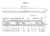
- FIG. 3 is a cross-sectional view of the liquid crystal display shown in FIG. 2 taken along line III-III.
- FIG. 4 is a layout view of the liquid crystal display shown in FIG. 2 without the pixel electrode.
- FIG. 5 is a top plan view showing the pixel electrode of the liquid crystal display show in FIG. 2 .
- FIG. 6 is a top plan view of a basic electrode of the pixel electrode according to an exemplary embodiment of the present invention.
- FIG. 7 is an enlarged view of the portion of the basic electrode shown in FIG. 6 .
- FIG. 8 is a view showing a process of pretilting liquid crystal molecules using prepolymers polarized by light such as ultraviolet rays.
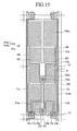
- FIG. 9 , FIG. 12 , and FIG. 15 are layout views of a liquid crystal display according to another exemplary embodiment of the present invention.
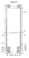
- FIG. 10 , FIG. 13 , and FIG. 16 are layout views of the liquid crystal displays shown in FIG. 9 , FIG. 12 , and FIG. 15 without the pixel electrodes.
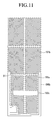
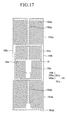
- FIG. 11 , FIG. 14 , and FIG. 17 are top plan views of the pixel electrodes in the liquid crystal displays shown in FIG. 9 , FIG. 12 , and FIG. 15 .
- FIG. 18 is a top plan view of a portion of a pixel electrode in a liquid crystal display according to another exemplary embodiment of the present invention.
- FIG. 19 is a top plan view of the portion of the pixel electrode shown in FIG. 18 .
- FIG. 1 is an equivalent circuit diagram of one pixel in a liquid crystal display according to an exemplary embodiment of the present invention.
- a liquid crystal display includes signal lines, which include a plurality of gate lines GL, a plurality of pairs of data lines DLa and DLb, and a plurality of storage electrode lines SL, and a plurality of pixels PX connected to the signal lines.
- the liquid crystal display includes a lower panel 100 and an upper panel 200 facing each other, and a liquid crystal layer 3 disposed therebetween.
- Each pixel PX includes a pair of subpixels PXa and PXb.
- Each subpixel PXa/PXb includes a switching element Qa/Qb, a liquid crystal capacitor Clca/Clcb, and a storage capacitor Csta/Cstb.
- Each switching element Qa/Qb is a three-terminal element, such as a thin film transistor, provided on a lower panel 100 and including a control terminal connected to the gate line GL, an input terminal connected to the data line DLa/DLb, and an output terminal connected to the liquid crystal capacitor Clca/Clcb and the storage capacitor Csta/Cstb.
- the liquid crystal capacitor Clca/Clcb uses a subpixel electrode and a common electrode 270 as two terminals.
- the liquid crystal layer 3 between the electrodes 191a/191b and 270 functions as a dielectric material.
- the storage capacitor Csta/Cstb serving as an assistant to the liquid crystal capacitor Clca/Clcb includes a storage electrode line SL on the lower display panel 100, a subpixel electrode 191a/191b overlapping the storage electrode line, and an insulator disposed therebetween.
- a voltage such as a common voltage Vcom, is applied to the storage electrode line SL.
- a difference is generated between the voltages charged to two liquid crystal capacitors Clca and Clcb.
- the data voltage applied to the liquid crystal capacitor Clca may less than or greater than the data voltage applied to the liquid crystal capacitor Clcb. Therefore, when the voltages of the first and second liquid crystal capacitors Clca and Clcb are appropriately adjusted, it may be possible to make an image viewed from the side as similar as possible to an image viewed from the front, thereby improving the side visibility.
- FIG. 2 a liquid crystal display according to an exemplary embodiment of the present invention will be described in detail with reference to FIG. 2 , FIG. 3 , FIG. 4 , FIG. 5 , FIG. 6, and FIG. 7 .
- FIG. 2 is a layout view of a liquid crystal display according to an exemplary embodiment of the present invention
- FIG. 3 is a cross-sectional view of the liquid crystal display shown in FIG. 2 taken along line III-III
- FIG. 4 is a layout view of the liquid crystal display shown in FIG. 2 without the pixel electrode
- FIG. 5 is a top plan view showing the pixel electrode of the liquid crystal display show in FIG. 2
- FIG. 6 is a top plan view of a basic electrode of the pixel electrode according to an exemplary embodiment of the present invention
- FIG. 7 is an enlarged view of a portion of the basic electrode shown in FIG. 6 .
- a liquid crystal display according to an exemplary embodiment of the present invention includes a lower panel 100 and an upper panel 200 facing each other, and a liquid crystal layer 3 disposed between the two panels 100 and 200.
- a plurality of gate lines 121 and a plurality of storage electrode lines 131 are formed on an insulating substrate 110.
- the gate lines 121 transmit gate signals and extend in a transverse direction.
- Each gate line 121 includes a plurality of first and second gate electrodes 124a and 124b protruding upward.
- the storage electrode lines 131 include a stem extending substantially parallel to the gate lines 121, and a plurality of branches extending from the stem. Each branch includes a longitudinal portion 137, a loop 135, a first storage electrode 133a, and a second storage electrode 133b.
- the longitudinal portion 137 extends upward and downward from the stem (hereinafter, an imaginary straight line in the direction in which the longitudinal portion 137 extends is referred to as a "longitudinal center line").
- the loop 135 may be substantially rectangular, and the upper edge thereof vertically may meet the longitudinal portion 137.
- the first storage electrode 133a extends in a transverse direction from the center of the left edge of the loop 135 to the center of the right edge, and may have a wider width than the longitudinal portion 137 or the loop 135.
- the first storage electrode 133a and the longitudinal portion 137 vertically meet each other.
- the left edge of the loop 135 extends downward and curves to the right to form the second storage electrode 133b.
- the width of the second storage electrode 133b is expanded and extends substantially parallel to the first storage electrode 133a in the transverse direction.
- the shapes and arrangement of the storage electrode lines 131 may be modified in various forms.
- a gate insulating layer 140 is formed on the gate lines 121 and the storage electrode lines 131 and a plurality of semiconductors 154a and 154b, which may be made of amorphous or crystallized silicon, are formed on the gate insulating layer 140.
- a pair of ohmic contacts 163b and 165b are formed on the first semiconductor 154b, and the ohmic contacts 163b and 165b may be formed of a material such as n+ hydrogenated amorphous silicon in which an n-type impurity is doped with a high concentration or silicide.
- a pair of data lines 171a and 171b and a plurality of first and second drain electrodes 175a and 175b are formed on the ohmic contacts 163b and 165b, and on the gate insulating layer 140.
- the data lines 171a and 171b transmit data signals, extend substantially in the longitudinal direction, and cross the gate lines 121 and the storage electrode lines 131.
- Each data line 171a/171b includes a plurality of first/second source electrode 173a/173b extending toward the first/second gate electrode 124a/124b and curving with a "U" shape, and the first/ second source electrode 173a/173b is opposite the first/second drain electrode 175a/175b with respect to the first/second gate electrode 124a/124b.
- Each first drain electrode 175a has one end enclosed by the first source electrode 173a from which it extends upward, curves to the left following the upper edge of the second storage electrode 133b, and again extends upward near the longitudinal center line to form the other end.
- the other end of the first drain electrode 175a extends to where the second storage electrode 133b is disposed, and has a wide area for connection with another layer.
- Each second drain electrode 175b has one end enclosed by the second source electrode 173b from which it extends upward to the second storage electrode 133b, curves to the right, extends following the lower edge of the second storage electrode 133b, expands with a wide area near the longitudinal center line, and again extends downward to form a longitudinal portion 176.
- first and second drain electrodes 175a and 175b and the data lines 171a and 171b may be modified in various ways.
- a first/second gate electrode 124a/124b, a first/second source electrode 173a/173b, and a first/second drain electrode 175a/175b respectively form a first/second thin film transistor (TFT) Qa/Qb along with a first/second semiconductor 154a/154b, and a channel of the first /second thin film transistor Qa/Qb is formed on the first/second semiconductor 154a/154b between the first/second source electrode 173a/173b and the first/second drain electrode 175a/175b.
- TFT thin film transistor
- the ohmic contacts 163b and 165b are disposed only between the underlying semiconductor islands 154a and 154b and the overlying data lines 171 a and 171b and drain electrodes 175a and 175b, and may reduce contact resistance between them.
- the semiconductors 154a and 154b each have a portion that is exposed without being covered by the data lines 171a and 171b and the drain electrodes 175a and 175b, and a portion between the source electrodes 173a and 173b and the drain electrodes 175a and 175b.
- a lower passivation layer 180p which may be made of silicon nitride or silicon oxide, is formed on the data lines 171a and 171b, the drain electrodes 175a and 175b, and the exposed portions of the semiconductors 154a and 154b.
- a black matrix including a plurality of light blocking members 220 spaced at intervals from each other is formed on the lower passivation layer 180p.
- Each light blocking member 220 may include a stripe portion extending upward and downward, and a quadrangle portion corresponding to the thin film transistor to prevent light leakage.
- a plurality of color filters 230 are formed on the lower passivation layer 180p and the light blocking members 220.
- the color filters 230 are mostly formed in a region surrounded by light blocking members 220.
- the color filters 230 have a plurality of holes 235a and 235b disposed on the first and second drain electrodes 175a and 175b, and a plurality of openings 233a and 233b disposed on the first and second storage electrodes 133a and 133b, respectively.
- the opening 233a and 233b reduce the thickness of the dielectric material forming the storage capacitors Csta and Cstb such that the storage capacitance may be increased.
- the lower passivation layer 180p may prevent pigments of the color filter 230 from flowing into the exposed semiconductors 154a and 154b.
- the upper passivation layer 180q is formed on the light blocking members 220 and the color filters 230.
- the upper passivation layer 180q may be made of an inorganic insulating material, such as silicon nitride or silicon oxide, and may prevent the color filters 230 from lifting and suppress the contamination of the liquid crystal layer 3 by the organic material, such as a solvent flowing from the color filters 230, so defects generated during driving, such as an afterimage, may be prevented.
- At least one of the light blocking members 220 and the color filters 230 may be disposed on the upper panel 200, and one of the lower passivation layer 180p and the upper passivation layer 180q of the lower panel 100 may be omitted in this case.
- the upper passivation layer 180q and the lower passivation layer 180p have a plurality of contact holes 185a and 185b respectively exposing the first and second drain electrodes 175a and 175b.
- a plurality of pixel electrodes 191 is formed on the upper passivation layer 180q, and the above-described color filters 230 may extend according to a column of the pixel electrodes 191.
- each pixel electrode 191 includes the first and second subpixel electrodes 191a and 191b that are spaced apart from each other with a gap 91 having a quadrangular belt shape therebetween, and the first and second subpixel electrodes 191a and 191 b respectively include a basic electrode 199 shown in FIG. 6 , or at least one modification thereof.
- the basic electrode 199 may be a quadrangle and may include a cross-shaped stem having a transverse stem 193 that crosses a longitudinal stem 192. Also, the basic electrode 199 is divided into a first subregion Da, a second subregion Db, a third subregion Dc, and a fourth subregion Dd by the transverse stem 193 and the longitudinal stem 192, and each subregion Da-Dd includes a plurality of first, second, third, and fourth branches 194a, 194b, 194c, and 194d.
- the first branch 194a extends obliquely from the transverse stem 193 or the longitudinal stem 192 in the upper-left direction, as shown in FIG. 7
- the second branch 194b extends obliquely from the transverse stem 193 or the longitudinal stem 192 in the upper-right direction
- the third branch 194c extends obliquely from the transverse stem 193 or the longitudinal stem 192 in the lower-left direction
- the fourth branch 194d extends obliquely from the transverse stem 193 or the longitudinal stem 192 in the lower-right direction.
- the first, second, third, and fourth branches 194a, 194b, 194c, and 194d form an angle of about 45 degrees or 135 degrees with the gate lines 121 or the transverse stem 193. Also, the branches 194a, 194b, 194c, and 194d of two neighboring subregions Da, Db, Dc, and Dd may be crossed.
- the width of the branches 194a, 194b, 194c, and 194d may be in the range of 2.5 ⁇ m to 5.0 ⁇ m, and the interval between the neighboring branches 194a, 194b, 194c, and 194d in one subregion Da, Db, Dc, and Dd may be in the range of 2.5 ⁇ m to 5.0 ⁇ m.
- the width of the branches 194a, 194b, 194c, and 194d may become wider approaching the transverse stem 193 or the longitudinal stem 192, and the difference between the widest width and the narrowest width in one of the branches 194a, 194b, 194c, and 194d may be in the range of 0.2 ⁇ m to 1.5 ⁇ m.
- the first subpixel electrode 191a includes one basic electrode 199 as shown in FIG. 6 .
- the transverse stem 193 of the basic electrode 199 forming the first subpixel electrode 191a expands downward and upward to form a first expansion 193a, and the first expansion 193a overlaps the first storage electrode 133a.
- the protrusion that protrudes downward to contact the first drain electrode 175a is formed in the center of the downward edge of the first expansion 193a.
- the second subpixel electrode 191 b includes an upper electrode 191 bu and a lower electrode 191 bb, and each of the upper electrode 191 bu and the lower electrode 191 bb includes one basic electrode 199.
- the upper electrode 191 bu and the lower electrode 191 bb are connected to each other through left and right connections 195b.
- the second subpixel electrode 191b encloses the first subpixel electrode 191a with the gap 91 therebetween.
- a portion of the center of the transverse stem of the lower electrode 191bb extends upward and downward to form a second expansion 193bb overlapping the second storage electrode 133b.
- the protrusion that protrudes downward to contact the second drain electrode 175b is formed in the center of the downward edge of the second expansion 193bb.
- the area of the second subpixel electrode 191 b may be about 1.0 to 2.2 times the area of the first subpixel electrode 191a.
- Each first/second subpixel electrode 191a/191b is connected to the first/second drain electrode 175a/175b through the contact hole 185a/185b, and receives data voltages from the first/second drain electrode 175a/175b.
- the upper electrode 191 bu may receive the data voltages directly from the second drain electrode 175b.
- the second drain electrode 175b extends to the upper electrode 191bu, and a contact hole (not shown) through which the upper electrode 191 bu contacts the second drain electrode 175b is required.
- the left and right connections 195b are not necessary.
- An alignment layer 11 is formed on the pixel electrodes 191.
- a common electrode 270 is formed on an insulating substrate 210, and an alignment layer 21 is formed thereon.
- Each alignment layer 11 and 21 may be a vertical alignment layer.
- polarizers may be provided on the outer surface of the display panels 100 and 200.
- the liquid crystal layer 3 disposed between the lower panel 100 and the upper panel 200 includes liquid crystal molecules 310 and polymers 350 and 370 having negative dielectric anisotropy.
- the liquid crystal molecules 310 are pretilted by the polymers 350 and 370 for the long axis thereof to be parallel to the directions in which the first, second, third, and fourth branches 194a, 194b, 194c, and 194d of the first and second subpixel electrode 191 a and 191 b extend, and are aligned vertically with respect to the surface of the two panels 100 and 200. Accordingly, the first and second subpixels PXa and PXb each include four subregions Da, Db, Dc, and Dd in which the liquid crystal molecules 310 are pretilted in different directions.
- the data voltage is applied to the first and second subpixel electrodes 191a and 191b through the data lines 171a and 171b. Then, the first and second subpixel electrodes 191a and 191 b receive the data voltage and the common electrode 270 receives the common voltage, thereby generating an electric field in the liquid crystal layer 3. Accordingly, the liquid crystal molecules 310 of the liquid crystal layer 3 are arranged in response to the electric field such that the major axes of the liquid crystal molecules 310 change direction to be perpendicular to the direction of the electric field.
- the degree to which the polarization of light incident to the liquid crystal layer 3 changes depends on the inclination degree of the liquid crystal molecules 310, and the change in the polarization is represented by a change in the transmittance by a polarizer, thereby causing the liquid crystal display to display an image.
- the edges of the branches 194a, 194b, 194c, and 194d distort the electric field to make the horizontal components perpendicular to the edges of the branches 194a, 194b, 194c, and 194d, and the alignment of the liquid crystal molecules 310 is determined by the horizontal components. Accordingly, the liquid crystal molecules 310 first tend to tilt in a direction perpendicular to the edges of the branches 194a, 194b, 194c, and 194d.
- the directions of the horizontal components of the electric field by the neighboring branches 194a, 194b, 194c, and 194d are opposite to each other and the intervals between the branches 194a, 194b, 194c, and 194d are narrow such that the liquid crystal molecules 310, which tend to arrange in opposite directions, are tilted in the direction parallel to the directions in which the branches 194a, 194b, 194c, and 194d extend.
- the liquid crystal molecules 310 may be tilted in the directions in which the branches 194a, 194b, 194c, and 194d extend through two steps.
- the liquid crystal molecules 310 are already pretilted in a direction parallel to the directions of in which branches 194a, 194b, 194c, and 194d extend so the liquid crystal molecules 310 are pretilted in one step. Therefore, if the liquid crystal molecules 310 are pretilted, they may be tilted in the required direction in one step such that the response speed of the liquid crystal display may be improved.
- the branches 194a, 194b, 194c, and 194d extend in different directions in one pixel PX such that the the liquid crystal molecules 310 are inclined in four directions. Therefore, the viewing angle of the liquid crystal display may be widened by varying the inclined directions of the liquid crystal molecules.
- the first/second sub-pixel electrode 191a/191b and the common electrode 270 form the liquid crystal capacitor Clca/Clcb to maintain an applied voltage even after the TFT is turned off. Also, the first and second storage electrodes 133a and 133b of the storage electrode line 131 respectively overlap the first and second subpixel electrodes 191a and 191b in the openings 188a and 188b to form the storage capacitors Csta and Cstb.
- the loop 135 of the storage electrode line 131 overlaps the gap 91 of the pixel electrode 191 such that it functions as a shielding member to block light leakage between the first subpixel electrode 191a and the second subpixel electrode 191b.
- the loop 135 disposed between the data lines 171a and 171 b, and the first subpixel electrode 191a, may prevent crosstalk, which may reduce degradation of the display quality.
- the alignment of the liquid crystal molecules 310 may not be controlled near the longitudinal and the transverse stems of the first and second subpixel electrodes 191a and 191b so texture may be generated. Accordingly, the storage electrode line 131, the longitudinal portion 137 of the storage electrode line 131, and the first and second storage electrodes 133a and 133b overlap the transverse stem or the longitudinal stem of the first and second subpixel electrodes 191a and 191 b such that the texture may be covered, so the aperture ratio may be increased.
- the first subpixel electrode 191a and the second subpixel electrode 191 b are applied with different data voltages through the different data lines 171a and 171b, and the voltage of the first subpixel electrode 191a having a relatively small area is higher than the voltage of the second subpixel electrode 191 b having a relatively large area.
- the voltage applied to the first liquid crystal capacitor Clca formed between the first sub-pixel electrode 191a and the common electrode 270 and the voltage applied to the second liquid crystal capacitor Clcb formed between the second sub-pixel electrode 191b and the common electrode 270 are different from each other such that the declination angle of the liquid crystal molecules of the subpixels PXa and PXb are different from each other, and as a result the luminance of the two subpixels become different.
- the images shown at the side may be approximate to the image shown at the front, that is to say, the gamma curve of the side may be approximately close to the gamma curve of the front, which may improve the side visibility.
- the first subpixel electrode 191a applied with the higher voltage is disposed in the center of the pixel PX, the first subpixel electrode 191a is father apart from the gate line 121 such that an overlapping portion therebetween is not generated, which may reduce a kick-back voltage and remove flicker.
- FIG. 8 is a view showing a process for pretilting liquid crystal molecules using prepolymers, which are polymerized by light such as ultraviolet rays.
- prepolymers 330 such monomers, which are hardened through polymerization by light such as ultraviolet rays, are inserted between the two display panels 100 and 200 along with the liquid crystal material.
- the prepolymers 330 may include reactive mesogen that is polymerized by light, such as ultraviolet rays.
- the first and second subpixel electrodes 191a and 191b receive the data voltages and the common electrode 270 of the upper panel 200 receives the common voltage to generate an electric field to the liquid crystal layer 3 between two display panels 100 and 200.
- the liquid crystal molecules 310 of the liquid crystal layer 3 are inclined in a direction parallel to the length direction of the branches 194a, 194b, 194c, and 194d through two steps, as above-described, in response to the electric field, and the liquid crystal molecules 310 in one pixel PX are inclined in a total of four directions.
- the prepolymers 330 are polymerized such that the first polymer 350 and the second polymer 370 are formed as shown in FIG. 8 .
- the first polymer 350 is formed in the liquid crystal layer 3, and the second polymer 370 is formed close to the display panels 100 and 200.
- the liquid crystal molecules 310 are pretilted in the directions in which the branches 194a, 194b, 194c, and 194d extend by the first and second polymers 350 and 370.
- liquid crystal molecules 310 are arranged to pretilt in four different directions when no voltage is applied to the electrodes 191 and 270.
- FIG. 9 Another exemplary embodiment of the present invention will be described with the reference to FIG. 9 , FIG. 10 , and FIG. 11 .
- FIG. 9 is a layout view of a liquid crystal display according to another exemplary embodiment of the present invention
- FIG. 10 is a layout view of the liquid crystal display shown in FIG. 9 without the pixel electrode
- FIG. 11 is a top plan view showing the pixel electrode of the liquid crystal display shown in FIG. 9 .
- the layered structure of the liquid crystal display according to the present exemplary embodiment is almost the same as the layered structure of the liquid crystal display shown in FIG. 2 , FIG. 3 , FIG. 4 , and FIG. 5 .
- the storage electrode line 131 includes left and right longitudinal portions 138 extending downward from the storage electrode line 131, and a storage electrode 133 protruding in the right direction from the left longitudinal portion 138.
- the storage electrode 133 has the wider width than that of the other portion for overlapping with a pixel electrode 191 to be described below.
- the first drain electrode 175a includes one end having a wide area extending a long distance upward
- the second drain electrode 175b includes one end having a wide area extending a short distance upward.
- the color filters (not shown) have through holes 235a and 235b where contact holes 185a and 185b pass through and an opening 233 disposed on the storage electrode 133, and an upper passivation layer (not shown) and a lower passivation layer (not shown) have a plurality of contact holes 185a and 185b to expose the first and second drain electrodes 175a and 175b.
- the pixel electrode 191 also includes first and second subpixel electrodes 191a and 191b that are spaced apart from each other with a gap 91 having a quadrangular belt shape, like the exemplary embodiment shown in FIG. 2 , FIG. 3 , FIG. 4 , and FIG. 5 .
- the first subpixel electrode 191a is made of one basic electrode 199, as shown in FIG. 6 .
- a transverse stem of the first subpixel electrode 191 a expands upward and downward to form an expansion 193c, and the expansion 193c overlaps the storage electrode 133 in an opening 233 to form a storage capacitor Csta.
- the second subpixel electrode 191 b includes one basic electrode 199, and a connection bridge 196b enclosing the first subpixel electrode 191 a, which is disposed below the second subpixel electrode 191b with a gap 91 therebetween.
- connection bridge 196b protrudes to the right with a wide area to contact the second drain electrode 175b.
- the second subpixel electrode 191b receives data voltages from the second drain electrode 175b through the connection bridge 196b.
- connection bridge 196b overlaps a portion of the gate line 121 to prevent the first subpixel electrode 191 a from being influenced by the gate signals of the gate lines 121.
- connection bridge 196b cover the data lines 171 a and 171 b to prevent cross talk between the data signal and the first subpixel electrode 191a.
- connection bridge 196b may be in the range of 5.0 ⁇ m to 15 ⁇ m.
- the storage electrode line 131 overlaps the gap 91 of the pixel electrode 191 to block light leakage between the first subpixel electrode 191a and the second subpixel electrode 191b. Also, the right and left longitudinal portions 138 of the storage electrode line 131 are disposed between the first subpixel electrode 191a and the data lines 171a and 171b, to prevent cross talk between the data lines 171a and 171b and the first subpixel electrode 191a.
- the area of the second subpixel electrode 191b may be about 1.25 to 2.75 times the area of the first subpixel electrode 191 a.
- the first/second drain electrode 175a/175b do not overlap the second/first subpixel electrode 191 b/191 a that receive data voltages having different polarities from each other, but instead overlap only the first/second subpixel electrode 191a/191b that receive data voltages having the same polarity such that a texture due to distortion of the electric field is not generated near the first and second drain electrodes 175a and 175b even though the first and second data lines 171a and 171b receive data voltages of opposite polarities. Accordingly, texture may be prevented, which may increase transmittance.
- the contact holes 185a and 185b are disposed at edges or corners of the first and second subpixel electrodes 191a and 191b so that it may be easy to form color filters (not shown) by an inkjet printing process.
- the liquid crystal molecules are inclined in four directions such that the viewing angle of the liquid crystal display may be increased, and the liquid crystal molecules are pretilted through the polymerization of the prepolymer such that the response speed may be improved.
- the first and second subpixel electrodes 191a and 191 b receive different data voltages, which may improve side visibility.
- FIG. 12 Next, another exemplary embodiment of the present invention will be described with reference to FIG. 12 , FIG. 13 , and FIG. 14 .
- FIG. 12 is a layout view of a liquid crystal display according to another exemplary embodiment of the present invention
- FIG. 13 is a layout view of the liquid crystal display shown in FIG. 12 without the pixel electrode
- FIG. 14 is a top plan view showing the pixel electrode of the liquid crystal display shown in FIG. 12 .
- a liquid crystal display according to the present exemplary embodiment is almost the same as the liquid crystal display shown in FIG. 9 , FIG. 10 , and FIG. 11 .
- the wide end portion of the first drain electrode 175a to apply the data voltage to the first subpixel electrode 191 a is disposed at the right lower corner of the first subpixel PXa, and is connected to the first subpixel electrode 191a through the contact hole 185a. Accordingly, when forming the color filter (not shown) through an inkjet printing process, the process may be easily executed and the transmittance may be improved.
- the storage electrodes and the openings having a wide area to form the storage capacitors Csta and Cstb do not exist in the present exemplary embodiment, which may increase the aperture ratio.
- FIG. 15 Next, another exemplary embodiment of the present invention will be described with reference to FIG. 15 , FIG. 16 , and FIG. 17 .
- FIG. 15 is a layout view of a liquid crystal display according to another exemplary embodiment of the present invention
- FIG. 16 is a layout view of the liquid crystal display shown in FIG. 15 except for the pixel electrode
- FIG. 17 is a top plan view showing the pixel electrode of the liquid crystal display shown in FIG. 15 .
- the layered structure of the liquid crystal display according to the present exemplary embodiment is almost the same as the layered structure of the liquid crystal display shown in FIG. 2 , FIG. 3 , FIG. 4 , and FIG. 5 .
- the storage electrode line 131 includes left and right longitudinal portions 139 that extend upward and downward from the storage electrode line 131, a transverse connection 132 connected between two longitudinal portions 139, and a storage electrode 133c protruding from the center of the transverse connection 132 to the lower direction and having a wide area.
- the color filters (not shown) have through holes 235a and 235b where contact holes 185a and 185b pass through, and an opening 233 disposed on the storage electrode 133c, and an upper passivation layer (not shown) and a lower passivation layer (not shown) have a plurality of contact holes 185a and 185b exposing the first and second drain electrodes 175a and 175b.
- the pixel electrode 191 also includes the first and second subpixel electrodes 191 a and 191 b that are spaced apart from each other with a gap 91 having a quadrangular belt shape.
- the second subpixel electrode 191 b includes an upper electrode 191 bu and a lower electrode 191 bb, and the upper electrode 191 bu and the lower electrode 191 bb are connected through left and right connections 195b.
- Two longitudinal portions 139 of the storage electrode line 131 overlap the gap 91 to block light leakage between the first subpixel electrode 191a and the second subpixel electrode 191b and prevent cross talk between the first subpixel electrode 191 a and the data lines 171a and 171b. Also, the transverse connection 132 of the storage electrode line 131 covers the texture near the transverse stem 193d of the first subpixel electrode 191 a, which may improve the aperture ratio.
- a transverse stem 193du of the upper electrode 191 bu is not disposed on the center of the upper electrode 191 bu, but is near the upper edge, and the transverse stem 193db of the lower electrode 191 bb is disposed near the lower edge of the lower electrode 191 bb. Accordingly, as for each of the upper and lower electrodes 191bu and 191 bb, two subregions among four subregions Da, Db, Dc, and Dd of the basic electrode 199 of FIG. 6 as above-described almost disappear and remain as dummies. However, all of the subregions Da, Db, Dc, and Dd still exist in the second subpixel electrode 191b such that the liquid crystal molecules 310 may be inclined in four directions.
- the area of the two remaining subregions Dc and Dd of the upper electrode 191 bu may be more than 1.5 times the area of the two subregions Da and Db, which become small.
- the area of the two remaining subregions Da and Db of the lower electrode 191 bb may be more than 1.5 times the area of the two subregions Dc and Dd, which may become small.
- the length between the upper edge and the lower edge of the two subregions Da and Db of the upper electrode 191 bu or two subregions Dc and Dd of the lower electrode 191 bb, which may become small, may be about 5 ⁇ m.
- FIG. 18 is a top plan view of a portion of a pixel electrode in a liquid crystal display according to another exemplary embodiment of the present invention
- FIG. 19 is a top plan view of the portion of the pixel electrode shown in FIG. 17 .
- the liquid crystal molecules 310 are inclined in the direction D1 such that the horizontal inclination direction of the liquid crystal molecules 310 of the subregions Da and Db is the same as that of the liquid srystal molecules 310 of the subregions Dc and Dd, and thereby the texture may be weakened.
- the longitudinal stems 192du and 192db of the upper and the lower electrodes 191 bu and 191 bb of the second subpixel electrode 191 b may be positioned near the left edge or the right edge of the pixel PX, instead of locating the transverse stems 193du and 193db of the upper or lower electrodes 191bu or 191bb of the second subpixel electrode 191b near the upper and lower edges of the pixel PX like the present exemplary embodiment, such that a difference between the areas of the left subregions Da and Dc and the right subregions Db and Dd may be generated.
- the area of the subregions which become wide may be more than 1.5 times the area of the subregions which become small.
- the transverse stem 193 of the first subpixel electrode 191a does not include the expanded portion, and the portion disposed under the longitudinal stem 192 expands at both sides to form a third expansion 192a. Also, the a portion to contact with the first drain electrode 175a is formed under the third expansion 192a, and another wide portion for the contact with the second drain electrode 175b is formed at the bottom of the longitudinal stem 192db of the lower electrode 191 bb of the second subpixel electrode 191b.
- the liquid crystal molecules are inclined in four directions so that the viewing angle of the liquid crystal display may be increased, and the liquid crystal molecules are pretilted by the polymerization of the prepolymer, which may improve the response speed.
- the first and second subpixel electrodes 191a and 191b receive different data voltages, which may improve side visibility.
- a light alignment method in which light such as ultraviolet rays is obliquely irradiated to the alignment layers 11 and 21 may be used to control the alignment direction and the alignment angle of the liquid crystal molecules 310 to form a plurality of subregions Da, Db, Dc, and Dd where the liquid crystal molecules 310 are inclined in different directions.
- the branches 194a, 194b, 194c, and 194d of the pixel electrodes 191 are not necessary to increase the aperture ratio and improve the response time due to the pretilt of the liquid crystal molecules 310, which is generated by light alignment.
Landscapes
- Physics & Mathematics (AREA)
- Nonlinear Science (AREA)
- Mathematical Physics (AREA)
- Chemical & Material Sciences (AREA)
- Crystallography & Structural Chemistry (AREA)
- General Physics & Mathematics (AREA)
- Optics & Photonics (AREA)
- Engineering & Computer Science (AREA)
- Microelectronics & Electronic Packaging (AREA)
- Spectroscopy & Molecular Physics (AREA)
- Geometry (AREA)
- Liquid Crystal (AREA)
Abstract
Description
- This application claims priority from and the benefit of Korean Patent Application No.
10-2008-0029090, filed on March 28, 2008 - FIELD OF THE INVENTION
- The present invention relates to a liquid crystal display.
- DISCUSSION OF THE BACKGROUND
- Liquid crystal displays (LCDs) are one of the most widely used flat panel displays, and an LCD includes a pair of panels provided with field-generating electrodes, such as pixel electrodes and a common electrode, and a liquid crystal (LC) layer disposed between the two panels. The LCD displays images when voltages are applied to the field-generating electrodes to generate an electric field in the LC layer, which determines the orientations of LC molecules therein, thereby adjusting the polarization of light incident thereto.
- Among LCDs, a vertical alignment (VA) mode LCD, in which LC molecules are aligned such that the long axes of the LC molecules are perpendicular to the panels in the absence of an electric field, has been developed.
- In a VA mode LCD, a wide viewing angle can be realized due to cutouts, such as slits in the field-generating electrodes and protrusions on the field-generating electrodes. Since the cutouts and protrusions may determine the tilt directions of the LC molecules, the tilt directions may be distributed in several directions using the cutouts and protrusions, thereby widening the reference viewing angle.
- Also, a method for pretilting LC molecules in the absence of an electric field has been developed to improve the response speed of the LC molecules while realizing a wide viewing angle. For the LC molecules to pretilt in various directions, alignment layers having various alignment directions may be used. Alternatively, the LC layer may be subjected to an electric field and a thermal or light-hardened material may be added. Then light may be irradiated onto the LC layer to harden the thermal or light-hardening material, thereby pretilting the LC molecules.
- However, the VA mode liquid crystal display may have lower side visibility compared with front visibility. To improve the side visibility, one pixel may be divided into two subpixels and different voltages may be applied to the subpixels.
- The present invention provides a liquid crystal display that may have a wide viewing angle and a fast response speed, as well as excellent visibility and transmittance.
- Additional features of the invention will be set forth in the description which follows, and in part will be apparent from the description, or may be learned by practice of the invention.
- The present invention discloses a liquid crystal display including a pixel electrode including a first subpixel electrode and a second subpixel electrode spaced apart from each other with a gap therebetween, a common electrode facing the pixel electrode, and a liquid crystal layer disposed between the pixel electrode and the common electrode. The liquid crystal layer includes a plurality of liquid crystal molecules, and the first and second subpixel electrodes include a plurality of branches. Each of the first and second subpixel electrodes includes a plurality of subregions, and the branches extend in different directions in different subregions.
- The present invention also discloses a liquid crystal display including a pixel electrode including a first subpixel electrode and a second subpixel electrode spaced apart from each other with a gap therebetween, a common electrode facing the pixel electrode, and a liquid crystal layer disposed between the pixel electrode and the common electrode and including a plurality of liquid crystal molecules. The liquid crystal layer includes a first portion disposed between the first subpixel electrode and the common electrode and a second portion disposed between the second subpixel electrode and the common electrode. Each of the first and second portions includes a plurality of subregions, and the liquid crystal molecules are aligned in different directions in different subregions. Areas of the subregions are different from each other in the first portion or in the second portion.
- The present invention also discloses a liquid crystal display including a first signal line and a second signal line, a third signal line and a fourth signal line crossing the first and second signal lines, a pixel electrode including a first subpixel electrode and a second subpixel electrode spaced apart with a gap therebetween, a first switching element connected to the first signal line and the third signal line to transmit a data voltage from the third signal line to the first subpixel electrode, a second switching element connected to the first signal line and the fourth signal line to transmit a data voltage from the fourth signal line to the second subpixel electrode, a common electrode facing the pixel electrode, and a liquid crystal layer disposed between the pixel electrode and the common electrode and including a plurality of liquid crystal molecules. One of the first subpixel electrode and the second subpixel electrode includes a plurality of branches, and the one of the first subpixel electrode and the second subpixel electrode includes a plurality of subregions. The branches extend in different directions in different subregions.
- It is to be understood that both the foregoing general description and the following detailed description are exemplary and explanatory and are intended to provide further explanation of the invention as claimed.
- The accompanying drawings, which are included to provide a further understanding of the invention and are incorporated in and constitute a part of this specification, illustrate embodiments of the invention, and together with the description serve to explain the principles of the invention.
-
FIG. 1 is an equivalent circuit diagram of one pixel in a liquid crystal display according to an exemplary embodiment of the present invention. -
FIG. 2 is a layout view of a liquid crystal display according to an exemplary embodiment of the present invention. -
FIG. 3 is a cross-sectional view of the liquid crystal display shown inFIG. 2 taken along line III-III. -
FIG. 4 is a layout view of the liquid crystal display shown inFIG. 2 without the pixel electrode. -
FIG. 5 is a top plan view showing the pixel electrode of the liquid crystal display show inFIG. 2 . -
FIG. 6 is a top plan view of a basic electrode of the pixel electrode according to an exemplary embodiment of the present invention. -
FIG. 7 is an enlarged view of the portion of the basic electrode shown inFIG. 6 . -
FIG. 8 is a view showing a process of pretilting liquid crystal molecules using prepolymers polarized by light such as ultraviolet rays. -
FIG. 9 ,FIG. 12 , andFIG. 15 are layout views of a liquid crystal display according to another exemplary embodiment of the present invention. -
FIG. 10 ,FIG. 13 , andFIG. 16 are layout views of the liquid crystal displays shown inFIG. 9 ,FIG. 12 , andFIG. 15 without the pixel electrodes. -
FIG. 11 ,FIG. 14 , andFIG. 17 are top plan views of the pixel electrodes in the liquid crystal displays shown inFIG. 9 ,FIG. 12 , andFIG. 15 . -
FIG. 18 is a top plan view of a portion of a pixel electrode in a liquid crystal display according to another exemplary embodiment of the present invention. -
FIG. 19 is a top plan view of the portion of the pixel electrode shown inFIG. 18 . - The invention is described more fully hereinafter with reference to the accompanying drawings, in which embodiments of the invention are shown. This invention may, however, be embodied in many different forms and should not be construed as limited to the embodiments set forth herein. Rather, these embodiments are provided so that this disclosure is thorough, and will fully convey the scope of the invention to those skilled in the art. In the drawings, the size and relative sizes of layers and regions may be exaggerated for clarity. Like reference numerals in the drawings denote like elements.
- It will be understood that when an element or layer is referred to as being "on" or "connected to" another element or layer, it can be directly on or directly connected to the other element or layer, or intervening elements or layers may be present. In contrast, when an element is referred to as being "directly on" or "directly connected to" another element or layer, there are no intervening elements or layers present.
-
FIG. 1 is an equivalent circuit diagram of one pixel in a liquid crystal display according to an exemplary embodiment of the present invention. - Referring to
FIG. 1 , a liquid crystal display according to an exemplary embodiment of the present invention includes signal lines, which include a plurality of gate lines GL, a plurality of pairs of data lines DLa and DLb, and a plurality of storage electrode lines SL, and a plurality of pixels PX connected to the signal lines. The liquid crystal display includes alower panel 100 and anupper panel 200 facing each other, and aliquid crystal layer 3 disposed therebetween. - Each pixel PX includes a pair of subpixels PXa and PXb. Each subpixel PXa/PXb includes a switching element Qa/Qb, a liquid crystal capacitor Clca/Clcb, and a storage capacitor Csta/Cstb.
- Each switching element Qa/Qb is a three-terminal element, such as a thin film transistor, provided on a
lower panel 100 and including a control terminal connected to the gate line GL, an input terminal connected to the data line DLa/DLb, and an output terminal connected to the liquid crystal capacitor Clca/Clcb and the storage capacitor Csta/Cstb. - The liquid crystal capacitor Clca/Clcb uses a subpixel electrode and a
common electrode 270 as two terminals. Theliquid crystal layer 3 between theelectrodes 191a/191b and 270 functions as a dielectric material. - The storage capacitor Csta/Cstb serving as an assistant to the liquid crystal capacitor Clca/Clcb includes a storage electrode line SL on the
lower display panel 100, asubpixel electrode 191a/191b overlapping the storage electrode line, and an insulator disposed therebetween. A voltage, such as a common voltage Vcom, is applied to the storage electrode line SL. - A difference is generated between the voltages charged to two liquid crystal capacitors Clca and Clcb. For example, the data voltage applied to the liquid crystal capacitor Clca may less than or greater than the data voltage applied to the liquid crystal capacitor Clcb. Therefore, when the voltages of the first and second liquid crystal capacitors Clca and Clcb are appropriately adjusted, it may be possible to make an image viewed from the side as similar as possible to an image viewed from the front, thereby improving the side visibility.
- Next, a liquid crystal display according to an exemplary embodiment of the present invention will be described in detail with reference to
FIG. 2 ,FIG. 3 ,FIG. 4 ,FIG. 5 ,FIG. 6, and FIG. 7 . -
FIG. 2 is a layout view of a liquid crystal display according to an exemplary embodiment of the present invention,FIG. 3 is a cross-sectional view of the liquid crystal display shown inFIG. 2 taken along line III-III,FIG. 4 is a layout view of the liquid crystal display shown inFIG. 2 without the pixel electrode,FIG. 5 is a top plan view showing the pixel electrode of the liquid crystal display show inFIG. 2 ,FIG. 6 is a top plan view of a basic electrode of the pixel electrode according to an exemplary embodiment of the present invention, andFIG. 7 is an enlarged view of a portion of the basic electrode shown inFIG. 6 . - Referring to
FIG. 2 andFIG. 3 , a liquid crystal display according to an exemplary embodiment of the present invention includes alower panel 100 and anupper panel 200 facing each other, and aliquid crystal layer 3 disposed between the twopanels - First, the
lower panel 100 will be described. - A plurality of
gate lines 121 and a plurality ofstorage electrode lines 131 are formed on an insulatingsubstrate 110. - The gate lines 121 transmit gate signals and extend in a transverse direction. Each
gate line 121 includes a plurality of first andsecond gate electrodes - The
storage electrode lines 131 include a stem extending substantially parallel to thegate lines 121, and a plurality of branches extending from the stem. Each branch includes alongitudinal portion 137, aloop 135, afirst storage electrode 133a, and asecond storage electrode 133b. - The
longitudinal portion 137 extends upward and downward from the stem (hereinafter, an imaginary straight line in the direction in which thelongitudinal portion 137 extends is referred to as a "longitudinal center line"). - The
loop 135 may be substantially rectangular, and the upper edge thereof vertically may meet thelongitudinal portion 137. - The
first storage electrode 133a extends in a transverse direction from the center of the left edge of theloop 135 to the center of the right edge, and may have a wider width than thelongitudinal portion 137 or theloop 135. Thefirst storage electrode 133a and thelongitudinal portion 137 vertically meet each other. - The left edge of the
loop 135 extends downward and curves to the right to form thesecond storage electrode 133b. The width of thesecond storage electrode 133b is expanded and extends substantially parallel to thefirst storage electrode 133a in the transverse direction. - However, the shapes and arrangement of the
storage electrode lines 131 may be modified in various forms. - A
gate insulating layer 140 is formed on thegate lines 121 and thestorage electrode lines 131 and a plurality ofsemiconductors gate insulating layer 140. - A pair of
ohmic contacts first semiconductor 154b, and theohmic contacts - A pair of
data lines second drain electrodes ohmic contacts gate insulating layer 140. - The
data lines gate lines 121 and the storage electrode lines 131. Eachdata line 171a/171b includes a plurality of first/second source electrode 173a/173b extending toward the first/second gate electrode 124a/124b and curving with a "U" shape, and the first/second source electrode 173a/173b is opposite the first/second drain electrode 175a/175b with respect to the first/second gate electrode 124a/124b. - Each
first drain electrode 175a has one end enclosed by thefirst source electrode 173a from which it extends upward, curves to the left following the upper edge of thesecond storage electrode 133b, and again extends upward near the longitudinal center line to form the other end. The other end of thefirst drain electrode 175a extends to where thesecond storage electrode 133b is disposed, and has a wide area for connection with another layer. - Each
second drain electrode 175b has one end enclosed by thesecond source electrode 173b from which it extends upward to thesecond storage electrode 133b, curves to the right, extends following the lower edge of thesecond storage electrode 133b, expands with a wide area near the longitudinal center line, and again extends downward to form a longitudinal portion 176. - However, the shapes and arrangement of the first and
second drain electrodes data lines - A first/
second gate electrode 124a/124b, a first/second source electrode 173a/173b, and a first/second drain electrode 175a/175b respectively form a first/second thin film transistor (TFT) Qa/Qb along with a first/second semiconductor 154a/154b, and a channel of the first /second thin film transistor Qa/Qb is formed on the first/second semiconductor 154a/154b between the first/second source electrode 173a/173b and the first/second drain electrode 175a/175b. - The
ohmic contacts underlying semiconductor islands overlying data lines drain electrodes semiconductors data lines drain electrodes source electrodes drain electrodes - A
lower passivation layer 180p, which may be made of silicon nitride or silicon oxide, is formed on thedata lines drain electrodes semiconductors - A black matrix including a plurality of light blocking
members 220 spaced at intervals from each other is formed on thelower passivation layer 180p. Eachlight blocking member 220 may include a stripe portion extending upward and downward, and a quadrangle portion corresponding to the thin film transistor to prevent light leakage. - A plurality of
color filters 230 are formed on thelower passivation layer 180p and thelight blocking members 220. The color filters 230 are mostly formed in a region surrounded by light blockingmembers 220. The color filters 230 have a plurality ofholes second drain electrodes openings second storage electrodes opening - Here, the
lower passivation layer 180p may prevent pigments of thecolor filter 230 from flowing into the exposedsemiconductors - An
upper passivation layer 180q is formed on thelight blocking members 220 and the color filters 230. Theupper passivation layer 180q may be made of an inorganic insulating material, such as silicon nitride or silicon oxide, and may prevent thecolor filters 230 from lifting and suppress the contamination of theliquid crystal layer 3 by the organic material, such as a solvent flowing from thecolor filters 230, so defects generated during driving, such as an afterimage, may be prevented. - However, at least one of the
light blocking members 220 and thecolor filters 230 may be disposed on theupper panel 200, and one of thelower passivation layer 180p and theupper passivation layer 180q of thelower panel 100 may be omitted in this case. - The
upper passivation layer 180q and thelower passivation layer 180p have a plurality ofcontact holes second drain electrodes - A plurality of
pixel electrodes 191 is formed on theupper passivation layer 180q, and the above-describedcolor filters 230 may extend according to a column of thepixel electrodes 191. - Referring to
FIG. 5 , eachpixel electrode 191 includes the first andsecond subpixel electrodes gap 91 having a quadrangular belt shape therebetween, and the first andsecond subpixel electrodes basic electrode 199 shown inFIG. 6 , or at least one modification thereof. - Next, the
basic electrode 199 will be described in detail with reference toFIG. 6 . - As shown in
FIG. 6 , thebasic electrode 199 may be a quadrangle and may include a cross-shaped stem having atransverse stem 193 that crosses alongitudinal stem 192. Also, thebasic electrode 199 is divided into a first subregion Da, a second subregion Db, a third subregion Dc, and a fourth subregion Dd by thetransverse stem 193 and thelongitudinal stem 192, and each subregion Da-Dd includes a plurality of first, second, third, andfourth branches - The
first branch 194a extends obliquely from thetransverse stem 193 or thelongitudinal stem 192 in the upper-left direction, as shown inFIG. 7 , and thesecond branch 194b extends obliquely from thetransverse stem 193 or thelongitudinal stem 192 in the upper-right direction. Also, thethird branch 194c extends obliquely from thetransverse stem 193 or thelongitudinal stem 192 in the lower-left direction, and thefourth branch 194d extends obliquely from thetransverse stem 193 or thelongitudinal stem 192 in the lower-right direction. - The first, second, third, and
fourth branches gate lines 121 or thetransverse stem 193. Also, thebranches - The width of the
branches branches - Also, referring to
FIG. 7 , the width of thebranches transverse stem 193 or thelongitudinal stem 192, and the difference between the widest width and the narrowest width in one of thebranches - Again, referring to
FIG. 2 ,FIG. 3 ,FIG. 4 , andFIG. 5 , thefirst subpixel electrode 191a includes onebasic electrode 199 as shown inFIG. 6 . Thetransverse stem 193 of thebasic electrode 199 forming thefirst subpixel electrode 191a expands downward and upward to form afirst expansion 193a, and thefirst expansion 193a overlaps thefirst storage electrode 133a. Also, the protrusion that protrudes downward to contact thefirst drain electrode 175a is formed in the center of the downward edge of thefirst expansion 193a. - The
second subpixel electrode 191 b includes anupper electrode 191 bu and alower electrode 191 bb, and each of theupper electrode 191 bu and thelower electrode 191 bb includes onebasic electrode 199. Theupper electrode 191 bu and thelower electrode 191 bb are connected to each other through left andright connections 195b. - The
second subpixel electrode 191b encloses thefirst subpixel electrode 191a with thegap 91 therebetween. A portion of the center of the transverse stem of the lower electrode 191bb extends upward and downward to form a second expansion 193bb overlapping thesecond storage electrode 133b. Also, the protrusion that protrudes downward to contact thesecond drain electrode 175b is formed in the center of the downward edge of the second expansion 193bb. - The area of the
second subpixel electrode 191 b may be about 1.0 to 2.2 times the area of thefirst subpixel electrode 191a. - Each first/
second subpixel electrode 191a/191b is connected to the first/second drain electrode 175a/175b through thecontact hole 185a/185b, and receives data voltages from the first/second drain electrode 175a/175b. - On the other hand, the
upper electrode 191 bu may receive the data voltages directly from thesecond drain electrode 175b. In this case, thesecond drain electrode 175b extends to the upper electrode 191bu, and a contact hole (not shown) through which theupper electrode 191 bu contacts thesecond drain electrode 175b is required. In this case, the left andright connections 195b are not necessary. - An
alignment layer 11 is formed on thepixel electrodes 191. - Next, the
upper panel 200 will be described. - A
common electrode 270 is formed on an insulatingsubstrate 210, and analignment layer 21 is formed thereon. - Each
alignment layer - Finally, polarizers (not shown) may be provided on the outer surface of the
display panels - The
liquid crystal layer 3 disposed between thelower panel 100 and theupper panel 200 includesliquid crystal molecules 310 andpolymers - The
liquid crystal molecules 310 are pretilted by thepolymers fourth branches second subpixel electrode panels liquid crystal molecules 310 are pretilted in different directions. - If the
gate lines 121 are applied with the gate signals, the data voltage is applied to the first andsecond subpixel electrodes data lines second subpixel electrodes common electrode 270 receives the common voltage, thereby generating an electric field in theliquid crystal layer 3. Accordingly, theliquid crystal molecules 310 of theliquid crystal layer 3 are arranged in response to the electric field such that the major axes of theliquid crystal molecules 310 change direction to be perpendicular to the direction of the electric field. The degree to which the polarization of light incident to theliquid crystal layer 3 changes depends on the inclination degree of theliquid crystal molecules 310, and the change in the polarization is represented by a change in the transmittance by a polarizer, thereby causing the liquid crystal display to display an image. - On the other hand, the edges of the
branches branches liquid crystal molecules 310 is determined by the horizontal components. Accordingly, theliquid crystal molecules 310 first tend to tilt in a direction perpendicular to the edges of thebranches branches branches liquid crystal molecules 310, which tend to arrange in opposite directions, are tilted in the direction parallel to the directions in which thebranches liquid crystal molecules 310 are not initially pretilted in the direction in which thebranches liquid crystal molecules 310 may be tilted in the directions in which thebranches liquid crystal molecules 310 are already pretilted in a direction parallel to the directions of in whichbranches liquid crystal molecules 310 are pretilted in one step. Therefore, if theliquid crystal molecules 310 are pretilted, they may be tilted in the required direction in one step such that the response speed of the liquid crystal display may be improved. - Also, in an exemplary embodiment of the present invention, the
branches liquid crystal molecules 310 are inclined in four directions. Therefore, the viewing angle of the liquid crystal display may be widened by varying the inclined directions of the liquid crystal molecules. - The first/
second sub-pixel electrode 191a/191b and thecommon electrode 270 form the liquid crystal capacitor Clca/Clcb to maintain an applied voltage even after the TFT is turned off. Also, the first andsecond storage electrodes storage electrode line 131 respectively overlap the first andsecond subpixel electrodes - The
loop 135 of thestorage electrode line 131 overlaps thegap 91 of thepixel electrode 191 such that it functions as a shielding member to block light leakage between thefirst subpixel electrode 191a and thesecond subpixel electrode 191b. Theloop 135 disposed between thedata lines first subpixel electrode 191a, may prevent crosstalk, which may reduce degradation of the display quality. - Also, in the structure of
pixel electrode 191 in an exemplary embodiment of the present invention, the alignment of theliquid crystal molecules 310 may not be controlled near the longitudinal and the transverse stems of the first andsecond subpixel electrodes storage electrode line 131, thelongitudinal portion 137 of thestorage electrode line 131, and the first andsecond storage electrodes second subpixel electrodes - On the other hand, the
first subpixel electrode 191a and thesecond subpixel electrode 191 b are applied with different data voltages through thedifferent data lines first subpixel electrode 191a having a relatively small area is higher than the voltage of thesecond subpixel electrode 191 b having a relatively large area. - In this way, if the voltages of the first
sub-pixel electrode 191 a and the secondsub-pixel electrode 191b are different from each other, the voltage applied to the first liquid crystal capacitor Clca formed between thefirst sub-pixel electrode 191a and thecommon electrode 270 and the voltage applied to the second liquid crystal capacitor Clcb formed between the secondsub-pixel electrode 191b and thecommon electrode 270 are different from each other such that the declination angle of the liquid crystal molecules of the subpixels PXa and PXb are different from each other, and as a result the luminance of the two subpixels become different. Accordingly, if the voltages of the first and second liquid crystal capacitors Clca and Clcb are appropriately controlled, the images shown at the side may be approximate to the image shown at the front, that is to say, the gamma curve of the side may be approximately close to the gamma curve of the front, which may improve the side visibility. - Also, in an exemplary embodiment of the present invention, if the
first subpixel electrode 191a applied with the higher voltage is disposed in the center of the pixel PX, thefirst subpixel electrode 191a is father apart from thegate line 121 such that an overlapping portion therebetween is not generated, which may reduce a kick-back voltage and remove flicker. - Next, the alignment method for initially pretilting
liquid crystal molecules 310 will be described with reference toFIG. 8 . -
FIG. 8 is a view showing a process for pretilting liquid crystal molecules using prepolymers, which are polymerized by light such as ultraviolet rays. - First,
prepolymers 330, such monomers, which are hardened through polymerization by light such as ultraviolet rays, are inserted between the twodisplay panels prepolymers 330 may include reactive mesogen that is polymerized by light, such as ultraviolet rays. - Next, the first and
second subpixel electrodes common electrode 270 of theupper panel 200 receives the common voltage to generate an electric field to theliquid crystal layer 3 between twodisplay panels liquid crystal molecules 310 of theliquid crystal layer 3 are inclined in a direction parallel to the length direction of thebranches liquid crystal molecules 310 in one pixel PX are inclined in a total of four directions. - If the
liquid crystal layer 3 is irradiated, for example, with ultraviolet rays, after the application of the electric field to theliquid crystal layer 3, theprepolymers 330 are polymerized such that thefirst polymer 350 and thesecond polymer 370 are formed as shown inFIG. 8 . - The
first polymer 350 is formed in theliquid crystal layer 3, and thesecond polymer 370 is formed close to thedisplay panels liquid crystal molecules 310 are pretilted in the directions in which thebranches second polymers - Accordingly, the
liquid crystal molecules 310 are arranged to pretilt in four different directions when no voltage is applied to theelectrodes - Next, another exemplary embodiment of the present invention will be described with the reference to
FIG. 9 ,FIG. 10 , andFIG. 11 . -
FIG. 9 is a layout view of a liquid crystal display according to another exemplary embodiment of the present invention,FIG. 10 is a layout view of the liquid crystal display shown inFIG. 9 without the pixel electrode, andFIG. 11 is a top plan view showing the pixel electrode of the liquid crystal display shown inFIG. 9 . - The layered structure of the liquid crystal display according to the present exemplary embodiment is almost the same as the layered structure of the liquid crystal display shown in
FIG. 2 ,FIG. 3 ,FIG. 4 , andFIG. 5 . - Referring to
FIG. 9 ,FIG. 10 , andFIG. 11 , thestorage electrode line 131 includes left and rightlongitudinal portions 138 extending downward from thestorage electrode line 131, and astorage electrode 133 protruding in the right direction from the leftlongitudinal portion 138. Thestorage electrode 133 has the wider width than that of the other portion for overlapping with apixel electrode 191 to be described below. - The
first drain electrode 175a includes one end having a wide area extending a long distance upward, and thesecond drain electrode 175b includes one end having a wide area extending a short distance upward. - The color filters (not shown) have through
holes opening 233 disposed on thestorage electrode 133, and an upper passivation layer (not shown) and a lower passivation layer (not shown) have a plurality ofcontact holes second drain electrodes - The
pixel electrode 191 according to the present exemplary embodiment also includes first andsecond subpixel electrodes gap 91 having a quadrangular belt shape, like the exemplary embodiment shown inFIG. 2 ,FIG. 3 ,FIG. 4 , andFIG. 5 . - The
first subpixel electrode 191a is made of onebasic electrode 199, as shown inFIG. 6 . A transverse stem of thefirst subpixel electrode 191 a expands upward and downward to form anexpansion 193c, and theexpansion 193c overlaps thestorage electrode 133 in anopening 233 to form a storage capacitor Csta. - The
second subpixel electrode 191 b includes onebasic electrode 199, and aconnection bridge 196b enclosing thefirst subpixel electrode 191 a, which is disposed below thesecond subpixel electrode 191b with agap 91 therebetween. - The left lower portion of the
connection bridge 196b protrudes to the right with a wide area to contact thesecond drain electrode 175b. As shown inFIG. 9 , thesecond subpixel electrode 191b receives data voltages from thesecond drain electrode 175b through theconnection bridge 196b. - The lower transverse edge of the
connection bridge 196b overlaps a portion of thegate line 121 to prevent thefirst subpixel electrode 191 a from being influenced by the gate signals of the gate lines 121. - Both longitudinal edges of the
connection bridge 196b cover thedata lines first subpixel electrode 191a. - The width of the
connection bridge 196b may be in the range of 5.0 µm to 15 µm. - The
storage electrode line 131 overlaps thegap 91 of thepixel electrode 191 to block light leakage between thefirst subpixel electrode 191a and thesecond subpixel electrode 191b. Also, the right and leftlongitudinal portions 138 of thestorage electrode line 131 are disposed between thefirst subpixel electrode 191a and thedata lines data lines first subpixel electrode 191a. - The area of the
second subpixel electrode 191b may be about 1.25 to 2.75 times the area of thefirst subpixel electrode 191 a. - Unlike the above-described exemplary embodiment, according to the present exemplary embodiment, the first/
second drain electrode 175a/175b do not overlap the second/first subpixel electrode 191 b/191 a that receive data voltages having different polarities from each other, but instead overlap only the first/second subpixel electrode 191a/191b that receive data voltages having the same polarity such that a texture due to distortion of the electric field is not generated near the first andsecond drain electrodes second data lines - Also, according to the present exemplary embodiment, the
contact holes second subpixel electrodes - Like the above described exemplary embodiment, the liquid crystal molecules are inclined in four directions such that the viewing angle of the liquid crystal display may be increased, and the liquid crystal molecules are pretilted through the polymerization of the prepolymer such that the response speed may be improved. Also, the first and
second subpixel electrodes - Next, another exemplary embodiment of the present invention will be described with reference to
FIG. 12 ,FIG. 13 , andFIG. 14 . -
FIG. 12 is a layout view of a liquid crystal display according to another exemplary embodiment of the present invention,FIG. 13 is a layout view of the liquid crystal display shown inFIG. 12 without the pixel electrode, andFIG. 14 is a top plan view showing the pixel electrode of the liquid crystal display shown inFIG. 12 . - A liquid crystal display according to the present exemplary embodiment is almost the same as the liquid crystal display shown in
FIG. 9 ,FIG. 10 , andFIG. 11 . - Referring to
FIG. 12 ,FIG. 13 , andFIG. 14 , the wide end portion of thefirst drain electrode 175a to apply the data voltage to thefirst subpixel electrode 191 a is disposed at the right lower corner of the first subpixel PXa, and is connected to thefirst subpixel electrode 191a through thecontact hole 185a. Accordingly, when forming the color filter (not shown) through an inkjet printing process, the process may be easily executed and the transmittance may be improved. - Also, the storage electrodes and the openings having a wide area to form the storage capacitors Csta and Cstb do not exist in the present exemplary embodiment, which may increase the aperture ratio.
- Next, another exemplary embodiment of the present invention will be described with reference to
FIG. 15 ,FIG. 16 , andFIG. 17 . -
FIG. 15 is a layout view of a liquid crystal display according to another exemplary embodiment of the present invention,FIG. 16 is a layout view of the liquid crystal display shown inFIG. 15 except for the pixel electrode, andFIG. 17 is a top plan view showing the pixel electrode of the liquid crystal display shown inFIG. 15 . - The layered structure of the liquid crystal display according to the present exemplary embodiment is almost the same as the layered structure of the liquid crystal display shown in
FIG. 2 ,FIG. 3 ,FIG. 4 , andFIG. 5 . - Referring to
FIG. 15 ,FIG. 16 , andFIG. 17 , thestorage electrode line 131 includes left and rightlongitudinal portions 139 that extend upward and downward from thestorage electrode line 131, atransverse connection 132 connected between twolongitudinal portions 139, and astorage electrode 133c protruding from the center of thetransverse connection 132 to the lower direction and having a wide area. - The color filters (not shown) have through
holes opening 233 disposed on thestorage electrode 133c, and an upper passivation layer (not shown) and a lower passivation layer (not shown) have a plurality ofcontact holes second drain electrodes - The
pixel electrode 191 also includes the first andsecond subpixel electrodes gap 91 having a quadrangular belt shape. - The
second subpixel electrode 191 b includes anupper electrode 191 bu and alower electrode 191 bb, and theupper electrode 191 bu and thelower electrode 191 bb are connected through left andright connections 195b. - Two
longitudinal portions 139 of thestorage electrode line 131 overlap thegap 91 to block light leakage between thefirst subpixel electrode 191a and thesecond subpixel electrode 191b and prevent cross talk between thefirst subpixel electrode 191 a and thedata lines transverse connection 132 of thestorage electrode line 131 covers the texture near thetransverse stem 193d of thefirst subpixel electrode 191 a, which may improve the aperture ratio. - In the present exemplary embodiment, different from the exemplary embodiment shown in
FIG. 2 ,FIG. 3 ,FIG. 4 , andFIG. 5 , a transverse stem 193du of theupper electrode 191 bu is not disposed on the center of theupper electrode 191 bu, but is near the upper edge, and the transverse stem 193db of thelower electrode 191 bb is disposed near the lower edge of thelower electrode 191 bb. Accordingly, as for each of the upper and lower electrodes 191bu and 191 bb, two subregions among four subregions Da, Db, Dc, and Dd of thebasic electrode 199 ofFIG. 6 as above-described almost disappear and remain as dummies. However, all of the subregions Da, Db, Dc, and Dd still exist in thesecond subpixel electrode 191b such that theliquid crystal molecules 310 may be inclined in four directions. - In this case, the area of the two remaining subregions Dc and Dd of the
upper electrode 191 bu may be more than 1.5 times the area of the two subregions Da and Db, which become small. The area of the two remaining subregions Da and Db of thelower electrode 191 bb may be more than 1.5 times the area of the two subregions Dc and Dd, which may become small. - Also, the length between the upper edge and the lower edge of the two subregions Da and Db of the
upper electrode 191 bu or two subregions Dc and Dd of thelower electrode 191 bb, which may become small, may be about 5 µm. - Like the present exemplary embodiment, two subregions Da and Db of the upper electrode 191bu or two subregions Dc and Dd of the
lower electrode 191 bb overlap thegate line 121 as dummies such that the aperture ratio and the transmittance may be increased and texture may be covered near the transverse stems 193du and 193db. - The reason why the two subregions Da and Dd, which are almost eliminated but remain as dummies, will be described with reference to
FIG. 18 and FIG. 19 . -
FIG. 18 is a top plan view of a portion of a pixel electrode in a liquid crystal display according to another exemplary embodiment of the present invention, andFIG. 19 is a top plan view of the portion of the pixel electrode shown inFIG. 17 . - As shown in
FIG. 18 , if two subregions Da and Db of theupper electrode 191 bu are altogether removed, a fringe field is generated in the direction D1 vertical to the upper edge of theupper electrode 191 bu. Thus, disclination DL of theliquid crystal molecules 310 may generated, which may generate a texture because the inclined direction D2 of theliquid crystal molecules 310 in the two subregions Dc and Dd discord with the direction D1 of the fringe field. - However, as shown in
FIG. 19 , if the two subregions Da and Db are left as dummies at the top of theupper electrode 191 bu, theliquid crystal molecules 310 are inclined in the direction D1 such that the horizontal inclination direction of theliquid crystal molecules 310 of the subregions Da and Db is the same as that of the liquidsrystal molecules 310 of the subregions Dc and Dd, and thereby the texture may be weakened. - The longitudinal stems 192du and 192db of the upper and the
lower electrodes 191 bu and 191 bb of thesecond subpixel electrode 191 b may be positioned near the left edge or the right edge of the pixel PX, instead of locating the transverse stems 193du and 193db of the upper or lower electrodes 191bu or 191bb of thesecond subpixel electrode 191b near the upper and lower edges of the pixel PX like the present exemplary embodiment, such that a difference between the areas of the left subregions Da and Dc and the right subregions Db and Dd may be generated. In this case, the area of the subregions which become wide, may be more than 1.5 times the area of the subregions which become small. - Also, according to the present exemplary embodiment, differently from the exemplary embodiment shown in
FIG. 2 ,FIG. 3 ,FIG. 4 , andFIG. 5 , thetransverse stem 193 of thefirst subpixel electrode 191a does not include the expanded portion, and the portion disposed under thelongitudinal stem 192 expands at both sides to form athird expansion 192a. Also, the a portion to contact with thefirst drain electrode 175a is formed under thethird expansion 192a, and another wide portion for the contact with thesecond drain electrode 175b is formed at the bottom of the longitudinal stem 192db of thelower electrode 191 bb of thesecond subpixel electrode 191b. - In the present exemplary embodiment, as in the previously described exemplary embodiment, the liquid crystal molecules are inclined in four directions so that the viewing angle of the liquid crystal display may be increased, and the liquid crystal molecules are pretilted by the polymerization of the prepolymer, which may improve the response speed. Also, the first and
second subpixel electrodes - Different from an exemplary embodiment of the present invention, a light alignment method in which light such as ultraviolet rays is obliquely irradiated to the alignment layers 11 and 21 may be used to control the alignment direction and the alignment angle of the
liquid crystal molecules 310 to form a plurality of subregions Da, Db, Dc, and Dd where theliquid crystal molecules 310 are inclined in different directions. In this case, thebranches pixel electrodes 191 are not necessary to increase the aperture ratio and improve the response time due to the pretilt of theliquid crystal molecules 310, which is generated by light alignment. - It will be apparent to those skilled in the art that various modifications and variation can be made in the present invention without departing from the spirit or scope of the invention. Thus, it is intended that the present invention cover the modifications and variations of this invention provided they come within the scope of the appended claims and their equivalents.
Claims (47)
- A liquid crystal display, comprising:a pixel electrode comprising a first subpixel electrode and a second subpixel electrode with a gap therebetween;a common electrode facing the pixel electrode; anda liquid crystal layer disposed between the pixel electrode and the common electrode, the liquid crystal layer comprising a plurality of liquid crystal molecules,wherein the first subpixel electrode and the second subpixel electrode each comprise a plurality of branches anda plurality of subregions, the branches extending in different directions in different subregions.
- The liquid crystal display of claim 1, wherein:the liquid crystal molecules are aligned to pretilt according to the directions in which the branches extend.
- The liquid crystal display of claim 2, wherein:the liquid crystal layer further comprises polymers to facilitate pretilting of the liquid crystal molecules.
- The liquid crystal display of claim 3, wherein:the polymers comprise irradiated prepolymers, the prepolymers comprising monomers.
- The liquid crystal display of claim 4, wherein:the prepolymers are irradiated with ultraviolet rays.
- The liquid crystal display of claim 2, further comprising:an alignment layer disposed on the pixel electrode or the common electrode,wherein the alignment layer is light-aligned according to the directions in which the branches extend.
- The liquid crystal display of claim 1, wherein:the width of the branches is in the range of 2.5 µm to 5.0 µm.
- The liquid crystal display of claim 1, wherein:the interval between neighboring branches is in the range of 2.5 µm to 5.0 µm.
- The liquid crystal display of claim 1, wherein:each of the first subpixel electrode and the second subpixel electrode comprises a transverse stem and a longitudinal stem forming a boundary of the subregions; andthe branches of the first subpixel electrode and the second subpixel electrode extend from the transverse stem or the longitudinal stem toward edges of the first subpixel electrode and the second subpixel electrode.
- The liquid crystal display of claim 9, wherein:the width of the branches becomes narrower from the transverse stem or the longitudinal stem toward the edge of the first subpixel electrode or the second subpixel electrode.
- The liquid crystal display of claim 10, wherein:the difference between the widest width of the branches and the narrowest width thereof is in the range of 0.2 µm to 1.5 µm.
- The liquid crystal display of claim 1, wherein:the first subpixel electrode or the second subpixel electrode comprises four subregions, and the branches in different subregions extend in different directions.
- The liquid crystal display of claim 12, wherein:the first subpixel electrode or the second subpixel electrode comprises four subregions having different areas.
- The liquid crystal display of claim 12, wherein:the first subpixel electrode or the second subpixel electrode comprises a transverse stem and a longitudinal stem forming boundaries of the subregions.
- The liquid crystal display of claim 14, wherein:an area of two of the subregions, which are disposed on a first side of the transverse stem of the first subpixel electrode or the second subpixel electrode, is at least 1.5 times the area of the remaining two subregions, which are disposed on a second side of the transverse stem, the first side being opposite the second side.
- The liquid crystal display of claim 15, wherein:the longitudinal width of the two subregions disposed on the first side of the transverse stem of the first subpixel electrode or the second subpixel electrode is at least 5 µm.
- The liquid crystal display of claim 14, wherein:the area of two subregions, which are disposed on a first side of the longitudinal stem of the first subpixel electrode or the second subpixel electrode, is at least 1.5 times the area of the remaining two subregions, which are disposed on a second side of the longitudinal stem, the first side being opposite the second side.
- The liquid crystal display of claim 17, wherein:the transverse width of the two subregions disposed on the first side of the longitudinal stem of the first subpixel electrode or the second subpixel electrode is at least 5 µm.
- The liquid crystal display of claim 1, wherein:the second subpixel electrode comprises an upper electrode disposed on a first side of the first subpixel electrode, and a lower electrode disposed on a second side of the first subpixel electrode, the first side being opposite the second side.
- The liquid crystal display of claim 19, wherein:a voltage of the first subpixel electrode is higher than a voltage of the second subpixel electrode.
- The liquid crystal display of claim 19, wherein:the area of the second subpixel electrode is 1.0 to 2.2 times the area of the first subpixel electrode.
- The liquid crystal display of claim 19, wherein:the second subpixel electrode further comprises a connection disposed to the left or to the right of the first subpixel electrode, the connection connecting the upper electrode and the lower electrode.
- The liquid crystal display of claim 1, wherein:the second subpixel electrode comprises a basic electrode and a connection bridge, the basic electrode being disposed only on a side of the first subpixel electrode.
- The liquid crystal display of claim 23, wherein:the area of the second subpixel electrode is 1.25 to 2.75 times the area of the first subpixel electrode; anda voltage of the first subpixel electrode is higher than a voltage of the second subpixel electrode.
- The liquid crystal display of claim 23, wherein:the connection bridge encloses the first subpixel electrode.
- The liquid crystal display of claim 25, wherein:the width of the connection bridge is in the range of 5.0 µm to 15 µm.
- The liquid crystal display of claim 25, wherein:the second subpixel electrode receives a voltage through the connection bridge.
- The liquid crystal display of claim 1, wherein:voltages of the first subpixel electrode and the second subpixel electrode are different from each other.
- The liquid crystal display of claim 28, wherein:the first subpixel electrode and the second subpixel electrode receive different data voltages provided from information of one image.
- A liquid crystal display, comprising:a pixel electrode comprising a first subpixel electrode and a second subpixel electrode spaced apart with a gap therebetween;a common electrode facing the pixel electrode; anda liquid crystal layer disposed between the pixel electrode and the common electrode, the liquid crystal layer comprising a plurality of liquid crystal molecules,wherein the liquid crystal layer comprises a first portion disposed between the first subpixel electrode and the common electrode and a second portion disposed between the second subpixel electrode and the common electrode,each of the first portion and the second portion comprises a plurality of subregions, the liquid crystal molecules being aligned in different directions in different subregions, andareas of the subregions are different from each other in the first portion or in the second portion.
- The liquid crystal display of claim 30, wherein:an area of one subregion, which has a wider area, is 1.5 times that of another subregion, which has a narrower area.
- The liquid crystal display of claim 30, wherein:each of the first subpixel electrode and the second subpixel electrode comprises a plurality of branches; andthe alignment directions of the liquid crystal molecules of the first portion and the second portion correspond to the directions in which the branches extend.
- A liquid crystal display, comprising:a first signal line and a second signal line;a third signal line and a fourth signal line crossing the first signal line and the second signal line;a pixel electrode comprising a first subpixel electrode and a second subpixel electrode spaced apart with a gap therebetween;a first switching element connected to the first signal line and the third signal line, the first switching element transmitting a data voltage from the third signal line to the first subpixel electrode;a second switching element connected to the first signal line and the fourth signal line, the second switching element transmitting a data voltage from the fourth signal line to the second subpixel electrode;a common electrode facing the pixel electrode; anda liquid crystal layer disposed between the pixel electrode and the common electrode, the liquid crystal layer comprising a plurality of liquid crystal molecules,wherein the first subpixel electrode or the second subpixel electrode comprises a plurality of branches, the first subpixel electrode or the second subpixel electrode comprises a plurality of subregions,wherein branches in different subregions extend in different directions.
- The liquid crystal display of claim 33, wherein:the second signal line transmits a common voltage.
- The liquid crystal display of claim 34, wherein:the second signal line overlaps a portion of the gap or boundaries between the subregions.
- The liquid crystal display of claim 33, wherein:areas of the subregions are different from each other in the first subpixel electrode or the second subpixel electrode.
- The liquid crystal display of claim 36, wherein:a subregion that has a smaller area, overlaps the first signal line.
- The liquid crystal display of claim 37, wherein:the height of the subregion that has smaller area is at least 5 µm.
- The liquid crystal display of claim 33, wherein:the second subpixel electrode includes an upper electrode disposed on a first side of the first subpixel electrode and a lower electrode on a second side of the first subpixel electrode, the first side being opposite the second side.
- The liquid crystal display of claim 39, wherein:the second subpixel electrode further comprises a connection disposed to the left or to the right of the first subpixel electrode, the connection connecting the upper electrode and the lower electrode.
- The liquid crystal display of claim 40, wherein:the connection covers the third signal line or the fourth signal line.
- The liquid crystal display of claim 39, wherein:the upper electrode comprises a first contact portion to receive a data voltage from the second switching element; andthe lower electrode comprises a second contact portion to receive a data voltage from the second switching element.
- The liquid crystal display of claim 33, wherein:the first subpixel electrode comprises a third contact portion to receive a data voltage from the first switching element;the second subpixel electrode comprises a fourth contact portion to receive a data voltage from the second switching element; andthe third contact portion and the fourth contact portion are disposed on boundaries of the subregions.
- The liquid crystal display of claim 33, wherein:the second subpixel electrode comprises a basic electrode and a connection bridge, the basic electrode being disposed only on one side of the first subpixel electrode.
- The liquid crystal display of claim 44, wherein:the connection bridge encloses the first subpixel electrode, a portion of the connection bridge overlapping the first signal line, the third signal line, or the fourth signal line.
- The liquid crystal display of claim 44, wherein:the connection bridge encloses the first subpixel electrode;the first subpixel electrode comprises a third contact portion to receive a data voltage from the first switching element;the second subpixel electrode comprises a fourth contact portion to receive a data voltage from the second switching element; andthe fourth contact portion is a portion of the connection bridge.
- The liquid crystal display of claim 46, wherein:the fourth contact portion is positioned at a lower corner of the first subpixel electrode.
Applications Claiming Priority (1)
| Application Number | Priority Date | Filing Date | Title |
|---|---|---|---|
| KR1020080029090A KR20090103461A (en) | 2008-03-28 | 2008-03-28 | Liquid crystal display |
Publications (2)
| Publication Number | Publication Date |
|---|---|
| EP2105786A1 true EP2105786A1 (en) | 2009-09-30 |
| EP2105786B1 EP2105786B1 (en) | 2012-03-07 |
Family
ID=40636131
Family Applications (1)
| Application Number | Title | Priority Date | Filing Date |
|---|---|---|---|
| EP08021670A Active EP2105786B1 (en) | 2008-03-28 | 2008-12-12 | Liquid crystal display |
Country Status (4)
| Country | Link |
|---|---|
| US (8) | US8035787B2 (en) |
| EP (1) | EP2105786B1 (en) |
| KR (1) | KR20090103461A (en) |
| CN (2) | CN102692775B (en) |
Cited By (1)
| Publication number | Priority date | Publication date | Assignee | Title |
|---|---|---|---|---|
| CN102213872A (en) * | 2010-04-02 | 2011-10-12 | 三星电子株式会社 | Pixel electrode panel, liquid crystal display panel assembly and manufacturing method thereof |
Families Citing this family (82)
| Publication number | Priority date | Publication date | Assignee | Title |
|---|---|---|---|---|
| KR20090103461A (en) * | 2008-03-28 | 2009-10-01 | 삼성전자주식회사 | Liquid crystal display |
| US20110193769A1 (en) * | 2008-10-09 | 2011-08-11 | Hiroyuki Ohgami | Liquid crystal display device |
| KR20100067481A (en) * | 2008-12-11 | 2010-06-21 | 삼성전자주식회사 | Liquid crsytal display |
| JP2011028013A (en) * | 2009-07-27 | 2011-02-10 | Sony Corp | Display device and electronic apparatus |
| KR101600821B1 (en) * | 2009-10-20 | 2016-03-09 | 삼성디스플레이 주식회사 | Liquid crystal display |
| KR101695474B1 (en) * | 2009-10-28 | 2017-01-13 | 삼성디스플레이 주식회사 | Liquid crystal display |
| US20130003004A1 (en) * | 2010-01-22 | 2013-01-03 | Masahiro Shimizu | Liquid crystal panel and liquid crystal display device |
| KR101902984B1 (en) * | 2010-04-02 | 2018-11-14 | 삼성디스플레이 주식회사 | Pixel electrode panel, liquid crystal display panel assembly and methods for manufacturing the same |
| CN104330934A (en) * | 2010-12-09 | 2015-02-04 | 群创光电股份有限公司 | Liquid crystal panel and liquid crystal display device using the liquid crystal panel |
| KR101855300B1 (en) * | 2011-04-04 | 2018-05-08 | 삼성디스플레이 주식회사 | Liquid crystal display and manufacturing method thereof |
| US8736644B2 (en) * | 2011-08-16 | 2014-05-27 | Shenzhen China Star Optoelectronics Technology Co., Ltd. | Liquid crystal display device |
| CN102314032B (en) * | 2011-08-16 | 2014-07-09 | 深圳市华星光电技术有限公司 | Liquid crystal display device |
| CN102955300B (en) * | 2011-08-31 | 2015-05-27 | 群康科技(深圳)有限公司 | Liquid crystal panel |
| CN102360141B (en) * | 2011-10-12 | 2014-02-19 | 深圳市华星光电技术有限公司 | Liquid crystal display panel and pixel electrode thereof |
| KR101948694B1 (en) * | 2012-02-09 | 2019-02-18 | 삼성디스플레이 주식회사 | Liquid crystal display |
| KR20130110922A (en) * | 2012-03-30 | 2013-10-10 | 삼성디스플레이 주식회사 | Liquid crystal display |
| JP6003192B2 (en) * | 2012-04-27 | 2016-10-05 | ソニー株式会社 | Liquid crystal display |
| KR101921253B1 (en) * | 2012-05-09 | 2018-11-23 | 삼성디스플레이 주식회사 | Liquid crystal display |
| CN103513472A (en) * | 2012-06-26 | 2014-01-15 | 群康科技(深圳)有限公司 | Substrate, display device provided with substrate and manufacturing method of display device |
| US8988332B2 (en) * | 2012-07-18 | 2015-03-24 | Shenzhen China Star Optoelectronics Technology Co., Ltd. | Pixel structure and corresponding liquid crystal display device |
| KR101931699B1 (en) | 2012-08-07 | 2018-12-24 | 삼성디스플레이 주식회사 | Liquid crystal display |
| KR20140021749A (en) * | 2012-08-09 | 2014-02-20 | 삼성디스플레이 주식회사 | Liquid crystal display |
| KR101944701B1 (en) * | 2012-09-05 | 2019-02-11 | 삼성디스플레이 주식회사 | Display panel and method for manufacturing the same |
| CN103913903B (en) * | 2013-01-05 | 2016-12-28 | 钰瀚科技股份有限公司 | Liquid crystal display with strip-shaped gaps on electrodes |
| TWI609222B (en) | 2013-01-22 | 2017-12-21 | 友達光電股份有限公司 | Pixel array substrate and liquid crystal display panel |
| KR101995919B1 (en) | 2013-01-30 | 2019-07-04 | 삼성디스플레이 주식회사 | Liquid crystal desplay |
| KR102059641B1 (en) * | 2013-03-06 | 2019-12-27 | 삼성디스플레이 주식회사 | Liquid crystal display |
| TWI499850B (en) | 2013-04-12 | 2015-09-11 | Au Optronics Corp | Pixel structure |
| KR102069821B1 (en) | 2013-07-03 | 2020-01-28 | 삼성디스플레이 주식회사 | Liquid crystal display |
| KR102083433B1 (en) * | 2013-07-12 | 2020-03-03 | 삼성디스플레이 주식회사 | Liquid crystal display |
| KR20150015576A (en) * | 2013-07-30 | 2015-02-11 | 삼성디스플레이 주식회사 | Liquid crystal display |
| US20150035741A1 (en) * | 2013-07-30 | 2015-02-05 | Samsung Display Co., Ltd. | Display apparatus |
| KR102078810B1 (en) | 2013-08-14 | 2020-02-20 | 삼성디스플레이 주식회사 | Liquid crystal display |
| KR102115791B1 (en) * | 2013-09-10 | 2020-05-28 | 삼성디스플레이 주식회사 | Display device |
| KR20150042607A (en) * | 2013-10-11 | 2015-04-21 | 삼성디스플레이 주식회사 | Liquid crystal display |
| JP6220628B2 (en) * | 2013-10-18 | 2017-10-25 | 株式会社ジャパンディスプレイ | Display device |
| KR102090993B1 (en) | 2013-10-28 | 2020-03-20 | 삼성디스플레이 주식회사 | Display device |
| KR102141167B1 (en) | 2013-12-12 | 2020-08-05 | 삼성디스플레이 주식회사 | Liquid crystal display |
| KR20150071550A (en) * | 2013-12-18 | 2015-06-26 | 삼성디스플레이 주식회사 | Liquid crystal display |
| CN103760723B (en) | 2014-01-21 | 2016-06-22 | 深圳市华星光电技术有限公司 | Pixel cell and array base palte |
| KR102160112B1 (en) | 2014-03-06 | 2020-09-28 | 삼성디스플레이 주식회사 | Liquid crystal display |
| KR102159774B1 (en) | 2014-03-19 | 2020-09-25 | 삼성디스플레이 주식회사 | Liquid crystal display |
| KR102158543B1 (en) | 2014-04-17 | 2020-09-23 | 삼성디스플레이 주식회사 | Liquid crystal display apparatus and manufacturing method thereof |
| KR102196451B1 (en) * | 2014-06-20 | 2020-12-30 | 삼성디스플레이 주식회사 | Liquid crystal desplay |
| KR102204757B1 (en) | 2014-07-09 | 2021-01-19 | 삼성디스플레이 주식회사 | Liquid crystal display |
| TWI526755B (en) | 2014-09-01 | 2016-03-21 | 群創光電股份有限公司 | LCD panel |
| KR20160045186A (en) * | 2014-10-16 | 2016-04-27 | 삼성디스플레이 주식회사 | Curved display device |
| KR102248213B1 (en) | 2014-10-16 | 2021-05-04 | 삼성디스플레이 주식회사 | Display device |
| KR102243469B1 (en) | 2014-10-17 | 2021-04-23 | 삼성디스플레이 주식회사 | Array substrate and liquid crystal display device including the same |
| CN104298038B (en) * | 2014-10-22 | 2017-03-15 | 深圳市华星光电技术有限公司 | Display panels and its array base palte |
| KR102231632B1 (en) * | 2014-10-28 | 2021-03-24 | 삼성디스플레이 주식회사 | Liquid crystal display |
| KR20160065316A (en) | 2014-11-28 | 2016-06-09 | 삼성디스플레이 주식회사 | Liquid crystal device |
| KR102296070B1 (en) * | 2015-01-08 | 2021-08-31 | 삼성디스플레이 주식회사 | Liquid crystal display device |
| KR102296300B1 (en) * | 2015-01-08 | 2021-08-31 | 삼성디스플레이 주식회사 | Liquid crystal display |
| KR102268555B1 (en) * | 2015-01-20 | 2021-06-23 | 삼성디스플레이 주식회사 | Liquid crystal display device |
| KR102308188B1 (en) | 2015-02-04 | 2021-10-01 | 삼성디스플레이 주식회사 | Liquid crystal display device |
| KR102329049B1 (en) * | 2015-02-17 | 2021-11-19 | 삼성디스플레이 주식회사 | Liquid crystal display |
| CN204406004U (en) * | 2015-03-06 | 2015-06-17 | 京东方科技集团股份有限公司 | Array base palte and display device |
| CN104698525A (en) * | 2015-03-31 | 2015-06-10 | 合肥京东方光电科技有限公司 | Polarizing sheet and manufacturing method thereof, liquid crystal display panel and display device |
| CN105116579B (en) * | 2015-09-30 | 2019-05-03 | 深圳市华星光电技术有限公司 | Liquid crystal display panel and its driving method |
| TWI605283B (en) | 2015-12-28 | 2017-11-11 | 群創光電股份有限公司 | Display apparatus |
| KR102473098B1 (en) * | 2016-04-08 | 2022-12-01 | 티씨엘 차이나 스타 옵토일렉트로닉스 테크놀로지 컴퍼니 리미티드 | Liquid crystal display device |
| KR102544323B1 (en) * | 2016-11-08 | 2023-06-19 | 삼성디스플레이 주식회사 | Display device |
| KR102693166B1 (en) * | 2016-12-02 | 2024-08-09 | 티씨엘 차이나 스타 옵토일렉트로닉스 테크놀로지 컴퍼니 리미티드 | Display panel and method of reparing the same |
| TWI608281B (en) * | 2017-03-27 | 2017-12-11 | 友達光電股份有限公司 | Display panel |
| TWI609220B (en) * | 2017-05-09 | 2017-12-21 | 友達光電股份有限公司 | Pixel array |
| CN107608099A (en) * | 2017-09-19 | 2018-01-19 | 惠科股份有限公司 | Liquid crystal display device and method for manufacturing the same |
| CN107589602A (en) * | 2017-10-17 | 2018-01-16 | 深圳市华星光电半导体显示技术有限公司 | A kind of liquid crystal display panel with Novel pixel design |
| KR102426010B1 (en) | 2017-10-27 | 2022-07-29 | 삼성디스플레이 주식회사 | Display panel |
| US10522102B2 (en) | 2018-02-09 | 2019-12-31 | Shenzhen China Star Optoelectronics Semiconductor Display Technology Co., Ltd. | Display panel and liquid crystal display with enhanced viewing-angle color deviation and improved display quality |
| CN108254951B (en) * | 2018-02-09 | 2020-10-09 | 深圳市华星光电半导体显示技术有限公司 | Display panel and liquid crystal display |
| CN109283755B (en) * | 2018-08-15 | 2022-01-04 | 咸阳彩虹光电科技有限公司 | Pixel structure, pixel unit and display panel |
| CN109036324B (en) * | 2018-10-08 | 2020-10-09 | 惠科股份有限公司 | Display panel and display device |
| TWI708225B (en) * | 2019-07-13 | 2020-10-21 | 友達光電股份有限公司 | Pixel array substrate |
| WO2021114364A1 (en) * | 2019-12-12 | 2021-06-17 | 深圳市华星光电半导体显示技术有限公司 | Array substrate and display panel |
| CN111025790A (en) * | 2019-12-26 | 2020-04-17 | Tcl华星光电技术有限公司 | Pixel electrode and display panel |
| CN111240105B (en) * | 2020-02-25 | 2021-08-24 | 深圳市华星光电半导体显示技术有限公司 | Display panel and display device |
| CN111240106A (en) * | 2020-03-12 | 2020-06-05 | Tcl华星光电技术有限公司 | display panel |
| CN111091763B (en) | 2020-03-22 | 2020-06-19 | 深圳市华星光电半导体显示技术有限公司 | a display panel |
| CN111308807A (en) * | 2020-04-01 | 2020-06-19 | 深圳市华星光电半导体显示技术有限公司 | Liquid crystal display panel |
| CN111308808B (en) * | 2020-04-01 | 2021-05-07 | 深圳市华星光电半导体显示技术有限公司 | Pixel electrode and liquid crystal display panel |
| KR102810948B1 (en) * | 2020-04-14 | 2025-05-21 | 삼성디스플레이 주식회사 | Liquid crystal device |
Citations (4)
| Publication number | Priority date | Publication date | Assignee | Title |
|---|---|---|---|---|
| JP2003330043A (en) * | 2002-05-10 | 2003-11-19 | Toshiba Corp | Liquid crystal display |
| US20060164352A1 (en) * | 2005-01-26 | 2006-07-27 | Young-Hoon Yoo | Liquid crystal display |
| US20070097279A1 (en) * | 2005-05-24 | 2007-05-03 | Norio Sugiura | Liquid crystal display device |
| US20080018573A1 (en) * | 2006-06-30 | 2008-01-24 | Ming-Feng Hsieh | Liquid crystal display panel, driving method and liquid crystal display |
Family Cites Families (61)
| Publication number | Priority date | Publication date | Assignee | Title |
|---|---|---|---|---|
| KR100206560B1 (en) * | 1996-05-14 | 1999-07-01 | 김광호 | Orientation method for lcd wide visual angle |
| US6384889B1 (en) * | 1998-07-24 | 2002-05-07 | Sharp Kabushiki Kaisha | Liquid crystal display with sub pixel regions defined by sub electrode regions |
| JP2000122066A (en) | 1998-10-21 | 2000-04-28 | Hitachi Ltd | Liquid crystal display |
| US7561240B2 (en) * | 1998-10-30 | 2009-07-14 | Samsung Electronics Co., Ltd. | Common electrode on substrate having non-depressed surface portion overlapping opening in pixel electrode on opposite substrate and depressed portion partially overlapping edge of the pixel electrode |
| JP3712637B2 (en) * | 2000-08-11 | 2005-11-02 | シャープ株式会社 | Liquid crystal display device and defect correcting method thereof |
| JP3877129B2 (en) | 2000-09-27 | 2007-02-07 | シャープ株式会社 | Liquid crystal display |
| US7113241B2 (en) | 2001-08-31 | 2006-09-26 | Sharp Kabushiki Kaisha | Liquid crystal display and method of manufacturing the same |
| TW588171B (en) * | 2001-10-12 | 2004-05-21 | Fujitsu Display Tech | Liquid crystal display device |
| JP4080245B2 (en) | 2001-10-12 | 2008-04-23 | シャープ株式会社 | Liquid crystal display |
| TWI250353B (en) | 2002-02-04 | 2006-03-01 | Sharp Kk | Liquid crystal display and method of manufacturing the same |
| TW565720B (en) * | 2002-02-20 | 2003-12-11 | Hannstar Display Corp | Liquid crystal display with a wide viewing angle |
| JP4248835B2 (en) * | 2002-04-15 | 2009-04-02 | シャープ株式会社 | Substrate for liquid crystal display device and liquid crystal display device including the same |
| TWI315010B (en) * | 2003-03-31 | 2009-09-21 | Sharp Corporatio | Liquid crystal display device and method of manufacturing the same |
| JP4504626B2 (en) | 2003-03-31 | 2010-07-14 | シャープ株式会社 | Liquid crystal display device and manufacturing method thereof |
| JP4108518B2 (en) | 2003-03-31 | 2008-06-25 | シャープ株式会社 | Liquid crystal display |
| KR20040086195A (en) | 2003-03-31 | 2004-10-08 | 후지쯔 디스플레이 테크놀로지스 코포레이션 | Method for manufacturing liquid crystal display device |
| JP3662573B2 (en) | 2003-09-29 | 2005-06-22 | 独立行政法人科学技術振興機構 | Liquid crystal display element |
| KR100594863B1 (en) * | 2003-12-10 | 2006-06-30 | 엘지.필립스 엘시디 주식회사 | Array board for transverse electric field type liquid crystal display device and manufacturing method thereof |
| JP4338511B2 (en) * | 2003-12-24 | 2009-10-07 | シャープ株式会社 | Liquid crystal display |
| JP4627148B2 (en) * | 2004-04-09 | 2011-02-09 | 株式会社 日立ディスプレイズ | Display device |
| JP3891995B2 (en) * | 2004-04-26 | 2007-03-14 | シャープ株式会社 | Liquid crystal display |
| JP4394512B2 (en) | 2004-04-30 | 2010-01-06 | 富士通株式会社 | Liquid crystal display device with improved viewing angle characteristics |
| JP4372648B2 (en) | 2004-09-13 | 2009-11-25 | シャープ株式会社 | Liquid crystal display device and manufacturing method thereof |
| TWI261712B (en) * | 2004-09-30 | 2006-09-11 | Chi Mei Optoelectronics Corp | Liquid crystal display |
| TWI247943B (en) * | 2004-10-15 | 2006-01-21 | Chunghwa Picture Tubes Ltd | Multi-domain vertical alignment (MVA) liquid crystal panel, thin film transistor array substrate and pixel structure thereof |
| KR101197044B1 (en) * | 2004-12-02 | 2012-11-06 | 삼성디스플레이 주식회사 | Liquid crystal display |
| JP4829501B2 (en) * | 2005-01-06 | 2011-12-07 | シャープ株式会社 | Liquid crystal display |
| JP4628802B2 (en) | 2005-01-20 | 2011-02-09 | シャープ株式会社 | Liquid crystal display |
| JP4551230B2 (en) * | 2005-01-31 | 2010-09-22 | シャープ株式会社 | Manufacturing method of liquid crystal display device |
| KR101188601B1 (en) * | 2005-04-13 | 2012-10-08 | 삼성디스플레이 주식회사 | Liquid crystal display |
| JP4460488B2 (en) * | 2005-05-16 | 2010-05-12 | シャープ株式会社 | Liquid crystal display device and manufacturing method thereof |
| JP4675677B2 (en) | 2005-05-26 | 2011-04-27 | シャープ株式会社 | Liquid crystal display device |
| JP4870945B2 (en) * | 2005-05-27 | 2012-02-08 | シャープ株式会社 | Liquid crystal display |
| JP4713946B2 (en) | 2005-05-30 | 2011-06-29 | シャープ株式会社 | Liquid crystal display device |
| KR20070007604A (en) | 2005-07-11 | 2007-01-16 | 삼성전자주식회사 | Liquid crystal display and manufacturing method |
| JP5095941B2 (en) * | 2005-12-28 | 2012-12-12 | エルジー ディスプレイ カンパニー リミテッド | Liquid crystal display |
| JPWO2007091365A1 (en) * | 2006-02-06 | 2009-07-02 | シャープ株式会社 | Display device, active matrix substrate, liquid crystal display device, television receiver |
| KR20070080098A (en) * | 2006-02-06 | 2007-08-09 | 삼성전자주식회사 | Liquid crystal display |
| KR20070097266A (en) * | 2006-03-29 | 2007-10-04 | 삼성전자주식회사 | Liquid crystal display |
| KR101326132B1 (en) * | 2006-04-11 | 2013-11-20 | 삼성디스플레이 주식회사 | Liquid crystal display |
| TWI348064B (en) * | 2006-05-19 | 2011-09-01 | Au Optronics Corp | Pixel structure and liquid crystal display panel |
| TWI427702B (en) * | 2006-07-28 | 2014-02-21 | 半導體能源研究所股份有限公司 | Display device manufacturing method |
| TWI342975B (en) * | 2006-08-08 | 2011-06-01 | Au Optronics Corp | Polymer stabilized alignment lcd panel |
| TWI345663B (en) * | 2006-11-13 | 2011-07-21 | Wintek Corp | Liquid crystal display panel |
| TWI364609B (en) * | 2007-02-16 | 2012-05-21 | Chimei Innolux Corp | Liquid crystal display panel and manufacturing method thereof |
| US7936430B2 (en) * | 2007-02-20 | 2011-05-03 | Samsung Electronics Co., Ltd. | Liquid crystals and liquid crystal display apparatus employing the same |
| KR101405339B1 (en) * | 2007-05-08 | 2014-06-10 | 삼성디스플레이 주식회사 | Liquid crystal display device and manufacturing method thereof |
| JP5073744B2 (en) * | 2007-06-27 | 2012-11-14 | シャープ株式会社 | Liquid crystal display |
| KR101377007B1 (en) * | 2007-08-14 | 2014-03-26 | 삼성디스플레이 주식회사 | Thin film transistor array substrate and liquid crystal display panel comprising the same |
| TWI359303B (en) * | 2007-09-28 | 2012-03-01 | Au Optronics Corp | Liquid crystal display panel |
| CN101398587B (en) * | 2007-09-29 | 2011-02-16 | 北京京东方光电科技有限公司 | Pixel structure of horizontal electric field type LCD device |
| KR101448001B1 (en) * | 2008-01-29 | 2014-10-13 | 삼성디스플레이 주식회사 | Liquid crystal display |
| KR101471547B1 (en) * | 2008-02-20 | 2014-12-11 | 삼성디스플레이 주식회사 | Liquid crystal display |
| KR20090103461A (en) * | 2008-03-28 | 2009-10-01 | 삼성전자주식회사 | Liquid crystal display |
| KR20090129774A (en) * | 2008-06-13 | 2009-12-17 | 삼성전자주식회사 | Display substrate and liquid crystal display panel comprising same |
| KR101490480B1 (en) * | 2008-07-07 | 2015-02-06 | 삼성디스플레이 주식회사 | Thin film transistor substrate and manufacturing method thereof |
| KR101518327B1 (en) * | 2008-07-24 | 2015-05-11 | 삼성디스플레이 주식회사 | Liquid crystal display panel and liquid crystal display device |
| KR101528494B1 (en) * | 2008-08-27 | 2015-06-12 | 삼성디스플레이 주식회사 | Array substrate, liquid crystal display panel having the same, and method of manufacturing the liquid crystal display panel |
| KR101574127B1 (en) * | 2008-09-29 | 2015-12-04 | 삼성디스플레이 주식회사 | Liquid crystal display |
| KR101629347B1 (en) * | 2008-12-23 | 2016-06-13 | 삼성디스플레이 주식회사 | Array substrate and display apparatus having the same |
| KR20100089248A (en) * | 2009-02-03 | 2010-08-12 | 삼성전자주식회사 | Liquid crystal display |
-
2008
- 2008-03-28 KR KR1020080029090A patent/KR20090103461A/en not_active Ceased
- 2008-12-04 US US12/328,324 patent/US8035787B2/en active Active
- 2008-12-12 EP EP08021670A patent/EP2105786B1/en active Active
-
2009
- 2009-03-27 CN CN201210185330.3A patent/CN102692775B/en active Active
- 2009-03-27 CN CN200910131930XA patent/CN101546073B/en active Active
-
2011
- 2011-09-12 US US13/230,329 patent/US8253908B2/en active Active
-
2012
- 2012-08-21 US US13/590,726 patent/US8462305B2/en active Active
-
2013
- 2013-06-03 US US13/908,467 patent/US8610866B2/en active Active
- 2013-11-12 US US14/078,070 patent/US8909020B2/en active Active
-
2014
- 2014-11-14 US US14/542,329 patent/US9360717B2/en active Active
-
2016
- 2016-05-04 US US15/146,326 patent/US9759962B2/en active Active
-
2017
- 2017-08-30 US US15/690,633 patent/US10877324B2/en active Active
Patent Citations (4)
| Publication number | Priority date | Publication date | Assignee | Title |
|---|---|---|---|---|
| JP2003330043A (en) * | 2002-05-10 | 2003-11-19 | Toshiba Corp | Liquid crystal display |
| US20060164352A1 (en) * | 2005-01-26 | 2006-07-27 | Young-Hoon Yoo | Liquid crystal display |
| US20070097279A1 (en) * | 2005-05-24 | 2007-05-03 | Norio Sugiura | Liquid crystal display device |
| US20080018573A1 (en) * | 2006-06-30 | 2008-01-24 | Ming-Feng Hsieh | Liquid crystal display panel, driving method and liquid crystal display |
Cited By (5)
| Publication number | Priority date | Publication date | Assignee | Title |
|---|---|---|---|---|
| CN102213872A (en) * | 2010-04-02 | 2011-10-12 | 三星电子株式会社 | Pixel electrode panel, liquid crystal display panel assembly and manufacturing method thereof |
| EP2375279A3 (en) * | 2010-04-02 | 2011-12-28 | Samsung Electronics Co., Ltd. | Liquid crystal display panel |
| US9057917B2 (en) | 2010-04-02 | 2015-06-16 | Samsung Display Co., Ltd. | Pixel electrode panel, a liquid crystal display panel assembly and methods for manufacturing the same |
| US9081237B2 (en) | 2010-04-02 | 2015-07-14 | Samsung Display Co., Ltd. | Pixel electrode panel, a liquid crystal display panel assembly and methods for manufacturing the same |
| CN102213872B (en) * | 2010-04-02 | 2016-06-29 | 三星显示有限公司 | Pixel electrode panel, liquid crystal display panel assembly and manufacturing method thereof |
Also Published As
| Publication number | Publication date |
|---|---|
| US8610866B2 (en) | 2013-12-17 |
| US9360717B2 (en) | 2016-06-07 |
| US8035787B2 (en) | 2011-10-11 |
| KR20090103461A (en) | 2009-10-01 |
| EP2105786B1 (en) | 2012-03-07 |
| US20090244425A1 (en) | 2009-10-01 |
| US20180004049A1 (en) | 2018-01-04 |
| US8253908B2 (en) | 2012-08-28 |
| CN102692775B (en) | 2015-06-24 |
| US20160246137A1 (en) | 2016-08-25 |
| US20120314174A1 (en) | 2012-12-13 |
| US20140063395A1 (en) | 2014-03-06 |
| US20110317119A1 (en) | 2011-12-29 |
| CN101546073B (en) | 2013-06-05 |
| CN101546073A (en) | 2009-09-30 |
| US8462305B2 (en) | 2013-06-11 |
| US10877324B2 (en) | 2020-12-29 |
| US8909020B2 (en) | 2014-12-09 |
| US20150062516A1 (en) | 2015-03-05 |
| US20130265517A1 (en) | 2013-10-10 |
| US9759962B2 (en) | 2017-09-12 |
| CN102692775A (en) | 2012-09-26 |
Similar Documents
| Publication | Publication Date | Title |
|---|---|---|
| EP2105786B1 (en) | Liquid crystal display | |
| US8610864B2 (en) | Liquid crystal display | |
| KR102082406B1 (en) | Liquid crystal display | |
| CN101498875B (en) | LCD Monitor | |
| US6940574B2 (en) | Multi-domain liquid crystal display device | |
| US8823912B2 (en) | Liquid crystal display having particular pixel structure | |
| KR20130125638A (en) | Liquid crystal display | |
| KR20120124011A (en) | Liquid crystal display | |
| KR102268068B1 (en) | Liquid crystal display | |
| CN102375266B (en) | Photoalignment method and liquid crystal display | |
| KR20130110922A (en) | Liquid crystal display | |
| KR101635954B1 (en) | Liquid crystal display | |
| EP2148239B1 (en) | Liquid crystal display and panel thereof | |
| KR102160112B1 (en) | Liquid crystal display | |
| KR100294686B1 (en) | Complex field type liquid crystal display device | |
| KR20000013241A (en) | In-plane switching mode lcd |
Legal Events
| Date | Code | Title | Description |
|---|---|---|---|
| PUAI | Public reference made under article 153(3) epc to a published international application that has entered the european phase |
Free format text: ORIGINAL CODE: 0009012 |
|
| AK | Designated contracting states |
Kind code of ref document: A1 Designated state(s): AT BE BG CH CY CZ DE DK EE ES FI FR GB GR HR HU IE IS IT LI LT LU LV MC MT NL NO PL PT RO SE SI SK TR |
|
| AX | Request for extension of the european patent |
Extension state: AL BA MK RS |
|
| 17P | Request for examination filed |
Effective date: 20100322 |
|
| 17Q | First examination report despatched |
Effective date: 20100414 |
|
| AKX | Designation fees paid |
Designated state(s): DE FR GB |
|
| GRAP | Despatch of communication of intention to grant a patent |
Free format text: ORIGINAL CODE: EPIDOSNIGR1 |
|
| RIN1 | Information on inventor provided before grant (corrected) |
Inventor name: LYU, JAE-JIN Inventor name: JUNG, MEE-HYE Inventor name: CHAI, CHONG-CHUL Inventor name: SOHN, JI-WON |
|
| GRAS | Grant fee paid |
Free format text: ORIGINAL CODE: EPIDOSNIGR3 |
|
| GRAA | (expected) grant |
Free format text: ORIGINAL CODE: 0009210 |
|
| AK | Designated contracting states |
Kind code of ref document: B1 Designated state(s): DE FR GB |
|
| REG | Reference to a national code |
Ref country code: GB Ref legal event code: FG4D |
|
| REG | Reference to a national code |
Ref country code: DE Ref legal event code: R096 Ref document number: 602008013867 Country of ref document: DE Effective date: 20120503 |
|
| RAP2 | Party data changed (patent owner data changed or rights of a patent transferred) |
Owner name: SAMSUNG ELECTRONICS CO., LTD. |
|
| RAP2 | Party data changed (patent owner data changed or rights of a patent transferred) |
Owner name: SAMSUNG DISPLAY CO., LTD. |
|
| PLBE | No opposition filed within time limit |
Free format text: ORIGINAL CODE: 0009261 |
|
| STAA | Information on the status of an ep patent application or granted ep patent |
Free format text: STATUS: NO OPPOSITION FILED WITHIN TIME LIMIT |
|
| 26N | No opposition filed |
Effective date: 20121210 |
|
| REG | Reference to a national code |
Ref country code: FR Ref legal event code: TP Owner name: SAMSUNG DISPLAY CO. LTD, KR Effective date: 20130226 |
|
| REG | Reference to a national code |
Ref country code: GB Ref legal event code: 732E Free format text: REGISTERED BETWEEN 20130307 AND 20130313 |
|
| REG | Reference to a national code |
Ref country code: DE Ref legal event code: R097 Ref document number: 602008013867 Country of ref document: DE Effective date: 20121210 |
|
| REG | Reference to a national code |
Ref country code: DE Ref legal event code: R082 Ref document number: 602008013867 Country of ref document: DE Representative=s name: DR. WEITZEL & PARTNER, DE |
|
| REG | Reference to a national code |
Ref country code: DE Ref legal event code: R081 Ref document number: 602008013867 Country of ref document: DE Owner name: SAMSUNG DISPLAY CO., LTD., KR Free format text: FORMER OWNER: SAMSUNG ELECTRONICS CO., LTD., SUWON-SI, KR Effective date: 20130422 Ref country code: DE Ref legal event code: R082 Ref document number: 602008013867 Country of ref document: DE Representative=s name: DR. WEITZEL & PARTNER, DE Effective date: 20130422 Ref country code: DE Ref legal event code: R081 Ref document number: 602008013867 Country of ref document: DE Owner name: SAMSUNG DISPLAY CO., LTD., YONGIN-CITY, KR Free format text: FORMER OWNER: SAMSUNG ELECTRONICS CO., LTD., SUWON-SI, GYEONGGI-DO, KR Effective date: 20130422 Ref country code: DE Ref legal event code: R082 Ref document number: 602008013867 Country of ref document: DE Representative=s name: DR. WEITZEL & PARTNER PATENT- UND RECHTSANWAEL, DE Effective date: 20130422 |
|
| REG | Reference to a national code |
Ref country code: FR Ref legal event code: PLFP Year of fee payment: 8 |
|
| REG | Reference to a national code |
Ref country code: FR Ref legal event code: PLFP Year of fee payment: 9 |
|
| REG | Reference to a national code |
Ref country code: FR Ref legal event code: PLFP Year of fee payment: 10 |
|
| P01 | Opt-out of the competence of the unified patent court (upc) registered |
Effective date: 20230515 |
|
| PGFP | Annual fee paid to national office [announced via postgrant information from national office to epo] |
Ref country code: DE Payment date: 20251120 Year of fee payment: 18 |
|
| PGFP | Annual fee paid to national office [announced via postgrant information from national office to epo] |
Ref country code: GB Payment date: 20251120 Year of fee payment: 18 |
|
| PGFP | Annual fee paid to national office [announced via postgrant information from national office to epo] |
Ref country code: FR Payment date: 20251125 Year of fee payment: 18 |