EP2104142A2 - Semiconductor chip package - Google Patents
Semiconductor chip package Download PDFInfo
- Publication number
- EP2104142A2 EP2104142A2 EP08103752A EP08103752A EP2104142A2 EP 2104142 A2 EP2104142 A2 EP 2104142A2 EP 08103752 A EP08103752 A EP 08103752A EP 08103752 A EP08103752 A EP 08103752A EP 2104142 A2 EP2104142 A2 EP 2104142A2
- Authority
- EP
- European Patent Office
- Prior art keywords
- semiconductor chip
- package
- package substrate
- bonding pads
- electrically connected
- Prior art date
- Legal status (The legal status is an assumption and is not a legal conclusion. Google has not performed a legal analysis and makes no representation as to the accuracy of the status listed.)
- Granted
Links
Images




Classifications
-
- H—ELECTRICITY
- H10—SEMICONDUCTOR DEVICES; ELECTRIC SOLID-STATE DEVICES NOT OTHERWISE PROVIDED FOR
- H10W—GENERIC PACKAGES, INTERCONNECTIONS, CONNECTORS OR OTHER CONSTRUCTIONAL DETAILS OF DEVICES COVERED BY CLASS H10
- H10W70/00—Package substrates; Interposers; Redistribution layers [RDL]
- H10W70/40—Leadframes
- H10W70/411—Chip-supporting parts, e.g. die pads
-
- H—ELECTRICITY
- H10—SEMICONDUCTOR DEVICES; ELECTRIC SOLID-STATE DEVICES NOT OTHERWISE PROVIDED FOR
- H10W—GENERIC PACKAGES, INTERCONNECTIONS, CONNECTORS OR OTHER CONSTRUCTIONAL DETAILS OF DEVICES COVERED BY CLASS H10
- H10W70/00—Package substrates; Interposers; Redistribution layers [RDL]
- H10W70/40—Leadframes
- H10W70/464—Additional interconnections in combination with leadframes
- H10W70/468—Circuit boards
-
- H—ELECTRICITY
- H10—SEMICONDUCTOR DEVICES; ELECTRIC SOLID-STATE DEVICES NOT OTHERWISE PROVIDED FOR
- H10W—GENERIC PACKAGES, INTERCONNECTIONS, CONNECTORS OR OTHER CONSTRUCTIONAL DETAILS OF DEVICES COVERED BY CLASS H10
- H10W72/00—Interconnections or connectors in packages
- H10W72/071—Connecting or disconnecting
- H10W72/075—Connecting or disconnecting of bond wires
- H10W72/07551—Connecting or disconnecting of bond wires characterised by changes in properties of the bond wires during the connecting
- H10W72/07554—Connecting or disconnecting of bond wires characterised by changes in properties of the bond wires during the connecting changes in dispositions
-
- H—ELECTRICITY
- H10—SEMICONDUCTOR DEVICES; ELECTRIC SOLID-STATE DEVICES NOT OTHERWISE PROVIDED FOR
- H10W—GENERIC PACKAGES, INTERCONNECTIONS, CONNECTORS OR OTHER CONSTRUCTIONAL DETAILS OF DEVICES COVERED BY CLASS H10
- H10W72/00—Interconnections or connectors in packages
- H10W72/50—Bond wires
- H10W72/541—Dispositions of bond wires
- H10W72/5449—Dispositions of bond wires not being orthogonal to a side surface of the chip, e.g. fan-out arrangements
-
- H—ELECTRICITY
- H10—SEMICONDUCTOR DEVICES; ELECTRIC SOLID-STATE DEVICES NOT OTHERWISE PROVIDED FOR
- H10W—GENERIC PACKAGES, INTERCONNECTIONS, CONNECTORS OR OTHER CONSTRUCTIONAL DETAILS OF DEVICES COVERED BY CLASS H10
- H10W72/00—Interconnections or connectors in packages
- H10W72/50—Bond wires
- H10W72/541—Dispositions of bond wires
- H10W72/547—Dispositions of multiple bond wires
-
- H—ELECTRICITY
- H10—SEMICONDUCTOR DEVICES; ELECTRIC SOLID-STATE DEVICES NOT OTHERWISE PROVIDED FOR
- H10W—GENERIC PACKAGES, INTERCONNECTIONS, CONNECTORS OR OTHER CONSTRUCTIONAL DETAILS OF DEVICES COVERED BY CLASS H10
- H10W72/00—Interconnections or connectors in packages
- H10W72/851—Dispositions of multiple connectors or interconnections
- H10W72/874—On different surfaces
- H10W72/884—Die-attach connectors and bond wires
-
- H—ELECTRICITY
- H10—SEMICONDUCTOR DEVICES; ELECTRIC SOLID-STATE DEVICES NOT OTHERWISE PROVIDED FOR
- H10W—GENERIC PACKAGES, INTERCONNECTIONS, CONNECTORS OR OTHER CONSTRUCTIONAL DETAILS OF DEVICES COVERED BY CLASS H10
- H10W72/00—Interconnections or connectors in packages
- H10W72/90—Bond pads, in general
- H10W72/931—Shapes of bond pads
- H10W72/932—Plan-view shape, i.e. in top view
-
- H—ELECTRICITY
- H10—SEMICONDUCTOR DEVICES; ELECTRIC SOLID-STATE DEVICES NOT OTHERWISE PROVIDED FOR
- H10W—GENERIC PACKAGES, INTERCONNECTIONS, CONNECTORS OR OTHER CONSTRUCTIONAL DETAILS OF DEVICES COVERED BY CLASS H10
- H10W74/00—Encapsulations, e.g. protective coatings
-
- H—ELECTRICITY
- H10—SEMICONDUCTOR DEVICES; ELECTRIC SOLID-STATE DEVICES NOT OTHERWISE PROVIDED FOR
- H10W—GENERIC PACKAGES, INTERCONNECTIONS, CONNECTORS OR OTHER CONSTRUCTIONAL DETAILS OF DEVICES COVERED BY CLASS H10
- H10W90/00—Package configurations
- H10W90/701—Package configurations characterised by the relative positions of pads or connectors relative to package parts
- H10W90/731—Package configurations characterised by the relative positions of pads or connectors relative to package parts of die-attach connectors
- H10W90/736—Package configurations characterised by the relative positions of pads or connectors relative to package parts of die-attach connectors between a chip and a stacked lead frame, conducting package substrate or heat sink
-
- H—ELECTRICITY
- H10—SEMICONDUCTOR DEVICES; ELECTRIC SOLID-STATE DEVICES NOT OTHERWISE PROVIDED FOR
- H10W—GENERIC PACKAGES, INTERCONNECTIONS, CONNECTORS OR OTHER CONSTRUCTIONAL DETAILS OF DEVICES COVERED BY CLASS H10
- H10W90/00—Package configurations
- H10W90/701—Package configurations characterised by the relative positions of pads or connectors relative to package parts
- H10W90/751—Package configurations characterised by the relative positions of pads or connectors relative to package parts of bond wires
- H10W90/756—Package configurations characterised by the relative positions of pads or connectors relative to package parts of bond wires between a chip and a stacked lead frame, conducting package substrate or heat sink
Definitions
- the present invention relates to a semiconductor chip package, and more particularly, relates to a semiconductor chip package with an increased amount of input/output connections.
- the present application claims priority under Art. 87 EPC from U.S. Patent Application No. 12/050,210 filed on March 18, 2008 , the whole content of which is hereby incorporated by reference.
- a novel semiconductor chip package with an increased amount of input/output connections and fabricating cost between the fabricating cost for lead frame and BGA semiconductor packages is desirable.
- a semiconductor chip package is provided.
- An exemplary embodiment of the semiconductor chip package comprises a lead frame having a chip carrier, wherein the chip carrier has a first surface and an opposite second surface.
- a semiconductor chip is mounted on the first surface, having a plurality of bonding pads thereon, wherein the semiconductor chip has an area larger than that of the chip carrier.
- a package substrate comprising a central region attached to the second surface, has an area larger than that of the semiconductor chip, wherein some of the bonding pads of the semiconductor chip are electrically connected to a marginal region of the package substrate.
- Another exemplary embodiment of the semiconductor chip package comprises a lead frame having a chip carrier.
- a semiconductor chip is mounted on a side of the chip carrier, having a plurality of bonding pads thereon, wherein the semiconductor chip has an area larger than that of the chip carrier.
- a package substrate is attached on an opposite side of the chip carrier, having an area larger than that of the semiconductor chip, wherein some of the bonding pads of the semiconductor chip are electrically connected to a top surface of the package substrate, which faces the chip carrier.
- Yet another exemplary embodiment of the semiconductor chip package comprises a lead frame having a chip carrier and leads.
- a semiconductor chip is mounted on one side of the chip carrier, having a plurality of bonding pads thereon.
- a package substrate has a top surface attached on an opposite side of the chip carrier, wherein the chip carrier has an area smaller than that of the semiconductor chip and the package substrate. Some of the bonding pads are electrically connected to the top surface of the package substrate, and the remaining bonding pads are electrically connected to the leads, respectively.
- FIGS. 1a and 1b show one exemplary embodiment of the semiconductor chip package 500 of the invention.
- FIG. 2 shows an assembly diagram of an exemplary embodiment of the semiconductor chip package 500.
- semiconductor chip package 500 may comprise a low-profile quad flat package (LQFP).
- Semiconductor chip package 500 comprises a lead frame 200 comprising a plurality of discrete leads 204, supporting bonds 202 and a chip carrier 206.
- Chip carrier 206 is disposed in a central portion of lead frame 200, electrically connecting to supporting bonds 202.
- Chip carrier 206 has a first surface 232 and an opposite second surface 234.
- a semiconductor chip 208 is mounted on the first surface 232 by an adhesive material 214.
- Semiconductor chip 208 has a plurality of bonding pads 210 thereon.
- the bonding pads 210 may be positioned to adjacent edges of the semiconductor chip 208 as shown in FIG. 1a .
- the semiconductor chip 208 may have an area larger than that of the chip carrier 206.
- a package substrate 218 comprises a central region 220 and a marginal region 222, wherein central region 220 is attached to a second surface 234 of the chip carrier 206 by an adhesive material 216, leaving the marginal region 222 exposed through the chip carrier 206.
- the package substrate 218 may comprise a ball grid array (BGA) substrate.
- the package substrate 218 has a top surface 242 and a bottom surface 244, wherein the top surface 242 faces a second surface 234 of the chip carrier 206.
- package substrate 218 may have an area larger than that of the semiconductor chip 208.
- a plurality of conductive planes 226, 227 and 252 may be formed on the top surface 242 in the marginal region 222, and a conductive plane 227 may be formed on the top surface 242 in the central region 220.
- a plurality of vias 224 are drilled through the package substrate 218, wherein some of the vias 224 are electrically connected to conductive planes 226, 227 and 252.
- the semiconductor chip package 500 may further comprise recesses 246 at an edge of the package substrate 218, through the package substrate 218.
- the recesses 246 may be positioned in the conductive plane 252.
- a plurality of ball pads 228 on a bottom surface 244 of the package substrate 218, is electrically connected to the vias 224.
- each of conductive planes 226, 227 and 252 may be electrically connected to the corresponding ball pad 228 through vias 224, respectively.
- the semiconductor chip package 500 may further comprise solder balls (not shown) formed on the ball pads 228 to provide interconnection to an underlying printed circuit board (PCB) (not shown) of a final product.
- PCB printed circuit board
- bonding pads 210 are electrically connected to conductive planes 226 in the marginal region 222 of the package substrate 218 by bonding wires 212a, respectively.
- the remaining bonding pads 210 are electrically connected to the leads 204 by bonding wires 212a, respectively.
- chip carrier 206 may have an area smaller than that of the semiconductor chip 208 and the package substrate 218, and the package substrate 218 may have an area larger than that of the semiconductor chip 208.
- a covering material 230 may encapsulate the semiconductor chip 208, an inner portion of lead frame 200 and a portion of the package substrate 218 by such as mold filling, leaving the bottom surface 244 of the package substrate 218 exposed from the covering material 230.
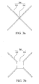
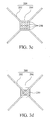
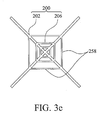
- FIGS. 3a to 3e are lead frames showing various designs of the chip carrier 206 of lead frame 200 to optimized adhesive strength among semiconductor chip 208, chip carrier 206 and the package substrate 218.
- chip carrier 206 may be an intersection area of the supporting bonds 202.
- Chip carrier 206 may have a square shape as shown in FIG. 3b .
- chip carrier 206 may have holes 250 formed inside of the chip carrier 206 as show in FIGS. 3c to 3e .
- additional supporting bonds 258 may be formed outside of the chip carrier 206, connected to supporting bonds 202, to improve adhesive strength between the chip carrier 206 and the package substrate 218.
- the holes 250 may have various kinds of shapes, for example, square, ladder, circle or the like, which are dependent upon design requirements, and is not limited.
- FIGS. 4a and 4b show one exemplary embodiment of a package substrate 218 design of a semiconductor chip package of the invention.
- the package substrate 218 not only provides amount of input/output connections of the semiconductor chip 208, but also serves as a heat sink for the semiconductor chip 208.
- the package substrate 218 may comprise a central region 220 and a marginal region 222.
- the central region 220 on the top surface 242 of the package substrate 218 is attached to and electrically connected to the second surface 234 of the chip carrier 206, having a conductive plane 227 thereon.
- the central region 220 of the package substrate 218 may provide ground paths of the semiconductor chip 208, such as, ground paths of digital circuits.
- the vias 224 in the central region 220 may be used to reduce thermal resistance.
- a plurality of conductive planes 226, 252, 256 and 258 may be disposed on the top surface 242 in the marginal region 222 of the package substrate 218, electrically connecting to some bonding pads 210 of the semiconductor chip 208 as shown in FIG. 1a , respectively.
- the conductive planes 226 and 252 may provide multiple power and/or ground paths of the semiconductor chip 208, such as, power and/or ground paths of analog circuits.
- a plurality of vias 224 is drilled through the package substrate 218, wherein some of vias 224 are electrically connected to the conductive planes 226, 227, 256 and 258.
- Each of conductive planes 226, 227, 256 and 258 may be electrically connected to a corresponding ball pad 228 (of FIG. 1b ) on the bottom surface 244 through the vias 224, respectively.
- conductive planes 256 and 258 of the package substrate 218 may provide device interface connections for transmitting data, for example, universal serial bus (USB), high definition multimedia interface (HDMI), serial advanced technology attachment (SATA) or the like.
- USB universal serial bus
- HDMI high definition multimedia interface
- SATA serial advanced technology attachment
- the conductive planes 256 and 258 in the marginal region 222 may serve differential net planes and impedance control planes of device interfaces, respectively.
- length of the bonding wires for input/output connections of the semiconductor chip 208 can be reduced to have better electrical performances, such as, reduced resistance and inductance.
- a plurality of electrical components 240 and 254 may be disposed on the package substrate 218, electrically connecting to some of the bonding pads 210 through bonding wires 212b and vias 224 as shown in FIGS. 1a and 1b .
- the aforementioned electrical components 240 and 254 may comprise passive components comprising power rings, ground rings, capacitors, resistors or inductors.
- the electrical component 240 may serve as a spiral inductor trace, and be disposed on the bottom surface 244 of the package substrate 218, electrically connecting the bonding pads 210 through the vias 245 and bonding wires 212b as shown in FIGS. 1a and 1b .
- the inductor 240 As the inductor 240 normally cannot be seen from a top view, the inductor 240 is profiled by dashed lines in FIG. 4a .
- electrical component 254 may serve as a de-coupling capacitor, and may be disposed on the top surface 242 between a ground plane and a power plane, for example, conductive planes 227 and 252.
- the de-coupling capacitor 254 may be used to reduce noise generated by circuits.
- the package substrate 218 may provide additional electrical connections for the semiconductor chip 208, for example, power and/or ground paths.
- the package substrate 218 may also provide an area for electrical components, for example, power rings, ground rings, capacitors, resistors or inductors, to be disposed thereon.
- package substrate 218 may have simple layout, for example, large power and ground planes without fine pitch traces. Therefore, fabricating cost can be reduced and yield can be improved.
- FIG. 4b illustrates an enlarged view of a portion of FIG. 4A .
- the recesses 246 may be designed at an edge of the package substrate 218, through the package substrate 218.
- the recesses 246 may be formed by firstly drilling holes (not shown) in the package substrate 218, and then sawing package substrate 218 through the holes.
- the recesses 246 may be positioned in conductive plane 252 as shown in FIG. 4b .
- the recesses 246 may provide additional electrical connection paths to the top surface 242 and bottom surface 244.
- the recesses 246 may increase surface roughness of the package substrate 218. Therefore, bonding strength between the covering material 230 and the resulting package substrate 218 can be improved.
- FIG. 5 is a flow diagram showing a fabricating process for assembly of a semiconductor chip package 500 of the invention.
- the step of assembly of a semiconductor chip package 500 comprises mounting a semiconductor chip 208 on a first surface 232 of the chip carrier 206 by adhesive material 214.
- the central region 220 of the package substrate 218 is mounted on the second surface 234 of the chip carrier 206 by an adhesive material 216, leaving the marginal region 222 exposed through the chip carrier 206.
- some bonding wires 212 are electrically connected to the bonding pads 210 and conductive planes 226 in the marginal region 222 of the package substrate 218. The remaining bonding wires 212 bond the bonding pads 210 and leads 204.
- the covering material 230 encapsulates the semiconductor chip 208, an inner portion of lead frame 200 and a portion of the package substrate 218 by molding, leaving the bottom surface 244 of the package substrate 218 exposed from the covering material 230.
- the resulting semiconductor chip package 500 is packaged for product delivery.
- the semiconductor chip package 500 is illustrated. Some advantages of an exemplary embodiment of the semiconductor chip package 500 of the invention are described in the following.
- the package substrate 218 not only serves as a heat sink for the semiconductor chip 208, but also provides amount of input/output connections of the semiconductor chip 208.
- the package substrate 218 may provide additional electrical connections for the semiconductor chip 208, for example, power and/or ground paths.
- the package substrate 218 may also provide an area for electrical components, for example, power rings, ground rings, capacitors, resistors or inductors, to be disposed thereon. Some electrical performances, for example, power circuit inductance or ground circuit inductance, can be improved.
- package substrate 218 may have simple layout.
- the vias 224 in the central region 220 may be used for reducing thermal resistance.
- the chip carrier 206 of the lead frame 200 may have various designs to optimized adhesive strength among the semiconductor chip 208, chip carrier 206 and the package substrate 218.
- a semiconductor chip package 500 is disclosed.
- the semiconductor chip package 500 comprises a lead frame 200 having a chip carrier 206, wherein the chip carrier has a first surface 232 and an opposite second surface 234.
- a semiconductor chip 208 is mounted on the first surface 232, having a plurality of bonding pads 210 thereon, wherein the semiconductor chip 208 has an area larger than that of the chip carrier 206.
- a package substrate 218 comprises a central region 220 attached to the second surface 234, having an area larger than that of the semiconductor chip 208, wherein some of the bonding pads 210 of the semiconductor chip 208 are electrically connected to a marginal region 222 of the package substrate 218.
Landscapes
- Lead Frames For Integrated Circuits (AREA)
- Semiconductor Integrated Circuits (AREA)
Abstract
Description
- The present invention relates to a semiconductor chip package, and more particularly, relates to a semiconductor chip package with an increased amount of input/output connections.
The present application claims priority under Art. 87 EPC fromU.S. Patent Application No. 12/050,210 filed on March 18, 2008 , the whole content of which is hereby incorporated by reference. - For semiconductor chip package design, an increased amount of input/output connections for multi-functional chips is required. For a conventional lead frame based semiconductor package, however, the amount of leads for input/output connections of a semiconductor chip are limited. To solve the aforementioned problem, a ball grid array (BGA) semiconductor package has been developed to provide a greater amount of input/output connections through solder balls on the bottom of a package substrate of the semiconductor chip package. Requirements for increased input/output connections can be achieved through a finer ball pitch. Compared with the conventional lead frame based semiconductor package, however, the BGA semiconductor package suffers from poorer yields and higher fabricating costs due to the additional electrical connections to the solder balls.
- A novel semiconductor chip package with an increased amount of input/output connections and fabricating cost between the fabricating cost for lead frame and BGA semiconductor packages is desirable.
- A semiconductor chip package is provided. An exemplary embodiment of the semiconductor chip package comprises a lead frame having a chip carrier, wherein the chip carrier has a first surface and an opposite second surface. A semiconductor chip is mounted on the first surface, having a plurality of bonding pads thereon, wherein the semiconductor chip has an area larger than that of the chip carrier. A package substrate comprising a central region attached to the second surface, has an area larger than that of the semiconductor chip, wherein some of the bonding pads of the semiconductor chip are electrically connected to a marginal region of the package substrate.
- Another exemplary embodiment of the semiconductor chip package comprises a lead frame having a chip carrier. A semiconductor chip is mounted on a side of the chip carrier, having a plurality of bonding pads thereon, wherein the semiconductor chip has an area larger than that of the chip carrier. A package substrate is attached on an opposite side of the chip carrier, having an area larger than that of the semiconductor chip, wherein some of the bonding pads of the semiconductor chip are electrically connected to a top surface of the package substrate, which faces the chip carrier.
- Yet another exemplary embodiment of the semiconductor chip package comprises a lead frame having a chip carrier and leads. A semiconductor chip is mounted on one side of the chip carrier, having a plurality of bonding pads thereon. A package substrate has a top surface attached on an opposite side of the chip carrier, wherein the chip carrier has an area smaller than that of the semiconductor chip and the package substrate. Some of the bonding pads are electrically connected to the top surface of the package substrate, and the remaining bonding pads are electrically connected to the leads, respectively.
- A detailed description is given in the following embodiments with reference to the accompanying drawings.
- The invention can be more fully understood by reading the subsequent detailed description and examples with references made to the accompanying drawings, wherein:
- FIG. 1a
- shows a top view of one exemplary embodiment of a semiconductor chip package of the invention.
- FIG. 1b
- shows a cross section of one exemplary embodiment of a semiconductor chip package of the invention.
- FIG. 2
- shows an assembly diagram of an exemplary embodiment of a semiconductor chip package of the invention.
- FIGS. 3a to 3e
- are lead frames showing various designs of the chip carrier.
- FIG. 4a
- shows a top view of one exemplary embodiment of a substrate of a semiconductor chip package of the invention.
- FIG. 4b
- illustrates an enlarged view of a portion of
FIG. 4A . - FIG. 5
- is a flow diagram showing a fabricating process for assembly of a semiconductor chip package of the invention.
- The following description is of a mode of carrying out the invention. This description is made for the purpose of illustrating the general principles of the invention and should not be taken in a limiting sense. The scope of the invention is best determined by reference to the appended claims. Wherever possible, the same reference numbers are used in the drawings and the descriptions to refer the same or like parts.
- In accordance with an embodiment of the present invention, embodiments of a semiconductor chip package are provided.
FIGS. 1a and 1b show one exemplary embodiment of thesemiconductor chip package 500 of the invention.FIG. 2 shows an assembly diagram of an exemplary embodiment of thesemiconductor chip package 500. In one embodiment of the invention,semiconductor chip package 500 may comprise a low-profile quad flat package (LQFP).Semiconductor chip package 500 comprises alead frame 200 comprising a plurality ofdiscrete leads 204, supportingbonds 202 and achip carrier 206.Chip carrier 206 is disposed in a central portion oflead frame 200, electrically connecting to supportingbonds 202.Chip carrier 206 has afirst surface 232 and an oppositesecond surface 234. - A
semiconductor chip 208 is mounted on thefirst surface 232 by anadhesive material 214.Semiconductor chip 208 has a plurality ofbonding pads 210 thereon. In one embodiment of the invention, thebonding pads 210 may be positioned to adjacent edges of thesemiconductor chip 208 as shown inFIG. 1a . As shown inFIGS. 1a and 1b , thesemiconductor chip 208 may have an area larger than that of thechip carrier 206. - A
package substrate 218 comprises acentral region 220 and amarginal region 222, whereincentral region 220 is attached to asecond surface 234 of thechip carrier 206 by anadhesive material 216, leaving themarginal region 222 exposed through thechip carrier 206. In one embodiment of the invention, thepackage substrate 218 may comprise a ball grid array (BGA) substrate. Thepackage substrate 218 has atop surface 242 and abottom surface 244, wherein thetop surface 242 faces asecond surface 234 of thechip carrier 206. In one embodiment of the invention,package substrate 218 may have an area larger than that of thesemiconductor chip 208. A plurality ofconductive planes top surface 242 in themarginal region 222, and aconductive plane 227 may be formed on thetop surface 242 in thecentral region 220. A plurality ofvias 224 are drilled through thepackage substrate 218, wherein some of thevias 224 are electrically connected toconductive planes semiconductor chip package 500 may further compriserecesses 246 at an edge of thepackage substrate 218, through thepackage substrate 218. Therecesses 246 may be positioned in theconductive plane 252. As shown inFIG. 1b , a plurality ofball pads 228 on abottom surface 244 of thepackage substrate 218, is electrically connected to thevias 224. In one embodiment of the invention, each ofconductive planes corresponding ball pad 228 throughvias 224, respectively. Thesemiconductor chip package 500 may further comprise solder balls (not shown) formed on theball pads 228 to provide interconnection to an underlying printed circuit board (PCB) (not shown) of a final product. - As shown in
FIGS. 1a and 1b , some of thebonding pads 210, for example,bonding pads 210 positioned adjacent to edges of thesemiconductor chip 208, are electrically connected toconductive planes 226 in themarginal region 222 of thepackage substrate 218 bybonding wires 212a, respectively. And the remainingbonding pads 210, for example,bonding pads 210 positioned away from thesemiconductor chip 208, are electrically connected to theleads 204 bybonding wires 212a, respectively. For electrical connections ofbonding wires 212b between thesemiconductor chip 208 and thepackage substrate 218,chip carrier 206 may have an area smaller than that of thesemiconductor chip 208 and thepackage substrate 218, and thepackage substrate 218 may have an area larger than that of thesemiconductor chip 208. A coveringmaterial 230 may encapsulate thesemiconductor chip 208, an inner portion oflead frame 200 and a portion of thepackage substrate 218 by such as mold filling, leaving thebottom surface 244 of thepackage substrate 218 exposed from the coveringmaterial 230. -
FIGS. 3a to 3e are lead frames showing various designs of thechip carrier 206 oflead frame 200 to optimized adhesive strength amongsemiconductor chip 208,chip carrier 206 and thepackage substrate 218. As shown inFIG. 3a ,chip carrier 206 may be an intersection area of the supportingbonds 202.Chip carrier 206 may have a square shape as shown inFIG. 3b . In some embodiments of the invention,chip carrier 206 may haveholes 250 formed inside of thechip carrier 206 as show inFIGS. 3c to 3e . Alternatively, additional supportingbonds 258 may be formed outside of thechip carrier 206, connected to supportingbonds 202, to improve adhesive strength between thechip carrier 206 and thepackage substrate 218. Theholes 250 may have various kinds of shapes, for example, square, ladder, circle or the like, which are dependent upon design requirements, and is not limited. -
FIGS. 4a and 4b show one exemplary embodiment of apackage substrate 218 design of a semiconductor chip package of the invention. Thepackage substrate 218 not only provides amount of input/output connections of thesemiconductor chip 208, but also serves as a heat sink for thesemiconductor chip 208. Thepackage substrate 218 may comprise acentral region 220 and amarginal region 222. Thecentral region 220 on thetop surface 242 of thepackage substrate 218 is attached to and electrically connected to thesecond surface 234 of thechip carrier 206, having aconductive plane 227 thereon. In one embodiment of the invention, thecentral region 220 of thepackage substrate 218 may provide ground paths of thesemiconductor chip 208, such as, ground paths of digital circuits. Also, thevias 224 in thecentral region 220 may be used to reduce thermal resistance. Also, a plurality ofconductive planes top surface 242 in themarginal region 222 of thepackage substrate 218, electrically connecting to somebonding pads 210 of thesemiconductor chip 208 as shown inFIG. 1a , respectively. In one embodiment of the invention, theconductive planes semiconductor chip 208, such as, power and/or ground paths of analog circuits. A plurality ofvias 224 is drilled through thepackage substrate 218, wherein some ofvias 224 are electrically connected to theconductive planes conductive planes FIG. 1b ) on thebottom surface 244 through thevias 224, respectively. - Additionally,
conductive planes package substrate 218 may provide device interface connections for transmitting data, for example, universal serial bus (USB), high definition multimedia interface (HDMI), serial advanced technology attachment (SATA) or the like. As shown inFIG. 4a , theconductive planes marginal region 222 may serve differential net planes and impedance control planes of device interfaces, respectively. Compared with the conventional lead frame based semiconductor package, length of the bonding wires for input/output connections of thesemiconductor chip 208 can be reduced to have better electrical performances, such as, reduced resistance and inductance. - Further, a plurality of
electrical components 240 and 254 may be disposed on thepackage substrate 218, electrically connecting to some of thebonding pads 210 throughbonding wires 212b and vias 224 as shown inFIGS. 1a and 1b . The aforementionedelectrical components 240 and 254 may comprise passive components comprising power rings, ground rings, capacitors, resistors or inductors. For example, the electrical component 240, may serve as a spiral inductor trace, and be disposed on thebottom surface 244 of thepackage substrate 218, electrically connecting thebonding pads 210 through thevias 245 andbonding wires 212b as shown inFIGS. 1a and 1b . As the inductor 240 normally cannot be seen from a top view, the inductor 240 is profiled by dashed lines inFIG. 4a . Additionally,electrical component 254, may serve as a de-coupling capacitor, and may be disposed on thetop surface 242 between a ground plane and a power plane, for example,conductive planes de-coupling capacitor 254 may be used to reduce noise generated by circuits. Compared with a conventional lead frame based semiconductor package, thepackage substrate 218 may provide additional electrical connections for thesemiconductor chip 208, for example, power and/or ground paths. Thepackage substrate 218 may also provide an area for electrical components, for example, power rings, ground rings, capacitors, resistors or inductors, to be disposed thereon. Some electrical performances, for example, power circuit inductance or ground circuit inductance, can be improved. Compared with the conventional ball grid array semiconductor package,package substrate 218 may have simple layout, for example, large power and ground planes without fine pitch traces. Therefore, fabricating cost can be reduced and yield can be improved. -
FIG. 4b illustrates an enlarged view of a portion ofFIG. 4A . In one embodiment of the invention, therecesses 246 may be designed at an edge of thepackage substrate 218, through thepackage substrate 218. Therecesses 246 may be formed by firstly drilling holes (not shown) in thepackage substrate 218, and then sawingpackage substrate 218 through the holes. Therecesses 246 may be positioned inconductive plane 252 as shown inFIG. 4b . Therecesses 246 may provide additional electrical connection paths to thetop surface 242 andbottom surface 244. Also, therecesses 246 may increase surface roughness of thepackage substrate 218. Therefore, bonding strength between the coveringmaterial 230 and the resultingpackage substrate 218 can be improved. -
FIG. 5 is a flow diagram showing a fabricating process for assembly of asemiconductor chip package 500 of the invention. As shown instep 1502, the step of assembly of asemiconductor chip package 500 comprises mounting asemiconductor chip 208 on afirst surface 232 of thechip carrier 206 byadhesive material 214. As shown instep 1504, thecentral region 220 of thepackage substrate 218 is mounted on thesecond surface 234 of thechip carrier 206 by anadhesive material 216, leaving themarginal region 222 exposed through thechip carrier 206. As shown instep 1506, somebonding wires 212 are electrically connected to thebonding pads 210 andconductive planes 226 in themarginal region 222 of thepackage substrate 218. The remainingbonding wires 212 bond thebonding pads 210 and leads 204. As shown instep 1508, the coveringmaterial 230 encapsulates thesemiconductor chip 208, an inner portion oflead frame 200 and a portion of thepackage substrate 218 by molding, leaving thebottom surface 244 of thepackage substrate 218 exposed from the coveringmaterial 230. As shown instep 1510, the resultingsemiconductor chip package 500 is packaged for product delivery. - The
semiconductor chip package 500 is illustrated. Some advantages of an exemplary embodiment of thesemiconductor chip package 500 of the invention are described in the following. Thepackage substrate 218 not only serves as a heat sink for thesemiconductor chip 208, but also provides amount of input/output connections of thesemiconductor chip 208. Compared with the conventional lead frame based semiconductor package, thepackage substrate 218 may provide additional electrical connections for thesemiconductor chip 208, for example, power and/or ground paths. Thepackage substrate 218 may also provide an area for electrical components, for example, power rings, ground rings, capacitors, resistors or inductors, to be disposed thereon. Some electrical performances, for example, power circuit inductance or ground circuit inductance, can be improved. Compared with the conventional ball grid array semiconductor package,package substrate 218 may have simple layout. Therefore, fabricating cost can be reduced and yield can be improved. Thevias 224 in thecentral region 220 may be used for reducing thermal resistance. Thechip carrier 206 of thelead frame 200 may have various designs to optimized adhesive strength among thesemiconductor chip 208,chip carrier 206 and thepackage substrate 218.
In summary asemiconductor chip package 500 is disclosed. Thesemiconductor chip package 500 comprises alead frame 200 having achip carrier 206, wherein the chip carrier has afirst surface 232 and an oppositesecond surface 234. Asemiconductor chip 208 is mounted on thefirst surface 232, having a plurality ofbonding pads 210 thereon, wherein thesemiconductor chip 208 has an area larger than that of thechip carrier 206. Apackage substrate 218 comprises acentral region 220 attached to thesecond surface 234, having an area larger than that of thesemiconductor chip 208, wherein some of thebonding pads 210 of thesemiconductor chip 208 are electrically connected to amarginal region 222 of thepackage substrate 218. - While the invention has been described by way of example and in terms of the preferred embodiments, it is to be understood that the invention is not limited to the disclosed embodiments. To the contrary, it is intended to cover various modifications and similar arrangements (as would be apparent to those skilled in the art). Therefore, the scope of the appended claims should be accorded the broadest interpretation so as to encompass all such modifications and similar arrangements.
Claims (9)
- A semiconductor chip package (500), comprising:a lead frame (200) having a chip carrier (206), wherein the chip carrier has a first surface (232) and an opposite second surface (234);a semiconductor chip (208) mounted on the first surface (232), having a plurality of bonding pads (210) thereon, wherein the semiconductor chip (208) has an area larger than that of the chip carrier (206); anda package substrate (218) comprising a central region (220) attached to the second surface (234), having an area larger than that of the semiconductor chip (208), wherein some of the bonding pads (210) of the semiconductor chip (208) are electrically connected to a marginal region (222) of the package substrate (218).
- The semiconductor chip package (500) as claimed in claim 1, wherein some of the bonding pads (210) of the semiconductor chip (208) are electrically connected to a top surface (242) of the package substrate, which faces the second surface (234) of the chip carrier.
- The semiconductor chip package (500) as claimed in claim 1, wherein the lead frame (200) comprises a plurality of leads (204), and at least one lead is electrically connected to the bonding pad, respectively.
- The semiconductor chip package (500) as claimed in claim 1, further comprising holes (250) formed inside of the chip carrier (206).
- The semiconductor chip package (500) as claimed in claim 2, further comprising:a plurality of conductive planes (226, 227, 252) on the top surface (242) in the marginal region (222), electrically connected to the bonding pads (210) of the semiconductor chip (208);a plurality of vias (224) drilled through the package substrate (218), wherein some of the vias are electrically connected to the conductive planes; anda plurality of electrical components (240, 254) on the package substrate (218),electrically connected to some of the bonding pads (210).
- The semiconductor chip package (500) as claimed in claim 5, further comprising a recess (246) at an edge of the package substrate (218), positioned in one of the conductive planes.
- The semiconductor chip package (500) as claimed in claim 5, wherein the conductive planes (226, 227, 252) comprise power planes or ground planes.
- The semiconductor chip package (500) as claimed in claim 5, wherein the electrical components (240, 254) comprise power rings, ground rings, inductor traces, capacitors, resistors, diodes or inductors.
- The semiconductor chip package (500) as claimed in claim 1, further comprising:a covering material (230) encapsulating the semiconductor chip (208), an inner portion of the lead frame (200) and a portion of the package substrate (218), leaving a bottom surface of the package substrate exposed from the covering material.
Applications Claiming Priority (1)
| Application Number | Priority Date | Filing Date | Title |
|---|---|---|---|
| US12/050,210 US7875965B2 (en) | 2008-03-18 | 2008-03-18 | Semiconductor chip package |
Publications (3)
| Publication Number | Publication Date |
|---|---|
| EP2104142A2 true EP2104142A2 (en) | 2009-09-23 |
| EP2104142A3 EP2104142A3 (en) | 2010-10-13 |
| EP2104142B1 EP2104142B1 (en) | 2016-11-02 |
Family
ID=40751494
Family Applications (1)
| Application Number | Title | Priority Date | Filing Date |
|---|---|---|---|
| EP08103752.5A Not-in-force EP2104142B1 (en) | 2008-03-18 | 2008-04-28 | Semiconductor chip package |
Country Status (4)
| Country | Link |
|---|---|
| US (1) | US7875965B2 (en) |
| EP (1) | EP2104142B1 (en) |
| CN (2) | CN101540308B (en) |
| TW (1) | TWI377657B (en) |
Families Citing this family (14)
| Publication number | Priority date | Publication date | Assignee | Title |
|---|---|---|---|---|
| US20090256245A1 (en) * | 2008-04-14 | 2009-10-15 | Yong Liu | Stacked Micro-Module Packages, Systems Using the Same, and Methods of Making the Same |
| US20090315163A1 (en) * | 2008-06-20 | 2009-12-24 | Terry Johnson | Semiconductor Die Packages with Stacked Flexible Modules Having Passive Components, Systems Using the Same, and Methods of Making the Same |
| US20090315162A1 (en) * | 2008-06-20 | 2009-12-24 | Yong Liu | Micro-Modules with Molded Passive Components, Systems Using the Same, and Methods of Making the Same |
| US8018037B2 (en) * | 2009-04-16 | 2011-09-13 | Mediatek Inc. | Semiconductor chip package |
| US20100295160A1 (en) * | 2009-05-22 | 2010-11-25 | Advanced Semiconductor Engineering, Inc. | Quad flat package structure having exposed heat sink, electronic assembly and manufacturing methods thereof |
| TWI420626B (en) * | 2009-07-01 | 2013-12-21 | 日月光半導體製造股份有限公司 | Package structure and packaging process |
| CN102215043A (en) * | 2010-04-09 | 2011-10-12 | 国民技术股份有限公司 | Wireless communication module |
| US9158883B2 (en) * | 2012-08-08 | 2015-10-13 | Taiwan Semiconductor Manufacturing Company, Ltd. | System for designing a semiconductor device, device made, and method of using the system |
| CN103531579B (en) * | 2013-11-06 | 2017-04-05 | 北京思比科微电子技术股份有限公司 | A kind of structure for improving semiconductor die package reliability and preparation method thereof |
| WO2017105446A1 (en) * | 2015-12-16 | 2017-06-22 | Intel Corporation | Improved package power delivery using plane and shaped vias |
| US11056455B2 (en) * | 2017-08-01 | 2021-07-06 | Analog Devices, Inc. | Negative fillet for mounting an integrated device die to a carrier |
| CN109982501A (en) * | 2017-12-28 | 2019-07-05 | 中兴通讯股份有限公司 | Signal transmission board |
| CN114035387B (en) * | 2021-11-30 | 2023-08-25 | 绵阳惠科光电科技有限公司 | Array substrate and display panel |
| CN117253871B (en) * | 2023-11-20 | 2024-02-13 | 佛山市蓝箭电子股份有限公司 | Semiconductor packaging device and packaging method thereof |
Citations (3)
| Publication number | Priority date | Publication date | Assignee | Title |
|---|---|---|---|---|
| JPS6114731A (en) | 1984-06-29 | 1986-01-22 | Nec Kansai Ltd | Semiconductor device |
| JPH07297348A (en) | 1994-04-21 | 1995-11-10 | Hitachi Ltd | SEMICONDUCTOR DEVICE, LEAD FRAME USED IN MANUFACTURING THE SAME, AND SEMICONDUCTOR DEVICE MANUFACTURING METHOD |
| US20030214023A1 (en) | 2002-05-15 | 2003-11-20 | Yasufumi Uchida | Semiconductor device having multi-chip package |
Family Cites Families (17)
| Publication number | Priority date | Publication date | Assignee | Title |
|---|---|---|---|---|
| JP2623980B2 (en) | 1991-01-30 | 1997-06-25 | 日立化成工業株式会社 | Manufacturing method of substrate with lead for semiconductor mounting |
| JPH06163794A (en) | 1992-11-19 | 1994-06-10 | Shinko Electric Ind Co Ltd | Metal core type multilayer lead frame |
| DE69430648T2 (en) | 1993-03-22 | 2002-10-24 | Motorola, Inc. | Semiconductor arrangement consisting of an X-shaped mounting frame and its manufacturing process |
| JPH0766331A (en) * | 1993-08-02 | 1995-03-10 | Motorola Inc | Method of manufacturing semiconductor device package |
| US5563446A (en) | 1994-01-25 | 1996-10-08 | Lsi Logic Corporation | Surface mount peripheral leaded and ball grid array package |
| JPH0837252A (en) | 1994-07-22 | 1996-02-06 | Nec Corp | Semiconductor device |
| US5508556A (en) | 1994-09-02 | 1996-04-16 | Motorola, Inc. | Leaded semiconductor device having accessible power supply pad terminals |
| JPH09153586A (en) * | 1995-12-01 | 1997-06-10 | Texas Instr Japan Ltd | Semiconductor device, manufacturing method thereof, and lead frame |
| JP2000058739A (en) | 1998-08-10 | 2000-02-25 | Hitachi Ltd | Semiconductor device and lead frame used for manufacturing the same |
| JP3429245B2 (en) * | 2000-03-07 | 2003-07-22 | 沖電気工業株式会社 | Semiconductor device and manufacturing method thereof |
| US6545345B1 (en) * | 2001-03-20 | 2003-04-08 | Amkor Technology, Inc. | Mounting for a package containing a chip |
| CN2585407Y (en) | 2002-11-11 | 2003-11-05 | 矽统科技股份有限公司 | Packaging substrate for improving wire punching and manufactured package |
| JP4245466B2 (en) | 2003-12-04 | 2009-03-25 | Necエレクトロニクス株式会社 | Noise removal circuit |
| CN101142675B (en) * | 2005-02-23 | 2013-01-02 | 泰萨拉知识产权公司 | An integrated circuit package device with improved bond pad connections, a leadframe and an electronic device |
| US7384819B2 (en) * | 2006-04-28 | 2008-06-10 | Freescale Semiconductor, Inc. | Method of forming stackable package |
| US8183680B2 (en) * | 2006-05-16 | 2012-05-22 | Broadcom Corporation | No-lead IC packages having integrated heat spreader for electromagnetic interference (EMI) shielding and thermal enhancement |
| US7872335B2 (en) * | 2007-06-08 | 2011-01-18 | Broadcom Corporation | Lead frame-BGA package with enhanced thermal performance and I/O counts |
-
2008
- 2008-03-18 US US12/050,210 patent/US7875965B2/en active Active
- 2008-04-28 EP EP08103752.5A patent/EP2104142B1/en not_active Not-in-force
- 2008-07-22 CN CN2008101322539A patent/CN101540308B/en not_active Expired - Fee Related
- 2008-07-25 TW TW097128331A patent/TWI377657B/en not_active IP Right Cessation
-
2009
- 2009-03-16 CN CN2009101194592A patent/CN101540304B/en not_active Expired - Fee Related
Patent Citations (3)
| Publication number | Priority date | Publication date | Assignee | Title |
|---|---|---|---|---|
| JPS6114731A (en) | 1984-06-29 | 1986-01-22 | Nec Kansai Ltd | Semiconductor device |
| JPH07297348A (en) | 1994-04-21 | 1995-11-10 | Hitachi Ltd | SEMICONDUCTOR DEVICE, LEAD FRAME USED IN MANUFACTURING THE SAME, AND SEMICONDUCTOR DEVICE MANUFACTURING METHOD |
| US20030214023A1 (en) | 2002-05-15 | 2003-11-20 | Yasufumi Uchida | Semiconductor device having multi-chip package |
Also Published As
| Publication number | Publication date |
|---|---|
| CN101540308A (en) | 2009-09-23 |
| EP2104142A3 (en) | 2010-10-13 |
| US7875965B2 (en) | 2011-01-25 |
| CN101540304A (en) | 2009-09-23 |
| US20090236709A1 (en) | 2009-09-24 |
| TW200941683A (en) | 2009-10-01 |
| CN101540308B (en) | 2010-12-08 |
| CN101540304B (en) | 2011-05-18 |
| EP2104142B1 (en) | 2016-11-02 |
| TWI377657B (en) | 2012-11-21 |
Similar Documents
| Publication | Publication Date | Title |
|---|---|---|
| US7875965B2 (en) | Semiconductor chip package | |
| US8212343B2 (en) | Semiconductor chip package | |
| US8288848B2 (en) | Semiconductor chip package including a lead frame | |
| JP5514560B2 (en) | Semiconductor device | |
| USRE42653E1 (en) | Semiconductor package with heat dissipating structure | |
| US8860201B1 (en) | Stacked integrated circuit package using a window substrate | |
| US20050104196A1 (en) | Semiconductor package | |
| US20090108422A1 (en) | Semiconductor device | |
| KR20010034526A (en) | Low profile ball grid array package | |
| EP1155448A1 (en) | Leadless chip carrier design and structure | |
| EP1911092B1 (en) | Integrated circuit packaging | |
| US7091607B2 (en) | Semiconductor package | |
| WO2013098929A1 (en) | Semiconductor chip and semiconductor module mounted with same | |
| JP2001168233A (en) | Multi-line grid array package | |
| US7863716B2 (en) | Method and apparatus of power ring positioning to minimize crosstalk | |
| JP2007053121A (en) | Semiconductor device, stacked semiconductor device, and wiring board | |
| CN102237324A (en) | Integrated circuit packaging structure and method | |
| US20090253230A1 (en) | Method for manufacturing stack chip package structure | |
| JPH10173087A (en) | Semiconductor integrated circuit device | |
| JP2012084817A (en) | Semiconductor device | |
| US11239141B2 (en) | Lead frame package | |
| KR20030012192A (en) | A window chip scale package having stacked dies | |
| JP2014123783A (en) | Semiconductor device |
Legal Events
| Date | Code | Title | Description |
|---|---|---|---|
| PUAI | Public reference made under article 153(3) epc to a published international application that has entered the european phase |
Free format text: ORIGINAL CODE: 0009012 |
|
| AK | Designated contracting states |
Kind code of ref document: A2 Designated state(s): AT BE BG CH CY CZ DE DK EE ES FI FR GB GR HR HU IE IS IT LI LT LU LV MC MT NL NO PL PT RO SE SI SK TR |
|
| AX | Request for extension of the european patent |
Extension state: AL BA MK RS |
|
| PUAL | Search report despatched |
Free format text: ORIGINAL CODE: 0009013 |
|
| AK | Designated contracting states |
Kind code of ref document: A3 Designated state(s): AT BE BG CH CY CZ DE DK EE ES FI FR GB GR HR HU IE IS IT LI LT LU LV MC MT NL NO PL PT RO SE SI SK TR |
|
| AX | Request for extension of the european patent |
Extension state: AL BA MK RS |
|
| AKY | No designation fees paid | ||
| 17P | Request for examination filed |
Effective date: 20110411 |
|
| RBV | Designated contracting states (corrected) |
Designated state(s): AT BE BG CH CY CZ LI |
|
| RBV | Designated contracting states (corrected) |
Designated state(s): AT BE BG CH CY CZ DE DK EE ES FI FR GB GR HR HU IE IS IT LI LT LU LV MC MT NL NO PL PT RO SE SI SK TR |
|
| REG | Reference to a national code |
Ref country code: DE Ref legal event code: R108 Ref document number: 602008047131 Country of ref document: DE Effective date: 20110607 Ref country code: DE Ref legal event code: R108 Effective date: 20110607 |
|
| 17Q | First examination report despatched |
Effective date: 20131024 |
|
| GRAP | Despatch of communication of intention to grant a patent |
Free format text: ORIGINAL CODE: EPIDOSNIGR1 |
|
| INTG | Intention to grant announced |
Effective date: 20160527 |
|
| GRAS | Grant fee paid |
Free format text: ORIGINAL CODE: EPIDOSNIGR3 |
|
| GRAA | (expected) grant |
Free format text: ORIGINAL CODE: 0009210 |
|
| AK | Designated contracting states |
Kind code of ref document: B1 Designated state(s): AT BE BG CH CY CZ DE DK EE ES FI FR GB GR HR HU IE IS IT LI LT LU LV MC MT NL NO PL PT RO SE SI SK TR |
|
| REG | Reference to a national code |
Ref country code: GB Ref legal event code: FG4D |
|
| REG | Reference to a national code |
Ref country code: AT Ref legal event code: REF Ref document number: 842611 Country of ref document: AT Kind code of ref document: T Effective date: 20161115 Ref country code: CH Ref legal event code: EP |
|
| REG | Reference to a national code |
Ref country code: IE Ref legal event code: FG4D |
|
| REG | Reference to a national code |
Ref country code: DE Ref legal event code: R096 Ref document number: 602008047131 Country of ref document: DE |
|
| PG25 | Lapsed in a contracting state [announced via postgrant information from national office to epo] |
Ref country code: LV Free format text: LAPSE BECAUSE OF FAILURE TO SUBMIT A TRANSLATION OF THE DESCRIPTION OR TO PAY THE FEE WITHIN THE PRESCRIBED TIME-LIMIT Effective date: 20161102 |
|
| REG | Reference to a national code |
Ref country code: NL Ref legal event code: MP Effective date: 20161102 |
|
| REG | Reference to a national code |
Ref country code: LT Ref legal event code: MG4D |
|
| REG | Reference to a national code |
Ref country code: AT Ref legal event code: MK05 Ref document number: 842611 Country of ref document: AT Kind code of ref document: T Effective date: 20161102 |
|
| REG | Reference to a national code |
Ref country code: FR Ref legal event code: PLFP Year of fee payment: 10 |
|
| PG25 | Lapsed in a contracting state [announced via postgrant information from national office to epo] |
Ref country code: NO Free format text: LAPSE BECAUSE OF FAILURE TO SUBMIT A TRANSLATION OF THE DESCRIPTION OR TO PAY THE FEE WITHIN THE PRESCRIBED TIME-LIMIT Effective date: 20170202 Ref country code: NL Free format text: LAPSE BECAUSE OF FAILURE TO SUBMIT A TRANSLATION OF THE DESCRIPTION OR TO PAY THE FEE WITHIN THE PRESCRIBED TIME-LIMIT Effective date: 20161102 Ref country code: GR Free format text: LAPSE BECAUSE OF FAILURE TO SUBMIT A TRANSLATION OF THE DESCRIPTION OR TO PAY THE FEE WITHIN THE PRESCRIBED TIME-LIMIT Effective date: 20170203 Ref country code: SE Free format text: LAPSE BECAUSE OF FAILURE TO SUBMIT A TRANSLATION OF THE DESCRIPTION OR TO PAY THE FEE WITHIN THE PRESCRIBED TIME-LIMIT Effective date: 20161102 Ref country code: LT Free format text: LAPSE BECAUSE OF FAILURE TO SUBMIT A TRANSLATION OF THE DESCRIPTION OR TO PAY THE FEE WITHIN THE PRESCRIBED TIME-LIMIT Effective date: 20161102 |
|
| PG25 | Lapsed in a contracting state [announced via postgrant information from national office to epo] |
Ref country code: ES Free format text: LAPSE BECAUSE OF FAILURE TO SUBMIT A TRANSLATION OF THE DESCRIPTION OR TO PAY THE FEE WITHIN THE PRESCRIBED TIME-LIMIT Effective date: 20161102 Ref country code: PL Free format text: LAPSE BECAUSE OF FAILURE TO SUBMIT A TRANSLATION OF THE DESCRIPTION OR TO PAY THE FEE WITHIN THE PRESCRIBED TIME-LIMIT Effective date: 20161102 Ref country code: AT Free format text: LAPSE BECAUSE OF FAILURE TO SUBMIT A TRANSLATION OF THE DESCRIPTION OR TO PAY THE FEE WITHIN THE PRESCRIBED TIME-LIMIT Effective date: 20161102 Ref country code: FI Free format text: LAPSE BECAUSE OF FAILURE TO SUBMIT A TRANSLATION OF THE DESCRIPTION OR TO PAY THE FEE WITHIN THE PRESCRIBED TIME-LIMIT Effective date: 20161102 Ref country code: IS Free format text: LAPSE BECAUSE OF FAILURE TO SUBMIT A TRANSLATION OF THE DESCRIPTION OR TO PAY THE FEE WITHIN THE PRESCRIBED TIME-LIMIT Effective date: 20170302 Ref country code: PT Free format text: LAPSE BECAUSE OF FAILURE TO SUBMIT A TRANSLATION OF THE DESCRIPTION OR TO PAY THE FEE WITHIN THE PRESCRIBED TIME-LIMIT Effective date: 20170302 Ref country code: HR Free format text: LAPSE BECAUSE OF FAILURE TO SUBMIT A TRANSLATION OF THE DESCRIPTION OR TO PAY THE FEE WITHIN THE PRESCRIBED TIME-LIMIT Effective date: 20161102 |
|
| PG25 | Lapsed in a contracting state [announced via postgrant information from national office to epo] |
Ref country code: CZ Free format text: LAPSE BECAUSE OF FAILURE TO SUBMIT A TRANSLATION OF THE DESCRIPTION OR TO PAY THE FEE WITHIN THE PRESCRIBED TIME-LIMIT Effective date: 20161102 Ref country code: DK Free format text: LAPSE BECAUSE OF FAILURE TO SUBMIT A TRANSLATION OF THE DESCRIPTION OR TO PAY THE FEE WITHIN THE PRESCRIBED TIME-LIMIT Effective date: 20161102 Ref country code: EE Free format text: LAPSE BECAUSE OF FAILURE TO SUBMIT A TRANSLATION OF THE DESCRIPTION OR TO PAY THE FEE WITHIN THE PRESCRIBED TIME-LIMIT Effective date: 20161102 Ref country code: RO Free format text: LAPSE BECAUSE OF FAILURE TO SUBMIT A TRANSLATION OF THE DESCRIPTION OR TO PAY THE FEE WITHIN THE PRESCRIBED TIME-LIMIT Effective date: 20161102 Ref country code: SK Free format text: LAPSE BECAUSE OF FAILURE TO SUBMIT A TRANSLATION OF THE DESCRIPTION OR TO PAY THE FEE WITHIN THE PRESCRIBED TIME-LIMIT Effective date: 20161102 |
|
| REG | Reference to a national code |
Ref country code: DE Ref legal event code: R097 Ref document number: 602008047131 Country of ref document: DE |
|
| PG25 | Lapsed in a contracting state [announced via postgrant information from national office to epo] |
Ref country code: IT Free format text: LAPSE BECAUSE OF FAILURE TO SUBMIT A TRANSLATION OF THE DESCRIPTION OR TO PAY THE FEE WITHIN THE PRESCRIBED TIME-LIMIT Effective date: 20161102 Ref country code: BE Free format text: LAPSE BECAUSE OF FAILURE TO SUBMIT A TRANSLATION OF THE DESCRIPTION OR TO PAY THE FEE WITHIN THE PRESCRIBED TIME-LIMIT Effective date: 20161102 |
|
| PLBE | No opposition filed within time limit |
Free format text: ORIGINAL CODE: 0009261 |
|
| STAA | Information on the status of an ep patent application or granted ep patent |
Free format text: STATUS: NO OPPOSITION FILED WITHIN TIME LIMIT |
|
| 26N | No opposition filed |
Effective date: 20170803 |
|
| PG25 | Lapsed in a contracting state [announced via postgrant information from national office to epo] |
Ref country code: SI Free format text: LAPSE BECAUSE OF FAILURE TO SUBMIT A TRANSLATION OF THE DESCRIPTION OR TO PAY THE FEE WITHIN THE PRESCRIBED TIME-LIMIT Effective date: 20161102 |
|
| REG | Reference to a national code |
Ref country code: CH Ref legal event code: PL |
|
| REG | Reference to a national code |
Ref country code: IE Ref legal event code: MM4A |
|
| PG25 | Lapsed in a contracting state [announced via postgrant information from national office to epo] |
Ref country code: MC Free format text: LAPSE BECAUSE OF FAILURE TO SUBMIT A TRANSLATION OF THE DESCRIPTION OR TO PAY THE FEE WITHIN THE PRESCRIBED TIME-LIMIT Effective date: 20161102 |
|
| PG25 | Lapsed in a contracting state [announced via postgrant information from national office to epo] |
Ref country code: CH Free format text: LAPSE BECAUSE OF NON-PAYMENT OF DUE FEES Effective date: 20170430 Ref country code: LU Free format text: LAPSE BECAUSE OF NON-PAYMENT OF DUE FEES Effective date: 20170428 Ref country code: LI Free format text: LAPSE BECAUSE OF NON-PAYMENT OF DUE FEES Effective date: 20170430 |
|
| REG | Reference to a national code |
Ref country code: FR Ref legal event code: PLFP Year of fee payment: 11 |
|
| PG25 | Lapsed in a contracting state [announced via postgrant information from national office to epo] |
Ref country code: IE Free format text: LAPSE BECAUSE OF NON-PAYMENT OF DUE FEES Effective date: 20170428 |
|
| PG25 | Lapsed in a contracting state [announced via postgrant information from national office to epo] |
Ref country code: MT Free format text: LAPSE BECAUSE OF NON-PAYMENT OF DUE FEES Effective date: 20170428 |
|
| PG25 | Lapsed in a contracting state [announced via postgrant information from national office to epo] |
Ref country code: HU Free format text: LAPSE BECAUSE OF FAILURE TO SUBMIT A TRANSLATION OF THE DESCRIPTION OR TO PAY THE FEE WITHIN THE PRESCRIBED TIME-LIMIT; INVALID AB INITIO Effective date: 20080428 |
|
| PG25 | Lapsed in a contracting state [announced via postgrant information from national office to epo] |
Ref country code: BG Free format text: LAPSE BECAUSE OF FAILURE TO SUBMIT A TRANSLATION OF THE DESCRIPTION OR TO PAY THE FEE WITHIN THE PRESCRIBED TIME-LIMIT Effective date: 20161102 |
|
| PG25 | Lapsed in a contracting state [announced via postgrant information from national office to epo] |
Ref country code: CY Free format text: LAPSE BECAUSE OF NON-PAYMENT OF DUE FEES Effective date: 20161102 |
|
| PG25 | Lapsed in a contracting state [announced via postgrant information from national office to epo] |
Ref country code: TR Free format text: LAPSE BECAUSE OF FAILURE TO SUBMIT A TRANSLATION OF THE DESCRIPTION OR TO PAY THE FEE WITHIN THE PRESCRIBED TIME-LIMIT Effective date: 20161102 |
|
| P01 | Opt-out of the competence of the unified patent court (upc) registered |
Effective date: 20230607 |
|
| PGFP | Annual fee paid to national office [announced via postgrant information from national office to epo] |
Ref country code: FR Payment date: 20230425 Year of fee payment: 16 Ref country code: DE Payment date: 20230427 Year of fee payment: 16 |
|
| PGFP | Annual fee paid to national office [announced via postgrant information from national office to epo] |
Ref country code: GB Payment date: 20230427 Year of fee payment: 16 |
|
| REG | Reference to a national code |
Ref country code: DE Ref legal event code: R119 Ref document number: 602008047131 Country of ref document: DE |
|
| GBPC | Gb: european patent ceased through non-payment of renewal fee |
Effective date: 20240428 |
|
| PG25 | Lapsed in a contracting state [announced via postgrant information from national office to epo] |
Ref country code: DE Free format text: LAPSE BECAUSE OF NON-PAYMENT OF DUE FEES Effective date: 20241105 |
|
| PG25 | Lapsed in a contracting state [announced via postgrant information from national office to epo] |
Ref country code: GB Free format text: LAPSE BECAUSE OF NON-PAYMENT OF DUE FEES Effective date: 20240428 |
|
| PG25 | Lapsed in a contracting state [announced via postgrant information from national office to epo] |
Ref country code: FR Free format text: LAPSE BECAUSE OF NON-PAYMENT OF DUE FEES Effective date: 20240430 |
|
| PG25 | Lapsed in a contracting state [announced via postgrant information from national office to epo] |
Ref country code: GB Free format text: LAPSE BECAUSE OF NON-PAYMENT OF DUE FEES Effective date: 20240428 Ref country code: FR Free format text: LAPSE BECAUSE OF NON-PAYMENT OF DUE FEES Effective date: 20240430 Ref country code: DE Free format text: LAPSE BECAUSE OF NON-PAYMENT OF DUE FEES Effective date: 20241105 |