EP2102900B1 - Self-constrained anisotropic germanium nanostructure from electroplating - Google Patents
Self-constrained anisotropic germanium nanostructure from electroplating Download PDFInfo
- Publication number
- EP2102900B1 EP2102900B1 EP07857746A EP07857746A EP2102900B1 EP 2102900 B1 EP2102900 B1 EP 2102900B1 EP 07857746 A EP07857746 A EP 07857746A EP 07857746 A EP07857746 A EP 07857746A EP 2102900 B1 EP2102900 B1 EP 2102900B1
- Authority
- EP
- European Patent Office
- Prior art keywords
- substrate
- germanium
- electroplating
- semiconductor substrate
- group
- Prior art date
- Legal status (The legal status is an assumption and is not a legal conclusion. Google has not performed a legal analysis and makes no representation as to the accuracy of the status listed.)
- Not-in-force
Links
Images





Classifications
-
- C—CHEMISTRY; METALLURGY
- C25—ELECTROLYTIC OR ELECTROPHORETIC PROCESSES; APPARATUS THEREFOR
- C25D—PROCESSES FOR THE ELECTROLYTIC OR ELECTROPHORETIC PRODUCTION OF COATINGS; ELECTROFORMING; APPARATUS THEREFOR
- C25D3/00—Electroplating: Baths therefor
- C25D3/02—Electroplating: Baths therefor from solutions
- C25D3/54—Electroplating: Baths therefor from solutions of metals not provided for in groups C25D3/04 - C25D3/50
-
- C—CHEMISTRY; METALLURGY
- C25—ELECTROLYTIC OR ELECTROPHORETIC PROCESSES; APPARATUS THEREFOR
- C25D—PROCESSES FOR THE ELECTROLYTIC OR ELECTROPHORETIC PRODUCTION OF COATINGS; ELECTROFORMING; APPARATUS THEREFOR
- C25D5/00—Electroplating characterised by the process; Pretreatment or after-treatment of workpieces
- C25D5/02—Electroplating of selected surface areas
-
- B—PERFORMING OPERATIONS; TRANSPORTING
- B82—NANOTECHNOLOGY
- B82B—NANOSTRUCTURES FORMED BY MANIPULATION OF INDIVIDUAL ATOMS, MOLECULES, OR LIMITED COLLECTIONS OF ATOMS OR MOLECULES AS DISCRETE UNITS; MANUFACTURE OR TREATMENT THEREOF
- B82B3/00—Manufacture or treatment of nanostructures by manipulation of individual atoms or molecules, or limited collections of atoms or molecules as discrete units
-
- C—CHEMISTRY; METALLURGY
- C25—ELECTROLYTIC OR ELECTROPHORETIC PROCESSES; APPARATUS THEREFOR
- C25D—PROCESSES FOR THE ELECTROLYTIC OR ELECTROPHORETIC PRODUCTION OF COATINGS; ELECTROFORMING; APPARATUS THEREFOR
- C25D5/00—Electroplating characterised by the process; Pretreatment or after-treatment of workpieces
- C25D5/02—Electroplating of selected surface areas
- C25D5/022—Electroplating of selected surface areas using masking means
-
- C—CHEMISTRY; METALLURGY
- C25—ELECTROLYTIC OR ELECTROPHORETIC PROCESSES; APPARATUS THEREFOR
- C25D—PROCESSES FOR THE ELECTROLYTIC OR ELECTROPHORETIC PRODUCTION OF COATINGS; ELECTROFORMING; APPARATUS THEREFOR
- C25D7/00—Electroplating characterised by the article coated
- C25D7/12—Semiconductors
- C25D7/123—Semiconductors first coated with a seed layer or a conductive layer
-
- H—ELECTRICITY
- H10—SEMICONDUCTOR DEVICES; ELECTRIC SOLID-STATE DEVICES NOT OTHERWISE PROVIDED FOR
- H10P—GENERIC PROCESSES OR APPARATUS FOR THE MANUFACTURE OR TREATMENT OF DEVICES COVERED BY CLASS H10
- H10P14/00—Formation of materials, e.g. in the shape of layers or pillars
- H10P14/20—Formation of materials, e.g. in the shape of layers or pillars of semiconductor materials
-
- H—ELECTRICITY
- H10—SEMICONDUCTOR DEVICES; ELECTRIC SOLID-STATE DEVICES NOT OTHERWISE PROVIDED FOR
- H10P—GENERIC PROCESSES OR APPARATUS FOR THE MANUFACTURE OR TREATMENT OF DEVICES COVERED BY CLASS H10
- H10P14/00—Formation of materials, e.g. in the shape of layers or pillars
- H10P14/20—Formation of materials, e.g. in the shape of layers or pillars of semiconductor materials
- H10P14/26—Formation of materials, e.g. in the shape of layers or pillars of semiconductor materials using liquid deposition
- H10P14/265—Formation of materials, e.g. in the shape of layers or pillars of semiconductor materials using liquid deposition using solutions
-
- H—ELECTRICITY
- H10—SEMICONDUCTOR DEVICES; ELECTRIC SOLID-STATE DEVICES NOT OTHERWISE PROVIDED FOR
- H10P—GENERIC PROCESSES OR APPARATUS FOR THE MANUFACTURE OR TREATMENT OF DEVICES COVERED BY CLASS H10
- H10P14/00—Formation of materials, e.g. in the shape of layers or pillars
- H10P14/20—Formation of materials, e.g. in the shape of layers or pillars of semiconductor materials
- H10P14/27—Formation of materials, e.g. in the shape of layers or pillars of semiconductor materials using selective deposition, e.g. simultaneous growth of monocrystalline and non-monocrystalline semiconductor materials
- H10P14/271—Formation of materials, e.g. in the shape of layers or pillars of semiconductor materials using selective deposition, e.g. simultaneous growth of monocrystalline and non-monocrystalline semiconductor materials characterised by the preparation of substrate for selective deposition
-
- H—ELECTRICITY
- H10—SEMICONDUCTOR DEVICES; ELECTRIC SOLID-STATE DEVICES NOT OTHERWISE PROVIDED FOR
- H10P—GENERIC PROCESSES OR APPARATUS FOR THE MANUFACTURE OR TREATMENT OF DEVICES COVERED BY CLASS H10
- H10P14/00—Formation of materials, e.g. in the shape of layers or pillars
- H10P14/20—Formation of materials, e.g. in the shape of layers or pillars of semiconductor materials
- H10P14/29—Formation of materials, e.g. in the shape of layers or pillars of semiconductor materials characterised by the substrates
- H10P14/2901—Materials
-
- H—ELECTRICITY
- H10—SEMICONDUCTOR DEVICES; ELECTRIC SOLID-STATE DEVICES NOT OTHERWISE PROVIDED FOR
- H10P—GENERIC PROCESSES OR APPARATUS FOR THE MANUFACTURE OR TREATMENT OF DEVICES COVERED BY CLASS H10
- H10P14/00—Formation of materials, e.g. in the shape of layers or pillars
- H10P14/20—Formation of materials, e.g. in the shape of layers or pillars of semiconductor materials
- H10P14/34—Deposited materials, e.g. layers
- H10P14/3402—Deposited materials, e.g. layers characterised by the chemical composition
- H10P14/3404—Deposited materials, e.g. layers characterised by the chemical composition being Group IVA materials
- H10P14/3411—Silicon, silicon germanium or germanium
-
- H—ELECTRICITY
- H10—SEMICONDUCTOR DEVICES; ELECTRIC SOLID-STATE DEVICES NOT OTHERWISE PROVIDED FOR
- H10P—GENERIC PROCESSES OR APPARATUS FOR THE MANUFACTURE OR TREATMENT OF DEVICES COVERED BY CLASS H10
- H10P14/00—Formation of materials, e.g. in the shape of layers or pillars
- H10P14/20—Formation of materials, e.g. in the shape of layers or pillars of semiconductor materials
- H10P14/34—Deposited materials, e.g. layers
- H10P14/3451—Structure
- H10P14/3452—Microstructure
- H10P14/3462—Nanowires
-
- B—PERFORMING OPERATIONS; TRANSPORTING
- B82—NANOTECHNOLOGY
- B82Y—SPECIFIC USES OR APPLICATIONS OF NANOSTRUCTURES; MEASUREMENT OR ANALYSIS OF NANOSTRUCTURES; MANUFACTURE OR TREATMENT OF NANOSTRUCTURES
- B82Y10/00—Nanotechnology for information processing, storage or transmission, e.g. quantum computing or single electron logic
-
- Y—GENERAL TAGGING OF NEW TECHNOLOGICAL DEVELOPMENTS; GENERAL TAGGING OF CROSS-SECTIONAL TECHNOLOGIES SPANNING OVER SEVERAL SECTIONS OF THE IPC; TECHNICAL SUBJECTS COVERED BY FORMER USPC CROSS-REFERENCE ART COLLECTIONS [XRACs] AND DIGESTS
- Y10—TECHNICAL SUBJECTS COVERED BY FORMER USPC
- Y10S—TECHNICAL SUBJECTS COVERED BY FORMER USPC CROSS-REFERENCE ART COLLECTIONS [XRACs] AND DIGESTS
- Y10S977/00—Nanotechnology
- Y10S977/70—Nanostructure
- Y10S977/762—Nanowire or quantum wire, i.e. axially elongated structure having two dimensions of 100 nm or less
Definitions
- the field of the present disclosure relates to the nanostructure comprising germanium (Ge) nanowires.
- the present disclosure relates to electrodeposition of Ge onto patterned semiconductor substrates.
- Nanowire field effect transistors would allow 3-dimensional integration and thus a much higher device density than the current technologies.
- the key element of such a device is the semiconductor nanowire. So far, nanowires of a few semiconductor compounds produced by electroplating have been reported. However, nanowires of Si and Ge have only been produced by vacuum processes.
- the previously reported nanowire structures made from electroplating are produced with a template, which defines the shape of the structures.
- the template (100) with nanopores (101) has a layer of conductive material (102) at one side, which carries the electroplating current and wire structures (103) are electroplated with the shape defined by the pores.
- Germanium is a semiconducting material with higher mobility as compared to silicon.
- electrodeposition of germanium onto metals have not been especially successful. These efforts may have not been thwarted due to the high reversible potential of Ge and the very low hydrogen overpotential on Ge surfaces. Therefore, all of the plating current can result from the proton reduction (side reaction) and no Ge plating can occur once the electrode surface is covered by Ge. So far, three approaches of Ge electroplating have been reported.
- the present disclosure relates to a nanostructure that comprises a semiconductor substrate, and comprises Ge in contact with the substrate.
- the Ge is less than 1 micrometer in at least one dimension. In one embodiment the Ge extends outwardly from its substrate.
- the present disclosure also relates to a method as claimed in claim 1.
- the Ge is less than 1 micrometer in at least one dimension. In one embodiment the Ge extends outwardly from its substrate and the Ge is less than 1 micrometer in diameter.
- Suitable semiconductor conductor substrates include but not limited to: Si-based and Ge-based semiconductors such as Si, Ge, SiGe alloys, SiC alloys, SiGeC alloys as well as III-V and II-VI semiconductors as well as any combinations of the above.
- germanium nanostructures are electroplated onto patterned semiconductor substrates having insulating regions and semiconductor regions.
- the insulating regions can be formed from dielectrics such as silicon oxides, silicon nitrides and aluminum oxide.
- the germanium can be electroplated directly onto the semiconductor substrate without any seed or intermediate layer such as a seed layer.
- a seed layer such as copper or nickel layer can be deposited prior to the electroplating of the germanium.
- This seed layer can be formed prior to the fabrication of the dielectric stencil by standard deposition processes such as sputtering, evaporation, PVD and CVD.
- the seed layer is typically about 10 to about 100 nanometers thick and more typically about 10 to about 20 nanometers thick.
- Other intermediate layer can also be deposited prior to the germanium plating by electrochemical deposition including electroless or electroplating techniques.
- the electroplating bath typically employed according to the present disclosure contains a source of germanium ions such as germanium tetrahalide and especially germanium tetrachloride and an organic solvent such as an alkyl diol.
- alkyl diols are alkyl diols typically having 2-5 carbon atoms and including ethylene glycol, propylene glycol, 1,3 propanediol, butylene glycol, 1,3 butanediol and pentylene glycol.
- the concentration of the source of germanium is typically about 0.2 to about 0.7 moles and more typically about 0.3 to about 0.5 moles/liter; an example being about 0.5 mol/L GeCl 4 .
- the components of the electroplating bath are desirably highly pure (>99.9%).
- FIG. 7 shows a plating apparatus 10 that may be used to implement the Ge electroplating of the present disclosure.
- Apparatus 10 comprises vessel 20 containing electrolyte 30 and stationary anode 40.
- Substrate 50 is mounted on rotating cathode 60 and immersed in electrolyte 30. Rotating cathode 60 and edges of substrate 50 are protected from the electrolyte by insulating housing 70.
- Power supply 80 supplies a current between anode 40 and substrate/cathode 50/60.
- a typical anode 40 is graphite.
- the electrodeposition is typically carried out at temperature of about 50°C to about 90°C and more typically at about 70 to 80°C.
- the current density employed is typically about 2000 to about 8000 milliamps/cm 2 .
- the substrate Prior to immersing the semiconductor substrate into the plating bath, the substrate is typically cleaned, such as by washing with a dilute HF solution (1: 100).
- the plating both is typically aged such as for at least about 3 hours or in the alternative contains a small amount of water, e.g. about 0.5 g/L to about 2 g/L, a typical example being 1g/L.
- the cathode rotates at a typical rate of about 500 rpm to about 2000 rpm with an example being about 1000 rpm.
- the electroplating is carried in a galvanostatic mode.
- the plating is carried out for sufficient time to provide germanium extending outwardly from the substrate typically to a length of about 0.1 ⁇ m to about 3 ⁇ m, more typically about 0.2 ⁇ m to about 1 ⁇ m.
- the present disclosure makes it possible to fabricate germanium nanowire structures without the use of template.
- the method of the present disclosure makes it possible to produce germanium nanowires by a self-constrained anistropic growth in the electroplating, completely different from a traditional template plating process.
- shallow patterns (200) with pores (201) are fabricated on a conductive or semi-conductive layer (202).
- Plating continues after the pores are filled.
- wire structures (204) are produced as they grow out of the pattern in an anisotropic manner maintaining the size defined by the pattern.
- the electrolyte employed comprises a 0.5 mol/L solution of GeCl 4 in 1,3-propanediol. Both chemicals are highly pure and dry.
- the cathode is a patterned silicon having been pre-cleaned and patterned by standard microelectronics fabrication processes. A typical stack for patterning is prepared by depositing on silicon, about 10 nanometers thick of silicon dioxide and then, 20 nanometers thick silicon nitride. Features with 200 nanometers in dimension are patterned through silicon nitride and silicon dioxide with lithography and reactive ion etch processes. Immediately before the electroplating, the patterned silicon substrate is dipped in a 1:100 dilute HF for about 2 minutes to remove native oxide. InGa eutectic is applied on the backside of the silicon to form an ohmic contact, and the substrate is mounted on a rotating disk electrode as illustrated in Figure 7 .
- the fresh GeCl 4 bath is aged by exposing to ambient conditions for at least 3 hours.
- the electrolyte is maintained at about 70-80°C.
- a graphite anode is used.
- the cathode rotates during plating at a typical rate of 1000 rpm.
- the electroplating is carried out in a galvanostatic mode and a current of about -4000mA/cm2 is typically used for producing the nanostructure.
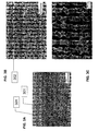
- Figures 3A and 3C show a typical example of the wire structure plated at a typical condition according to this example.
- Figure 3A shows the pattern before plating, a stack 10 nanometers silicon dioxide and then, 20 nanometers silicon nitride are deposited on the silicon. Vias of 200 nanometers diameter (301) are patterned with lithography and etching processes and the silicon substrate is exposed. The electroplated germanium nanowire structures (302) grow out of the pattern and maintain the diameter of the vias, 200 nm. (See figures 3B-3C ).
- Figure 4 is a wire structure grown at the same conditions as Figure 3 , but for a longer time. Micrometer-long wires are obtained with the shape still defmed by the pattern.
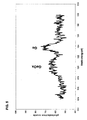
- Figure 5 shows the XPS analysis of a typical wire structure electroplated according to this example. Two peaks are denoted as elemental germanium and germanium oxide. The majority of the deposit is confirmed as germanium while the surface of the structure can be oxidized in the air.
- the electrolyte employed comprises a 0.5 mol/L solution of GeCl 4 in 1,3-propanediol. Both chemicals are highly pure and dry.
- the cathode is a patterned silicon having been pre-cleaned and patterned by standard microelectronics fabrication processes. A typical stack for patterning is prepared by depositing on silicon, about 10 nanometers thick of silicon dioxide and then, 20 nanometers thick silicon nitride. Features with 200 nanometers in dimension are patterned through silicon nitride and silicon dioxide with lithography and reactive ion etch processes. Immediately before the electroplating, the patterned silicon substrate is dipped in a 1:100 dilute HF for about 2 minutes to remove native oxide. InGa eutectic is applied on the backside of the silicon to form an ohmic contact, and the substrate is mounted on a rotating disk electrode.
- the electroplating is carried out in a galvanostatic mode and a current of about -4000mA/cm2 is typically used for producing the nanostructure.
- Figures 6A and 6B show typical structures plated at a typical conditions according to this example, on via and stripe patterns.
- Figure 6A shows that the electroplated germanium nanowire structures grow out of the via patterns and maintain the diameter of the vias, 200 nanometers.
- Figure 6B is a wall structure grown at the same conditions in this example, but on a stripe pattern. The wall structures grow out of the stripe patterns and maintain the shape of the stripes, hundreds of micrometers in length and 200 nanometers in width.
Landscapes
- Chemical & Material Sciences (AREA)
- Engineering & Computer Science (AREA)
- Materials Engineering (AREA)
- Organic Chemistry (AREA)
- Metallurgy (AREA)
- Chemical Kinetics & Catalysis (AREA)
- Electrochemistry (AREA)
- Nanotechnology (AREA)
- Crystallography & Structural Chemistry (AREA)
- Physics & Mathematics (AREA)
- Mathematical Physics (AREA)
- Theoretical Computer Science (AREA)
- Manufacturing & Machinery (AREA)
- Electroplating Methods And Accessories (AREA)
- Electrodes Of Semiconductors (AREA)
- Electroplating And Plating Baths Therefor (AREA)
Abstract
Description
- The field of the present disclosure relates to the nanostructure comprising germanium (Ge) nanowires. In particular, the present disclosure relates to electrodeposition of Ge onto patterned semiconductor substrates.
- Nanowire field effect transistors would allow 3-dimensional integration and thus a much higher device density than the current technologies. The key element of such a device is the semiconductor nanowire. So far, nanowires of a few semiconductor compounds produced by electroplating have been reported. However, nanowires of Si and Ge have only been produced by vacuum processes.
- Moreover the previously reported nanowire structures made from electroplating are produced with a template, which defines the shape of the structures. As illustrated in
Figures 1A and 1B , the template (100) with nanopores (101) has a layer of conductive material (102) at one side, which carries the electroplating current and wire structures (103) are electroplated with the shape defined by the pores. - Germanium is a semiconducting material with higher mobility as compared to silicon. There have been some limited suggestions of electrodeposition of germanium onto metals. However, they have not been especially successful. These efforts may have not been thwarted due to the high reversible potential of Ge and the very low hydrogen overpotential on Ge surfaces. Therefore, all of the plating current can result from the proton reduction (side reaction) and no Ge plating can occur once the electrode surface is covered by Ge. So far, three approaches of Ge electroplating have been reported.
- For instance, plating of germanium on metal substrates has been reported in alkaline aqueous solutions (see Fink et al., Journal of the Electrochemical Society, vol. 95, p. 80 (1948)) and in glycol solutions (see Szekely, Journal of the Electrochemical Society, vol. 98, p. 318 (1951) and
US patent 2,690,422 to Szekely ). More recently, some studies have been reported directed nucleation studies in ionic liquid media. See Endres, Electrochemical and Solid State Letters, vol. 5, p. C38 (2002); Endres, Physical Chemistry and Chemical Physics, vol. 4, p. 1640 (2002) and Endres, Physical Chemistry and Chemical Physics, vol. 4, p. 1649 (2002). - In the aqueous solution approach, an extremely alkaline solution (pH>13) was suggested to minimize the proton concentration and therefore suppress the reduction of proton. This approach is not compatible with most microelectronics processes due to the extremely high pH of the electrolyte, which cause damages to most of the structures that are built from dielectrics such as silicon oxides.
- In the non-aqueous solution approaches, where the glycol and ionic liquid solvents are used, the proton is either partially decreased or completely removed in the solution resulting in a much less side reaction. The techniques using ionic liquids suffer from the disadvantages of high viscosity and expenses.
- The present disclosure relates to a nanostructure that comprises a semiconductor substrate, and comprises Ge in contact with the substrate. The Ge is less than 1 micrometer in at least one dimension. In one embodiment the Ge extends outwardly from its substrate.
- The present disclosure also relates to a method as claimed in claim 1.
- The Ge is less than 1 micrometer in at least one dimension.. In one embodiment the Ge extends outwardly from its substrate and the Ge is less than 1 micrometer in diameter.
-
-
Figures 1A and 1B are schematic diagrams of prior art in electroplating metallic nanostructures. -
Figures 2A and 2B are schematic diagrams of prior art of a mushroom growth as is in most cases of electroplating through mask. -
Figure 2C is a schematic diagram of a nanostructure according to this invention. -
Figure 3A is an electron microscope photograph of a patterned semiconductor substrate prior to plating according to the present disclosure. -
Figures 3B and 3C are electron microscope photographs at different magnifications illustrating the germanium nanowires grown out of the patterned substrate ofFigure 3A . -
Figure 4 is an electron microscope photograph illustrating germanium wires grown out of a patterned semiconductor substrate. -
Figure 5 shows Ge XPS analysis of a germanium nanowire electroplated according to the present disclosure. The two peaks are denoted as elemented germanium and germanium oxide. -
Figures 6A and 6B are electron microscope photographs illustrating germanium wire- and wall-shaped structures grown out of a patterned semiconductor substrate. -
Figure 7 shows a schematic representation of an exemplary apparatus for electrodepositing Ge on semiconductor wafer substrates. - The present disclosure relates to providing germanium nanostructures on semiconductor substrates. Suitable semiconductor conductor substrates include but not limited to: Si-based and Ge-based semiconductors such as Si, Ge, SiGe alloys, SiC alloys, SiGeC alloys as well as III-V and II-VI semiconductors as well as any combinations of the above.
- According to the present disclosure germanium nanostructures are electroplated onto patterned semiconductor substrates having insulating regions and semiconductor regions. The insulating regions can be formed from dielectrics such as silicon oxides, silicon nitrides and aluminum oxide.
- The germanium can be electroplated directly onto the semiconductor substrate without any seed or intermediate layer such as a seed layer. If desired a seed layer such as copper or nickel layer can be deposited prior to the electroplating of the germanium. This seed layer can be formed prior to the fabrication of the dielectric stencil by standard deposition processes such as sputtering, evaporation, PVD and CVD. When present, the seed layer is typically about 10 to about 100 nanometers thick and more typically about 10 to about 20 nanometers thick. Other intermediate layer can also be deposited prior to the germanium plating by electrochemical deposition including electroless or electroplating techniques.
- The electroplating bath typically employed according to the present disclosure contains a source of germanium ions such as germanium tetrahalide and especially germanium tetrachloride and an organic solvent such as an alkyl diol. Examples of alkyl diols are alkyl diols typically having 2-5 carbon atoms and including ethylene glycol, propylene glycol, 1,3 propanediol, butylene glycol, 1,3 butanediol and pentylene glycol. The concentration of the source of germanium is typically about 0.2 to about 0.7 moles and more typically about 0.3 to about 0.5 moles/liter; an example being about 0.5 mol/L GeCl4. The components of the electroplating bath are desirably highly pure (>99.9%).
-
FIG. 7 shows aplating apparatus 10 that may be used to implement the Ge electroplating of the present disclosure.Apparatus 10 comprisesvessel 20 containingelectrolyte 30 andstationary anode 40.Substrate 50 is mounted on rotatingcathode 60 and immersed inelectrolyte 30. Rotatingcathode 60 and edges ofsubstrate 50 are protected from the electrolyte by insulatinghousing 70.Power supply 80 supplies a current betweenanode 40 and substrate/cathode 50/60. Atypical anode 40 is graphite. - The electrodeposition is typically carried out at temperature of about 50°C to about 90°C and more typically at about 70 to 80°C. The current density employed is typically about 2000 to about 8000 milliamps/cm2. Prior to immersing the semiconductor substrate into the plating bath, the substrate is typically cleaned, such as by washing with a dilute HF solution (1: 100). The plating both is typically aged such as for at least about 3 hours or in the alternative contains a small amount of water, e.g. about 0.5 g/L to about 2 g/L, a typical example being 1g/L.
- During plating the cathode rotates at a typical rate of about 500 rpm to about 2000 rpm with an example being about 1000 rpm. The electroplating is carried in a galvanostatic mode. The plating is carried out for sufficient time to provide germanium extending outwardly from the substrate typically to a length of about 0.1 µm to about 3 µm, more typically about 0.2 µm to about 1µm.
- As mentioned above, the present disclosure makes it possible to fabricate germanium nanowire structures without the use of template. The method of the present disclosure makes it possible to produce germanium nanowires by a self-constrained anistropic growth in the electroplating, completely different from a traditional template plating process. As illustrated in
Figures 2A, 2B and 2C , shallow patterns (200) with pores (201) are fabricated on a conductive or semi-conductive layer (202). Plating continues after the pores are filled. Instead of a mushroom cap (203) that occurs in most cases of electroplating, wire structures (204) are produced as they grow out of the pattern in an anisotropic manner maintaining the size defined by the pattern. - The following non-limiting examples are presented to further illustrate the present disclosure.
- The electrolyte employed comprises a 0.5 mol/L solution of GeCl4 in 1,3-propanediol. Both chemicals are highly pure and dry. The cathode is a patterned silicon having been pre-cleaned and patterned by standard microelectronics fabrication processes. A typical stack for patterning is prepared by depositing on silicon, about 10 nanometers thick of silicon dioxide and then, 20 nanometers thick silicon nitride. Features with 200 nanometers in dimension are patterned through silicon nitride and silicon dioxide with lithography and reactive ion etch processes. Immediately before the electroplating, the patterned silicon substrate is dipped in a 1:100 dilute HF for about 2 minutes to remove native oxide. InGa eutectic is applied on the backside of the silicon to form an ohmic contact, and the substrate is mounted on a rotating disk electrode as illustrated in
Figure 7 . - The fresh GeCl4 bath is aged by exposing to ambient conditions for at least 3 hours. The electrolyte is maintained at about 70-80°C. A graphite anode is used. The cathode rotates during plating at a typical rate of 1000 rpm. The electroplating is carried out in a galvanostatic mode and a current of about -4000mA/cm2 is typically used for producing the nanostructure.
-
Figures 3A and 3C show a typical example of the wire structure plated at a typical condition according to this example.Figure 3A shows the pattern before plating, astack 10 nanometers silicon dioxide and then, 20 nanometers silicon nitride are deposited on the silicon. Vias of 200 nanometers diameter (301) are patterned with lithography and etching processes and the silicon substrate is exposed. The electroplated germanium nanowire structures (302) grow out of the pattern and maintain the diameter of the vias, 200 nm. (Seefigures 3B-3C ).Figure 4 is a wire structure grown at the same conditions asFigure 3 , but for a longer time. Micrometer-long wires are obtained with the shape still defmed by the pattern. -
Figure 5 shows the XPS analysis of a typical wire structure electroplated according to this example. Two peaks are denoted as elemental germanium and germanium oxide. The majority of the deposit is confirmed as germanium while the surface of the structure can be oxidized in the air. - The electrolyte employed comprises a 0.5 mol/L solution of GeCl4 in 1,3-propanediol. Both chemicals are highly pure and dry. The cathode is a patterned silicon having been pre-cleaned and patterned by standard microelectronics fabrication processes. A typical stack for patterning is prepared by depositing on silicon, about 10 nanometers thick of silicon dioxide and then, 20 nanometers thick silicon nitride. Features with 200 nanometers in dimension are patterned through silicon nitride and silicon dioxide with lithography and reactive ion etch processes. Immediately before the electroplating, the patterned silicon substrate is dipped in a 1:100 dilute HF for about 2 minutes to remove native oxide. InGa eutectic is applied on the backside of the silicon to form an ohmic contact, and the substrate is mounted on a rotating disk electrode.
- About 1 g/L of water is added to the fresh GeCl4 bath. The electrolyte is maintained at about 70-80°C. A graphite anode is used. The cathode rotates during plating at a typical rate of 1000 rpm. The electroplating is carried out in a galvanostatic mode and a current of about -4000mA/cm2 is typically used for producing the nanostructure.
-
Figures 6A and 6B show typical structures plated at a typical conditions according to this example, on via and stripe patterns.Figure 6A shows that the electroplated germanium nanowire structures grow out of the via patterns and maintain the diameter of the vias, 200 nanometers.Figure 6B is a wall structure grown at the same conditions in this example, but on a stripe pattern. The wall structures grow out of the stripe patterns and maintain the shape of the stripes, hundreds of micrometers in length and 200 nanometers in width.
Claims (8)
- A method for forming a germanium-containing nanostructure comprising:forming amask on a semiconductor substrate, wherein said mask has at least one opening to expose said substrate;immersing said semiconductor substrate with said mask into a plating solution containing Ge;applying electric power between said semiconductor substrate and an anode in said plating solution whereby said semiconductor substrate where exposed is plated with germanium, which, as a result of the application of electric power, extends outwardly from said opening in contact with said substrate and any cross section of said germanium taken parallel with said substrate mimics the shape of said opening of the said mask.
- The method of Claim 1 wherein said semiconductor substrate is selected from the group consisting of Si, Ge, SiGe, SiC, GeC; SiGeC, III-V materials, and II-VI materials and mixtures thereof.
- The method of Claim 1 wherein said substrate is selected from the group consisting of Si, Ge and GaAs.
- The method of Claim 1 wherein said substrate contains dielectric regions.
- The method of Claim 1 wherein the plating bath contains an alkyl diol solvent.
- The method of Claim 5 wherein the alkyl diol solvent is selected from the group consisting of ethanediol, propanediol, butanediol and pentanediol.
- The method of Claim 6 wherein the alkyl diol is selected from the group consisting of ethylene glycol, propylene glycol and 1,3-propanediol.
- The method of Claim 4 wherein the source of germanium comprises GeCl4.
Applications Claiming Priority (2)
| Application Number | Priority Date | Filing Date | Title |
|---|---|---|---|
| US11/620,391 US7659200B2 (en) | 2007-01-05 | 2007-01-05 | Self-constrained anisotropic germanium nanostructure from electroplating |
| PCT/EP2007/064118 WO2008080828A1 (en) | 2007-01-05 | 2007-12-18 | Self-constrained anisotropic germanium nanostructure from electroplating |
Publications (2)
| Publication Number | Publication Date |
|---|---|
| EP2102900A1 EP2102900A1 (en) | 2009-09-23 |
| EP2102900B1 true EP2102900B1 (en) | 2012-05-30 |
Family
ID=39273301
Family Applications (1)
| Application Number | Title | Priority Date | Filing Date |
|---|---|---|---|
| EP07857746A Not-in-force EP2102900B1 (en) | 2007-01-05 | 2007-12-18 | Self-constrained anisotropic germanium nanostructure from electroplating |
Country Status (6)
| Country | Link |
|---|---|
| US (2) | US7659200B2 (en) |
| EP (1) | EP2102900B1 (en) |
| JP (1) | JP5137968B2 (en) |
| KR (1) | KR101174044B1 (en) |
| TW (1) | TWI409855B (en) |
| WO (1) | WO2008080828A1 (en) |
Cited By (1)
| Publication number | Priority date | Publication date | Assignee | Title |
|---|---|---|---|---|
| US20230223251A1 (en) * | 2020-04-28 | 2023-07-13 | Tokyo Electron Limited | Method of manufacturing semiconductor device, semiconductor manufacturing device, and system |
Families Citing this family (5)
| Publication number | Priority date | Publication date | Assignee | Title |
|---|---|---|---|---|
| JP4138407B2 (en) | 2002-08-30 | 2008-08-27 | 株式会社ニデック | Intraocular implant device |
| US9903033B2 (en) * | 2012-07-24 | 2018-02-27 | Uchicago Argonne Llc | Nanowire and microwire fabrication technique and product |
| US9263260B1 (en) * | 2014-12-16 | 2016-02-16 | International Business Machines Corporation | Nanowire field effect transistor with inner and outer gates |
| US9496263B1 (en) | 2015-10-23 | 2016-11-15 | International Business Machines Corporation | Stacked strained and strain-relaxed hexagonal nanowires |
| CN108315770B (en) * | 2018-02-07 | 2019-08-16 | 吉林师范大学 | A kind of germanium gallium nano wire and its growth in situ method |
Family Cites Families (19)
| Publication number | Priority date | Publication date | Assignee | Title |
|---|---|---|---|---|
| US2690422A (en) * | 1950-08-05 | 1954-09-28 | Sylvania Electric Prod | Electroplating of germanium |
| JPH02232935A (en) * | 1989-03-07 | 1990-09-14 | Matsushita Electric Ind Co Ltd | Thin film semiconductor element and manufacture thereof |
| US5270229A (en) * | 1989-03-07 | 1993-12-14 | Matsushita Electric Industrial Co., Ltd. | Thin film semiconductor device and process for producing thereof |
| CA2089791C (en) * | 1992-04-24 | 1998-11-24 | Michael J. Brady | Electronic devices having metallurgies containing copper-semiconductor compounds |
| DE19522054C1 (en) | 1995-06-17 | 1996-11-28 | Inst Halbleiterphysik Gmbh | Development of germanium quantum wires on silicon@ substrates |
| JPH10158883A (en) * | 1996-11-28 | 1998-06-16 | Nikon Corp | Method for manufacturing pattern-formed body |
| JPH11310776A (en) | 1998-04-30 | 1999-11-09 | Mitsubishi Materials Corp | Light-emitting material, method of manufacturing the same, and light-emitting element using the same |
| US6872645B2 (en) * | 2002-04-02 | 2005-03-29 | Nanosys, Inc. | Methods of positioning and/or orienting nanostructures |
| US6858521B2 (en) * | 2002-12-31 | 2005-02-22 | Samsung Electronics Co., Ltd. | Method for fabricating spaced-apart nanostructures |
| US20040144970A1 (en) * | 2002-10-07 | 2004-07-29 | Dunwei Wang | Nanowires |
| US7229498B2 (en) * | 2002-10-29 | 2007-06-12 | Midwest Research Institute | Nanostructures produced by phase-separation during growth of (III-V)1-x(IV2)x alloys |
| JP4016105B2 (en) * | 2003-03-26 | 2007-12-05 | 独立行政法人物質・材料研究機構 | Manufacturing method of silicon nanowires |
| US7545010B2 (en) * | 2003-08-08 | 2009-06-09 | Canon Kabushiki Kaisha | Catalytic sensor structure |
| JP4434658B2 (en) * | 2003-08-08 | 2010-03-17 | キヤノン株式会社 | Structure and manufacturing method thereof |
| WO2005064639A2 (en) * | 2003-12-22 | 2005-07-14 | Koninklijke Philips Electronics N.V. | Fabricating a set of semiconducting nanowires, and electric device comprising a set of nanowires |
| KR100658905B1 (en) * | 2004-04-29 | 2006-12-15 | 한국표준과학연구원 | Semiconductor Nanostructures and Formation Methods |
| GB0416600D0 (en) * | 2004-07-24 | 2004-08-25 | Univ Newcastle | A process for manufacturing micro- and nano-devices |
| US7158219B2 (en) * | 2004-09-16 | 2007-01-02 | Hewlett-Packard Development Company, L.P. | SERS-active structures including nanowires |
| FR2885913B1 (en) * | 2005-05-18 | 2007-08-10 | Centre Nat Rech Scient | COMPOSITE ELEMENT COMPRISING A CONDUCTIVE SUBSTRATE AND A NANOSTRUCTURED METAL COATING. |
-
2007
- 2007-01-05 US US11/620,391 patent/US7659200B2/en not_active Expired - Fee Related
- 2007-12-18 JP JP2009544382A patent/JP5137968B2/en not_active Expired - Fee Related
- 2007-12-18 EP EP07857746A patent/EP2102900B1/en not_active Not-in-force
- 2007-12-18 WO PCT/EP2007/064118 patent/WO2008080828A1/en not_active Ceased
- 2007-12-18 KR KR1020097010647A patent/KR101174044B1/en not_active Expired - Fee Related
-
2008
- 2008-01-02 TW TW097100120A patent/TWI409855B/en not_active IP Right Cessation
-
2009
- 2009-08-14 US US12/541,559 patent/US8115191B2/en not_active Expired - Fee Related
Cited By (1)
| Publication number | Priority date | Publication date | Assignee | Title |
|---|---|---|---|---|
| US20230223251A1 (en) * | 2020-04-28 | 2023-07-13 | Tokyo Electron Limited | Method of manufacturing semiconductor device, semiconductor manufacturing device, and system |
Also Published As
| Publication number | Publication date |
|---|---|
| EP2102900A1 (en) | 2009-09-23 |
| TW200839850A (en) | 2008-10-01 |
| JP2010514944A (en) | 2010-05-06 |
| KR20090095569A (en) | 2009-09-09 |
| US8115191B2 (en) | 2012-02-14 |
| US7659200B2 (en) | 2010-02-09 |
| JP5137968B2 (en) | 2013-02-06 |
| TWI409855B (en) | 2013-09-21 |
| US20080166858A1 (en) | 2008-07-10 |
| US20090302305A1 (en) | 2009-12-10 |
| WO2008080828A1 (en) | 2008-07-10 |
| KR101174044B1 (en) | 2012-08-16 |
Similar Documents
| Publication | Publication Date | Title |
|---|---|---|
| JP5270639B2 (en) | Single crystal substrate | |
| US7718531B2 (en) | Method for forming catalyst nanoparticles for growing elongated nanostructures | |
| Peng et al. | Motility of metal nanoparticles in silicon and induced anisotropic silicon etching | |
| US8115191B2 (en) | Self-constrained anisotropic germanium nanostructure from electroplating | |
| CN101796648A (en) | Method for reusing wafer for growing vertically aligned wire arrays | |
| CN1236984A (en) | Process for forming fine wiring | |
| Ivanova et al. | Electrochemical deposition of Ni and Cu onto monocrystalline n-Si (100) wafers and into nanopores in Si/SiO2 template | |
| Fukami et al. | Electrodeposition of noble metals into ordered macropores in p-type silicon | |
| US7918984B2 (en) | Method of electrodepositing germanium compound materials on a substrate | |
| Jung et al. | Fabrication and characterization of porous silicon nanowires | |
| US10037896B2 (en) | Electro-assisted transfer and fabrication of wire arrays | |
| JP2004526304A (en) | Electrochemical method for polishing copper films on semiconductor substrates | |
| TW200845218A (en) | Structures containing electrodeposited germanium and methods for their fabrication | |
| Yao et al. | Atomically resolved scanning tunneling microscopy images of InP (001),(111) A, and (111) B surfaces in sulfuric acid solution | |
| Tokuda et al. | Selective growth of Cu nanowires on Si (111) substrates | |
| Lublow et al. | Fractal photocorrosion of silicon electrodes in concentrated ammonium fluoride | |
| CN110911555B (en) | Deep hole superlattice filling method based on electrochemical deposition | |
| Huang et al. | Anisotropic growth of nanostructures in germanium electroplating | |
| McSweeney et al. | Fabrication and characterization of single-crystal metal-assisted chemically etched rough Si nanowires for lithium-ion battery anodes | |
| KR101292863B1 (en) | Epitaxial growth and single crystal thin film fabrication using electrodeposition | |
| Tong et al. | Study of the electroless silver seed formation on silicon surface | |
| CN109244053A (en) | A kind of composite construction and its manufacturing method improving the thermomechanical reliability of TSV | |
| RU2778998C1 (en) | METHOD FOR FORMING A LAYER OF GOLD ELECTROCHEMICALLY DEPOSITED FROM ELECTROLYTES WITH pH = 6-7 ON THE SURFACE OF SILICON SEMICONDUCTOR STRUCTURES | |
| TWI569391B (en) | Circuit structure and method of fabricating the same | |
| Chuang et al. | Through-silicon via arrays manufactured by photo assisted electrochemical etching and copper electroplating under SC-CO 2 environment |
Legal Events
| Date | Code | Title | Description |
|---|---|---|---|
| PUAI | Public reference made under article 153(3) epc to a published international application that has entered the european phase |
Free format text: ORIGINAL CODE: 0009012 |
|
| 17P | Request for examination filed |
Effective date: 20090710 |
|
| AK | Designated contracting states |
Kind code of ref document: A1 Designated state(s): AT BE BG CH CY CZ DE DK EE ES FI FR GB GR HU IE IS IT LI LT LU LV MC MT NL PL PT RO SE SI SK TR |
|
| RIN1 | Information on inventor provided before grant (corrected) |
Inventor name: HUANG, QIANG Inventor name: COHEN, GUY Inventor name: DELIGIANNI, HARIKLIA Inventor name: ROMANKIW, LUBOMYR |
|
| DAX | Request for extension of the european patent (deleted) | ||
| REG | Reference to a national code |
Ref country code: DE Ref legal event code: R079 Ref document number: 602007023068 Country of ref document: DE Free format text: PREVIOUS MAIN CLASS: H01L0021208000 Ipc: H01L0021020000 |
|
| GRAP | Despatch of communication of intention to grant a patent |
Free format text: ORIGINAL CODE: EPIDOSNIGR1 |
|
| RIC1 | Information provided on ipc code assigned before grant |
Ipc: C25D 7/12 20060101ALI20120105BHEP Ipc: C25D 5/02 20060101ALI20120105BHEP Ipc: B82Y 10/00 20110101ALI20120105BHEP Ipc: C25D 3/54 20060101ALI20120105BHEP Ipc: H01L 21/02 20060101AFI20120105BHEP Ipc: H01L 21/208 20060101ALI20120105BHEP |
|
| GRAS | Grant fee paid |
Free format text: ORIGINAL CODE: EPIDOSNIGR3 |
|
| GRAA | (expected) grant |
Free format text: ORIGINAL CODE: 0009210 |
|
| AK | Designated contracting states |
Kind code of ref document: B1 Designated state(s): AT BE BG CH CY CZ DE DK EE ES FI FR GB GR HU IE IS IT LI LT LU LV MC MT NL PL PT RO SE SI SK TR |
|
| REG | Reference to a national code |
Ref country code: GB Ref legal event code: FG4D |
|
| REG | Reference to a national code |
Ref country code: CH Ref legal event code: EP |
|
| REG | Reference to a national code |
Ref country code: AT Ref legal event code: REF Ref document number: 560407 Country of ref document: AT Kind code of ref document: T Effective date: 20120615 Ref country code: CH Ref legal event code: NV Representative=s name: IBM RESEARCH GMBH ZURICH RESEARCH LABORATORY INTEL |
|
| REG | Reference to a national code |
Ref country code: IE Ref legal event code: FG4D |
|
| REG | Reference to a national code |
Ref country code: GB Ref legal event code: 746 Effective date: 20120702 |
|
| REG | Reference to a national code |
Ref country code: DE Ref legal event code: R096 Ref document number: 602007023068 Country of ref document: DE Effective date: 20120726 |
|
| REG | Reference to a national code |
Ref country code: DE Ref legal event code: R084 Ref document number: 602007023068 Country of ref document: DE Effective date: 20120606 |
|
| REG | Reference to a national code |
Ref country code: NL Ref legal event code: VDEP Effective date: 20120530 |
|
| REG | Reference to a national code |
Ref country code: LT Ref legal event code: MG4D Effective date: 20120530 |
|
| PG25 | Lapsed in a contracting state [announced via postgrant information from national office to epo] |
Ref country code: FI Free format text: LAPSE BECAUSE OF FAILURE TO SUBMIT A TRANSLATION OF THE DESCRIPTION OR TO PAY THE FEE WITHIN THE PRESCRIBED TIME-LIMIT Effective date: 20120530 Ref country code: LT Free format text: LAPSE BECAUSE OF FAILURE TO SUBMIT A TRANSLATION OF THE DESCRIPTION OR TO PAY THE FEE WITHIN THE PRESCRIBED TIME-LIMIT Effective date: 20120530 Ref country code: CY Free format text: LAPSE BECAUSE OF FAILURE TO SUBMIT A TRANSLATION OF THE DESCRIPTION OR TO PAY THE FEE WITHIN THE PRESCRIBED TIME-LIMIT Effective date: 20120530 Ref country code: IS Free format text: LAPSE BECAUSE OF FAILURE TO SUBMIT A TRANSLATION OF THE DESCRIPTION OR TO PAY THE FEE WITHIN THE PRESCRIBED TIME-LIMIT Effective date: 20120930 Ref country code: SE Free format text: LAPSE BECAUSE OF FAILURE TO SUBMIT A TRANSLATION OF THE DESCRIPTION OR TO PAY THE FEE WITHIN THE PRESCRIBED TIME-LIMIT Effective date: 20120530 |
|
| REG | Reference to a national code |
Ref country code: AT Ref legal event code: MK05 Ref document number: 560407 Country of ref document: AT Kind code of ref document: T Effective date: 20120530 |
|
| PG25 | Lapsed in a contracting state [announced via postgrant information from national office to epo] |
Ref country code: SI Free format text: LAPSE BECAUSE OF FAILURE TO SUBMIT A TRANSLATION OF THE DESCRIPTION OR TO PAY THE FEE WITHIN THE PRESCRIBED TIME-LIMIT Effective date: 20120530 Ref country code: LV Free format text: LAPSE BECAUSE OF FAILURE TO SUBMIT A TRANSLATION OF THE DESCRIPTION OR TO PAY THE FEE WITHIN THE PRESCRIBED TIME-LIMIT Effective date: 20120530 Ref country code: GR Free format text: LAPSE BECAUSE OF FAILURE TO SUBMIT A TRANSLATION OF THE DESCRIPTION OR TO PAY THE FEE WITHIN THE PRESCRIBED TIME-LIMIT Effective date: 20120831 |
|
| PG25 | Lapsed in a contracting state [announced via postgrant information from national office to epo] |
Ref country code: BE Free format text: LAPSE BECAUSE OF FAILURE TO SUBMIT A TRANSLATION OF THE DESCRIPTION OR TO PAY THE FEE WITHIN THE PRESCRIBED TIME-LIMIT Effective date: 20120530 |
|
| PG25 | Lapsed in a contracting state [announced via postgrant information from national office to epo] |
Ref country code: RO Free format text: LAPSE BECAUSE OF FAILURE TO SUBMIT A TRANSLATION OF THE DESCRIPTION OR TO PAY THE FEE WITHIN THE PRESCRIBED TIME-LIMIT Effective date: 20120530 Ref country code: AT Free format text: LAPSE BECAUSE OF FAILURE TO SUBMIT A TRANSLATION OF THE DESCRIPTION OR TO PAY THE FEE WITHIN THE PRESCRIBED TIME-LIMIT Effective date: 20120530 Ref country code: CZ Free format text: LAPSE BECAUSE OF FAILURE TO SUBMIT A TRANSLATION OF THE DESCRIPTION OR TO PAY THE FEE WITHIN THE PRESCRIBED TIME-LIMIT Effective date: 20120530 Ref country code: DK Free format text: LAPSE BECAUSE OF FAILURE TO SUBMIT A TRANSLATION OF THE DESCRIPTION OR TO PAY THE FEE WITHIN THE PRESCRIBED TIME-LIMIT Effective date: 20120530 Ref country code: EE Free format text: LAPSE BECAUSE OF FAILURE TO SUBMIT A TRANSLATION OF THE DESCRIPTION OR TO PAY THE FEE WITHIN THE PRESCRIBED TIME-LIMIT Effective date: 20120530 Ref country code: NL Free format text: LAPSE BECAUSE OF FAILURE TO SUBMIT A TRANSLATION OF THE DESCRIPTION OR TO PAY THE FEE WITHIN THE PRESCRIBED TIME-LIMIT Effective date: 20120530 Ref country code: SK Free format text: LAPSE BECAUSE OF FAILURE TO SUBMIT A TRANSLATION OF THE DESCRIPTION OR TO PAY THE FEE WITHIN THE PRESCRIBED TIME-LIMIT Effective date: 20120530 |
|
| PG25 | Lapsed in a contracting state [announced via postgrant information from national office to epo] |
Ref country code: PT Free format text: LAPSE BECAUSE OF FAILURE TO SUBMIT A TRANSLATION OF THE DESCRIPTION OR TO PAY THE FEE WITHIN THE PRESCRIBED TIME-LIMIT Effective date: 20121001 Ref country code: PL Free format text: LAPSE BECAUSE OF FAILURE TO SUBMIT A TRANSLATION OF THE DESCRIPTION OR TO PAY THE FEE WITHIN THE PRESCRIBED TIME-LIMIT Effective date: 20120530 Ref country code: IT Free format text: LAPSE BECAUSE OF FAILURE TO SUBMIT A TRANSLATION OF THE DESCRIPTION OR TO PAY THE FEE WITHIN THE PRESCRIBED TIME-LIMIT Effective date: 20120530 |
|
| PLBE | No opposition filed within time limit |
Free format text: ORIGINAL CODE: 0009261 |
|
| STAA | Information on the status of an ep patent application or granted ep patent |
Free format text: STATUS: NO OPPOSITION FILED WITHIN TIME LIMIT |
|
| PG25 | Lapsed in a contracting state [announced via postgrant information from national office to epo] |
Ref country code: ES Free format text: LAPSE BECAUSE OF FAILURE TO SUBMIT A TRANSLATION OF THE DESCRIPTION OR TO PAY THE FEE WITHIN THE PRESCRIBED TIME-LIMIT Effective date: 20120910 |
|
| 26N | No opposition filed |
Effective date: 20130301 |
|
| REG | Reference to a national code |
Ref country code: DE Ref legal event code: R097 Ref document number: 602007023068 Country of ref document: DE Effective date: 20130301 |
|
| PG25 | Lapsed in a contracting state [announced via postgrant information from national office to epo] |
Ref country code: BG Free format text: LAPSE BECAUSE OF FAILURE TO SUBMIT A TRANSLATION OF THE DESCRIPTION OR TO PAY THE FEE WITHIN THE PRESCRIBED TIME-LIMIT Effective date: 20120830 Ref country code: MC Free format text: LAPSE BECAUSE OF NON-PAYMENT OF DUE FEES Effective date: 20121231 |
|
| REG | Reference to a national code |
Ref country code: CH Ref legal event code: PL |
|
| REG | Reference to a national code |
Ref country code: IE Ref legal event code: MM4A |
|
| REG | Reference to a national code |
Ref country code: FR Ref legal event code: ST Effective date: 20130830 |
|
| PG25 | Lapsed in a contracting state [announced via postgrant information from national office to epo] |
Ref country code: CH Free format text: LAPSE BECAUSE OF NON-PAYMENT OF DUE FEES Effective date: 20121231 Ref country code: LI Free format text: LAPSE BECAUSE OF NON-PAYMENT OF DUE FEES Effective date: 20121231 Ref country code: IE Free format text: LAPSE BECAUSE OF NON-PAYMENT OF DUE FEES Effective date: 20121218 |
|
| PG25 | Lapsed in a contracting state [announced via postgrant information from national office to epo] |
Ref country code: FR Free format text: LAPSE BECAUSE OF NON-PAYMENT OF DUE FEES Effective date: 20130102 Ref country code: MT Free format text: LAPSE BECAUSE OF FAILURE TO SUBMIT A TRANSLATION OF THE DESCRIPTION OR TO PAY THE FEE WITHIN THE PRESCRIBED TIME-LIMIT Effective date: 20120530 |
|
| PG25 | Lapsed in a contracting state [announced via postgrant information from national office to epo] |
Ref country code: TR Free format text: LAPSE BECAUSE OF FAILURE TO SUBMIT A TRANSLATION OF THE DESCRIPTION OR TO PAY THE FEE WITHIN THE PRESCRIBED TIME-LIMIT Effective date: 20120530 |
|
| PG25 | Lapsed in a contracting state [announced via postgrant information from national office to epo] |
Ref country code: LU Free format text: LAPSE BECAUSE OF NON-PAYMENT OF DUE FEES Effective date: 20121218 |
|
| PG25 | Lapsed in a contracting state [announced via postgrant information from national office to epo] |
Ref country code: HU Free format text: LAPSE BECAUSE OF FAILURE TO SUBMIT A TRANSLATION OF THE DESCRIPTION OR TO PAY THE FEE WITHIN THE PRESCRIBED TIME-LIMIT Effective date: 20071218 |
|
| PGFP | Annual fee paid to national office [announced via postgrant information from national office to epo] |
Ref country code: GB Payment date: 20151216 Year of fee payment: 9 |
|
| REG | Reference to a national code |
Ref country code: DE Ref legal event code: R082 Ref document number: 602007023068 Country of ref document: DE Representative=s name: RICHARDT PATENTANWAELTE PARTG MBB, DE Ref country code: DE Ref legal event code: R081 Ref document number: 602007023068 Country of ref document: DE Owner name: GLOBALFOUNDRIES INC., KY Free format text: FORMER OWNER: INTERNATIONAL BUSINESS MACHINES CORPORATION, ARMONK, N.Y., US |
|
| REG | Reference to a national code |
Ref country code: DE Ref legal event code: R082 Ref document number: 602007023068 Country of ref document: DE Representative=s name: RICHARDT PATENTANWAELTE PARTG MBB, DE Ref country code: DE Ref legal event code: R081 Ref document number: 602007023068 Country of ref document: DE Owner name: GLOBALFOUNDRIES INC., KY Free format text: FORMER OWNER: GLOBALFOUNDRIES US 2 LLC (N.D.GES.DES STAATES DELAWARE), HOPEWELL JUNCTION, N.Y., US |
|
| PGFP | Annual fee paid to national office [announced via postgrant information from national office to epo] |
Ref country code: DE Payment date: 20161213 Year of fee payment: 10 |
|
| GBPC | Gb: european patent ceased through non-payment of renewal fee |
Effective date: 20161218 |
|
| PG25 | Lapsed in a contracting state [announced via postgrant information from national office to epo] |
Ref country code: GB Free format text: LAPSE BECAUSE OF NON-PAYMENT OF DUE FEES Effective date: 20161218 |
|
| REG | Reference to a national code |
Ref country code: DE Ref legal event code: R119 Ref document number: 602007023068 Country of ref document: DE |
|
| PG25 | Lapsed in a contracting state [announced via postgrant information from national office to epo] |
Ref country code: DE Free format text: LAPSE BECAUSE OF NON-PAYMENT OF DUE FEES Effective date: 20180703 |