EP2101554B1 - Casing with circuit board - Google Patents
Casing with circuit board Download PDFInfo
- Publication number
- EP2101554B1 EP2101554B1 EP20090405030 EP09405030A EP2101554B1 EP 2101554 B1 EP2101554 B1 EP 2101554B1 EP 20090405030 EP20090405030 EP 20090405030 EP 09405030 A EP09405030 A EP 09405030A EP 2101554 B1 EP2101554 B1 EP 2101554B1
- Authority
- EP
- European Patent Office
- Prior art keywords
- circuit board
- printed circuit
- housing
- connecting ring
- partition wall
- Prior art date
- Legal status (The legal status is an assumption and is not a legal conclusion. Google has not performed a legal analysis and makes no representation as to the accuracy of the status listed.)
- Expired - Fee Related
Links
Images


Classifications
-
- H—ELECTRICITY
- H05—ELECTRIC TECHNIQUES NOT OTHERWISE PROVIDED FOR
- H05K—PRINTED CIRCUITS; CASINGS OR CONSTRUCTIONAL DETAILS OF ELECTRIC APPARATUS; MANUFACTURE OF ASSEMBLAGES OF ELECTRICAL COMPONENTS
- H05K7/00—Constructional details common to different types of electric apparatus
- H05K7/14—Mounting supporting structure in casing or on frame or rack
- H05K7/1417—Mounting supporting structure in casing or on frame or rack having securing means for mounting boards, plates or wiring boards
- H05K7/142—Spacers not being card guides
-
- H—ELECTRICITY
- H05—ELECTRIC TECHNIQUES NOT OTHERWISE PROVIDED FOR
- H05K—PRINTED CIRCUITS; CASINGS OR CONSTRUCTIONAL DETAILS OF ELECTRIC APPARATUS; MANUFACTURE OF ASSEMBLAGES OF ELECTRICAL COMPONENTS
- H05K7/00—Constructional details common to different types of electric apparatus
- H05K7/14—Mounting supporting structure in casing or on frame or rack
- H05K7/1417—Mounting supporting structure in casing or on frame or rack having securing means for mounting boards, plates or wiring boards
Description
Die Erfindung betrifft eine Vorrichtung, umfassend eine in einem Gehäuse angeordnete Leiterplatine für eine elektrische und/oder elektronische Schaltung, wobei die Leiterplatine einen vorderen Bereich und einen hinteren Bereich aufweist. Des Weiteren ist ein Verfahren zur Herstellung eines Gehäuses mit einer Leiterplatine Gegenstand der Erfindung.The invention relates to a device comprising a printed circuit board arranged in a housing for an electrical and / or electronic circuit, wherein the printed circuit board has a front region and a rear region. Furthermore, a method for producing a housing with a printed circuit board is the subject of the invention.
Leiterplatinen für elektronische Schaltungen von elektrischen oder elektronischen Geräten werden üblicherweise in einem Gehäuse angeordnet, um sie vor Verschmutzung und mechanischen Einwirkungen zu schützen. Zudem stellen die Gehäuse auch einen Schutz für den Benutzer dar, da diese sicherstellen, dass der Benutzer nicht mit den teilweise hohen Spannungen auf der Leiterplatine in Berührung kommen kann.Circuit boards for electronic circuits of electrical or electronic devices are usually placed in a housing to protect them from contamination and mechanical effects. In addition, the housing also provide protection for the user, as they ensure that the user can not come into contact with the sometimes high voltages on the printed circuit board.
Gehäuse für Leiterplatinen sind zwar in den verschiedensten Ausformungen bereits kommerziell erhältlich. Die meisten Gehäuse sind aber für den Innenbereich konzipiert und weisen lediglich eine beschränkte mechanische Festigkeit auf. Speziell robuste Gehäuse existieren zwar ebenfalls, diese sind aber meist sehr klobig und entsprechend unhandlich. Zudem sind die speziell robusten Gehäuse relativ kompliziert im Aufbau und der Herstellung und dementsprechend teuer.Although housings for printed circuit boards are already commercially available in a wide variety of designs. However, most cases are designed for indoor use and have only limited mechanical strength. Although particularly robust housings also exist, these are usually very clumsy and accordingly unwieldy. In addition, the specially robust housing are relatively complicated in construction and production and therefore expensive.
Insbesondere im militärischen Umfeld werden elektrische oder elektronische Geräte im Innen- und im Aussenbereich stark beansprucht. Da die Geräte innert kurzer Zeit mehrmals an neue Standorte transportiert und neu verkabelt werden müssen, werden die Gehäuse derartiger Geräte mechanisch stark gefordert. Aufgrund der mobilen Verwendung der Geräte, sind diese z. B. beim Transport immer wieder starken Erschütterungen ausgesetzt und das ständige Ein- und Ausstecken von Steckern in den Steckerbuchsen der Geräte ist ebenfalls belastend. Hierbei sind insbesondere die relativ dünnen Leiterplatinen gefährdet. Werden die Leiterplatinen mehrmals grossen mechanischen Belastungen ausgesetzt, kann es vorkommen, dass z. B. Leiterbahnen brechen und das Gerät dadurch unbrauchbar wird. Im Aussenbereich werden an die Gehäuse nochmals erhöhte Anforderungen gestellt, da diese z. B. zusätzlichen Schutz vor Feuchtigkeit, Wasser, Hitze oder Staub bieten müssen. Um den Transportaufwand möglichst gering zu halten, ist es wünschenswert, dass die Geräte möglichst leichte und kompakte Gehäuse aufweisen, welche zudem bezüglich Robustheit befriedigen.Especially in the military environment electrical or electronic devices are heavily used indoors and outdoors. Since the devices have to be transported to new locations and rewired several times within a short time, the housings of such devices are mechanically challenged. Due to the mobile use of the devices, these are z. B. repeatedly exposed during transport strong shocks and the constant plugging and unplugging of plugs in the sockets of the devices is also onerous. Here, in particular, the relatively thin printed circuit boards are at risk. If the circuit boards are exposed to large mechanical loads several times, it can happen that, for. B. break tracks and the device is unusable. In the outdoor area of the housing again increased demands are made, as these z. B. must provide additional protection against moisture, water, heat or dust. In order to keep the transport costs as low as possible, it is desirable that the devices have the lightest and most compact housing, which also satisfy with respect to robustness.
Es besteht daher nach wie vor Bedarf nach Gehäusen für Leiterplatinen, welche gleichzeitig robust, gut handhabbar und kostengünstig in der Herstellung sind.There is therefore still a need for housings for printed circuit boards, which are robust, easy to handle and inexpensive to manufacture at the same time.
Die
Die
Die
Die
Aufgabe der Erfindung ist es, eine dem eingangs genannten technischen Gebiet zugehörende verbesserte Vorrichtung zu schaffen, welche einfach herstellbar und robust ist.The object of the invention is to provide an improved device belonging to the technical field mentioned at the beginning which is easy to manufacture and robust.
Die Lösung der Aufgabe ist durch die Merkmale des Anspruchs 1 definiert. Gemäss der Erfindung ist die Leiterplatine zwischen dem vorderen Bereich und dem hinteren Bereich mechanisch im Gehäuse abgestützt, wobei ein Innenraum des Gehäuses durch eine Trennwand in zwei Teilräume separiert ist und die Leiterplatine durch einen in der Trennwand eingebrachten Schlitz hindurch ragt.The solution of the problem is defined by the features of claim 1. According to the invention, the printed circuit board between the front portion and the rear portion is mechanically supported in the housing, wherein an interior of the housing is separated by a partition wall into two subspaces and the printed circuit board protrudes through an inserted in the partition slot.
Durch die Abstützung der Leiterplatine zwischen den Endbereichen wird insbesondere erreicht, dass die Leiterplatine bei starker mechanischer Einwirkung, wie z. B. Erschütterungen oder Schlägen, welche zu entsprechend hohen Beschleunigungskräften auf das Gehäuse führen, nicht übermässig durchgebogen wird. Damit wird bestmöglich verhindert, dass durch die beim Durchbiegen auftretenden Kräfte Verbindungsleitungen auf der Leiterplatine beschädigen oder dass Bauelemente auf der Leiterplatine aus ihren Lötstellen gerissen werden oder gar zerbrechen.Due to the support of the printed circuit board between the end regions is achieved in particular that the printed circuit board with strong mechanical action, such. B. shocks or blows, which lead to correspondingly high acceleration forces on the housing, is not overly bent. This optimally prevents the forces occurring during bending from damaging connecting lines on the printed circuit board or causing components on the printed circuit board to be torn from their solder joints or even to break.
Damit ist es möglich, handelsübliche Leiterplatinen im Gehäuse unterzubringen und dennoch eine robuste Vorrichtung zu erhalten. Dadurch wird auch die Herstellung der erfindungsgemässen Vorrichtung bzw. eines darauf basierenden Geräts vereinfacht, da keine speziell robusten oder stabilen Leiterplatinen gefertigt werden müssen, sondern auf bekannte Leiterplatinen zurückgegriffen werden kann.This makes it possible to accommodate commercially available printed circuit boards in the housing and still obtain a robust device. This also simplifies the production of the device according to the invention or of a device based thereon, since no particularly robust or stable printed circuit boards have to be manufactured, but recourse can be had to known printed circuit boards.
Ein Gerät, basierend auf dem erfindungsgemässen Gehäuse mit Leiterplatine, ist daher bestens geeignet für anspruchvolle Anwendungen, beispielsweise im militärischen Umfeld, in Katastrophengebieten oder bei Expeditionen.A device based on the inventive housing with printed circuit board, therefore, is ideally suited for demanding applications, such as military environment, disaster areas or expeditions.
Ein Innenraum des Gehäuses ist erfindungsgemäss durch eine Trennwand in zwei Teilräume separiert, wobei die Leiterplatine durch einen in der Trennwand eingebrachten Schlitz hindurch ragt und durch die Trennwand abgestützt ist. Damit wird eine besonders einfache Abstützung möglich, da die Leiterplatine lediglich im Schlitz platziert werden muss und die erfindungsgemässe Abstützung durch die Trennwand erfolgt. Eine aufwändige Montage von Haltevorrichtungen, wie z. B. Schrauben oder Klammern, zur Abstützung im Gehäuse kann so vermieden werden. Es ist aber grundsätzlich auch möglich, die Leiterplatine mit an sich bekannten Haltevorrichtungen, beispielsweise Schrauben, Haltestiften oder Klammern, im Gehäuse abzustützen.An interior of the housing is separated according to the invention by a partition wall into two subspaces, wherein the printed circuit board protrudes through a slot introduced in the partition and is supported by the partition wall. This will be a special simple support possible because the circuit board must be placed only in the slot and the inventive support is carried out through the partition. An elaborate assembly of holding devices, such. As screws or brackets, for support in the housing can be avoided. However, it is also possible in principle to support the printed circuit board with known holding devices, for example screws, holding pins or clamps, in the housing.
Besonders bevorzugt bestehen abgesehen vom Schlitz im Wesentlichen keine weiteren Verbindungen zwischen den beiden Teilräumen des Gehäuses bzw. die Trennwand ist so ausgebildet, dass diese die beiden Teilräume bis auf den Schlitz vollständig voneinander abtrennt. Damit wird unter Anderem die Festigkeit bzw. Robustheit des Gehäuses bestmöglich verbessert, da die Trennwand eine zusätzliche Funktion als Stützelement für das Gehäuse selbst erfüllt. Es ist aber grundsätzlich auch möglich, eine Trennwand vorzusehen, welche die beiden Teilräume des Gehäuses nicht vollständig voneinander abtrennt. In diesem Fall ist aber die Funktion als Stützelement entsprechend reduziert.Apart from the slot, there are essentially no further connections between the two subspaces of the housing, or the partition wall is designed in such a way that it completely separates the two subspaces apart from the slot. Thus, inter alia, the strength and robustness of the housing is optimally improved, since the partition fulfills an additional function as a support element for the housing itself. But it is in principle also possible to provide a partition which does not completely separate the two subspaces of the housing from each other. In this case, however, the function is correspondingly reduced as a support element.
Der Schlitz in der Trennwand ist insbesondere derart dimensioniert, dass dieser von einem im Schlitz vorliegenden Bereich der Leiterplatine vollständig ausgefüllt ist. Dadurch wird eine bestmögliche Abstützung der Leiterplatine durch die Trennwand erzielt, da die Leiterplatine wenigstens mit der oberen und der unteren Seite direkt an der Trennwand anliegt, was einer Durchbiegung in idealer Weise entgegenwirkt. Zudem wird die Leiterplatine so entlang einer gesamten Breite flächig abgestützt. Diese flächige Abstützung reduziert insbesondere die bei einer Abstützung durch bekannte Vorrichtungen, wie z. B. Schrauben oder Haltestifte, auftretenden punktuellen Drücke, welche bei mechanischen Einwirkungen auf die Leiterplatine entstehen. Prinzipiell kann der Schlitz aber auch grösser dimensioniert sein, so dass er von der Leiterplatine nicht vollständig ausgefüllt wird.The slot in the partition is in particular dimensioned such that it is completely filled by a present in the slot area of the printed circuit board. As a result, the best possible support of the printed circuit board is achieved by the partition wall, since the printed circuit board rests at least with the upper and the lower side directly to the partition wall, which counteracts a deflection in an ideal manner. In addition, the printed circuit board is supported flat along an entire width. This planar support reduces in particular the case of a support by known devices, such. As screws or retaining pins, occurring punctual pressures, which arise in mechanical effects on the circuit board. In principle, however, the slot can also be dimensioned larger, so that it is not completely filled by the printed circuit board.
Liegt eine Trennwand im Gehäuse vor, so ist die Leiterplatine bevorzugt senkrecht zur Trennwand angeordnet. Da bei einer mechanischen Einwirkung auf das Gehäuse mit Leiterplatine insbesondere die Durchbiegung in einer Richtung senkrecht zur Ober- bzw. Unterseite der Leiterplatine verhindert werden soll, hat sich gezeigt, dass eine senkrecht zur Leiterplatine bzw. deren Ober- oder Unterseite angeordnete Trennwand eine bestmögliche Abstützung ermöglicht. Die Trennwand kann somit verhältnismässig dünn ausgebildet sein und dennoch eine ausreichende Stabilität bzw. Abstützung gewährleisten, da die auftretenden Kräfte hauptsächlich parallel zur Ebene der Trennwand wirken. Aus analogen Gründen steht die Trennwand mit Vorteil auch senkrecht zu einer inneren Seitenfläche des Gehäuses.If there is a partition in the housing, the printed circuit board is preferably arranged perpendicular to the partition. Since in a mechanical action on the housing with printed circuit board in particular the deflection in a direction perpendicular to the top or bottom of the printed circuit board to be prevented, it has been shown that a perpendicular to the printed circuit board or its top or bottom partition arranged a best possible support allows. The partition can thus be made relatively thin and yet ensure sufficient stability or support, because the forces acting mainly parallel to the plane of the partition. For analog reasons, the partition wall is advantageously also perpendicular to an inner side surface of the housing.
Es ist jedoch auch möglich, eine Trennwand vorzusehen, welche nicht senkrecht zur Leiterplatine angeordnet ist. Dies bringt aber unter Umständen den Nachteil mit sich, dass die Trennwand eine grössere Dicke aufweisen muss, um eine ausreichende Abstützung zu ermöglichen.However, it is also possible to provide a partition which is not arranged perpendicular to the printed circuit board. However, this may involve the disadvantage that the partition wall must have a greater thickness in order to allow sufficient support.
In einer weiteren vorteilhaften Ausführungsform ist die Trennwand zur Fixierung in einem peripheren Bereich vollständig von einem Rahmen umfasst, welcher bevorzugt formschlüssig in einer Aussparung des Gehäuses aufgenommen ist. Gerade bei dünnen Trennwänden ist es so möglich, die Trennwand bestmöglich im Gehäuse zu befestigen, so dass diese auch bei mechanischen Einwirkungen nicht verrutscht. Insbesondere die formschlüssige Aufnahme des Rahmens mit der Trennwand in der Aussparung des Gehäuses stellt sicher, dass die Trennwand auch bei andauernden Erschütterungen oder Vibrationen stabil in der vorgesehenen Position befestigt verbleibt.In a further advantageous embodiment, the partition for fixing in a peripheral region is completely surrounded by a frame, which is preferably received in a form-fitting manner in a recess of the housing. Especially with thin partitions, it is possible to attach the partition as best as possible in the housing so that it does not slip even with mechanical effects. In particular, the positive reception of the frame with the partition wall in the recess of the housing ensures that the partition remains fixed even with ongoing shock or vibration stable in the intended position.
Es sind auch andere Befestigungsarten der Trennwand denkbar. Bei einer lediglich mit Schrauben oder durch Verklebung oder Verlötung befestigten Trennwand besteht aber eher die Gefahr, dass sich die Verbindung mit dem Gehäuse bei starken Vibrationen löst.There are also other types of mounting the partition conceivable. In the case of a partition fastened only with screws or by gluing or soldering, there is the danger that the connection to the housing will be released in the event of strong vibrations.
Des Weiteren besteht das Gehäuse mit Vorteil aus Metall, insbesondere aus Aluminium. Da Metalle allgemein eine hohe Festigkeit aufweisen, kann dadurch auch eine hohe Robustheit des Gehäuses erzielt werden. Falls das Gehäuse allseitig geschlossen ist, wirkt dieses aufgrund der elektrischen Leitfähigkeit der Metalle auch als Faradayscher Käfig. Dadurch lässt sich z. B. eine elektrische Schaltung auf der Leiterplatine vor elektromagnetischer Strahlung schützen.Furthermore, the housing advantageously comprises metal, in particular aluminum. Since metals generally have a high strength, a high robustness of the housing can be achieved thereby. If the housing is closed on all sides, this also acts as a Faraday cage due to the electrical conductivity of the metals. This can be z. B. protect an electrical circuit on the circuit board from electromagnetic radiation.
Aluminium hat sich dabei als besonders geeignet erwiesen. Aufgrund der undurchdringlichen Oxidschicht an der Oberfläche ist Aluminium sehr korrosionsbeständig, weist aber dennoch eine akzeptabel elektrische Leitfähigkeit auf. Die relativ geringe Dichte von Aluminium gegenüber vielen anderen Metallen ergibt zudem ein geringes Gewicht für das Gehäuse. Das Aluminium kann auch mit einer Oberflächenbehandlung versehen sein zum Beispiel mit dem Alodine®-Prozess, welcher ein chromfreies Verfahren zur Bildung einer Konversionsschicht ist und sowohl einen guten Korrosionsschutz als auch einen guten Haftuntergrund für weitere Beschichtungen schafft. Die Aluminiumoberfläche kann auch vergoldet werden.Aluminum has proven to be particularly suitable. Due to the impenetrable oxide layer on the surface, aluminum is very corrosion resistant, but still has an acceptable electrical conductivity. The relatively low density of aluminum compared to many other metals also results in a low weight for the housing. The aluminum may also be provided with a surface treatment For example, with the Alodine® process, which is a chromium-free process for forming a conversion layer and provides both good corrosion protection and a good adhesion base for further coatings. The aluminum surface can also be gilded.
Es ist prinzipiell aber auch möglich, das Gehäuse aus einem anderen Material als Metall zu fertigen. In Frage kommen z. B. Kunststoffe oder Karbonfasern. Insbesondere letztere weisen ebenfalls eine hohe Festigkeit auf. Falls nicht leitende Materialen für das Gehäuse verwendet werden, kann dieses beispielsweise mit einer Einlage aus einem metallischen Drahtgeflecht oder einer Metallfolie versehen werden, so dass ebenfalls eine Abschirmung gegenüber elektromagnetischer Strahlung erreicht wird.In principle, it is also possible to manufacture the housing from a material other than metal. In question come z. As plastics or carbon fibers. In particular, the latter also have a high strength. If non-conductive materials are used for the housing, this may for example be provided with an insert of a metallic wire mesh or a metal foil, so that also a shield against electromagnetic radiation is achieved.
Bevorzugt besteht die Trennwand aus Metall, insbesondere aus Kupfer, und ist mit einem in der Leiterplatine eingebrachten elektrischen Kontakt, insbesondere einem Erdkontakt, elektrisch verbunden. Dadurch lässt sich die Trennwand beispielsweise direkt als Erdleiter verwenden. Aufgrund der bereits vorstehend beschriebenen Festigkeit von Metallen, ist aber gleichzeitig gewährleistet, dass die Trennwand ausreichend robust und stabil ist. Kupfer hat sich dabei als besonders geeignet erwiesen, da dieses Metall eine sehr gute Leitfähigkeit aufweist und somit auch als elektrischer Leiter geeignet ist. Da die Trennwand geschützt im Innern des Gehäuses angeordnet ist, stellt die beschränkte Oxidationsbeständigkeit von Kupfer keinen eigentlichen Nachteil dar. Es können aber auch andere Metalle eingesetzt werden. Die elektrische Verbindung zwischen dem elektrischen Kontakt der Leiterplatine und der Trennwand kann z. B. über ein elektrisches Kabel erfolgen.Preferably, the partition wall made of metal, in particular of copper, and is electrically connected to an introduced in the printed circuit board electrical contact, in particular a ground contact. As a result, the partition wall can be used directly as an earth conductor, for example. Due to the already described strength of metals, but at the same time ensures that the partition is sufficiently robust and stable. Copper has proven to be particularly suitable because this metal has a very good conductivity and thus is suitable as an electrical conductor. Since the partition wall is arranged protected inside the housing, the limited oxidation resistance of copper is not a real disadvantage. However, other metals can be used. The electrical connection between the electrical contact of the printed circuit board and the partition can, for. B. via an electrical cable.
In diesem Zusammenhang hat es sich als besonders vorteilhaft erwiesen, wenn der in der Leiterplatine eingebrachte elektrische Kontakt wenigstens teilweise im Schlitz der Trennwand angeordnet ist und zur elektrischen Kontaktierung mit der Trennwand verlötet ist. Damit wird die elektrische Kontaktierung zwischen dem in der Leiterplatine eingebrachten elektrischen Kontakt und der Trennwand besonders einfach, da keine elektrischen Kabel oder dergleichen benötigt werden. Zudem wird durch eine direkte Verlötung des in der Leiterplatine eingebrachten elektrischen Kontakts mit der Trennwand eine besonders stabile Verbindung bzw. ein besonders zuverlässiger elektrischer Kontakt erhalten.In this context, it has proven to be particularly advantageous if the introduced in the printed circuit board electrical contact is at least partially disposed in the slot of the partition and is soldered to make electrical contact with the partition wall. Thus, the electrical contact between the introduced in the printed circuit board electrical contact and the partition wall is particularly simple because no electrical cables or the like are needed. In addition, by direct soldering of the introduced in the printed circuit board electrical contact with the partition obtain a particularly stable connection or a particularly reliable electrical contact.
Insbesondere von Vorteil ist es, wenn, wie vorstehend bereits beschrieben, zusätzlich der Schlitz in der Trennwand derart dimensioniert ist, dass dieser von einem im Schlitz vorliegenden Bereich der Leiterplatine vollständig ausgefüllt ist. In diesem Fall wird eine mechanisch äusserst stabile und sichere Verbindung bzw. Kontaktierung zwischen dem in der Leiterplatine eingebrachten elektrischen Kontakt und der Trennwand erhalten.In particular, it is advantageous if, as already described above, in addition, the slot in the partition wall is dimensioned such that it is completely filled by a present in the slot area of the printed circuit board. In this case, a mechanically extremely stable and secure connection or contact between the introduced in the printed circuit board electrical contact and the partition is obtained.
Bevorzugt sind zudem die Trennwand und das Gehäuse elektrisch verbunden. Damit lässt sich beispielsweise auf einfache Art und Weise eine Erdung bzw. ein elektrischer Kontakt zwischen Erde und Leiterplatine herstellen. Es ist aber auch möglich, die Trennwand und das Gehäuse elektrisch voneinander zu isolieren und die den elektrischen Kontakt auf der Leiterplatine oder die Trennwand z. B. über ein elektrisches Kabel mit einem einer Buchse oder einem Stecker am Gehäuse zu verbinden.In addition, the partition wall and the housing are preferably electrically connected. Thus, for example, a grounding or an electrical contact between ground and printed circuit board can be produced in a simple manner. But it is also possible to electrically isolate the partition and the housing from each other and the electrical contact on the circuit board or the partition z. B. to connect via an electrical cable to a socket or a plug on the housing.
Die Trennwand kann also abgesehen von der Funktion als Abstützung zusätzlich als Erdleiter oder elektrischer Kontakt für die Leiterplatine wirken. Diese Vereinigung zweier Funktionen (Abstützung/elektrischer Kontakt) vereinfacht dabei insbesondere die Herstellung von äusserst robusten und kompakten Gehäusen mit Leiterplatinen.The partition can therefore act as a support in addition to the function as a ground conductor or electrical contact for the printed circuit board. This combination of two functions (support / electrical contact) simplifies in particular the production of extremely robust and compact housings with printed circuit boards.
Insbesondere ist die Leiterplatine zum Schutz vor Feuchtigkeit und Fremdkörpern wenigstens teilweise von einer Gussmasse umgeben. Dabei ist es vorteilhaft, wenigstens sämtliche elektronischen Bauteile und die elektrischen Leiterbahnen auf der Leiterplatine möglichst vollständig mit Gussmasse zu umgeben, um deren Funktion auch bei eintretender Feuchtigkeit oder sicherzustellen.In particular, the printed circuit board for protection against moisture and foreign bodies is at least partially surrounded by a casting material. It is advantageous to surround at least all electronic components and the electrical traces on the circuit board as completely as possible with cast mass to ensure their function even with incoming moisture or.
Besonders bevorzugt wird der gesamte Innenraum des Gehäuses mit Gussmasse ausgefüllt. Dadurch wird abgesehen von einem optimalen Schutz gegen Feuchtigkeit und Fremdkörpern eine zusätzliche mechanische Stabilisierung der Leiterplatine im Gehäuse erreicht.Particularly preferably, the entire interior of the housing is filled with casting compound. As a result, apart from optimum protection against moisture and foreign bodies, an additional mechanical stabilization of the printed circuit board in the housing is achieved.
Grundsätzlich kann die Leiterplatine mit einer beliebigen elektronischen Schaltung bestückt sein. Es hat sich jedoch gezeigt, dass das erfindungsgemässe Gehäuse mit Leiterplatine insbesondere für Blitzschutzschaltungen, welche bevorzugt zum Schutz von Computernetzwerkverbindungen dienen, geeignet ist. Derartige Blitzschutzschaltungen werden nämlich insbesondere beim Freilandbetrieb, wie z. B. bei militärischen Einsätzen oft gegeben, zum Schutz von Computersystemen benötigt. Dabei ist es unabdingbar, dass die Blitzschutzschaltungen in kompakten und robusten Gehäusen vorliegen, welche zudem eine einfache Handhabbarkeit ermöglichen und unempfindlich auf mechanische Einwirkungen sind.In principle, the printed circuit board can be equipped with any electronic circuit. However, it has been shown that the inventive housing with Printed circuit board in particular for lightning protection circuits, which are preferably used to protect computer network connections, is suitable. Such lightning protection circuits are namely in particular in outdoor operation, such. As often given in military missions, needed for the protection of computer systems. It is essential that the lightning protection circuits are in compact and robust housings, which also allow easy handling and are insensitive to mechanical effects.
Mit Vorteil ist das Gehäuse röhrenförmig mit kreisrundem Querschnitt ausgebildet und die Trennwand liegt als kreisförmige Scheibe vor, welche senkrecht zu einer Längsachse des Gehäuses ausgerichtet ist. Ein derartig geformtes Gehäuse lässt sich insbesondere einfach herstellen, ist sehr stabil und zudem gut handhabbar. Ein röhrenförmiger Körper mit kreisförmigem Querschnitt besitzt zudem bei gegebenem Materialaufwand ein maximales Flächenträgheitsmoment, was wiederum in einem optimalen Knickverhalten resultiert, welches zudem in alle radialen Richtungen gleich ist. Das Gehäuse kann anstelle eines kreisrunden Querschnitts auch einen vieleckigen, insbesonderen einen viereckigen Querschnitt besitzen.Advantageously, the housing is tubular with a circular cross-section and the partition is in the form of a circular disc which is oriented perpendicular to a longitudinal axis of the housing. Such a shaped housing is particularly easy to manufacture, is very stable and also easy to handle. A tubular body with a circular cross-section also has a given moment of material a maximum area moment of inertia, which in turn results in an optimal buckling behavior, which is also the same in all radial directions. The housing may have a polygonal, in particular a square cross section instead of a circular cross section.
Falls, wie vorstehend beschrieben, die Trennwand so ausgebildet ist, dass diese die beiden Teilräume des Gehäuses bis auf den Schlitz vollständig voneinander abtrennt und zusätzlich der Schlitz in der Trennwand derart dimensioniert ist, dass dieser von einem im Schlitz vorliegenden Bereich der Leiterplatine vollständig ausgefüllt ist, wird eine zusätzliche Stabilisierung des Gehäuses erreicht. Die Trennwand wirkt insbesondere in diesem Fall als Verstärkungs- bzw. Stützelement im Innern des Gehäuses.If, as described above, the partition wall is formed so that it completely separates the two subspaces of the housing except for the slot and in addition the slot in the partition wall is dimensioned such that it is completely filled by a present in the slot area of the printed circuit board , an additional stabilization of the housing is achieved. The partition wall acts in this case in particular as a reinforcing or supporting element in the interior of the housing.
Bei einem röhrenförmigen Gehäuse mit einer kreisförmigen Scheibe als Trennwand, welche die beiden Teilräume bis auf den Schlitz für die Leiterplatine vollständig abtrennt, lässt sich die Gussmasse bei der Herstellung zudem besonders vorteilhaft einbringen. Wird das röhrenförmige Gehäuse mit eingelegter Leiterplatine nämlich mit der Längsachse in vertikaler Richtung gehalten, lässt sich die Gussmasse durch die erste und oben liegende strirnseitige Öffnung in den ersten Teilraum des Gehäuses einfüllen. Die Trennwand verhindert dabei, dass die Gussmasse weiter nach unten fliessen kann und am anderen stirnseitigen Ende aus dem röhrenförmigen Gehäuse heraustropft. Zur Befüllung des zweiten Teilraums mit Gussmasse wird das röhrenförmige Gehäuse um 180 Grad gedreht, so dass die zweite stirnseitige Öffnung oben zu liegen kommt. Nun kann in gleicher Weise die Gussmasse in den zweiten Teilraum eingefüllt werden.In a tubular housing with a circular disk as a partition, which completely separates the two subspaces except for the slot for the printed circuit board, the casting material can also bring in the production particularly advantageous. If the tubular housing with inserted printed circuit board is held with the longitudinal axis in the vertical direction, the casting compound can be filled through the first and upper end opening in the first subspace of the housing. The partition wall prevents the casting compound from flowing downwards and dripping out of the tubular housing at the other front end. To fill the second partial space with casting compound, the tubular housing is rotated by 180 degrees, so that the second frontal opening comes to rest on top. Now, the casting material can be filled in the same way in the second compartment.
Es hat sich zudem als vorteilhaft erwiesen, das röhrenförmige Gehäuse mehrteilig auszubilden, wobei ein erster röhrenförmiger Gehäuseteil über einen inwenig und koaxial angeordneten Verbindungsring stirnseitig mit einem zweiten röhrenförmigen Gehäuseteil verbunden ist. Dies erleichtert insbesondere die Herstellung des Gehäuses mit Leiterplatine.It has also proven to be advantageous to form the tubular housing in several parts, wherein a first tubular housing part via a inwenig and coaxially arranged connecting ring is frontally connected to a second tubular housing part. This facilitates in particular the production of the housing with printed circuit board.
Bevorzugt ist der Verbindungsring mit einer ersten Hälfte kraftschlüssig und formschlüssig in einem Endbereich des ersten röhrenförmigen Gehäuseteils mit vergrösserten Innendurchmesser aufgenommen, während der Verbindungsring mit einer zweiten Hälfte gleichzeitig kraftschlüssig und formschlüssig in einem zweiten Endbereich des zweiten röhrenförmigen Gehäuseteils mit vergrösserten Innendurchmesser aufgenommen ist. Der Aussendurchmesser des Verbindungsrings ist dabei mit Vorteil geringfügig grösser als die vergrösserten Innendurchmesser der beiden Endbereiche der röhrenförmigen Gehäuseteile. Damit ist es nämlich möglich, den Verbindungsring in den beiden Endbereichen zu verklemmen. Zur Verbindung mit den beiden röhrenförmigen Gehäuseteilen kann der Verbindungsring aber beispielsweise auch stoffschlüssig mit den beiden Endbereichen verbunden werden.Preferably, the connecting ring with a first half positively and positively received in an end portion of the first tubular housing part with an enlarged inner diameter, while the connecting ring is received with a second half at the same time positively and positively in a second end portion of the second tubular housing part with an enlarged inner diameter. The outer diameter of the connecting ring is advantageously slightly larger than the enlarged inner diameter of the two end portions of the tubular housing parts. Thus, it is possible to jam the connecting ring in the two end regions. For connection to the two tubular housing parts of the connecting ring but, for example, can also be materially connected to the two end portions.
Insbesondere ist dabei die kreisförmige Scheibe im Verbindungsring aufgenommen, wobei ein Durchmesser der kreisförmigen Scheibe einem Innendurchmesser des Verbindungsrings entspricht und wobei die kreisförmige Scheibe bevorzugt an einem nach innen ragenden Vorstand des Verbindungsrings anliegt. Die kreisförmige Scheibe kann aufgrund des nach innen ragenden Vorsprungs in einfacher Weise in einer definierten Lage im Verbindungsring gehalten werden. Zudem sind die beiden Gehäuseteile aufgrund der Dimensionen des Verbindungsrings und der kreisförmigen Scheibe bis auf den Schlitz für die Leiterplatine nahezu vollständig voneinander getrennt. Damit wird insbesondere die Festigkeit bzw. Robustheit des Verbindungsrings und damit auch des Gehäuses bestmöglich verbessert, da die kreisförmige Scheibe eine zusätzliche Funktion als Stützelement erfüllt.In particular, while the circular disc is received in the connecting ring, wherein a diameter of the circular disc corresponds to an inner diameter of the connecting ring and wherein the circular disc preferably rests against an inwardly projecting board of the connecting ring. The circular disc can be kept in a defined position in the connecting ring due to the inwardly projecting projection in a simple manner. In addition, the two housing parts are almost completely separated from each other due to the dimensions of the connecting ring and the circular disc up to the slot for the printed circuit board. Thus, in particular the strength or robustness of the connecting ring and thus also of the housing is optimally improved, since the circular disc fulfills an additional function as a supporting element.
Mit Vorteil verläuft der in der kreisförmigen Scheibe vorliegende Schlitz in nichtradialer Richtung. Damit kann die Leiterplatine in einer Ebene angeordnet werden, welche von der die Längsachse des röhrenförmigen Gehäuses enthaltenden Ebene verschiedenen ist. Oberhalb der Leiterplatine liegt somit ein grösseres Teilvolumen im Gehäuse vor als unterhalb der Leiterplatine. Dies hat den Vorteil, dass die Leiterplatine auch mit relativ voluminösen Bauteilen bestückt werden kann. Der zur Verfügung stehende Innenraum des Gehäuses wird so bestmöglich ausgenutzt, womit sich auch geringere Gehäuseabmessungen realisieren lassen.Advantageously, the slot present in the circular disk extends in the nonradial direction. Thus, the circuit board can be arranged in a plane which is different from the plane containing the longitudinal axis of the tubular housing. Above the printed circuit board is thus a larger partial volume in the housing before than below the printed circuit board. This has the advantage that the printed circuit board can be equipped with relatively bulky components. The available interior of the housing is used as best as possible, which can be realized even smaller housing dimensions.
Ein röhrenförmiges Gehäuse, welches aus zwei über einen Verbindungsring verbundenen Gehäuseteilen besteht, vereinfacht insbesondere die Herstellung. Die Leiterplatine, welche bereits mit einer elektronischen Schaltung vollständig bestückt vorliegen kann, kann in einem ersten Verfahrensschritt nämlich z. B. in den Schlitz einer kreisförmigen Scheibe eingeschoben werden und gegebenenfalls mit einem elektrischen Kontakt der Leiterplatine verbunden werden. Die kreisförmige Scheibe mit der darin angeordneten Leiterplatine kann dann in den Verbindungsring aufgenommen werden. Anschliessend wird der Verbindungsring beispielsweise mit einer ersten Hälfte in einem stirnseitigen Endbereich eines ersten röhrenförmigen Gehäuseteils verklemmt und anschliessend wird der Verbindungsring mit seiner zweiten Hälfte in einem zweiten Endbereich eines zweiten röhrenförmigen Gehäuseteils verklemmt. Zum Schluss kann wie vorstehend bereits beschrieben, eine Gussmasse eingefüllt werden.A tubular housing, which consists of two connected via a connecting ring housing parts, in particular simplifies the production. The printed circuit board, which may already be fully populated with an electronic circuit, namely in a first process step namely z. B. are inserted into the slot of a circular disc and optionally connected to an electrical contact of the printed circuit board. The circular disc with the printed circuit board arranged therein can then be received in the connecting ring. Subsequently, the connecting ring is clamped, for example, with a first half in a front end region of a first tubular housing part and then the connecting ring is clamped with its second half in a second end region of a second tubular housing part. Finally, as already described above, a casting compound can be filled.
In einer vorteilhaften Ausführungsform liegt an einer vorderen Stirnseite und/oder an einer hinteren Stirnseite des Gehäuses eine Steckerbuchse zur elektrischen Verbindung mit einem externen elektrischem Kabel vor, wobei die Steckerbuchse bevorzugt direkt auf der Leiterplatine angebracht ist. Verfügt das Gehäuse an einer vorderen Stirnseite und an einer hinteren Stirnseite des Gehäuses über eine Steckerbuchse, kann im Gehäuse z. B. eine elektronische Schaltung vorliegen, welche in Abhängigkeit eines Eingangssignals ein Ausgangssignal generiert. Ein erstes externes elektrisches Kabel, welches mit der vorderen bzw. der Eingangsbuche verbunden ist, kann in diesem Fall in einer Linie mit dem Gehäuse selbst und dem zweiten externen Kabel, welches mit der hinteren bzw. Ausgangsbuchse verbunden ist, angeordnet werden. Im Vergleich zu einem Gehäuse, bei welchem alle Ein- und Ausgangsbuchsen auf einer einzigen Gehäuseseite angeordnet sind, lassen sich so bei Verbindungsleitungen zwischen zwei Punkten mit zwischengeschalteten Gehäusen die externen Kabellängen reduzieren.In an advantageous embodiment, a plug socket for electrical connection to an external electrical cable is provided on a front end side and / or on a rear end side of the housing, wherein the plug socket is preferably mounted directly on the printed circuit board. Has the housing at a front end side and at a rear end side of the housing via a female connector, z. As an electronic circuit, which generates an output signal in response to an input signal. A first external electrical cable connected to the front and the input case may in this case be arranged in line with the housing itself and the second external cable which is connected to the rear or output socket. Compared to a case, at In which all input and output sockets are arranged on a single side of the housing, the external cable lengths can be reduced in the case of connecting lines between two points with interposed enclosures.
Durch eine Anbringung der Steckerbuchsen direkt auf der Leiterplatine lassen sich die Abmessungen des Gehäuses weiter reduzieren. Da die Leiterplatine erfindungsgemäss zwischen dem vorderen Bereich und dem hinteren Bereich mechanisch im Gehäuse abgestützt ist, verfügt diese auch über eine hohe Stabilität, welche die direkte Befestigung der Steckerbuchsen auf der Leiterplatine zulässt. Aufgrund der hohen Stabilität stellen auch relativ grosse Kräfte, welche beim harschen Ein- und Ausstecken von Steckern auftreten, für die Leiterplatine kein Problem dar. Das Kabel kann aber auch direkt, d. h. ohne Stecker eingelötet werden, zumindest auf der geschützten Seite.By attaching the sockets directly on the circuit board, the dimensions of the housing can be further reduced. Since the circuit board according to the invention is mechanically supported in the housing between the front region and the rear region, this also has a high stability, which allows the direct attachment of the sockets on the circuit board. Due to the high stability and relatively large forces that occur when harsh plugging and unplugging of plugs, no problem for the circuit board. The cable can also directly, d. H. soldered without a connector, at least on the protected side.
Grundsätzlich können die Steckerbuchsen aber auch direkt am Gehäuse befestigt werden und über elektrische Leitungen mit der Leiterplatine verbunden werden.In principle, however, the sockets can also be attached directly to the housing and connected via electrical lines to the printed circuit board.
Insbesondere verfügt das Gehäuse an einer Aussenseite einen oder mehrere Vorsprünge zur Befestigung des Gehäuses an einem Drittelement, wobei die Vorsprünge insbesondere Befestigungsbohrungen aufweisen. Dies ermöglicht z. B. die Verwendung des Gehäuses als Einschubmodul in einem Elektronikschrank. Durch die Befestigungsbohrungen kann das Gehäuse beispielsweise mit einer Schraube am Drittelement fixiert werden. Es ist aber auch denkbar, das Gehäuse an einem Drittelement festzuklemmen, z. B. mit einer Klemmbride.In particular, the housing has on one outer side one or more projections for fastening the housing to a third element, wherein the projections in particular have fastening bores. This allows z. B. the use of the housing as a plug-in module in an electronics cabinet. Through the mounting holes, the housing can be fixed, for example, with a screw on the third element. But it is also conceivable to clamp the housing to a third element, for. B. with a clamp.
In einer weiteren vorteilhaften Ausführungsform sind wenigstens zwei Leiterplatinen planparallel und beabstandet übereinender liegend angeordnet. Damit lassen sich beispielsweise mehrere Elektronikschaltungen in einem einzigen Gehäuse unterbringen. Die planparallele Anordnung der Leiterplatinen hat sich dabei im Hinblick auf den Platzbedarf als optimal erwiesen. Insbesondere vorteilhaft ist diese Ausführungsform im Zusammenhang mit Blitzschutzschaltungen für Computernetzwerkverbindungen. In einem einzigen Gehäuse können so mehrere Blitzschutzschaltungen untergebracht werden, womit sich beispielsweise mehrere Computer gleichzeitig schützen lassen.In a further advantageous embodiment, at least two printed circuit boards are arranged plane-parallel and spaced over lying. Thus, for example, several electronic circuits can be accommodated in a single housing. The plane-parallel arrangement of the printed circuit boards has proven to be optimal in terms of space requirements. This embodiment is particularly advantageous in connection with lightning protection circuits for computer network connections. In a single housing so several lightning protection circuits can be accommodated, which can protect, for example, several computers at the same time.
Aus der nachfolgenden Detailbeschreibung und der Gesamtheit der Patentansprüche ergeben sich weitere vorteilhafte Ausführungsformen und Merkmalskombinationen der Erfindung.From the following detailed description and the totality of the claims, further advantageous embodiments and feature combinations of the invention result.
Die zur Erläuterung des Ausführungsbeispiels verwendeten Zeichnungen zeigen:
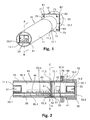
- Fig. 1
- eine perspektivische Darstellung eines röhrenförmigen Gehäuses mit einer darin angeordneten Blitzschutzschaltung auf einer Leiterplatine, wobei am vorderen stirnseitigen Ende eine Steckerbuchse für ein Netzwerkkabel angeorndet ist;
- Fig. 2
- ein Längsschnitt durch das Gehäuse aus
Fig. 1 entlang der Linie A - B; - Fig. 3
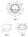
- ein Querschnitt durch das Gehäuse aus
Fig. 1 entlang der Linie C - D; - Fig. 4
- ein kreisförmige Scheibe mit einem nicht-radial verlaufenden Schlitz,;
- Fig. 5
- ein Verbindungsring mit einem innenseitigen Absatz;
- Fig. 6
- eine Leiterplatine mit einer Blitzschutzschaltung und zwei endseitig angeordneten Steckerbuchsen;
- Fig. 7
- eine Explosionsdarstellung des Gehäuses aus
Fig 1 mit kreisförmigen Scheibe und Verbindungsring; - Fig.8
- eine perspektivische Darstellung eines Gehäuses mit zwei planparallel übereinander angeordneten Leiterplatinen, welche je mit 6 Blitzschutzschaltungen bestückt sind;
- Fig. 9
- eine Frontansicht des Gehäuses aus
Fig. 8 .
- Fig. 1
- a perspective view of a tubular housing with a lightning protection circuit arranged therein on a printed circuit board, wherein at the front end end a socket for a network cable is angeorndet;
- Fig. 2
- a longitudinal section through the housing
Fig. 1 along the line A - B; - Fig. 3
- a cross section through the housing
Fig. 1 along the line C - D; - Fig. 4
- a circular disk with a non-radially extending slot;
- Fig. 5
- a connecting ring with an inside shoulder;
- Fig. 6
- a printed circuit board with a lightning protection circuit and two end-mounted sockets;
- Fig. 7
- an exploded view of the housing
Fig. 1 with circular disc and connecting ring; - Figure 8
- a perspective view of a housing with two plane-parallel superposed printed circuit boards, which are each equipped with 6 lightning protection circuits;
- Fig. 9
- a front view of the housing
Fig. 8 ,
Grundsätzlich sind in den Figuren gleiche Teile mit gleichen Bezugszeichen versehen.Basically, the same parts are provided with the same reference numerals in the figures.
In
Direkt hinter dem zweiten hohlzylindrischen Gehäuseteil 12 schliesst ein in
Am freien und ersten Ende 11.2 des ersten Gehäuseteils 11 (in
Die drei aus Aluminium bestehenden hohlzylindrischen Gehäuseteile 11, 12, 13 weisen, abgesehen von den beiden Befestigungsflanschen 70, 80, im Wesentlichen einen identischen Aussendurchmesser auf, welcher z. B. ca. 28 mm misst. Die gesamte Länge, gemessen in der Richtung der Längsachsen der drei koaxial angeordneten Gehäuseteile 11, 12, 13 beträgt beispielsweise ca. 112 mm.The three aluminum hollow
In
Im Bereich mit aufgeweitetem Innendurchmesser des zweiten Endes 11.2 des ersten Gehäuseteils 11 ist ein zylindrischer Verbindungsring 50 mit seiner halben Breite eingepresst. Die Längsachse des Verbindungsrings 50 ist dabei ebenfalls koaxial zu den Längsachsen des ersten und des zweiten Gehäuseteils 11, 12 ausgerichtet. Der Aussendurchmesser des Verbindungsrings 50 entspricht dabei in etwa dem aufgeweiteten Innendurchmesser des ersten Gehäuseteils 11 im Bereich des zweiten Endes 11.2 bzw. dem aufgeweiteten Innendurchmesser des zweiten Gehäuseteils 12 im Bereich des ersten Endes 12.1. Die andere Hälfte des Verbindungsrings 50 ist in gleicher Weise im Bereich mit aufgeweitetem Innendurchmesser des ersten Endes 12.1 des zweiten Gehäuseteils 12 eingepresst. Der minimale Innendurchmesser des Verbindungsrings 50 Bereich der engeren Ringöffnung 51 ungefähr gleich dem minimalen Innendurchmesser der ersten beiden Gehäuseteile 11, 12. Der Verbindungsring besteht z. B. aus Kupfer und verbindet die beiden ersten Gehäuseteile kraft- und formschlüssig miteinander.In the area with expanded inner diameter of the second end 11.2 of the
Im Bereich des zweiten Endes 12.2 des zweiten Gehäuseteils 12 weitet sich der Innendurchmesser des zweiten Gehäuseteils 12 ebenfalls stufenartig auf. Im Bereich des ersten Endes 13.1 des dritten Gehäuseteils 13 ist der Aussendurchmesser des dritten Gehäuseteils 13 stufenartig verjüngt und zwar so, dass er in etwa dem aufgeweiteten Innendurchmesser im Bereich des zweiten Endes 12.2 des zweiten Gehäuseteils 12 entspricht. Das erste und verjüngte Ende 13.1 des dritten Gehäuseteils liegt dabei im Bereich des zweiten Endes 12.2 des zweiten Gehäuseteils 12 vor und ist mit diesem kraft- und formschlüssig verpresst.In the region of the second end 12.2 of the
Die drei hohlzylindrischen Gehäuseteile sind daher mechanisch stabil miteinander verbunden und bilden zusammen das robuste röhrenförmige Gehäuse 10.The three hollow cylindrical housing parts are therefore mechanically stable connected to each other and together form the robust tubular housing 10th
Wie bereits bei
Am zweiten Ende 13.2 des dritten Gehäuseteils 13 ist zudem eine zylinderförmige Verschlusskappe 90 angeordnet, welche den dritten Gehäuseteil 13 verschliesst. Die Verschlusskappe 90 ist dabei als einseitig verschlossener Hohlzylinder ausgebildet, welcher den dritten Gehäuseteil 13 im Bereich seines zweiten bzw. Endes 13.2 aussen umgibt. Zur Befestigung der Verschlusskappe 90 ist z. B. ein an sich bekannter Bajonettmechanismus vorgesehen, so dass ein einfaches Lösen der Verschlusskappe 90 von Hand möglich ist.At the second end 13.2 of the
Der Inndendurchmesser des Verbindungsrings 50 weitet sich von seiner zweiten (in
In einem unteren Bereich der kreisförmigen Scheibe 60 ist des Weiteren ein nicht-radial verlaufender Schlitz 61 eingebracht (siehe hierzu auch
Am vorderen Ende 20.1 der Leiterplatine 20 ist zudem eine erste Steckerbuchse 31 direkt auf der Oberseite 20.5 der Leiterplatine 20 angeordnet, wobei es sich wie bei
Zwischen der ersten Steckerbuchse 31 und der kreisförmigen Scheibe 60 bzw. der Trennwand sind im ersten Teilraum 10.1 des Gehäuses 10 mehrere Elektronikbauteile 40 auf der Leiterplatine 20 angeordnet. Die Elektronikbauteile weisen eine geringe Höhe gegenüber der Leiterplatine 20 auf und sind sowohl an der Oberseite 20.5, wie auch an der Unterseite 20.4 der Leiterplatine 20 angeordnet.Between the
Im zweiten Teilraum 10.2 des Gehäuses 10, zwischen der kreisförmigen Scheibe 60 und der zweiten Steckerbuchse 32 sind an der Oberseite 20.5 der Leiterplatine 20 weitere Elektronikbauteile 41 angeordnet, welche von der Oberseite 20.5 der Leiterplatine 20 bis über die Längsmittelachse des Gehäuses 10 nach oben ragen.In the second subspace 10.2 of the
Ein in
Die beiden Teilräume 10.1 und 10.2 des Gehäuses 10 sind mit einer in
Die zweite Steckerbuchse 32 ist zudem von einer in
In
Die im zentralen Bereich von
Bis auf eine kleine Öffnung neben der rechten Seite der Leiterplatine 20 besteht wird der Schlitz 61 vollständig von der Leiterplatine 20 ausgefüllt oder durch das erste Gehäuseteil 11 abgedeckt. Zwischen dem ersten Gehäuseteil 11 und dem in
Ausserhalb des hohlzylindrischen ersten Gehäuseteils 11 ist in
In
In
Zusätzlich sind auf der Leiterplatine 20 zur Verbindung der Elektronikbausteine 40, 41 auf der Leiterplatine 20 übliche Leiterbahnen eingebracht, welche in
Zur Montage eines Gehäuses 10 mit Leiterplatine 20 wird in einem ersten Verfahrensschritt die fertig bestückte Leiterplatine 20 in den Schlitz 61 der kreisförmigen Scheibe 60 eingeschoben und anschliessend der Erdkontakt 20.6 auf der Leiterplatine 20 mit der kreisförmigen Scheibe verlötet. Im darauf folgenden Verfahrensschritt wird die kreisförmige Scheibe 60 mit eingebrachter Leiterplatine 20 von der Seite der weiten Ringöffnung 52 her durch den Verbindungsring 50 geschoben, bis die kreisförmige Scheibe 60 an der Stufe beim Übergang zur engen Ringöffnung 51 des Verbindungsrings 50 anschlägt. Anschliessend wird die eine Hälfte des Verbindungsrings 50 in den Bereich des zweiten Endes 11.2 des ersten Gehäuseteils 11 mit aufgeweitetem Innendurchmesser bis zum Anschlag eingepresst. Darauf folgend wird die andere Hälfte des Verbindungsring 50 in den Bereich des ersten Endes 12.1 des zweiten Gehäuseteils 12 mit aufgeweitetem Innendurchmesser ebenfalls bis zum Anschlag eingepresst. Scheibe 60 und Verbindungsring 50 werden miteinander verlötet.For mounting a
Im anschliessenden Verfahrensschritt wird das Gehäuse 10 mit seiner Längsachse in vertikaler Richtung gedreht und von oben her durch die stirnseitige Öffnung des ersten Endes 11.1 des ersten Gehäuseteils 11 Gussmasse eingefüllt. Nach einer kurzen Aushärtephase wird das Gehäuse um 180° gedreht, so dass die Gussmasse durch die Öffnung im Bereich des zweiten Endes 12.2 des zweiten Gehäuseteils 12 eingefüllt werden kann.In the subsequent method step, the
Im nächsten Verfahrensschritt erfolgt das Einpressen des ersten und verjüngten Endes 13.1 des dritten Gehäuseteils 13 im Bereich des zweiten Ende 12.2 des zweiten Gehäuseteils 12 mit aufgeweitetem Innendurchmesser.In the next method step, the pressing in of the first and tapered end 13.1 of the
In
Unterhalb der oberen Leiterplatine 120 ist eine planparallele angeordnete Leiterplatine untere 121 in gleicher Weise an den vier Haltestiften 161...164 befestigt.Below the upper printed
Im Bereich des hinteren Endes 120.2 der oberen Leiterplatine 120 sind insgesamt sechs Steckerbuchsen 131...136, welche vom Typ RJ 45 sind, direkt auf der Oberseite der oberen Leiterplatine 120 nebeneinander liegend angebracht. Entsprechend sind auf der unteren Leiterplatine 121 an deren hinterem Ende 121.2 ebenfalls insgesamt sechs weitere Steckerbuchsen 181...186, auch vom Typ RJ 45, direkt auf der Unterseite der untern Leiterplatine 121 nebeneinander liegend angebracht. Die Öffnungen sämtlicher Steckerbuchsen 131...136, 181, 186 ragen dabei in einer zur Frontplatte 111 entgegen gesetzten Richtung.In the region of the
In einem in
In den Eckbereichen der Frontplatte 111 sind insgesamt vier Befestigungsbohrungen 171...174 eingebracht, welche die Frontplatte vollständig durchdringen.In the corner regions of the front plate 111 a total of four mounting
In
Die beschriebenen Ausführungsformen sind lediglich als illustrative Beispiele zu verstehen, welche im Rahmen der Erfindung beliebig erweitert oder abgewandelt werden kann.The described embodiments are only to be understood as illustrative examples, which can be extended or modified as desired within the scope of the invention.
So ist es z. B. möglich, anstelle eines zylindrischen Gehäuses 10 in
Ebenso ist es denkbar, die Gehäuseteil 11, 12, 13 zusätzlich oder anstelle des Verpressens durch Verschraubung oder stoffschlüssige Verbindungen (Schweissen, Kleben, Löten) miteinander zu verbinden.It is also conceivable, the
Auch mehrere Trennwände, welche den Innenraum des Gehäuses 10 in mehr als zwei Teilräume unterteilen und die Leiterplatine 20 an mehreren Stellen zwischen dem vorderen Ende 20.1 und den hinteren Ende 20.2 abstützen sind möglich. Dabei kann die Robustheit und mechanische Festigkeit zusätzlich gesteigert werden.Also, several partitions, which divide the interior of the
Ebenso kann z. B. auch der dritte Gehäuseteil 13 mit einem weiteren Verbindungsring mit dem zweiten Gehäuseteil 12 verbunden werden.Likewise, z. B. also the
Auch in einem Gehäuse 10 gemäss
Grundsätzlich können natürlich auch Steckerbuchsen im Bereich der Mantelfläche des Gehäuses angebracht werden, wenn dies zweckdienlich ist und als Steckerbuchsen lassen sich auch andere Typen als die beschriebenen RJ 45 Steckerbuchsen verwenden. Weiter ist es denkbar, die Steckerbuchse 31 wegzulassen und stattdessen, das Kabel direkt auf die Leiterplatine zu löten.Basically, of course, sockets can be mounted in the region of the lateral surface of the housing, if this is expedient and as sockets other types can be used as the described RJ 45 sockets. Further, it is conceivable to omit the
Des Weiteren kann die kreisförmige Scheibe 60 z. B. auch ausserhalb des Verbindungsrings 50 direkt im ersten Gehäuseteil 11 oder im zweiten Gehäuseteil 12 angeordnet werden. Hierfür kann z. B. ein Absatz in einem der besagten Gehäuseteile angeordnet werden, welcher als Auflage für die Trennwand dient. Die Trennwand kann prinzipiell auch durch Verschraubung im Gehäuse 10 befestigt werden.Furthermore, the circular disc 60 z. B. outside the connecting
Anstelle einer Blitzschutzschaltung kann natürlich auch eine andere elektronische Schaltung auf der Leiterplatine 20 vorliegen.Of course, instead of a lightning protection circuit, another electronic circuit may also be present on the printed
Zusammenfassend ist festzustellen, dass ein äusserst kompaktes Gehäuse für Leiterplatinen geschaffen wurde, welches sich insbesondere durch eine hohe Robustheit und einfache Herstellung auszeichnet. Aufgrund der hohen mechanischen Belastbarkeit des Gehäuses ist eine Anwendung in Aussenbereichen, z. B. im militärischen Umfeld, problemlos möglich.In summary, it should be noted that an extremely compact housing for printed circuit boards has been created, which is characterized in particular by a high degree of robustness and ease of production. Due to the high mechanical strength of the housing is an application in outdoor areas, such. As in the military environment, easily possible.
Claims (18)
- Apparatus comprising a printed circuit board (20, 120, 121) for an electrical and/or electronic circuit, which printed circuit board is arranged in a housing (10, 100), the printed circuit board (20, 120, 121) having a front region (20.1, 120.1, 121.1) and a rear region (20.2, 120.2, 121.2), the printed circuit board (20, 120, 121) being mechanically supported in the housing (10, 100) between the front region (20.1, 120.1, 121.1) and the rear region (20.2, 120.2, 121.2), an internal space of the housing being separated into two subspaces (10.1, 10.2) by a partition wall (60),
characterized
in that the printed circuit board (20) projects through a slot (61) made in the partition wall (60) and is supported by the partition wall (60). - Apparatus according to Claim 1, characterized in that the slot (61) in the partition wall (60) is dimensioned in such a manner that it is completely filled by a region (20.3) of the printed circuit board (20) in the slot (61).
- Apparatus according to Claim 1 or 2, characterized in that the printed circuit board (20) is arranged perpendicular to the partition wall (60).
- Apparatus according to one of Claims 1-3, characterized in that the partition wall (60) consists of metal, in particular of copper, and is electrically connected to an electrical contact (20.6), in particular an earth contact, made in the printed circuit board (20).
- Apparatus according to Claim 4, characterized in that the electrical contact (20.6) made in the printed circuit board (20) is at least partially arranged in the slot (61) in the partition wall (60) and is soldered to the partition wall (60) for the purpose of making electrical contact.
- Apparatus according to one of Claims 1-5, characterized in that the partition wall (60) and the housing (10) are electrically connected.
- Apparatus according to one of Claims 1-6, characterized in that the housing (10) is tubular with a circular cross section, and in that the partition wall (60) is in the form of a circular disc which is oriented perpendicular to a longitudinal axis of the housing (10).
- Apparatus according to Claim 7, characterized in that the tubular housing (10) has a multi-part design, the end face of a first tubular housing part (11) being connected to a second tubular housing part (12) via an internally and coaxially arranged connecting ring (50).
- Apparatus according to Claim 8, characterized in that a first half of the connecting ring (50) is accommodated in a force-fitting and form-fitting manner in an end region (11.2) of increased internal diameter of the first tubular housing part (11), while a second half of the connecting ring (50) is simultaneously accommodated in a force-fitting and form-fitting manner in a second end region (12.1) of increased internal diameter of the second tubular housing part (12).
- Apparatus according to Claim 8 or 9, characterized in that the circular disc (60) is accommodated in the connecting ring (50), a diameter of the circular disc (60) corresponding to an internal diameter of the connecting ring (50), and the circular disc (60) preferably resting against an inwardly projecting protrusion of the connecting ring (50).
- Apparatus according to one of Claims 7-10, characterized in that the slot (61) in the circular disc (60) runs in a non-radial direction.
- Apparatus according to one of Claims 1-11, characterized in that the housing (10, 100) consists of metal, in particular of aluminium.
- Apparatus according to one of Claims 1-12, characterized in that a lightning protection circuit, in particular for a computer network connection, is arranged on the printed circuit board (20).
- Apparatus according to one of Claims 1-13, characterized in that the printed circuit board (20) is at least partially surrounded by a potting compound in order to protect against moisture and foreign bodies.
- Apparatus according to one of Claims 1-14, characterized in that a connector socket (31, 32) for electrical connection to an external cable is present on a front end face and/or on a rear end face of the housing (10), the connector socket (31, 32) preferably being directly fitted to the printed circuit board (20).
- Apparatus according to one of Claims 1-15, characterized in that the housing (10) has, on an outer side, one or more projections (70, 80) for fastening the housing (10) to a third element, the projections (70, 80) having fastening holes (71...74, 81...84), in particular.
- Apparatus according to one of Claims 1-16, characterized in that at least two printed circuit boards (120, 121) are arranged above one another in a plane-parallel manner and at a distance from one another.
- Method for producing a housing (10) having a printed circuit board (20) according to one of Claims 7-17, characterized in that a printed circuit board (20) is inserted into a slot (61) in a circular disc (60) and the disc (60) is then accommodated in a connecting ring (50) and a first half of the connecting ring (50) is then clamped in an end region (11.2) on the end face of a first tubular housing part (11) and a second half of the connecting ring (50) is then clamped in a second end region (12.1) of a second tubular housing part (12).
Applications Claiming Priority (1)
| Application Number | Priority Date | Filing Date | Title |
|---|---|---|---|
| CH3562008A CH706251B1 (en) | 2008-03-11 | 2008-03-11 | Enclosure with circuit board. |
Publications (3)
| Publication Number | Publication Date |
|---|---|
| EP2101554A2 EP2101554A2 (en) | 2009-09-16 |
| EP2101554A3 EP2101554A3 (en) | 2011-03-16 |
| EP2101554B1 true EP2101554B1 (en) | 2013-01-02 |
Family
ID=40756336
Family Applications (1)
| Application Number | Title | Priority Date | Filing Date |
|---|---|---|---|
| EP20090405030 Expired - Fee Related EP2101554B1 (en) | 2008-03-11 | 2009-02-16 | Casing with circuit board |
Country Status (2)
| Country | Link |
|---|---|
| EP (1) | EP2101554B1 (en) |
| CH (1) | CH706251B1 (en) |
Families Citing this family (1)
| Publication number | Priority date | Publication date | Assignee | Title |
|---|---|---|---|---|
| DE102009060872A1 (en) * | 2009-12-30 | 2011-08-18 | Baumer Innotec Ag | Sensor with housing and method for its manufacture |
Family Cites Families (5)
| Publication number | Priority date | Publication date | Assignee | Title |
|---|---|---|---|---|
| US4400858A (en) * | 1981-01-30 | 1983-08-30 | Tele-Drill Inc, | Heat sink/retainer clip for a downhole electronics package of a measurements-while-drilling telemetry system |
| US5034856A (en) * | 1989-10-24 | 1991-07-23 | Hewlett-Packard Company | Modular housing assembly for two incompatible circuits |
| EP0986293A1 (en) * | 1998-09-08 | 2000-03-15 | Lucent Technologies Inc. | Radio frequency electronic apparatus |
| DE20115670U1 (en) * | 2001-09-24 | 2002-02-21 | Trw Automotive Electron & Comp | Housing for an electronic control unit in vehicles |
| US7048564B1 (en) * | 2005-05-27 | 2006-05-23 | Delphi Technologies, Inc. | Sealed electronic module with fastenerless circuit board support post |
-
2008
- 2008-03-11 CH CH3562008A patent/CH706251B1/en not_active IP Right Cessation
-
2009
- 2009-02-16 EP EP20090405030 patent/EP2101554B1/en not_active Expired - Fee Related
Also Published As
| Publication number | Publication date |
|---|---|
| EP2101554A2 (en) | 2009-09-16 |
| EP2101554A3 (en) | 2011-03-16 |
| CH706251B1 (en) | 2013-09-30 |
Similar Documents
| Publication | Publication Date | Title |
|---|---|---|
| DE3790062C2 (en) | ||
| EP0921609A2 (en) | Right angled HF coaxial connector | |
| EP3164911B1 (en) | Plug | |
| DE10392323B4 (en) | Printed circuit board containing electrical connector assembly | |
| DE2845234A1 (en) | CONTACT DEVICE FOR MULTI-LAYER CIRCUITS | |
| DE202006000720U1 (en) | HF plug-fastening means | |
| DE202005017012U1 (en) | Electrical connection device for a printed circuit board | |
| EP3435482A1 (en) | Connection piece with a cable assembly and a plate assembly, and a plate assembly for a connection piece, and a method for producing such a connection piece | |
| EP4014287A1 (en) | 8 + 2 way xlr pcb female connector | |
| DE3710394C2 (en) | ||
| DE60008719T2 (en) | INPUT / OUTPUT CONNECTOR ASSEMBLY WITH GROUNDING ARRANGEMENT FOR SHIELDED CABLES AND METHOD FOR PRODUCING AND ASSEMBLING SUCH A CONNECTOR | |
| DE3313967A1 (en) | Device for the reliable production of electrically conductive connections between housing parts of a housing | |
| EP2101554B1 (en) | Casing with circuit board | |
| DE7429478U (en) | Connectors for electronic devices | |
| DE202012002352U1 (en) | Arrangement of plug connector and circuit board | |
| DE19720678C1 (en) | RF coaxial connector part | |
| EP0606294A1 (en) | Structure of an electrotechnical device | |
| EP0918374B1 (en) | High Frequency coaxial connector | |
| AT505742B1 (en) | ELECTRONIC DEVICE | |
| DE102007039064A1 (en) | Electronic device for use as control device for pump, has plug connector with two connector pins and contact holder holding connector pins and connector pin is arranged above and below printed circuit board | |
| DE102012005812A1 (en) | Electrical connector with integrated impedance matching element | |
| DE10017239A1 (en) | Tuner unit has pressure device on frame bearer that presses surface of protrusion, which is inserted into main card opening, with connection conductor image towards second conductor image | |
| DE102010027990A1 (en) | USB socket | |
| DE3802642C1 (en) | Electrical plug distributor | |
| DE102014012739A1 (en) | Electrical connector, connector element and use |
Legal Events
| Date | Code | Title | Description |
|---|---|---|---|
| PUAI | Public reference made under article 153(3) epc to a published international application that has entered the european phase |
Free format text: ORIGINAL CODE: 0009012 |
|
| AK | Designated contracting states |
Kind code of ref document: A2 Designated state(s): AT BE BG CH CY CZ DE DK EE ES FI FR GB GR HR HU IE IS IT LI LT LU LV MC MK MT NL NO PL PT RO SE SI SK TR |
|
| AX | Request for extension of the european patent |
Extension state: AL BA RS |
|
| PUAL | Search report despatched |
Free format text: ORIGINAL CODE: 0009013 |
|
| AK | Designated contracting states |
Kind code of ref document: A3 Designated state(s): AT BE BG CH CY CZ DE DK EE ES FI FR GB GR HR HU IE IS IT LI LT LU LV MC MK MT NL NO PL PT RO SE SI SK TR |
|
| AX | Request for extension of the european patent |
Extension state: AL BA RS |
|
| 17P | Request for examination filed |
Effective date: 20110830 |
|
| AKX | Designation fees paid |
Designated state(s): CH DE LI |
|
| GRAP | Despatch of communication of intention to grant a patent |
Free format text: ORIGINAL CODE: EPIDOSNIGR1 |
|
| GRAS | Grant fee paid |
Free format text: ORIGINAL CODE: EPIDOSNIGR3 |
|
| GRAA | (expected) grant |
Free format text: ORIGINAL CODE: 0009210 |
|
| AK | Designated contracting states |
Kind code of ref document: B1 Designated state(s): DE |
|
| RBV | Designated contracting states (corrected) |
Designated state(s): DE |
|
| REG | Reference to a national code |
Ref country code: DE Ref legal event code: R096 Ref document number: 502009005872 Country of ref document: DE Effective date: 20130307 |
|
| PLBE | No opposition filed within time limit |
Free format text: ORIGINAL CODE: 0009261 |
|
| STAA | Information on the status of an ep patent application or granted ep patent |
Free format text: STATUS: NO OPPOSITION FILED WITHIN TIME LIMIT |
|
| 26N | No opposition filed |
Effective date: 20131003 |
|
| REG | Reference to a national code |
Ref country code: DE Ref legal event code: R097 Ref document number: 502009005872 Country of ref document: DE Effective date: 20131003 |
|
| PGFP | Annual fee paid to national office [announced via postgrant information from national office to epo] |
Ref country code: DE Payment date: 20190219 Year of fee payment: 11 |
|
| REG | Reference to a national code |
Ref country code: DE Ref legal event code: R119 Ref document number: 502009005872 Country of ref document: DE |
|
| PG25 | Lapsed in a contracting state [announced via postgrant information from national office to epo] |
Ref country code: DE Free format text: LAPSE BECAUSE OF NON-PAYMENT OF DUE FEES Effective date: 20200901 |