EP2101455A2 - Apparatus and Method for Decision Feedback Equalization - Google Patents
Apparatus and Method for Decision Feedback Equalization Download PDFInfo
- Publication number
- EP2101455A2 EP2101455A2 EP09155188A EP09155188A EP2101455A2 EP 2101455 A2 EP2101455 A2 EP 2101455A2 EP 09155188 A EP09155188 A EP 09155188A EP 09155188 A EP09155188 A EP 09155188A EP 2101455 A2 EP2101455 A2 EP 2101455A2
- Authority
- EP
- European Patent Office
- Prior art keywords
- data
- edge
- dfe
- odd
- rate
- Prior art date
- Legal status (The legal status is an assumption and is not a legal conclusion. Google has not performed a legal analysis and makes no representation as to the accuracy of the status listed.)
- Withdrawn
Links
Images







Classifications
-
- H—ELECTRICITY
- H04—ELECTRIC COMMUNICATION TECHNIQUE
- H04L—TRANSMISSION OF DIGITAL INFORMATION, e.g. TELEGRAPHIC COMMUNICATION
- H04L25/00—Baseband systems
- H04L25/02—Details ; arrangements for supplying electrical power along data transmission lines
- H04L25/03—Shaping networks in transmitter or receiver, e.g. adaptive shaping networks
- H04L25/03878—Line equalisers; line build-out devices
- H04L25/03885—Line equalisers; line build-out devices adaptive
-
- H—ELECTRICITY
- H04—ELECTRIC COMMUNICATION TECHNIQUE
- H04L—TRANSMISSION OF DIGITAL INFORMATION, e.g. TELEGRAPHIC COMMUNICATION
- H04L25/00—Baseband systems
- H04L25/02—Details ; arrangements for supplying electrical power along data transmission lines
- H04L25/03—Shaping networks in transmitter or receiver, e.g. adaptive shaping networks
- H04L25/03006—Arrangements for removing intersymbol interference
- H04L25/03012—Arrangements for removing intersymbol interference operating in the time domain
- H04L25/03019—Arrangements for removing intersymbol interference operating in the time domain adaptive, i.e. capable of adjustment during data reception
- H04L25/03057—Arrangements for removing intersymbol interference operating in the time domain adaptive, i.e. capable of adjustment during data reception with a recursive structure
-
- H—ELECTRICITY
- H04—ELECTRIC COMMUNICATION TECHNIQUE
- H04L—TRANSMISSION OF DIGITAL INFORMATION, e.g. TELEGRAPHIC COMMUNICATION
- H04L25/00—Baseband systems
- H04L25/38—Synchronous or start-stop systems, e.g. for Baudot code
- H04L25/40—Transmitting circuits; Receiving circuits
- H04L25/49—Transmitting circuits; Receiving circuits using code conversion at the transmitter; using predistortion; using insertion of idle bits for obtaining a desired frequency spectrum; using three or more amplitude levels ; Baseband coding techniques specific to data transmission systems
- H04L25/4906—Transmitting circuits; Receiving circuits using code conversion at the transmitter; using predistortion; using insertion of idle bits for obtaining a desired frequency spectrum; using three or more amplitude levels ; Baseband coding techniques specific to data transmission systems using binary codes
-
- H—ELECTRICITY
- H04—ELECTRIC COMMUNICATION TECHNIQUE
- H04L—TRANSMISSION OF DIGITAL INFORMATION, e.g. TELEGRAPHIC COMMUNICATION
- H04L25/00—Baseband systems
- H04L25/02—Details ; arrangements for supplying electrical power along data transmission lines
- H04L25/03—Shaping networks in transmitter or receiver, e.g. adaptive shaping networks
- H04L25/03006—Arrangements for removing intersymbol interference
- H04L2025/0335—Arrangements for removing intersymbol interference characterised by the type of transmission
- H04L2025/03356—Baseband transmission
Definitions
- This application is based upon and claims the benefit of the priority of Japanese patent application No. 2008-066222 filed on March 14, 2008 , the disclosure of which is incorporated herein in its entirety by reference thereto.
- This invention relates to a method and apparatus for decision feedback equalization and, more particularly, to edge timing detection following the decision feedback equalization.
- ISI inter-symbol interference
- DFE decision feedback equalization
- the DFE is a waveform equalization technique that negatively feeds back an amount of succeeding ISI(Inter-Symbol Interference), corresponding to the result of decision of a received signal by a data decision circuit, to succeeding bits to remove ISI.
- ISI Inter-Symbol Interference
- the DFE in which the period of the feedback signal is the data rate period (T) is termed the 'full-rate DFE', and the DFE in which the period of the feedback signal is twice the data rate period (2T) is referred to as 'half-rate DFE'.
- the data rate communication of 10 Gb/s is implemented using a differential clock of 5GHz.
- DFE-equalized added signals 122 and 122 are interleave-sampled by an odd data sampling unit 113 and an even data sampling unit 123, respectively, at a timing of an odd half-rate clock 118 and at a timing of an even half-rate clock 128, respectively.
- Odd sampling data 114 from the odd data sampling unit 113 and even sampling data 124 from the even data sampling unit 123 are multiplied by tap gains 117 and 127, respectively.
- An output of the tap gain 127 which is the odd DFE decision feedback signal 116, is negatively fed back to the odd DFE adder 111 as a signal to be added.
- An output of the tap gain 117 which is the even DFE decision feedback signal 126, is negatively fed back to the even DFE adder 121 as a signal to be added.
- This DFE equalization by negative feedback removes ISI to enable correct data reception.
- a decision feedback signal corresponding to an odd sampling data d1 multiplied by a tap gain ( ⁇ ), to generate a DFE-equalized even added signal: d ⁇ 2 + ⁇ ⁇ d ⁇ 1
- This DFE-equalized waveform is correctly sampled at an even half-rate clock to yield an even sampling data d2 with a period of 2T.
- This DFE equalized waveform is correctly sampled at an even half-rate clock to generate even sampling data d2 with the period of 2T.
- the odd DFE decision feedback signal 116 is added in this odd DFE adder 111 to the received signal d3 so that the signal d3 is DFE-equalized.
- the double-data rate system samples data at a half-rate clock
- the sampling data is of the period 2T equal to twice the data rate period T.
- one of two signals to be added in the DFE adder is a received signal of the sampling data period of 2T, while the other is a received signal of the data rate period T.
- the data waveform-equalized by DFE of Fig.1 is only data at an odd or even sampling timing.
- the signals output from the DFE adders may be waveform equalized only at a rate of one per two data at each of the even and odd sides.
- a waveform which is an alternate repetition of waveform-equalized open eye data and non-waveform-equalized closed eye data, as shown in Fig.4 .
- Non-Patent Document 1 The entire disclosure of Non-Patent Document 1 is incorporated herein by reference thereto. The following analyses are given by the present invention.
- a clock signal is ordinarily not transmitted.
- a clock recovery circuit abbreviated to 'CDR', which is configured to reproduce a clock signal from received data, is provided in a receiving side.
- Fig.3 shows examples of full-rate DFE equalized eye pattern and edge distributions. From these edge distributions, the low-pass filtering function proper to the CDR extracts a distribution center to adjust a rising edge of a data sampling clock to a center position between the neighboring edges extracted to enable correct data sampling.
- a decision feedback equalization apparatus comprising an odd data receiving unit that receives an odd data sampling clock, an odd edge sampling clock and a DFE input signal and that includes a half-rate DFE equalization function, and an even data receiving unit that receives an even data sampling clock, an even edge sampling clock and the DFE input signal and that includes a half-rate DFE equalization function.
- the odd data receiving unit includes a data detection means and an edge detection means on a half-rate DFE equalized signal.
- the even data receiving unit include a data detection means and an edge detection means on a half-rate DFE equalized signal.
- the apparatus also comprises a pattern filter that receives a set of sampling data by the detection means and that detects a data pattern, three consecutive bits of which are 110 or 001.
- the pattern filter selects edge data based on a result of the detection so that edge data on the half-rate DFE equalized signal will be selected only on detection of the data pattern of 110 or 001.
- clock recovery is executed on the basis of the output of the decision feedback equalizer.
- a decision feedback equalization apparatus comprising an odd data receiving unit that receives an odd data sampling clock, an odd edge sampling clock and a DFE input signal and that includes a half-rate DFE equalization function, and an even data receiving unit that receives an even data sampling clock, an even edge sampling clock and the DFE input signal and that includes a half-rate DFE equalization function.
- the odd data receiving unit includes a data detection means, an edge detection means for detection on a half-rate DFE equalized signal, and an edge detection means for detection on a non-half-rate DFE equalized signal.
- the even data receiving unit includes a data detection means and an edge detection means for detection on a half-rate DFE equalized signal and an edge detection means for detection on a non-half-rate DFE equalized signal.
- the apparatus also comprises a pattern filter that includes means for receiving a set of sampling data by the detection means and for detecting a data pattern three consecutive bits of which are 110 or 001 and a data pattern three consecutive bits of which are 101 or 010.
- the means of the pattern filter selects edge data based on a result of the detection so that edge data on the half-rate DFE equalized signal will be selected on detection of the data pattern of 110 or 001 and so that edge data on the non-half-rate DFE equalized signal will be selected on detection of the data detection pattern of 101 or 010.
- the present invention it is possible to adjust the phase of the recovered clock in case of using half-rate decision feedback equalization. According to the present invention, it is possible to suppress distributions of the recovered clock and to improve data sampling accuracy as well as the communication quality.
- an odd data receiving unit an even data receiving unit, and a pattern filter.
- the odd data receiving which receives an odd data sampling clock, an odd edge sampling clock and a DFE input signal, includes a half-rate DFE equalization function.
- the even data receiving unit which receives an even data sampling clock, an even edge sampling clock and a DFE input signal, includes a half-rate DFE equalization function.
- the even data receiving unit and the odd data receiving unit each includes a data detection unit and an edge detection unit for data and edge detection on a half-rate DFE equalized signal.
- the pattern filter receives a set of sampling data by the detection units and includes a detection unit that detects a data pattern of three consecutive bits of 110 or 001 and that operates based on the detected result to select edge data on the half-rate DFE equalized signal only in case the detected pattern is the 110 or 001 pattern.
- an odd data receiving unit an even data receiving unit, and a pattern filter.
- the odd data receiving unit which receives an odd data sampling clock, an odd edge sampling clock and a DFE input signal, includes a half-rate DFE equalization function.
- the even data receiving unit which receives an even data sampling clock, an even edge sampling clock and a DFE input signal, includes a half-rate DFE equalization function.
- the even data receiving unit and the odd data receiving unit each includes a data detection unit and an edge detection unit for data and edge detection on a half-rate DFE equalized signal, and an edge detection unit for edge detection on a non-half-rate DFE equalized signal.
- the pattern filter receives a set of sampling data by the detection units and includes a detection unit that detects a data pattern of three consecutive bits of 110 or 001 and a data pattern of three consecutive bits of 101 or 010.
- the pattern filter operates based on the detected result to select edge data on the half-rate DFE equalized signal in case the data pattern is the 110 or 001 pattern as well as to select edge data on the non-half-rate DFE equalized signal in case the data pattern is the 101 or 010 pattern.
- the pattern selector may be simplified in configuration by combining the pattern filter with the edge detection unit provided in the CDR.
- the pattern filter includes an EXOR operating mechanism for a detected data string of consecutive bits of the half-rate DFE equalized signal and a mechanism that selects the result of edge detection on the half-rate DFE equalized signal or the result of edge detection on the non-half-rate DFE equalized signal based on the result of the operation.
- an amplitude error sampling mechanism capable of adjusting a sampling threshold value to enable adaptive DFE equalization, thereby enabling adaptive DFE equalization in the receiving circuit.
- a decision feedback signal optimized to the ISI, influencing given data, has a period twice the data rate (2T).
- the wide-range edge distribution of (B) of Fig.4 may be attributed to the fact that the decision feedback signal with a 2-bit width is optimized for the first bit data, while it is not optimized for the second bit data.
- the decision feedback signal optimized for the first bit, is added to the waveform of the second bit, even though the value of the first bit differs from the second bit. Hence, the decision feedback signal, which is not proper, is added to the waveform of the second bit, thus closing one of the eye patterns.
- the two data are influenced similarly by the ISI, so that the two data are waveform-equalized in a proper manner.
- the full-rate DFE, shown in Fig.3 and the half-rate DFE, are of the same edge distribution.
- the half-rate clock phase may correctly be adjusted by the CDR.
- Fig.5 depicts a timing diagram for illustrating an example of the operation of the half-rate DFE for removing the influencing quantity of ISI for the trailing 5 bits, referred to below as 5-tap DFE. It is noted however that the present invention is not limited to the number of taps equal to 5.
- the received data are separated into two parallel paths.
- the data at the sampling timing of these two paths are waveform-equalized by half-rate DFE.
- the two parallel paths are termed 'an odd data sampling path' and 'an even data sampling path' in the description to follow.
- the odd data sampling path samples a data string of d1, d3, d5 and so forth, while the even data sampling path' samples a data string of d2, d4, d6 and so forth.
- the odd and even data sampling paths sample the data alternately.
- the signal In order for the non-sampling data signal of the equation (11) to be correctly equalized by DFE, the signal must be equal in signal level to the following signal for full-rate DFE:
- the waveform obtained with the half-rate DFE is equivalent to that obtained with the full-rate DFE. That is, under those conditions, the edges of the same timing may be extracted with the half-rate DFE as with the full-rate DFE.
- condition (b) is excluded because it means that DFE tap coefficients are all zero and hence that equalization is not used.
- condition (a) represents the condition under which the correct edge that is desirably used may be obtained.
- the condition under which the same edge timing may be obtained with the half-rate DFE as with full-rate DFE is that the same data occurs in succession before occurrence of data transition.
- data before d6 are preferably the same data for all time. However, such indicates that the same data are transmitted for all time.
- the data transmission of this sort may, of course, not be entitled to data communication.
- wn where n is 0, 1, 2 and so forth, are coefficients for correcting for an amount of ISI. These coefficients are determined by the amount of ISI on trailing side bits.
- the first backward ISI amount w1 is appreciably larger than the second and the following ISI amount w2, w3 and so forth.
- the tendency of wl>> w2, w3, w4 and so forth is outstanding.
- edge is to be detected from the waveform after passage through the half-rate DFE stage, only such data transitions in which data directly before the edge and data two bits before the edge are the same, more specifically, in which the data sequence is of a pattern of "0 ⁇ 0 ⁇ 1" or "1 ⁇ 1 ⁇ 0", need to be detected by a pattern filter and used as edge data for the CDR. That is, doing so detects an edge timing similar to that in case of the full-rate DFE. It should be noted that, in the above discussions, the transmission of binary signals of "0" and "1" is presupposed.
- the processing of filtering by the pattern filter enables detection of the edge similar to that detected with the full-rate DFE.
- another problem connected with a deteriorated jitter tolerance characteristic of a CDR may be incurred.
- the present invention proposes detecting the edges of data transitions from 010 and 101 from a waveform not equalized by half-rate DFE.
- the eye patterns of the waveforms, received before DFE, are closed.
- the frequency components of patterns of "01" alternations are substantially constant, and hence the ISI is small.
- the edge variations are small, such that filtering may sufficiently be achieved with a low-pass filter (LPF) ordinarily used as the CDR function.
- LPF low-pass filter
- edges of 010 and 101 data and those of 110 and 110 data are received simultaneously by parallel paths. However, there is produced a difference in delay depending on whether or not the data have been passed through the DFE circuit.
- the edge path for 010 data and for 101 data may cancel the signal delay difference by transmitting the data through a adder of zero DFE coefficient or by having delay included into the signal.
- the result is suppression of distribution of the recovered clock and improved accuracy in data sampling and in communication quality (bit error rate).
- Fig.7 is a schematic view showing a configuration of an edge detection block, employing half-rate DFE, according to an exemplary embodiment of the present invention.
- an input signal 700 is interleave-sampled in an odd data receiving unit 710 and an even data receiving unit 720, each at a half clock rate.
- two pairs of differential half-rate clocks, each with a phase offset of 90 degrees are used for sampling the input signal.
- the input signal is subjected to double over-sampling at even data timing, odd data timing and at edge timings.
- the odd data timing clock is clk0
- the odd edge timing clock is clk90, with a phase shift of 90 degrees from clk0
- the even data timing clock is clk180
- the even edge timing clock is clk270, with a phase shift of 270 degrees from clk0.
- the odd data receiving unit 710 and the even data receiving unit 720 are each provided with a mechanism for sampling the half-rate DFE equalized waveform at a data timing and at an edge timing, and a mechanism for sampling the non-half-rate DFE equalized waveform at an edge timing.
- the even data receiving unit 720 receives the even data from the even data receiving unit 720.
- a pattern filter 730 which receiving the above sampling data, selects, out of two sorts of the edge decision data (712 and 713; 722 and 723), sampled at odd and even edge timings, one of two sets of the edge timing data, depending on a data pattern of three consecutive bits, obtained from the data decision data 711 and 721 sampled at the odd and even data timings.
- Edge decision data 714 and 724 and data decision data 715 and 725, thus selected, are supplied to a phase comparator 740 of the CDR for use for a data reproducing operation by the CDR.
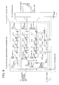
- Fig.9 shows an example of an arrangement of the odd data receiving unit 710 of Fig.7 .
- the even data receiving unit 720 of Fig.7 is symmetrical with respect to the arrangement of the odd data receiving unit 710. If the odd-even relationship is interchanged, the clock clk0 (180) is interchanged with the clock clk180 (0) and the clock clk90(270) is interchanged with the clock clk270 (90), the result is that the data receiving units 710, 720 are interchanged with each other.
- the input signal 700 is branched to the odd data receiving unit 710 and to the even data receiving unit 720 so as to be then delivered to a DFE equalized waveform processing unit 900 and to a non-DFE equalized waveform processing unit 901 provided in each of the two data receiving units 710 and 720.
- a DFE adder 911 adds an input signal 100 and a decision feedback signal 916 together to output a DFE equalized signal 917.
- the DFE equalized signal 917 is sampled with clk0 by a data sampling unit 912, while being sampled with clk90 by an edge sampling unit 922.
- the data decision data, sampled by the data sampling unit 912, are negatively fed back via a set of latches 913 and a set of tap gains 915 as a feedback decision signal 916 for use for DFE processing by the DFE adder 911.
- Outputs of the odd stages of the tap gains 915-1, 915-3 and so forth in the odd data receiving unit 710 are delivered to associated odd adders 914-1, 914-3 and so forth of the even data receiving unit 720 (726 in Fig.7 ), respectively.
- Those outputs of the odd stage tap gains are then added to outputs of even stage tap gains 915-2, 915-4 and so forth of the even data receiving unit 720 to generate a decision feedback signal 918 which is then fed back to the DFE adder 911.
- Outputs of odd stage tap gains 915-1, 915-3 and so forth in the even data receiving unit 720 are delivered to associated odd adders 914-1, 914-3 and so forth of the odd data receiving unit 710 (727 in Fig.7 ), respectively so as to be then added to outputs of the even stage tap gains 915-2, 915-4 and so forth of the odd data receiving unit 710 to generate a decision feedback signal 918 which is then fed back to the DFE adder 911.
- the tap gain 915 is a gain stage corresponding to wn of the equation (I), where n denotes a natural number.
- the data decision data are output as odd data decision data 711 to the pattern filter 730.
- the data decision data 711 is output from the last latch of the set of the latches 913, it does not matter from which latch the data is branched and output to the pattern filter.
- the edge decision data, sampled by the edge sampling unit 922, is then delay-adjusted by a set of latches 923 so as to be output as the odd half-rate DFE equalized edge decision data 712 to the pattern filter 730.
- the input signal 700 is delayed by delay adjustment 931 in an amount equivalent to the delay of the DFE adder 911.
- An edge sampling unit 932 samples the edge decision data of the non-DFE equalized waveform with the clock clk90 of the same timing as the sampling timing of the edge sampling unit 922.
- Fig.9 there is shown an instance of delay adjustment 931 in which delay is adjusted using a dummy adder of the same configuration as the DFE adder 911 with one of input signals being a zero.
- An output of the edge sampling unit 932 is delay-adjusted by a set of latches 933, in the same way as the edge decision data is delay-adjusted by the set of latches 923.
- the so delay-adjusted output of the edge sampling unit is output to the pattern filter 730. It should be noted however that delay adjustment is made at the data receiving units 710 and 720 to permit the pattern filter 730 to discriminate time-domain data obtained on sampling the data decision data 711 and that obtained on sampling the edge decision data 712 and 713.
- Fig.9 shows an example in which decision feedback signals of all tap outputs of DFE are added by the DFE adders 914 to form the decision feedback signal 916 before delivery to the DFE adder 911.
- the present invention is not limited to this configuration. It does not matter which configuration is used provided that decision feedback signals of all taps are added at the output of the DFE adder 911 such as by directly summing the decision feedback signal of each tap at each DFE adder.
- the waveform-processed data, thus generated, are output to the pattern filter 730 to select edge decision data.
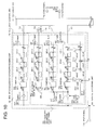
- Fig.10 shows a configuration of a front end of half-rate DFE provided with an offset canceling mechanism in case the sampling path and the sampling unit, needed for adjusting the DFE equalization coefficients, are arranged in a differential configuration.
- a sampling path for sampling the half-rate DFE equalized waveform by an amplitude error sampling unit 942 is provided in parallel with the data sampling unit 912 of Fig.9 .
- the amplitude error sampling unit 942 samples the result of comparison of an error decision reference potential 948 (Vref) on the half-rate DFE equalized signal 917 at a timing corresponding to clk0, as in the data sampling unit 912.
- Vref error decision reference potential
- the amplitude error sampling unit 942 adjusts the delay in its output using e.g. a set of latches 943, as in the data sampling unit 912.
- the output of the amplitude error sampling unit is delivered to a demultiplexer (DEMUX) 750, as is the data decision data 711.
- DEMUX demultiplexer
- the sampling units may be of a single-ended configuration or of a differential configuration.
- the differential configuration there is a possibility that the sampling units 912, 922, 932 and 942 give a mistaken data decision due to an offset voltage of the differential pair generated in the sampling units 912, 922, 932 and 942 passed through by the signal.
- sampling units may each be provided with an offset correction mechanism to improve the bit error rate (BER).
- BER bit error rate
- Fig.11 shows an example of a differential flip-flop of the sampling unit.
- Fig.12 shows an example of an offset canceling mechanism for the differential flip-flop.
- a differential input 1201 (in, inb) is delivered to a differential transistor pair (1221, 1222) of a master latch 1202.
- Clocks clk1205 and clk1206 form a differential clock pair.
- a transistor 1229 is turned on by clkb1205
- an input is accepted, that is, the differential transistor pair (1221, 1222) is activated.
- a transistor 1230 is turned on by clk1206, the signal so accepted is latched. Simultaneously, the latched signal is delivered to a differential transistor pair (1225, 1226) of a slave latch 1203.
- the signal accepted by the slave latch is latched.
- the so latched signal is delivered as a differential output 1204 to the latches 912, 922, 932 and 942 of the next stage and to the tap gains 915.
- a differential latch with a single output may also be used.
- Fig.12 shows an example of the latter mechanism.
- a differential input is delivered to two differential pairs (1320, 1321) and (1322, 1323), the drain terminals of which are connected in common.
- the transistors 1320 and 1323 are equal in size to each other, while the transistors 1321 and 1322 are also equal in size to each other.
- the ratio of driving capabilities of the transistors 1320 and 1321 is set to M:1, while that of the transistors 1323 and 1322 is also set to M:1.
- the source terminals of the differential transistor pair (1320, 1321) are connected in common to a variable current source 1310, while the source terminals of the differential transistor pair (1322, 1323) are connected to a variable current source 1312.
- the current amounts of the variable current sources 1310 and 1312 are controlled by current amount control signals 1311 and 1313, respectively.
- the ratio of current amounts of the variable current sources 1310 and 1312 is controlled by an externally controlled digital-to-analog converter DAC, by way of controlling the current amount, thereby generating different offsets at a differential output 1304.
- reception sensitivity may be improved over the case of not providing the offset canceling mechanism.
- it is unnecessary to increase the gate area for lowering the offset voltage.
- decision feedback signals of all of the DFE tap outputs are added by the adder 914, before being supplied to the DFE adder 911, to constiture the decision feedback signal 916.
- the present invention is not limited to this configuration. It does not matter which configuration is used provided that decision feedback signals of all taps are added at the output of the DFE adder 911 such as by directly summing the decision feedback signals of the respective taps at the respective DFE adders.
- Fig.13 shows an example of directly adding the decision feedback signals of the respective taps by the DFE adder 911.
- a signal at a differential input 1401 is supplied to a differential amplifier circuit of the initial stage made up of a current source 1410, a differential pair (1420, 1421) and load resistors 1424.
- a first decision feedback signal 1441, a second decision feedback signal 1442 and so forth up to an n'th decision feedback signal 1443 are negatively fed back to a differential output 1404.
- Fig.13 shows an example in which the decision feedback signal is differential.
- the first decision feedback signal 1441 is differentially delivered to the gates of a differential transistor pair (1422, 1423), the sources of which are connected in common and connected to a first variable current source 1411 and the drains of which are connected to the differential output 1404.
- the n'th decision feedback signal 1443 is differentially delivered to the gates of a differential transistor pair (1426, 1427), the sources of which are connected in common and connected to the n'th variable current source 1413 and the drains of which are connected to the differential output 1404.
- Sign adjustment of the respective decision feedback signals is by any of suitable routine techniques (known techniques), although such technique is not shown in Fig.13 .
- the tap gain for each decision signals may be generated by controlling the first, second and n'th variable current sources 1411, 1412 and 1413 by current control signals 1431, 1432 and 1433, respectively.
- the operation equivalent to that of the tap gain 915 may thereby be carried out simultaneously.
- common mode control by common mode negative feedback 1402 is carried out for the differential output 1404.
- the waveform-processed data, thus generated, is delivered to the pattern filter 730 where edge decision data is selected.
- data decision data and edge decision data may be obtained from the half-rate DFE equalized waveform, while edge decision data may be obtained from the non-half rate DFE decision data, in accordance with an interleaving system.
- the configuration of the pattern filter 730 which generates the edge timing of the same timing as that obtained with full-rate DFE from the half-rate DFE equalized data and from non-half rate DFE decision data, will now be described.
- the data transition timing of the half rate DFE equalized data and that of the non-half rate DFE decision data become approximately equal to the data transition timing of the full-rate DFE equalized data.
- the data transition timing of the non-half rate DFE equalized data becomes approximately equal to the data transition timing of the full-rate DFE equalized data.
- a commonplace logic may be used.
- a 3-bit pattern filter has a wide area.
- the pattern filter 730 effects pattern filtering of former two of the three bits and an edge detection means of the phase comparator 740 is used in combination to effect pattern filtering of three bits of 110 and 001 as well as 101 and 010 to reduce the pattern filter size.
- a generally used double rate over-sampling CDR includes the customary phase comparator 740 for comparing a signal phase with a clock phase to detect data transition (edge) needed for clock recovery, and thus has the function of detecting an edge timing.
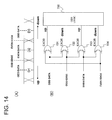
- Fig.14 shows an example of the phase comparator 740.
- the phase comparator 740 performs
- Fig.15 shows examples of phase detection by the phase detector of Fig.13 .
- a CDR logic 750 then exercises control to shift the clock phase towards the up-side.
- a mechanism for detecting the presence or non-presence of data transition (edge) for phase adjustment of the reproduced clock is equipped in the CDR.
- This edge detection means may be used in place of pattern filtering of latter two bits of the three-bit pattern filter.
- phase comparator 740 it is unnecessary to filter a data string in the pattern filter 730 insofar as the transitions of the second and third bits 01 and 10 of the 001 and 110 patterns as the target data pattern, as well as those of the second and third bits 01 and 10 of the 101 and 010 patterns as the other target data pattern. It is only necessary to discriminate whether or not the former two bits are 00 and 11 as well as 01 and 10. As a result, the pattern filter may be simplified.
- the result of the exclusive-OR (EXOR) operation on the former two bits (00, 11) is 0, insofar as detection of 001 and 110 patterns is concerned, while the result of the EXOR operation on the former two bits (01, 10) is 1, insofar as detection of 101 and 010 patterns is concerned
- Fig.16 summarizes the operation of the present Example.
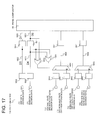
- Fig.17 shows an example configuration of the pattern filter. It should be noted that a configuration other than the configuration of Fig.17 may be used provided that the configuration used allows filtering of the pattern proposed by the present invention.
- the pattern filter 730 are delivered the odd data decision data 711, even data decision data 721, half-rate DFE equalized odd edge decision data 712, even edge decision data 722, odd edge decision data of the non-half rate DFE waveform 713 and the even edge decision data 723.
- a flip-flop 1810 adjusts the timing of a set of input data.
- An even data (D2) 1821 and an odd data (D3) 1822 are EXORed by an EXOR 1830.
- a selector 1832 selects the odd half-rate DFE equalized edge decision data 712 and, when the result indicates 0, the selector 1832 selects the odd non-half-rate DFE edge decision data 713.
- an odd data (D3) 1822 and an even data (D4) 1823 are EXORed by an EXOR 1831.
- a selector 1833 selects the even half-rate DFE equalized edge decision data 722 and, when the result indicates 0, the selector 1833 selects the even non-half-rate DFE equalized edge decision data 723.
- an edge data 1824 and an even edge data 1825, filtered with 00 and 01 and with 01 and 10, are produced.
- the timing of data 1820, 1821 and that of edges 1824 and 1825 are adjusted by a flip-flop 1811.
- the timing adjusted data are output to the phase comparator 740 of the CDR shown in Fig.15 .
- the present Example thus provides, in a double data rate receiving system that uses a half-rate clock, a method for edge extraction in which clock recovery similar to that with the full-rate DFE may be achieved even though the half-rate DFE configuration is used. This is made possible by using the result of sampling of the half-rate DFE equalized waveform for a 001 pattern and a 110 pattern, and by using the result of sampling of the non-half-rate DFE equalized waveform for a 101 pattern and for a 010 pattern. Correct adjustment of the recovered clock leads to improved data sampling accuracy and to the improved bit error rate.
- network equipment such as servers or routers, and semiconductor devices used for storages.
- Non-Patent Document 1 is incorporated by reference herein.
- the particular exemplary embodiments or examples may be modified or adjusted within the gamut of the entire disclosure of the present invention, inclusive of claims, based on the fundamental technical concept of the invention.
- variegated combinations or selection of elements disclosed herein may be made within the framework of the claims. That is, the present invention may encompass various modifications or corrections that may occur to those skilled in the art in accordance with the within the gamut of the entire disclosure of the present invention, inclusive of claim and the technical concept of the present invention. It should be noted that other objects, features and aspects of the present invention will become apparent in the entire disclosure and that modifications may be done without departing the gist and scope of the present invention as disclosed herein and claimed as appended herewith.
- an apparatus including an odd data receiving unit (710) that receives an input signal, an even data receiving unit (720) that receives the input signal, and a pattern filter (730).
- the odd data receiving unit (710) samples a half-rate DFE equalized signal with an odd data timing clock to output data decision data (711).
- the odd data receiving unit (710) also samples both the half-rate DFE equalized waveform and a non-half-rate DFE equalized signal with an odd edge timing clock having the phase shifted by 90 degrees from the odd data timing clock to output resulting edge decision data (712, 713).
- the even data receiving unit (720) samples the half-rate DFE equalized waveform with an even data timing clock having the phase shifted by 180 degrees from the odd data timing clock to output data decision data (721).
- the even data receiving unit (720) also samples both the half-rate DFE equalized waveform and the non-half-rate DFE equalized waveform with an even edge timing clock having the phase shifted by 90 degrees from the even data timing clock to output resulting edge decision data (722, 723).
- the pattern filter (730) selects one of the edge decision data sampled at the odd edge timing and at the even edge timing in response to the value of a data pattern of three consecutive bits (110 or 001) obtained from the data decision data sampled at the odd and even data timings ( Fig.7 ).
Landscapes
- Engineering & Computer Science (AREA)
- Computer Networks & Wireless Communication (AREA)
- Signal Processing (AREA)
- Power Engineering (AREA)
- Physics & Mathematics (AREA)
- Spectroscopy & Molecular Physics (AREA)
- Cable Transmission Systems, Equalization Of Radio And Reduction Of Echo (AREA)
- Dc Digital Transmission (AREA)
Abstract
Description
- This application is based upon and claims the benefit of the priority of Japanese patent application No.
2008-066222 filed on March 14, 2008
This invention relates to a method and apparatus for decision feedback equalization and, more particularly, to edge timing detection following the decision feedback equalization. - In high-speed serial communication, it is well-known that an eye pattern is closed at a data receiving end of a receiver due to inter-symbol interference, referred to below as ISI, due to, for example, the frequency dependency of the loss on a transmission line, thus deteriorating a bit error rate.
- There has been known a waveform equalization technique, termed decision feedback equalization (DFE), which compensates waveform deterioration due to ISI on the receiving circuit side.
- The DFE is a waveform equalization technique that negatively feeds back an amount of succeeding ISI(Inter-Symbol Interference), corresponding to the result of decision of a received signal by a data decision circuit, to succeeding bits to remove ISI. As regards the DFE, reference is had to, for example, the disclosure of the
Non-Patent Document 1. - In the present patent application, the DFE in which the period of the feedback signal is the data rate period (T) is termed the 'full-rate DFE', and the DFE in which the period of the feedback signal is twice the data rate period (2T) is referred to as 'half-rate DFE'.
- In high-speed serial communication, such a scheme in which full-rate data is transmitted/ received using a rise edge timing of a differential clock having a period (2T) equal to twice the data rate period (T), known as 'half-rate clock', is mainly adopted. This system is known as 'double-data rate system'.
- In the double-data rate system, the data rate communication of 10 Gb/s, for example, is implemented using a differential clock of 5GHz.
- As an example, description is now made of the 1-tap DFE equalization operation of the double-data rate system with reference to
Figs. 1 and2 . - To a received
signal 110 are added an odd DFEdecision feedback signal 116 and an even DFEdecision feedback signal 126, respectively, in anodd DFE adder 111 and an evenDFE adder 121, which output DFE-equalized addedsignals - These DFE-equalized added
signals data sampling unit 113 and an evendata sampling unit 123, respectively, at a timing of an odd half-rate clock 118 and at a timing of an even half-rate clock 128, respectively. - Odd
sampling data 114 from the odddata sampling unit 113 and evensampling data 124 from the evendata sampling unit 123 are multiplied bytap gains - An output of the
tap gain 127, which is the odd DFEdecision feedback signal 116, is negatively fed back to theodd DFE adder 111 as a signal to be added. An output of thetap gain 117, which is the even DFEdecision feedback signal 126, is negatively fed back to the evenDFE adder 121 as a signal to be added. - This DFE equalization by negative feedback removes ISI to enable correct data reception.
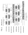
- The DFE operation of the 1-tap double-data rate configuration will now be described using data d1, d2 and d3 of
Fig.2 . - In the following, the data rate period is assumed to be T, with the half-rate clock period being 2T (in 10 Gbps communication, the data rate period T= 100 ps and the half rate clock period 2T= 200 ps).
- To the received data d2 influenced by ISI, is added a decision feedback signal, corresponding to an odd sampling data d1 multiplied by a tap gain (α), to generate a DFE-equalized even added signal:

- This DFE-equalized waveform is correctly sampled at an even half-rate clock to yield an even sampling data d2 with a period of 2T.
- This DFE equalized waveform is correctly sampled at an even half-rate clock to generate even sampling data d2 with the period of 2T.
- To remove ISI on an odd sampling data d3 by the sampling data d2, the odd DFE decision feedback signal 116 (=α×d2), corresponding to d2 multiplied by the tap gain (α), is fed back to the
odd DFE adder 111. The odd DFEdecision feedback signal 116 is added in thisodd DFE adder 111 to the received signal d3 so that the signal d3 is DFE-equalized. - This negative feedback process is repeated to realize DFE equalization of the double data rate system.
- It should be noted that, since the double-data rate system samples data at a half-rate clock, the sampling data is of the period 2T equal to twice the data rate period T.
- As a result, one of two signals to be added in the DFE adder is a received signal of the sampling data period of 2T, while the other is a received signal of the data rate period T.
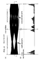
- The data waveform-equalized by DFE of
Fig.1 is only data at an odd or even sampling timing. Hence, the signals output from the DFE adders may be waveform equalized only at a rate of one per two data at each of the even and odd sides. As a result, there is produced a waveform which is an alternate repetition of waveform-equalized open eye data and non-waveform-equalized closed eye data, as shown inFig.4 . - Meghelli, Mounir; Rylov, Sergey; Bulzacchelli, John; Rhee, Woogeun, Rylyakov, Alexander; Ainspan, Herscel; Parker, Benjamin; Beakes, Michael; Chung, Aichin; Beukema, Troy; Pepeljugoski, Petar; Shan, Lei; Kwark, Young; Gowda, Sudhir; Friedman, Daniel, "A 10Gb/s 5-Tap DFE/ 4-Tap FFE Transceiver in 90-nm CMOS Technology", IEEE International Solid-State Circuits Conference, February 2006
- The entire disclosure of Non-Patent
Document 1 is incorporated herein by reference thereto. The following analyses are given by the present invention. - In serial communication, a clock signal is ordinarily not transmitted. Instead, a clock recovery circuit, abbreviated to 'CDR', which is configured to reproduce a clock signal from received data, is provided in a receiving side.
- In general, a double over-sampling CDR, in which a signal at a data center timing phase and a signal at an edge timing phase are detected and compared each other to adjust the phase of the reproduced clock, is now in wide spread use.
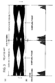
-
Fig.3 shows examples of full-rate DFE equalized eye pattern and edge distributions. From these edge distributions, the low-pass filtering function proper to the CDR extracts a distribution center to adjust a rising edge of a data sampling clock to a center position between the neighboring edges extracted to enable correct data sampling. - However, with the half-rate DFE, an eye opening may not be obtained on bits of before and after sides of an opening data sampled and edges are distributed over an entire time interval of the bit. As a result, there is elicited a problem that the center position between the edge positions cannot be correctly extracted and that a rising edge of the clock cannot be adjusted to a correct sampling phase position.
- Accordingly, it is an object of the present invention to provide a method and apparatus for phase adjustment of the reproduced clock in case of using the half-rate decision feedback equalization (half-rate DFE).
- It is another object of the present invention to provide a method and apparatus which may accomplish the above object and which may allow suppression of distributions of the reproduced clock to improve data sampling accuracy as well as to improve the communication quality.
- In accordance with one aspect of the present invention, there is provided a decision feedback equalization apparatus comprising an odd data receiving unit that receives an odd data sampling clock, an odd edge sampling clock and a DFE input signal and that includes a half-rate DFE equalization function, and an even data receiving unit that receives an even data sampling clock, an even edge sampling clock and the DFE input signal and that includes a half-rate DFE equalization function. The odd data receiving unit includes a data detection means and an edge detection means on a half-rate DFE equalized signal. The even data receiving unit include a data detection means and an edge detection means on a half-rate DFE equalized signal. The apparatus also comprises a pattern filter that receives a set of sampling data by the detection means and that detects a data pattern, three consecutive bits of which are 110 or 001. The pattern filter selects edge data based on a result of the detection so that edge data on the half-rate DFE equalized signal will be selected only on detection of the data pattern of 110 or 001. According to the present invention, clock recovery is executed on the basis of the output of the decision feedback equalizer.
- In accordance with another aspect of the present invention, there is provided a decision feedback equalization apparatus comprising an odd data receiving unit that receives an odd data sampling clock, an odd edge sampling clock and a DFE input signal and that includes a half-rate DFE equalization function, and an even data receiving unit that receives an even data sampling clock, an even edge sampling clock and the DFE input signal and that includes a half-rate DFE equalization function. The odd data receiving unit includes a data detection means, an edge detection means for detection on a half-rate DFE equalized signal, and an edge detection means for detection on a non-half-rate DFE equalized signal. The even data receiving unit includes a data detection means and an edge detection means for detection on a half-rate DFE equalized signal and an edge detection means for detection on a non-half-rate DFE equalized signal. The apparatus also comprises a pattern filter that includes means for receiving a set of sampling data by the detection means and for detecting a data pattern three consecutive bits of which are 110 or 001 and a data pattern three consecutive bits of which are 101 or 010. The means of the pattern filter selects edge data based on a result of the detection so that edge data on the half-rate DFE equalized signal will be selected on detection of the data pattern of 110 or 001 and so that edge data on the non-half-rate DFE equalized signal will be selected on detection of the data detection pattern of 101 or 010.
- According to the present invention, it is possible to adjust the phase of the recovered clock in case of using half-rate decision feedback equalization. According to the present invention, it is possible to suppress distributions of the recovered clock and to improve data sampling accuracy as well as the communication quality.
-
-
Fig.1 is a block diagram for illustrating DFE operation of a double data rate system. -
Fig.2 is a timing diagram for illustrating reception and DFE operation of the double data rate system. -
Fig.3 shows an example of eye patterns and edge distributions obtained on full-rate DFE. -
Fig.4 shows an example of an eye pattern and edge distributions obtained on half-rate DFE. -
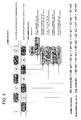
Fig.5 is a timing diagram for illustrating the operation of the half-rate DFE. -
Fig.6 is a graph for illustrating the quantity of the inter-symbol interference at each tap on a routine transmission line. -
Fig.7 is a schematic diagram showing the configuration of half-rate DFE and an edge detection block according to an exemplary embodiment of the present invention. -
Fig.8 is a timing diagram showing definitions of four-phase half-rate clocks, data and the edges. -
Fig.9 is a block diagram showing an arrangement of an edge detection unit of half-rate DFE according to an exemplary embodiment of the present invention. -
Fig.10 is a block diagram showing another arrangement of an edge detection unit of half-rate DFE according to an exemplary embodiment of the present invention. -
Fig.11 is a circuit diagram showing an edge detection unit of half-rate DFE according to an exemplary embodiment of the present invention. -
Fig.12 is a circuit diagram showing an example of a sampling unit of a differential configuration. -
Fig.13 is a circuit diagram showing an example of an n-tap DFE adder. -
Fig.14 is a schematic view showing an example of a phase comparator. -
Fig.15 is a diagram for illustrating certain examples of phase detection. -
Fig.16 is a diagram for illustrating the operation of a pattern filter. -
Fig.17 is a block diagram showing an arrangement of a pattern filter. - According to the present invention, there are provided an odd data receiving unit, an even data receiving unit, and a pattern filter. The odd data receiving which receives an odd data sampling clock, an odd edge sampling clock and a DFE input signal, includes a half-rate DFE equalization function. The even data receiving unit which receives an even data sampling clock, an even edge sampling clock and a DFE input signal, includes a half-rate DFE equalization function. The even data receiving unit and the odd data receiving unit each includes a data detection unit and an edge detection unit for data and edge detection on a half-rate DFE equalized signal. The pattern filter receives a set of sampling data by the detection units and includes a detection unit that detects a data pattern of three consecutive bits of 110 or 001 and that operates based on the detected result to select edge data on the half-rate DFE equalized signal only in case the detected pattern is the 110 or 001 pattern.
- According to the present invention, there are provided an odd data receiving unit, an even data receiving unit, and a pattern filter. The odd data receiving unit which receives an odd data sampling clock, an odd edge sampling clock and a DFE input signal, includes a half-rate DFE equalization function. The even data receiving unit which receives an even data sampling clock, an even edge sampling clock and a DFE input signal, includes a half-rate DFE equalization function. The even data receiving unit and the odd data receiving unit each includes a data detection unit and an edge detection unit for data and edge detection on a half-rate DFE equalized signal, and an edge detection unit for edge detection on a non-half-rate DFE equalized signal. The pattern filter receives a set of sampling data by the detection units and includes a detection unit that detects a data pattern of three consecutive bits of 110 or 001 and a data pattern of three consecutive bits of 101 or 010. The pattern filter operates based on the detected result to select edge data on the half-rate DFE equalized signal in case the data pattern is the 110 or 001 pattern as well as to select edge data on the non-half-rate DFE equalized signal in case the data pattern is the 101 or 010 pattern.
- According to the present invention, the pattern selector may be simplified in configuration by combining the pattern filter with the edge detection unit provided in the CDR. The pattern filter includes an EXOR operating mechanism for a detected data string of consecutive bits of the half-rate DFE equalized signal and a mechanism that selects the result of edge detection on the half-rate DFE equalized signal or the result of edge detection on the non-half-rate DFE equalized signal based on the result of the operation.
- According to the present invention, there is provided a mechanism that cancels the offset in the data sampling unit and the edge sampling unit of the half-rate DFE equalized signal to improve the error rate.
- According to the present invention, there is provided, in parallel with a data detection unit on the half-rate DFE equalized signal, an amplitude error sampling mechanism capable of adjusting a sampling threshold value to enable adaptive DFE equalization, thereby enabling adaptive DFE equalization in the receiving circuit.
- In the half-rate DFE, a decision feedback signal, optimized to the ISI, influencing given data, has a period twice the data rate (2T).
- The wide-range edge distribution of (B) of
Fig.4 may be attributed to the fact that the decision feedback signal with a 2-bit width is optimized for the first bit data, while it is not optimized for the second bit data. - The decision feedback signal, optimized for the first bit, is added to the waveform of the second bit, even though the value of the first bit differs from the second bit. Hence, the decision feedback signal, which is not proper, is added to the waveform of the second bit, thus closing one of the eye patterns.
- However, if it is supposed that the first bit data and the second bit data are influenced by the same influencing quantity of ISI, the two data are influenced similarly by the ISI, so that the two data are waveform-equalized in a proper manner. Under this supposed state, the full-rate DFE, shown in
Fig.3 , and the half-rate DFE, are of the same edge distribution. In this case, the half-rate clock phase may correctly be adjusted by the CDR. Thus, by using only edge data of the timing that fulfills this supposition for the CDR, it is possible for the CDR to correctly adjust the phase even with half-rate DFE to lead to solution of the above-described problem. - This condition will now be described with reference to
Fig.5 and certain mathematical expressions. -
Fig.5 depicts a timing diagram for illustrating an example of the operation of the half-rate DFE for removing the influencing quantity of ISI for the trailing 5 bits, referred to below as 5-tap DFE. It is noted however that the present invention is not limited to the number of taps equal to 5. - The received data are separated into two parallel paths. The data at the sampling timing of these two paths are waveform-equalized by half-rate DFE. The two parallel paths are termed 'an odd data sampling path' and 'an even data sampling path' in the description to follow.
- In the example of
Fig.5 , the odd data sampling path samples a data string of d1, d3, d5 and so forth, while the even data sampling path' samples a data string of d2, d4, d6 and so forth. The odd and even data sampling paths sample the data alternately. - It is noted that attention is to be focused on the waveform of the data d6 following the half-rate DFE of on each data sampling path. The signal level of the data d6 on the even data sampling path is expressed by the equation (I), while that of the same data d6 on the odd data sampling path is expressed by the equation (II).
- The sampling data d6 for half-rate DFE:

- The non-sampling data d6 for half-rate DFE:

- Referring to
Fig.5 , the meaning of variables wn of the equations (I) and (II), where n denotes an integer, is as follows: - w0: a DFE tap coefficient for a main tap bit (d6);
- w1: a DFE tap coefficient for the trailing first bit (d5);
- w2: a DFE tap coefficient for the trailing second bit (d4)
- wn: a DFE tap coefficient for the trailing n'th bit.
- In order for the non-sampling data signal of the equation (11) to be correctly equalized by DFE, the signal must be equal in signal level to the following signal for full-rate DFE:
- Sampling data d6 for full-rate DFE:

- Thus, under conditions where the equation (II) is equal to the equation (III), the waveform obtained with the half-rate DFE is equivalent to that obtained with the full-rate DFE. That is, under those conditions, the edges of the same timing may be extracted with the half-rate DFE as with the full-rate DFE.
- The conditions where the equation (II) is equal to the equation (III) include:
- (a) d4= d5, d3 =d4, d2= d3, d1= d2, d0= d1, d(-1)= d0; and
- (b) w1= w2= w3= ... w5= 0.
- The condition (b) is excluded because it means that DFE tap coefficients are all zero and hence that equalization is not used. As a result, the condition (a) represents the condition under which the correct edge that is desirably used may be obtained.
- This condition (a) is rewritten to

- Thus, the condition under which the same edge timing may be obtained with the half-rate DFE as with full-rate DFE is that the same data occurs in succession before occurrence of data transition.
- From the above consideration, data before d6 are preferably the same data for all time. However, such indicates that the same data are transmitted for all time. The data transmission of this sort may, of course, not be entitled to data communication.
- It should be noted however that wn, where n is 0, 1, 2 and so forth, are coefficients for correcting for an amount of ISI. These coefficients are determined by the amount of ISI on trailing side bits.
- In the routine backplane communication transmission line, such as FR4, the amount of the ISI on the trailing side bits tend to decrease gradually, as shown in
Fig.6 . - In particular, the first backward ISI amount w1 is appreciably larger than the second and the following ISI amount w2, w3 and so forth. In general, the tendency of wl>> w2, w3, w4 and so forth is outstanding.
- In short, the difference at the influencing quantity at the first backward ISI (influencing quantity w1), that is the absolute value |d5-d4|, plays a decisive role in the difference between the equations (II) and (III).
- As a result, it is practically possible to detect an edge position for the half-rate DFE at substantially the same position as that for the full-rate DFE if d5 and d4, which are 2-bit data directly previous to the sampling data, are equal to each other.
- Thus, if the edge is to be detected from the waveform after passage through the half-rate DFE stage, only such data transitions in which data directly before the edge and data two bits before the edge are the same, more specifically, in which the data sequence is of a pattern of "0→0→1" or "1→1→0", need to be detected by a pattern filter and used as edge data for the CDR. That is, doing so detects an edge timing similar to that in case of the full-rate DFE. It should be noted that, in the above discussions, the transmission of binary signals of "0" and "1" is presupposed.
- The processing of filtering by the pattern filter, as proposed by the present invention, enables detection of the edge similar to that detected with the full-rate DFE. However, another problem connected with a deteriorated jitter tolerance characteristic of a CDR may be incurred.
- This is due to negligence of 010 and 101 patterns, other than 001 and 110, in connection with transitions of the previous data of 01 and 10, by the data pattern filter. About one-half of edges thus cannot be used for phase adjustment by the CDR in case of communication of random data.
- Further, in generally used 8B10B encoding, the patterns of 01 alternations are present continually. Hence, edge detection is not possible with the above pattern filter, such that edges of the 010 and 101 patterns cannot be discounted.
- To eliminate this problem, the present invention proposes detecting the edges of data transitions from 010 and 101 from a waveform not equalized by half-rate DFE.
- The eye patterns of the waveforms, received before DFE, are closed. The frequency components of patterns of "01" alternations are substantially constant, and hence the ISI is small. The edge variations are small, such that filtering may sufficiently be achieved with a low-pass filter (LPF) ordinarily used as the CDR function.
- The edges of 010 and 101 data and those of 110 and 110 data are received simultaneously by parallel paths. However, there is produced a difference in delay depending on whether or not the data have been passed through the DFE circuit.
- Hence, the edge path for 010 data and for 101 data may cancel the signal delay difference by transmitting the data through a adder of zero DFE coefficient or by having delay included into the signal.
- It should be noted however that no data can be transmitted if data transmitted is perpetually alternation data of 1010..., as with 001 data or 110 data. For this reason, data is filtered by a pattern field of a 3-bit pattern, as a more realistic solution.
- The results of scrutiny on many standard boards indicate that edge variations can be suppressed with this 3-bit filter.
- It is seen from above that, if, in the double data rate receiving system, employing the half-rate clock, a half-rate DFE configuration is used, clock recovery is made possible even with the use of half-rate DFE, as in the case of using the full-rate DFE, by
- (1) using the results of sampling of the half-rate DFE equalized waveform for edge data of a pattern of 110 or a pattern of 001, and
- (2) using the results of sampling of the non-DFE equalized waveform for edge data of a pattern of 101 or a pattern of 010.
- The result is suppression of distribution of the recovered clock and improved accuracy in data sampling and in communication quality (bit error rate).
-
Fig.7 is a schematic view showing a configuration of an edge detection block, employing half-rate DFE, according to an exemplary embodiment of the present invention. Referring toFig.7 , aninput signal 700 is interleave-sampled in an odddata receiving unit 710 and an evendata receiving unit 720, each at a half clock rate. For sampling the input signal, two pairs of differential half-rate clocks, each with a phase offset of 90 degrees (four-phase half-rate clocks), as shown inFig.8 , are used. The input signal is subjected to double over-sampling at even data timing, odd data timing and at edge timings. - Referring to
Fig.8 , the odd data timing clock is clk0,
the odd edge timing clock is clk90, with a phase shift of 90 degrees from clk0,
the even data timing clock is clk180, with a phase shift of 180 degrees from clk0, and
the even edge timing clock is clk270, with a phase shift of 270 degrees from clk0. - The odd
data receiving unit 710 and the evendata receiving unit 720 are each provided with a mechanism for sampling the half-rate DFE equalized waveform at a data timing and at an edge timing, and a mechanism for sampling the non-half-rate DFE equalized waveform at an edge timing. - That is, the odd
data receiving unit 710 - .samplers the half-rate DFE equalized waveform at a data timing, using the clock clk0, to output the result as a
data decision data 711, and - · samples both the half-rate DFE equalized waveform and the non-half-rate DFE equalized waveform, at an edge timing, using the clock clk90, to output the result as
edge decision data - In similar manner, the even
data receiving unit 720 - · samples the half-rate DFE equalized waveform at a data timing, with the clock clk180, to output the result as a
data decision data 721, and - · samples both the half-rate DFE equalized waveform and the non-half-rate DFE equalized waveform, at an edge timing, using the clock clk270, to output the result as
edge decision data data receiving unit 710 combines a result of processing of the DFE equalizedwaveform 727 by the evendata receiving unit 720 with a result of processing of the DFE equalized waveform by the odddata receiving unit 710 to generate a decision feedback signal. The result of processing of the DFE equalizedwaveform 727 by the evendata receiving unit 720 is a tap gain output at an odd stage, as later described, while the result of processing of the DFE equalized waveform by the odddata receiving unit 710 is a tap gain output at an even stage, also as later described. The evendata receiving unit 720 combines the result of processing of the DFE equalizedwaveform 726 by the odddata receiving unit 710 with the result of processing of the DFE equalized waveform by the odddata receiving unit 710 to generate a decision feedback signal. The result of processing of the DFE equalizedwaveform processing 726 by the odd data receiving unit is ea tap gain output at an odd stage, as later described, while the result of processing of the DFE equalized waveform by the odddata receiving unit 710 is a tap gain output at an even stage, also as later described. - A
pattern filter 730 which receiving the above sampling data, selects, out of two sorts of the edge decision data (712 and 713; 722 and 723), sampled at odd and even edge timings, one of two sets of the edge timing data, depending on a data pattern of three consecutive bits, obtained from thedata decision data Edge decision data data decision data phase comparator 740 of the CDR for use for a data reproducing operation by the CDR. -
Fig.9 shows an example of an arrangement of the odddata receiving unit 710 ofFig.7 . The evendata receiving unit 720 ofFig.7 is symmetrical with respect to the arrangement of the odddata receiving unit 710. If the odd-even relationship is interchanged, the clock clk0 (180) is interchanged with the clock clk180 (0) and the clock clk90(270) is interchanged with the clock clk270 (90), the result is that thedata receiving units - The
input signal 700 is branched to the odddata receiving unit 710 and to the evendata receiving unit 720 so as to be then delivered to a DFE equalizedwaveform processing unit 900 and to a non-DFE equalizedwaveform processing unit 901 provided in each of the twodata receiving units - In the DFE equalized
waveform processing unit 900, aDFE adder 911 adds an input signal 100 and a decision feedback signal 916 together to output a DFE equalizedsignal 917. - The DFE equalized
signal 917 is sampled with clk0 by adata sampling unit 912, while being sampled with clk90 by anedge sampling unit 922. - The data decision data, sampled by the
data sampling unit 912, are negatively fed back via a set of latches 913 and a set of tap gains 915 as a feedback decision signal 916 for use for DFE processing by theDFE adder 911. Outputs of the odd stages of the tap gains 915-1, 915-3 and so forth in the odddata receiving unit 710 are delivered to associated odd adders 914-1, 914-3 and so forth of the even data receiving unit 720 (726 inFig.7 ), respectively. Those outputs of the odd stage tap gains are then added to outputs of even stage tap gains 915-2, 915-4 and so forth of the evendata receiving unit 720 to generate a decision feedback signal 918 which is then fed back to theDFE adder 911. Outputs of odd stage tap gains 915-1, 915-3 and so forth in the evendata receiving unit 720 are delivered to associated odd adders 914-1, 914-3 and so forth of the odd data receiving unit 710 (727 inFig.7 ), respectively so as to be then added to outputs of the even stage tap gains 915-2, 915-4 and so forth of the odddata receiving unit 710 to generate a decision feedback signal 918 which is then fed back to theDFE adder 911. - The tap gain 915 is a gain stage corresponding to wn of the equation (I), where n denotes a natural number. After passing through the set of the latches, the data decision data are output as odd
data decision data 711 to thepattern filter 730. Although thedata decision data 711 is output from the last latch of the set of the latches 913, it does not matter from which latch the data is branched and output to the pattern filter. - The edge decision data, sampled by the
edge sampling unit 922, is then delay-adjusted by a set of latches 923 so as to be output as the odd half-rate DFE equalizededge decision data 712 to thepattern filter 730. - In the non-DFE equalized
waveform processing unit 901, theinput signal 700 is delayed by delay adjustment 931 in an amount equivalent to the delay of theDFE adder 911. Anedge sampling unit 932 samples the edge decision data of the non-DFE equalized waveform with the clock clk90 of the same timing as the sampling timing of theedge sampling unit 922. - In
Fig.9 , there is shown an instance of delay adjustment 931 in which delay is adjusted using a dummy adder of the same configuration as theDFE adder 911 with one of input signals being a zero. - An output of the
edge sampling unit 932 is delay-adjusted by a set of latches 933, in the same way as the edge decision data is delay-adjusted by the set of latches 923. The so delay-adjusted output of the edge sampling unit is output to thepattern filter 730. It should be noted however that delay adjustment is made at thedata receiving units pattern filter 730 to discriminate time-domain data obtained on sampling thedata decision data 711 and that obtained on sampling theedge decision data -
Fig.9 shows an example in which decision feedback signals of all tap outputs of DFE are added by the DFE adders 914 to form the decision feedback signal 916 before delivery to theDFE adder 911. However, the present invention is not limited to this configuration. It does not matter which configuration is used provided that decision feedback signals of all taps are added at the output of theDFE adder 911 such as by directly summing the decision feedback signal of each tap at each DFE adder. - The waveform-processed data, thus generated, are output to the
pattern filter 730 to select edge decision data. -
Fig.10 shows a configuration of a front end of half-rate DFE provided with an offset canceling mechanism in case the sampling path and the sampling unit, needed for adjusting the DFE equalization coefficients, are arranged in a differential configuration. - Referring to
Fig.10 , a sampling path for sampling the half-rate DFE equalized waveform by an amplitudeerror sampling unit 942 is provided in parallel with thedata sampling unit 912 ofFig.9 . The amplitudeerror sampling unit 942 samples the result of comparison of an error decision reference potential 948 (Vref) on the half-rate DFE equalizedsignal 917 at a timing corresponding to clk0, as in thedata sampling unit 912. - The amplitude
error sampling unit 942 adjusts the delay in its output using e.g. a set of latches 943, as in thedata sampling unit 912. The output of the amplitude error sampling unit is delivered to a demultiplexer (DEMUX) 750, as is thedata decision data 711. - In the present invention, the sampling units may be of a single-ended configuration or of a differential configuration. In case of the differential configuration, there is a possibility that the
sampling units sampling units - In particular, in a transmission line having a large attenuation amount, in need of DFE equalization, an eye opening is small even after DFE equalization, thus presenting a problem at the time of the sampling.
- Thus, the sampling units (the data sampling unit, edge sampling unit and the amplitude error sampling unit) may each be provided with an offset correction mechanism to improve the bit error rate (BER).
-
Fig.11 shows an example of a differential flip-flop of the sampling unit.Fig.12 shows an example of an offset canceling mechanism for the differential flip-flop. - Referring to
Fig.11 , a differential input 1201 (in, inb) is delivered to a differential transistor pair (1221, 1222) of amaster latch 1202. - Clocks clk1205 and clk1206 form a differential clock pair. When a
transistor 1229 is turned on by clkb1205, an input is accepted, that is, the differential transistor pair (1221, 1222) is activated. When atransistor 1230 is turned on by clk1206, the signal so accepted is latched. Simultaneously, the latched signal is delivered to a differential transistor pair (1225, 1226) of aslave latch 1203. - When a
transistor 1232 is turned on, again by clkb1205, the signal accepted by the slave latch is latched. The so latched signal is delivered as adifferential output 1204 to thelatches - In the present Example, a differential latch with a single output (single-ended output) may also be used.
- Among the mechanisms for canceling the offset of the differential signal, there is one that cancels the offset within the differential flip-flop, or one that has a pre-stage circuit that generates offset for the differential signal.
Fig.12 shows an example of the latter mechanism. - Referring to
Fig.12 , a differential input is delivered to two differential pairs (1320, 1321) and (1322, 1323), the drain terminals of which are connected in common. Thetransistors transistors 1321 and 1322 are also equal in size to each other. The ratio of driving capabilities of thetransistors 1320 and 1321 is set to M:1, while that of thetransistors - The source terminals of the differential transistor pair (1320, 1321) are connected in common to a variable
current source 1310, while the source terminals of the differential transistor pair (1322, 1323) are connected to a variablecurrent source 1312. - The current amounts of the variable
current sources amount control signals - The ratio of current amounts of the variable
current sources differential output 1304. - By providing the above offset canceling mechanism in the
sampling units - In the illustrative arrangement, shown in
Fig.9 , decision feedback signals of all of the DFE tap outputs are added by the adder 914, before being supplied to theDFE adder 911, to constiture the decision feedback signal 916. However, the present invention is not limited to this configuration. It does not matter which configuration is used provided that decision feedback signals of all taps are added at the output of theDFE adder 911 such as by directly summing the decision feedback signals of the respective taps at the respective DFE adders. -
Fig.13 shows an example of directly adding the decision feedback signals of the respective taps by theDFE adder 911. Referring toFig.13 , a signal at adifferential input 1401 is supplied to a differential amplifier circuit of the initial stage made up of acurrent source 1410, a differential pair (1420, 1421) andload resistors 1424. A firstdecision feedback signal 1441, a seconddecision feedback signal 1442 and so forth up to an n'thdecision feedback signal 1443 are negatively fed back to adifferential output 1404. -
Fig.13 shows an example in which the decision feedback signal is differential. The firstdecision feedback signal 1441 is differentially delivered to the gates of a differential transistor pair (1422, 1423), the sources of which are connected in common and connected to a first variablecurrent source 1411 and the drains of which are connected to thedifferential output 1404. In similar manner, the n'thdecision feedback signal 1443 is differentially delivered to the gates of a differential transistor pair (1426, 1427), the sources of which are connected in common and connected to the n'th variablecurrent source 1413 and the drains of which are connected to thedifferential output 1404. Sign adjustment of the respective decision feedback signals is by any of suitable routine techniques (known techniques), although such technique is not shown inFig.13 . - The tap gain for each decision signals may be generated by controlling the first, second and n'th variable
current sources current control signals - In the present example, common mode control by common mode
negative feedback 1402 is carried out for thedifferential output 1404. - The waveform-processed data, thus generated, is delivered to the
pattern filter 730 where edge decision data is selected. - It is seen from above that, from the eye openings of every two bits, shown in
Fig.4 , data decision data and edge decision data may be obtained from the half-rate DFE equalized waveform, while edge decision data may be obtained from the non-half rate DFE decision data, in accordance with an interleaving system. - The configuration of the
pattern filter 730, which generates the edge timing of the same timing as that obtained with full-rate DFE from the half-rate DFE equalized data and from non-half rate DFE decision data, will now be described. - In case the data decision data string is of the 110 or 001 pattern, the data transition timing of the half rate DFE equalized data and that of the non-half rate DFE decision data become approximately equal to the data transition timing of the full-rate DFE equalized data.
- In case the data decision data string is of the 101 or 010 pattern, the data transition timing of the non-half rate DFE equalized data becomes approximately equal to the data transition timing of the full-rate DFE equalized data.
- In case this 3-bit pattern is to be filtered, a commonplace logic may be used. However, a 3-bit pattern filter has a wide area.
- Thus, the
pattern filter 730 effects pattern filtering of former two of the three bits and an edge detection means of thephase comparator 740 is used in combination to effect pattern filtering of three bits of 110 and 001 as well as 101 and 010 to reduce the pattern filter size. - The circuit configuration of the pattern filter of the present example, and the method for operating the same, will now be described. A generally used double rate over-sampling CDR includes the
customary phase comparator 740 for comparing a signal phase with a clock phase to detect data transition (edge) needed for clock recovery, and thus has the function of detecting an edge timing. -
Fig.14 shows an example of thephase comparator 740. - The
phase comparator 740 performs - an exclusive-OR (EXOR) operation of an odd data and an odd edge,
- an exclusive-OR (EXOR) operation of an odd edge and an even data,
- an exclusive-OR (EXOR) operation of an even data and an even edge,
- an exclusive-OR (EXOR) operation of an even edge and an odd data,
to adjust the phase of the recovered clock. -
Fig.15 shows examples of phase detection by the phase detector ofFig.13 . The edge timing in data transition from 0 to 1 is such that, in the signal state of (A) ofFig.15 , an up-signal = 1 and a down-signal = 0, as a result of the EXOR operation. ACDR logic 750 then exercises control to shift the clock phase towards the up-side. - In the signal state of (B) of
Fig.15 , the up-signal = 0 and the down-signal = 1. TheCDR logic 750 then exercises control to shift the clock phase towards the down-side. - If data shift is from 0 to 0, that is, there is no data transition, as in (C) of
Fig.15 , the up-signal = 0 and the down-signal = 0. In this case, no adjustment is made of the clock phase. - That is, a mechanism for detecting the presence or non-presence of data transition (edge) for phase adjustment of the reproduced clock is equipped in the CDR.
- This edge detection means may be used in place of pattern filtering of latter two bits of the three-bit pattern filter.
- In case of using the
phase comparator 740, it is unnecessary to filter a data string in thepattern filter 730 insofar as the transitions of the second andthird bits third bits - Thus, with the pattern filter, the result of the exclusive-OR (EXOR) operation on the former two bits (00, 11) is 0, insofar as detection of 001 and 110 patterns is concerned, while the result of the EXOR operation on the former two bits (01, 10) is 1, insofar as detection of 101 and 010 patterns is concerned
- It is sufficient if the result of edge detection with the DFE equalized waveform or that with the non-DFE equalized waveform is selected depending on the result of the EXOR operations.
-
Fig.16 summarizes the operation of the present Example. - Since all of the edge data are used, it is necessary to use both the 'odd data - even data' and 'even data - odd data' in the case of the double data rate system. It is therefore necessary to keep one bit of data in the pattern filter.
-
Fig.17 shows an example configuration of the pattern filter. It should be noted that a configuration other than the configuration ofFig.17 may be used provided that the configuration used allows filtering of the pattern proposed by the present invention. Referring toFig.17 , to thepattern filter 730 are delivered the odddata decision data 711, evendata decision data 721, half-rate DFE equalized oddedge decision data 712, even edgedecision data 722, odd edge decision data of the non-halfrate DFE waveform 713 and the evenedge decision data 723. - A flip-
flop 1810 adjusts the timing of a set of input data. - An even data (D2) 1821 and an odd data (D3) 1822 are EXORed by an
EXOR 1830. When the result of the operation indicates 1, aselector 1832 selects the odd half-rate DFE equalizededge decision data 712 and, when the result indicates 0, theselector 1832 selects the odd non-half-rate DFEedge decision data 713. - In similar manner, an odd data (D3) 1822 and an even data (D4) 1823 are EXORed by an
EXOR 1831. When the result of the operation indicates 1, aselector 1833 selects the even half-rate DFE equalizededge decision data 722 and, when the result indicates 0, theselector 1833 selects the even non-half-rate DFE equalizededge decision data 723. - As a result, an
edge data 1824 and aneven edge data 1825, filtered with 00 and 01 and with 01 and 10, are produced. - The timing of
data edges flop 1811. The timing adjusted data are output to thephase comparator 740 of the CDR shown inFig.15 . - The ensuing operation is as described above, that is, if there is transition at the next data, the CDR exploits the data and, if there is no transition, the CDR discounts it. Hence, a targeted 3-bit pattern filter of 001 and 110 as well as 101 and 010 may be constructed on the whole.
- By the above-described operation of the
pattern filter 730 and thephase comparator 740, it is possible to correctly select the half-rate DFE equalized edge decision data and the non-half-rate DFE equalized edge decision data to output the so selected data to the CDR logic. - The present Example thus provides, in a double data rate receiving system that uses a half-rate clock, a method for edge extraction in which clock recovery similar to that with the full-rate DFE may be achieved even though the half-rate DFE configuration is used. This is made possible by using the result of sampling of the half-rate DFE equalized waveform for a 001 pattern and a 110 pattern, and by using the result of sampling of the non-half-rate DFE equalized waveform for a 101 pattern and for a 010 pattern. Correct adjustment of the recovered clock leads to improved data sampling accuracy and to the improved bit error rate.
- Among the examples of practical use of the present invention, there are network equipment, such as servers or routers, and semiconductor devices used for storages.
- The disclosure of the aforementioned
Non-Patent Document 1 is incorporated by reference herein. The particular exemplary embodiments or examples may be modified or adjusted within the gamut of the entire disclosure of the present invention, inclusive of claims, based on the fundamental technical concept of the invention. Further, variegated combinations or selection of elements disclosed herein may be made within the framework of the claims. That is, the present invention may encompass various modifications or corrections that may occur to those skilled in the art in accordance with the within the gamut of the entire disclosure of the present invention, inclusive of claim and the technical concept of the present invention.
It should be noted that other objects, features and aspects of the present invention will become apparent in the entire disclosure and that modifications may be done without departing the gist and scope of the present invention as disclosed herein and claimed as appended herewith.
Also it should be noted that any combination of the disclosed and/or claimed elements, matters and/or items may fall under the modifications aforementioned.
According to an exemplary embodiment there is provided an apparatus including an odd data receiving unit (710) that receives an input signal, an even data receiving unit (720) that receives the input signal, and a pattern filter (730). The odd data receiving unit (710) samples a half-rate DFE equalized signal with an odd data timing clock to output data decision data (711). The odd data receiving unit (710) also samples both the half-rate DFE equalized waveform and a non-half-rate DFE equalized signal with an odd edge timing clock having the phase shifted by 90 degrees from the odd data timing clock to output resulting edge decision data (712, 713). The even data receiving unit (720) samples the half-rate DFE equalized waveform with an even data timing clock having the phase shifted by 180 degrees from the odd data timing clock to output data decision data (721). The even data receiving unit (720) also samples both the half-rate DFE equalized waveform and the non-half-rate DFE equalized waveform with an even edge timing clock having the phase shifted by 90 degrees from the even data timing clock to output resulting edge decision data (722, 723). The pattern filter (730) selects one of the edge decision data sampled at the odd edge timing and at the even edge timing in response to the value of a data pattern of three consecutive bits (110 or 001) obtained from the data decision data sampled at the odd and even data timings (Fig.7 ).
Claims (14)
- An apparatus for decision feedback equalization comprising:an odd data receiving unit that receives an odd data sampling clock, an odd edge sampling clock and a DFE input signal and that includes a half-rate DFE equalization function;an even data receiving unit that receives an even data sampling clock, an even edge sampling clock and the DFE input signal and that includes a half-rate DFE equalization function,the odd data receiving unit and the even data receiving unit each including a data detection means and an edge detection means that respectively perform data and edge detection on the half-rate DFE equalized signal; anda pattern filter that receives a set of sampling data by the detection means and that detects a data pattern, three consecutive bits of which are 110 or 001, the pattern filter, based on a result of the detection, selecting edge data on the half-rate DFE equalized signal when the data pattern of 110 or 001 is detected.
- A decision feedback equalization apparatus comprising:an odd data receiving unit that receives an odd data sampling clock, an odd edge sampling clock and a DFE input signal and that includes a half-rate DFE equalization function;an even data receiving unit that receives an even data sampling clock, an even edge sampling clock and the DFE input signal and that includes a half-rate DFE equalization function,the odd data receiving unit and the even data receiving unit each including: a data detection means and edge detection means that respectively, perform data and edge detection on a half-rate DFE equalized signal; and an edge detection means that performs edge detection on a non-half-rate DFE equalized signal; anda pattern filter that receives a set of sampling data by the detection means, the pattern filter detecting a data pattern, three consecutive bits of which are 110 or 001 and a data pattern, three consecutive bits of which are 101 or 010,the pattern filter, based on a result of the detection, selecting edge data detected on the half-rate DFE equalized signal, when the data pattern of 110 or 001 is detected, and selecting edge data detected on the non-half-rate DFE equalized signal when the data pattern of 101 or 010 is detected.
- The apparatus according to claim 1 or 2, wherein
the odd data receiving unit implements the half-rate DFE equalization function using a decision feedback signal in the odd data receiving unit and a decision feedback signal in the even data receiving unit; and wherein
the even data receiving unit implements the half-rate DFE equalization function using a decision feedback signal in the even data receiving unit and a decision feedback signal in the odd data receiving unit. - The apparatus according to any one of claims 1 to 3, wherein
the pattern filter includes:an exclusive-OR operation means executing an exclusive-OR operation on a detected string of consecutive data of the half-rate DFE equalized signal; anda selector that selects a result of edge detection on the half-rate DFE equalized signal or a result of edge detection on the non-half-rate DFE equalized signal, based on a result of the exclusive-OR operation executed by the exclusive-OR operation means. - The apparatus according to any one of claims 1 to 3, further comprising:a circuit that cancels offset at least one of the data detection means and edge detection means.
- The apparatus according to claim 1, wherein one or each of the odd data receiving unit and the even data receiving unit includes:an amplitude error sampling means arranged in parallel with the data detection means for data detection on the half-rate DFE equalized signal, the amplitude error sampling means having an adjustable sampling threshold value.
- An apparatus for decision feedback equalization comprising:an odd data receiving unit that receives an input signal;an even data receiving unit that receive the input signal; anda pattern filter that receives respective sampling data sampled by the odd data receiving unit and the even data receiving unit;the odd data receiving unit sampling a half-rate DFE equalized signal with an odd data timing clock and sampling both of the half-rate DFE equalized signal and a non-half-rate DFE equalized signal with an odd edge timing clock,the even data receiving unit sampling a half-rate DFE equalized signal with an even data timing clock and sampling both of the half-rate DFE equalized signal and the non-half-rate DFE equalized signal with an even edge timing clock,the pattern filter selecting, as one of the edge decision data sampled at the odd edge timing and at the even edge timing, one of the half-rate DFE equalized signal and the non-half-rate DFE equalized signal, in response to the value of a data pattern of three consecutive bits obtained from data decision data sampled at the odd and even data timings.
- The apparatus according to claim 7, wherein the odd data receiving unit and the even data receiving unit each include:a DFE equalized waveform processing unit receiving an input signal; anda non-DFE equalized waveform processing unit, also receiving the input signal, whereinthe DFE equalized waveform processing unit includes:a DFE adder that adds the input signal and a decision feedback signal to output a DFE equalized signal;a data sampling unit that samples the DFE equalized signal with the odd data timing clock or the even data timing clock; andan edge sampling unit that samples the DFE equalized signal with the odd edge timing clock or the even edge timing clock,data decision data, obtained on sampling by the data sampling unit, being negatively fed back as a decision feedback signal via a set of latches and a set of tap gains for use by the DFE adder for DFE equalization,the data decision data being also output as data decision data to the pattern filter after passage through the set of latches,the edge decision data, sampled by the edge sampling unit, being delay-adjusted by the set of latches and output as odd or even half-rate equalized edge decision data to the pattern filter, and whereinthe non-DFE equalized waveform processing unit includesan edge sampling unit that delays the input signal by an amount corresponding to delay caused by the DFE adder of the DFE equalized waveform processing unit and that samples the edge decision data of the non-half-rate DFE equalized signal with a timing clock of the same timing as the sampling timing of the edge sampling unit of the DFE equalized waveform processing unit,an output of the edge sampling unit being delay-adjusted by a set of latches and supplied to the pattern filter.
- The apparatus according to claim 7 or 8, wherein
a decision feedback signal, obtained on combining together an output of a preset stage tap gain of the set of tap gains of the odd data receiving unit and an output of a preset stage tap gain of the set of tap gains of the even data receiving unit, is negatively fed back to the DFE adder of the DFE equalized waveform processing unit of the odd data receiving unit; and wherein
a decision feedback signal, obtained on combining together an output of a preset stage tap gain of the set of tap gains of the even data receiving unit and an output of a preset stage tap gain of the set of tap gains of the odd data receiving unit, is negatively fed back to the DFE adder of the DFE equalized waveform processing unit of the even data receiving unit. - The apparatus according to any one of claims 7 to 9, wherein
the pattern filter selects edge data on the half-rate DFE equalized signal in case the data pattern of three consecutive bits is 110 or 001. - The apparatus according to any one of claims 7 to 9, wherein
the pattern filter detects data patterns of three consecutive bits of 110 or 001 or data patterns of three consecutive bits of 101 or 010; and wherein
the pattern filter selects edge data on the half-rate DFE equalized signal on detection of the 110 or 001 data pattern and selects edge data on the non-half-rate DFE equalized signal on detection of the 110 or 001 data pattern. - A method for decision feedback equalization comprising:sampling a half-rate DFE equalized signal with an odd data timing clock to output data decision data, and sampling both the half-rate DFE equalized signal and a non-half-rate DFE equalized signal with an odd edge timing clock to output edge decision data; andsampling a half-rate DFE equalized signal with an even data timing clock to output data decision data, and sampling both the half-rate DFE equalized signal and the non-half-rate DFE equalized signal with an even edge timing clock to output edge decision data; andselecting, as one of the edge decision data sampled at the odd edge timing and at the even edge timing, one of the half-rate DFE equalized signal and the non-half-rate DFE equalized signal, in response to the value of a data pattern of three consecutive bits obtained from the data decision data sampled at the odd and even data timings.
- The method according to claim 12, comprising
the pattern filter selecting edge decision data on the half-rate DFE equalized signal in case the data pattern of three consecutive bits is 110 or 001. - The method according to claim 12, comprising
the pattern filter detecting, as the data pattern of three consecutive bits, a data pattern of 110 or 001 or a data pattern of 010 or 101; and
the pattern filter selecting, on detection of the data pattern of 110 or 001, the edge decision data on the half-rate DFE equalized signal and the pattern filter selecting, on detection of the data pattern of 101 or 010, the edge decision data on the non-half-rate DFE equalized signal.
Applications Claiming Priority (1)
| Application Number | Priority Date | Filing Date | Title |
|---|---|---|---|
| JP2008066222A JP4956840B2 (en) | 2008-03-14 | 2008-03-14 | Judgment feedback equalization apparatus and method |
Publications (2)
| Publication Number | Publication Date |
|---|---|
| EP2101455A2 true EP2101455A2 (en) | 2009-09-16 |
| EP2101455A3 EP2101455A3 (en) | 2017-05-31 |
Family
ID=40756408
Family Applications (1)
| Application Number | Title | Priority Date | Filing Date |
|---|---|---|---|
| EP09155188.7A Withdrawn EP2101455A3 (en) | 2008-03-14 | 2009-03-13 | Apparatus and Method for Decision Feedback Equalization |
Country Status (3)
| Country | Link |
|---|---|
| US (1) | US8325792B2 (en) |
| EP (1) | EP2101455A3 (en) |
| JP (1) | JP4956840B2 (en) |
Cited By (5)
| Publication number | Priority date | Publication date | Assignee | Title |
|---|---|---|---|---|
| CN102103847A (en) * | 2009-12-22 | 2011-06-22 | 瑞萨电子株式会社 | Clock data recovery circuit and data transmission device for display device and method thereof |
| US20140286389A1 (en) * | 1999-10-19 | 2014-09-25 | Rambus Inc. | Multiphase Receiver with Equalization Circuitry |
| CN106664672A (en) * | 2014-08-21 | 2017-05-10 | 高通股份有限公司 | Multi iq-path synchronization |
| CN107615724A (en) * | 2015-06-05 | 2018-01-19 | 德克萨斯仪器股份有限公司 | Apparatus for processing serial data streams |
| US10862667B2 (en) | 2018-09-18 | 2020-12-08 | Samsung Display Co., Ltd. | Efficient frequency detectors for clock and data recovery circuits |
Families Citing this family (41)
| Publication number | Priority date | Publication date | Assignee | Title |
|---|---|---|---|---|
| US8477833B2 (en) | 2009-02-06 | 2013-07-02 | International Business Machines Corporation | Circuits and methods for DFE with reduced area and power consumption |
| JP5556361B2 (en) * | 2010-05-19 | 2014-07-23 | 日本電気株式会社 | Equalizer and equalization method |
| US8619848B2 (en) * | 2010-11-19 | 2013-12-31 | Intel Corporation | Method, apparatus, and system to compensate inter-symbol interference |
| US8401065B2 (en) * | 2011-02-14 | 2013-03-19 | Fujitsu Limited | Clock recovery circuit for receiver using decision feedback equalizer |
| US9191245B2 (en) * | 2011-03-08 | 2015-11-17 | Tektronix, Inc. | Methods and systems for providing optimum decision feedback equalization of high-speed serial data links |
| KR20130043559A (en) * | 2011-10-20 | 2013-04-30 | 삼성전자주식회사 | Equalizer, receiver circuit having the same and equalizer method |
| JP5937229B2 (en) * | 2011-12-21 | 2016-06-22 | インテル コーポレイション | Low power high speed digital receiver |
| WO2013137911A1 (en) * | 2012-03-16 | 2013-09-19 | Song Sanquan | Apparatus and system for switching equalization |
| JP6221274B2 (en) | 2012-05-14 | 2017-11-01 | 株式会社リコー | Data receiving apparatus and data communication system |
| US8729923B2 (en) * | 2012-08-29 | 2014-05-20 | Sandisk Technologies Inc. | Majority vote circuit |
| WO2014084894A1 (en) * | 2012-11-29 | 2014-06-05 | Massachusetts Institute Of Technology | Devices and techniques for integrated optical data communication |
| US9397868B1 (en) | 2012-12-11 | 2016-07-19 | Rambus Inc. | Split-path equalizer and related methods, devices and systems |
| CN104052508B (en) * | 2013-03-12 | 2018-06-01 | 马维尔国际贸易有限公司 | High-speed serial data receiver framework with double error comparators |
| US9367385B2 (en) | 2013-03-12 | 2016-06-14 | Marvell World Trade Ltd. | High speed serial data receiver architecture with dual error comparators |
| US8976855B2 (en) * | 2013-03-14 | 2015-03-10 | Intel Corporation | Power and area efficient receiver equalization architecture with relaxed DFE timing constraint |
| JP6032081B2 (en) * | 2013-03-22 | 2016-11-24 | 富士通株式会社 | Reception circuit and semiconductor integrated circuit |
| JP6079388B2 (en) | 2013-04-03 | 2017-02-15 | 富士通株式会社 | Reception circuit and control method thereof |
| US9165597B2 (en) | 2013-06-28 | 2015-10-20 | Seagate Technology Llc | Time-multiplexed single input single output (SISO) data recovery channel |
| US9674008B2 (en) * | 2013-10-31 | 2017-06-06 | Samsung Display Co., Ltd. | Body-biased slicer design for predictive decision feedback equalizers |
| JP6294691B2 (en) * | 2014-02-07 | 2018-03-14 | ルネサスエレクトロニクス株式会社 | Semiconductor device |
| JP2015192200A (en) | 2014-03-27 | 2015-11-02 | 富士通株式会社 | Receiver circuit |
| US9674025B2 (en) * | 2014-07-01 | 2017-06-06 | International Business Machines Corporation | 4-level pulse amplitude modulation transmitter architectures utilizing quadrature clock phases |
| EP2975813B1 (en) * | 2014-07-18 | 2018-12-26 | Tektronix, Inc. | Methods and systems for providing optimum decision feedback equalization of high-speed serial data links |
| JP6497069B2 (en) * | 2014-12-25 | 2019-04-10 | 富士通株式会社 | Decision feedback equalization circuit |
| US10341145B2 (en) * | 2015-03-03 | 2019-07-02 | Intel Corporation | Low power high speed receiver with reduced decision feedback equalizer samplers |
| US9699006B1 (en) * | 2015-12-14 | 2017-07-04 | Fujitsu Limited | Sign-based adaptive control with automatically-selected filter patterns |
| JP6597295B2 (en) * | 2015-12-25 | 2019-10-30 | 富士通株式会社 | Receiver and control method thereof |
| EP3477869B1 (en) * | 2016-06-24 | 2020-11-04 | Socionext Inc. | Equalization circuit, reception circuit and integrated circuit device |
| US20180006847A1 (en) * | 2016-06-30 | 2018-01-04 | Wenyan Vivian Jia | Sampler circuit with current injection for pre-amplification |
| US10637692B2 (en) * | 2017-09-26 | 2020-04-28 | Micron Technology, Inc. | Memory decision feedback equalizer |
| CN111684715B (en) | 2018-02-08 | 2023-05-02 | 株式会社索思未来 | Amplifying circuit, adding circuit, receiving circuit and integrated circuit |
| JP2020155859A (en) | 2019-03-19 | 2020-09-24 | キオクシア株式会社 | Semiconductor integrated circuits and receivers |
| CN111786669B (en) * | 2019-04-04 | 2023-09-12 | 智原微电子(苏州)有限公司 | Apparatus for adaptive control of decision feedback equalizer |
| TWI690178B (en) * | 2019-05-30 | 2020-04-01 | 瑞昱半導體股份有限公司 | Equalizer circuit |
| KR102711854B1 (en) * | 2020-08-18 | 2024-09-30 | 삼성전자주식회사 | Receiver circuit performing adaptive equalization and system including the same |
| CN114374375B (en) * | 2021-04-08 | 2025-03-07 | 中国科学院微电子研究所 | A decision feedback equalizer and PAM-4 receiver |
| US12244683B2 (en) * | 2022-09-19 | 2025-03-04 | Apple Inc. | Serial data receiver with even/odd mismatch compensation |
| CN115955425B (en) * | 2022-12-20 | 2025-05-23 | 裕太微(上海)电子有限公司 | A detection system for vehicle-mounted Ethernet link synchronization signal |
| CN116155664B (en) * | 2023-02-24 | 2025-09-23 | 上海安路信息科技股份有限公司 | DFE tap adaptive acquisition method and device based on clock phase shift |
| KR102674447B1 (en) * | 2023-03-30 | 2024-06-13 | 한국전자기술연구원 | Decision feedback equalizer circuit for high-speed receiver using serializer and method of driving the same |
| CN119127745A (en) * | 2024-07-31 | 2024-12-13 | 上海兆芯集成电路股份有限公司 | Decision Feedback Equalizer for Double Data Rate Memory |
Citations (1)
| Publication number | Priority date | Publication date | Assignee | Title |
|---|---|---|---|---|
| JP2008066222A (en) | 2006-09-11 | 2008-03-21 | Matsushita Electric Ind Co Ltd | High pressure discharge lamp |
Family Cites Families (20)
| Publication number | Priority date | Publication date | Assignee | Title |
|---|---|---|---|---|
| US7124221B1 (en) * | 1999-10-19 | 2006-10-17 | Rambus Inc. | Low latency multi-level communication interface |
| US7317756B2 (en) * | 2001-12-06 | 2008-01-08 | Pulse-Link, Inc. | Ultra-wideband communication apparatus and methods |
| US7805083B2 (en) * | 2003-04-28 | 2010-09-28 | Alcatel-Lucent Usa Inc. | Method and apparatus for data recovery in an optical transmission system |
| US7443913B2 (en) * | 2004-02-12 | 2008-10-28 | Texas Instruments Incorporated | High speed decision feedback equalizer |
| US7574146B2 (en) * | 2004-07-09 | 2009-08-11 | Infinera Corporation | Pattern-dependent error counts for use in correcting operational parameters in an optical receiver |
| US20060109940A1 (en) * | 2004-11-22 | 2006-05-25 | Troy Beukema | Timing bias compensation for a data receiver with decision-feedback equalizer |
| EP2367330B1 (en) * | 2005-01-20 | 2017-08-09 | Rambus Inc. | High-speed signaling systems with adaptable pre-emphasis and equalization |
| JP4888393B2 (en) * | 2005-09-28 | 2012-02-29 | 日本電気株式会社 | Clock regeneration apparatus and method |
| US7668238B1 (en) * | 2005-12-12 | 2010-02-23 | Xilinx, Inc. | Method and apparatus for a high speed decision feedback equalizer |
| US7616686B2 (en) * | 2006-02-17 | 2009-11-10 | Agere Systems Inc. | Method and apparatus for generating one or more clock signals for a decision-feedback equalizer using DFE detected data |
| US7924912B1 (en) * | 2006-11-01 | 2011-04-12 | Xilinx, Inc. | Method and apparatus for a unified signaling decision feedback equalizer |
| US7715474B2 (en) * | 2007-02-07 | 2010-05-11 | International Business Machines Corporation | Decision feedback equalizer (DFE) architecture |
| US7936812B2 (en) * | 2007-07-02 | 2011-05-03 | Micron Technology, Inc. | Fractional-rate decision feedback equalization useful in a data transmission system |
| US7792187B2 (en) * | 2007-08-31 | 2010-09-07 | International Business Machines Corporation | Multi-tap decision feedback equalizer (DFE) architecture eliminating critical timing path for higher-speed operation |
| US7944963B2 (en) * | 2007-12-28 | 2011-05-17 | International Business Machines Corporation | Method and apparatus for jitter compensation in receiver circuits using nonlinear dynamic phase shifting technique based on bit history pattern |
| US8085841B2 (en) * | 2008-04-02 | 2011-12-27 | International Business Machines Corporation | Sampled current-integrating decision feedback equalizer and method |
| US8126045B2 (en) * | 2008-08-29 | 2012-02-28 | International Business Machines Corporation | System and method for latency reduction in speculative decision feedback equalizers |
| US8369470B2 (en) * | 2008-11-25 | 2013-02-05 | Agere Systems, LLC | Methods and apparatus for adapting one or more equalization parameters by reducing group delay spread |
| US8442106B2 (en) * | 2009-12-14 | 2013-05-14 | Lsi Corporation | Floating-tap decision feedback equalizer for communication channels with severe reflection |
| US8942319B2 (en) * | 2010-04-08 | 2015-01-27 | Rambus Inc. | Partial response equalizer and related method |
-
2008
- 2008-03-14 JP JP2008066222A patent/JP4956840B2/en active Active
-
2009
- 2009-03-13 EP EP09155188.7A patent/EP2101455A3/en not_active Withdrawn
- 2009-03-16 US US12/404,714 patent/US8325792B2/en active Active
Patent Citations (1)
| Publication number | Priority date | Publication date | Assignee | Title |
|---|---|---|---|---|
| JP2008066222A (en) | 2006-09-11 | 2008-03-21 | Matsushita Electric Ind Co Ltd | High pressure discharge lamp |
Cited By (13)
| Publication number | Priority date | Publication date | Assignee | Title |
|---|---|---|---|---|
| US9998305B2 (en) | 1999-10-19 | 2018-06-12 | Rambus Inc. | Multi-PAM output driver with distortion compensation |
| US20140286389A1 (en) * | 1999-10-19 | 2014-09-25 | Rambus Inc. | Multiphase Receiver with Equalization Circuitry |
| US9544169B2 (en) * | 1999-10-19 | 2017-01-10 | Rambus Inc. | Multiphase receiver with equalization circuitry |
| CN102103847B (en) * | 2009-12-22 | 2014-10-22 | 瑞萨电子株式会社 | Clock data recovery circuit, data transfer device for display device, and data transfer method for display device |
| CN102103847A (en) * | 2009-12-22 | 2011-06-22 | 瑞萨电子株式会社 | Clock data recovery circuit and data transmission device for display device and method thereof |
| CN106664672A (en) * | 2014-08-21 | 2017-05-10 | 高通股份有限公司 | Multi iq-path synchronization |
| CN106664672B (en) * | 2014-08-21 | 2019-11-15 | 高通股份有限公司 | Multi-IQ Path Synchronization |
| CN107615724A (en) * | 2015-06-05 | 2018-01-19 | 德克萨斯仪器股份有限公司 | Apparatus for processing serial data streams |
| EP3332523A4 (en) * | 2015-06-05 | 2018-10-10 | Texas Instruments Incorporated | Apparatus for processing a serial data stream |
| CN107615724B (en) * | 2015-06-05 | 2021-06-01 | 德克萨斯仪器股份有限公司 | Apparatus for processing serial data streams |
| US10862667B2 (en) | 2018-09-18 | 2020-12-08 | Samsung Display Co., Ltd. | Efficient frequency detectors for clock and data recovery circuits |
| US11206124B2 (en) | 2018-09-18 | 2021-12-21 | Samsung Display Co., Ltd. | Efficient frequency detectors for clock and data recovery circuits |
| US11711199B2 (en) | 2018-09-18 | 2023-07-25 | Samsung Display Co., Ltd. | Efficient frequency detectors for clock and data recovery circuits |
Also Published As
| Publication number | Publication date |
|---|---|
| US20090232196A1 (en) | 2009-09-17 |
| JP2009225018A (en) | 2009-10-01 |
| JP4956840B2 (en) | 2012-06-20 |
| EP2101455A3 (en) | 2017-05-31 |
| US8325792B2 (en) | 2012-12-04 |
Similar Documents
| Publication | Publication Date | Title |
|---|---|---|
| US8325792B2 (en) | Apparatus and method for decision feedback equalization | |
| KR102252008B1 (en) | Multi-tap decision feed-forward equalizer with precursor and postcursor taps | |
| US9455848B1 (en) | DFE-skewed CDR circuit | |
| US8699559B2 (en) | Decision feedback equalization scheme with minimum correction delay | |
| US7616686B2 (en) | Method and apparatus for generating one or more clock signals for a decision-feedback equalizer using DFE detected data | |
| US7996584B2 (en) | Programmable cable with deskew and performance analysis circuits | |
| US7277516B2 (en) | Adaptive equalization system for a signal receiver | |
| US8467440B2 (en) | Compensated phase detector for generating one or more clock signals using DFE detected data in a receiver | |
| US9438450B1 (en) | Receiver and associated control method | |
| US12074737B2 (en) | SerDes receiver with optimized CDR pulse shaping | |
| US9288087B2 (en) | Data receiver circuit and method of adaptively controlling equalization coefficients using the same | |
| JP2007525061A (en) | Partial response receiver | |
| WO2009113462A1 (en) | Waveform equalization circuit and waveform equalization method | |
| US8509299B2 (en) | Decision feedback equalizer operable with multiple data rates | |
| US10069654B2 (en) | Methods to minimize the recovered clock jitter | |
| US9882795B1 (en) | Signal loss detector | |
| US9148316B2 (en) | Decision feedback equalizer | |
| TW202044806A (en) | Equalizer circuit | |
| KR102032370B1 (en) | Data recovery circuit and adaptive equalizer coefficients methods the same | |
| US20050254569A1 (en) | System and method for generating equalization coefficients | |
| US9130792B2 (en) | Closed-loop high-speed channel equalizer adaptation | |
| US10355889B1 (en) | Adaptive pattern filtering for clock and data recovery to minimize interaction with decision feedback equalization | |
| CN117459203A (en) | Retimer with limiter level adjustment | |
| US9300498B2 (en) | Decision-feedback analyzer and methods for operating the same | |
| WO2018217786A1 (en) | Multi-stage sampler with increased gain |
Legal Events
| Date | Code | Title | Description |
|---|---|---|---|
| PUAI | Public reference made under article 153(3) epc to a published international application that has entered the european phase |
Free format text: ORIGINAL CODE: 0009012 |
|
| AK | Designated contracting states |
Kind code of ref document: A2 Designated state(s): AT BE BG CH CY CZ DE DK EE ES FI FR GB GR HR HU IE IS IT LI LT LU LV MC MK MT NL NO PL PT RO SE SI SK TR |
|
| AX | Request for extension of the european patent |
Extension state: AL BA RS |
|
| RAP1 | Party data changed (applicant data changed or rights of an application transferred) |
Owner name: NEC CORPORATION Owner name: RENESAS ELECTRONICS CORPORATION |
|
| RAP1 | Party data changed (applicant data changed or rights of an application transferred) |
Owner name: RENESAS ELECTRONICS CORPORATION Owner name: NEC CORPORATION |
|
| PUAL | Search report despatched |
Free format text: ORIGINAL CODE: 0009013 |
|
| AK | Designated contracting states |
Kind code of ref document: A3 Designated state(s): AT BE BG CH CY CZ DE DK EE ES FI FR GB GR HR HU IE IS IT LI LT LU LV MC MK MT NL NO PL PT RO SE SI SK TR |
|
| AX | Request for extension of the european patent |
Extension state: AL BA RS |
|
| RIC1 | Information provided on ipc code assigned before grant |
Ipc: H04L 25/03 20060101AFI20170424BHEP Ipc: H04L 25/49 20060101ALI20170424BHEP |
|
| 17P | Request for examination filed |
Effective date: 20171130 |
|
| RBV | Designated contracting states (corrected) |
Designated state(s): AT BE BG CH CY CZ DE DK EE ES FI FR GB GR HR HU IE IS IT LI LT LU LV MC MK MT NL NO PL PT RO SE SI SK TR |
|
| AKX | Designation fees paid |
Designated state(s): DE GB |
|
| AXX | Extension fees paid |
Extension state: RS Extension state: AL Extension state: BA |
|
| 17Q | First examination report despatched |
Effective date: 20180226 |
|
| GRAP | Despatch of communication of intention to grant a patent |
Free format text: ORIGINAL CODE: EPIDOSNIGR1 |
|
| GRAJ | Information related to disapproval of communication of intention to grant by the applicant or resumption of examination proceedings by the epo deleted |
Free format text: ORIGINAL CODE: EPIDOSDIGR1 |
|
| GRAP | Despatch of communication of intention to grant a patent |
Free format text: ORIGINAL CODE: EPIDOSNIGR1 |
|
| INTG | Intention to grant announced |
Effective date: 20190524 |
|
| INTC | Intention to grant announced (deleted) | ||
| INTG | Intention to grant announced |
Effective date: 20190614 |
|
| STAA | Information on the status of an ep patent application or granted ep patent |
Free format text: STATUS: THE APPLICATION IS DEEMED TO BE WITHDRAWN |
|
| 18D | Application deemed to be withdrawn |
Effective date: 20191001 |