EP2099070A1 - Process for producing resistance change device - Google Patents
Process for producing resistance change device Download PDFInfo
- Publication number
- EP2099070A1 EP2099070A1 EP06834970A EP06834970A EP2099070A1 EP 2099070 A1 EP2099070 A1 EP 2099070A1 EP 06834970 A EP06834970 A EP 06834970A EP 06834970 A EP06834970 A EP 06834970A EP 2099070 A1 EP2099070 A1 EP 2099070A1
- Authority
- EP
- European Patent Office
- Prior art keywords
- film
- transition metal
- resistance change
- change element
- metal oxide
- Prior art date
- Legal status (The legal status is an assumption and is not a legal conclusion. Google has not performed a legal analysis and makes no representation as to the accuracy of the status listed.)
- Granted
Links
Images



Classifications
-
- H—ELECTRICITY
- H10—SEMICONDUCTOR DEVICES; ELECTRIC SOLID-STATE DEVICES NOT OTHERWISE PROVIDED FOR
- H10N—ELECTRIC SOLID-STATE DEVICES NOT OTHERWISE PROVIDED FOR
- H10N70/00—Solid-state devices having no potential barriers, and specially adapted for rectifying, amplifying, oscillating or switching
- H10N70/011—Manufacture or treatment of multistable switching devices
- H10N70/021—Formation of switching materials, e.g. deposition of layers
-
- H—ELECTRICITY
- H10—SEMICONDUCTOR DEVICES; ELECTRIC SOLID-STATE DEVICES NOT OTHERWISE PROVIDED FOR
- H10B—ELECTRONIC MEMORY DEVICES
- H10B63/00—Resistance change memory devices, e.g. resistive RAM [ReRAM] devices
- H10B63/30—Resistance change memory devices, e.g. resistive RAM [ReRAM] devices comprising selection components having three or more electrodes, e.g. transistors
-
- H—ELECTRICITY
- H10—SEMICONDUCTOR DEVICES; ELECTRIC SOLID-STATE DEVICES NOT OTHERWISE PROVIDED FOR
- H10N—ELECTRIC SOLID-STATE DEVICES NOT OTHERWISE PROVIDED FOR
- H10N70/00—Solid-state devices having no potential barriers, and specially adapted for rectifying, amplifying, oscillating or switching
- H10N70/011—Manufacture or treatment of multistable switching devices
- H10N70/061—Shaping switching materials
- H10N70/063—Shaping switching materials by etching of pre-deposited switching material layers, e.g. lithography
-
- H—ELECTRICITY
- H10—SEMICONDUCTOR DEVICES; ELECTRIC SOLID-STATE DEVICES NOT OTHERWISE PROVIDED FOR
- H10N—ELECTRIC SOLID-STATE DEVICES NOT OTHERWISE PROVIDED FOR
- H10N70/00—Solid-state devices having no potential barriers, and specially adapted for rectifying, amplifying, oscillating or switching
- H10N70/20—Multistable switching devices, e.g. memristors
-
- H—ELECTRICITY
- H10—SEMICONDUCTOR DEVICES; ELECTRIC SOLID-STATE DEVICES NOT OTHERWISE PROVIDED FOR
- H10N—ELECTRIC SOLID-STATE DEVICES NOT OTHERWISE PROVIDED FOR
- H10N70/00—Solid-state devices having no potential barriers, and specially adapted for rectifying, amplifying, oscillating or switching
- H10N70/801—Constructional details of multistable switching devices
-
- H—ELECTRICITY
- H10—SEMICONDUCTOR DEVICES; ELECTRIC SOLID-STATE DEVICES NOT OTHERWISE PROVIDED FOR
- H10N—ELECTRIC SOLID-STATE DEVICES NOT OTHERWISE PROVIDED FOR
- H10N70/00—Solid-state devices having no potential barriers, and specially adapted for rectifying, amplifying, oscillating or switching
- H10N70/801—Constructional details of multistable switching devices
- H10N70/821—Device geometry
- H10N70/826—Device geometry adapted for essentially vertical current flow, e.g. sandwich or pillar type devices
-
- H—ELECTRICITY
- H10—SEMICONDUCTOR DEVICES; ELECTRIC SOLID-STATE DEVICES NOT OTHERWISE PROVIDED FOR
- H10N—ELECTRIC SOLID-STATE DEVICES NOT OTHERWISE PROVIDED FOR
- H10N70/00—Solid-state devices having no potential barriers, and specially adapted for rectifying, amplifying, oscillating or switching
- H10N70/801—Constructional details of multistable switching devices
- H10N70/881—Switching materials
- H10N70/883—Oxides or nitrides
- H10N70/8833—Binary metal oxides, e.g. TaOx
-
- Y—GENERAL TAGGING OF NEW TECHNOLOGICAL DEVELOPMENTS; GENERAL TAGGING OF CROSS-SECTIONAL TECHNOLOGIES SPANNING OVER SEVERAL SECTIONS OF THE IPC; TECHNICAL SUBJECTS COVERED BY FORMER USPC CROSS-REFERENCE ART COLLECTIONS [XRACs] AND DIGESTS
- Y10—TECHNICAL SUBJECTS COVERED BY FORMER USPC
- Y10T—TECHNICAL SUBJECTS COVERED BY FORMER US CLASSIFICATION
- Y10T29/00—Metal working
- Y10T29/49—Method of mechanical manufacture
- Y10T29/49002—Electrical device making
- Y10T29/49082—Resistor making
- Y10T29/49099—Coating resistive material on a base
-
- Y—GENERAL TAGGING OF NEW TECHNOLOGICAL DEVELOPMENTS; GENERAL TAGGING OF CROSS-SECTIONAL TECHNOLOGIES SPANNING OVER SEVERAL SECTIONS OF THE IPC; TECHNICAL SUBJECTS COVERED BY FORMER USPC CROSS-REFERENCE ART COLLECTIONS [XRACs] AND DIGESTS
- Y10—TECHNICAL SUBJECTS COVERED BY FORMER USPC
- Y10T—TECHNICAL SUBJECTS COVERED BY FORMER US CLASSIFICATION
- Y10T29/00—Metal working
- Y10T29/49—Method of mechanical manufacture
- Y10T29/49002—Electrical device making
- Y10T29/49117—Conductor or circuit manufacturing
- Y10T29/49124—On flat or curved insulated base, e.g., printed circuit, etc.
-
- Y—GENERAL TAGGING OF NEW TECHNOLOGICAL DEVELOPMENTS; GENERAL TAGGING OF CROSS-SECTIONAL TECHNOLOGIES SPANNING OVER SEVERAL SECTIONS OF THE IPC; TECHNICAL SUBJECTS COVERED BY FORMER USPC CROSS-REFERENCE ART COLLECTIONS [XRACs] AND DIGESTS
- Y10—TECHNICAL SUBJECTS COVERED BY FORMER USPC
- Y10T—TECHNICAL SUBJECTS COVERED BY FORMER US CLASSIFICATION
- Y10T29/00—Metal working
- Y10T29/49—Method of mechanical manufacture
- Y10T29/49002—Electrical device making
- Y10T29/49117—Conductor or circuit manufacturing
- Y10T29/49124—On flat or curved insulated base, e.g., printed circuit, etc.
- Y10T29/49155—Manufacturing circuit on or in base
Definitions
- the present invention relates to a method of manufacturing a resistance change element storing data by utilizing change in a resistance value.
- ReRAM Resistive Random Access Memory
- a ReRAM data is stored by utilizing change in a resistance value of a resistance change element.
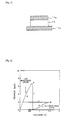
- the resistance change element is configured such that an NiO film (nickel oxide film) 12 or another transition metal oxide film is sandwiched in between a pair of electrodes 11a 11b made of Pt (platinum).
- a treatment applying a predetermined voltage to the resistance change element configured as such is carried out, it is possible to change the resistance value by controlling the current and voltage.
- Fig. 2 is a view showing the state change of the resistance change element by taking the horizontal axis as voltage and the vertical axis as current.
- the resistance change element transitions between a high resistance state and a low resistance state according to the current flowing through the inside of the resistance change element and the voltage applied thereto.
- the current flowing through the inside of the resistance change element increases as the applied voltage becomes higher, while the inclination of the curved line showing the relationship between the voltage and the current is relatively small.
- the applied voltage becomes equal to or higher than a specified voltage (as shown by b in Fig. 2 )
- the resistance value decreases rapidly (as shown by c in the Figure).
- the current increases rapidly.
- a limiter circuit for preventing rapid current increase is provided for the ReRAM so as to prevent a large current from flowing into the resistance change element.
- the inclination of the curved line showing the relationship between the voltage and the current is large.
- the resistance change element transitions to the high resistance state (as shown by f in the Figure), and the current decreases rapidly.
- the resistance change element transitions to the low resistance state when a voltage equal to or higher than a specified voltage is applied in the high resistance state, while the resistance change element transitions to the high resistance state when a current equal to or higher than a specified current is applied in the low resistance state.
- the resistance value in the low resistance state is approximately several kQ and the resistance value in the high resistance state is from approximately several tens k ⁇ to 1 M ⁇ . Note that, in general, the change from the high resistance state to the low resistance state is referred to as "set” and the change from the low resistance state to the high resistance state is referred to as "reset:".
- Patent Citation 1 describes a non-volatile memory having a resistance change element with the structure in which a film made of any of transition metal oxides such as NiO, TiO 2 , HfO, ZrO, ZnO, WO 3 , CoO, and Nb 2 O 5 is sandwiched in between a pair of electrodes.
- a conventional resistance change element needs to receive a current of several mA to 10 mA or more in order to transition from the low resistance state to the high resistance state.
- a current flowing through each cell is set to be equal to or less than 1 mA, the power consumption of a semiconductor storage device (IC) is so huge, but depending on its required memory capacity, that the commercialization thereof is difficult.
- An object of the present invention is to provide a method of manufacturing a resistance change element capable of reducing the amount of current per cell, as compared with the conventional one.
- a method of manufacturing a resistance change element includes forming a first noble metal film made of any one of a noble metal and a noble metal oxide above a semiconductor substrate, forming a transition metal film on the first noble metal film, forming a transition metal oxide film by oxidizing a surface of the transition metal film, and forming a second noble metal film made of any one of a noble metal and a noble metal oxide on the transition metal oxide film.
- the inventors of the present application and the like have carried out various experiments and studies with an intention to reduce the driving current of ReRAM.
- the driving current of a resistance change element can be reduced when an Ni (nickel) film is formed on the ground-side (negative polarity-side) electrode of the resistance change element and a transition metal oxide film (NiOx film) is formed by performing an oxidation treatment to the surface of the Ni film. It is not apparent why the driving current decreases when the Ni film is formed between the ground-side electrode and transition metal oxide film of the resistance change element.
- the film formed on the ground-side electrode may be formed of a transition metal other than Ni, for example, Ti (titanium), Co (cobalt), or Ta (tantalum).
- the transition metal oxide film is formed by oxidizing the surface of the transition metal. Accordingly, when the transition metal film is made of Ti, the transition metal oxide film is formed of TiO 2 . When the transition metal film is made of Co, the transition metal oxide film is formed of CoO. When the transition metal film is made of Ta, the transition metal oxide film is formed of Ta 2 O 5 .
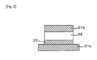
- Fig. 3 is a cross-sectional view showing a resistance change element according to an embodiment of the present invention.
- the resistance change element according to the present embodiment is configured by laminating, in the following order from the bottom thereof, a lower electrode (ground-side electrode) 21a made of Pt (platinum), a transition metal film 22 made of Ni (nickel), a transition metal oxide film 23 made of NiOx (nickel oxide film), and an upper electrode (positive polarity-side electrode) 21b made of Pt.
- x in NiOx is any positive number, and is preferably larger than 0 and less than 2 in order to obtain a preferable characteristic.
- the lower electrode 21a and the upper electrode 21b may be formed of a noble metal other than Pt, for example, Pd (palladium), Ru (ruthenium), or Ir (iridium), or an oxide thereof.
- the lower electrode 21a is formed of Pt.
- the transition metal film 22 is formed by sputtering Ni onto the lower electrode 21a. After that, the surface of the transition metal film 22 is oxidized in an oxidizing atmosphere to form the transition metal oxide film 23 made of NiOx. In this case, if the entire transition metal film 22 is oxidized, the effect of reducing a driving current cannot be obtained. Therefore, it is necessary to adjust a temperature and time of oxidation treatment so as to control the thickness of the remaining transition metal film 22.
- the thicknesses of the transition metal film and the transition metal oxide film after oxidation treatment are checked by the cross-sectional SEM (Scanning Electron Microscope) observation, the film crystallinity measurement, or the elemental analysis in the depth direction by using the XPS (X-ray Photoelectron Spectroscopy).
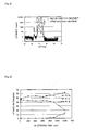
- Fig. 4 is a view showing the results of measuring a ample before oxidation treatment and a sample after oxidation treatment with the X-ray diffraction (XRD) by taking the horizontal axis as angle (20) and the vertical axis as intensity (count).
- the sample used for the measurement is such that a metal film (lower electrode) made of Pt is formed on a silicon substrate and an Ni film with the thickness of 60 nm is formed thereon by the sputtering method.
- the oxidation treatment is performed by heating at 400°C for 30 minutes in the oxidizing atmosphere.
- Fig. 5 is a view showing the results of performing the elemental analysis in the depth direction of the sample after oxidation treatment with the XPS by taking the horizontal axis as etching time and the vertical axis as atomic ratio.
- an Ar gas is used for the etching.
- the atomic ratio of oxygen is high when the etching time is 0 to 900 seconds, and when the etching time exceeds 900 seconds, the atomic ratio of oxygen decreases and the atomic ratio of Ni increases. This means that unoxidized Ni remains in the vicinity of the lower electrode.
- the thickness of the unoxidized Ni film is 10 nm.
- the inventors of the present application and the like formed a large number of resistance change elements, each having different thicknesses of the transition metal film (Ni film) 22 and the transition metal oxide film (NiOx film) 23, and checked characteristics thereof.
- Fig. 6 shows these results.
- the preferable resistance change characteristic is shown only when the thickness of the transition metal film (Ni film) is between 5 nm and 20 nm inclusive and the thickness of the transition metal oxide film (NiOx film) is between 5 nm and 65 nm inclusive (the range surrounded by the broken line in the Figure) and the preferable resistance change characteristic is not shown in a range other than that.
- the resistance value is excessively low if the thickness of the transition metal oxide film is less than 5 nm. As a result, the resistance value required in a high resistance state cannot be obtained. In addition, if the thickness of the transition metal oxide film exceeds 65 nm, the resistance value is excessively high. As a result, the resistance value required in a low resistance state cannot be obtained. Furthermore, if the thickness of the transition metal film is less than 5 nm, the effect of reducing the reset current cannot be sufficiently obtained.
- the thickness of the transition metal film exceeds 20 nm, it is presumable that the reaction between Pt and Ni develops to lead to an increase in unevenness on the surface of the NiOx film.
- Fig. 7 is a view showing the results of checking the condition in a case where the thickness of the Ni film after oxidation treatment is 5 nm or 10 nm by taking the horizontal axis as temperature of the oxidation treatment and the vertical axis as time of the oxidation treatment. It should be noted that the results of checking the condition when the Ni film disappears is also shown in Fig. 7 .
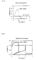
- Fig. 8 is a view showing the characteristic of the resistance change element formed according to a method of the present invention (hereinafter referred to as a practical example) by taking the horizontal axis as voltage and the vertical axis as current.
- Fig. 9 is a view showing the characteristic of a resistance change element (hereinafter referred to as a comparative example) with the structure shown in Fig. 1 .
- the set voltage is approximately 1.2 V and the reset current is approximately 0.8 mA, which are low.
- the set voltage is approximately 2 V and the reset current is approximately 20 mA, which are large.
- the transition metal film 22 may be formed of a transition metal other than Ni, for example, Ti (titanium), Co (cobalt), or Ta (tantalum).
- the transition metal oxide film 23 is formed by oxidizing the surface of the transition metal film 22. Accordingly, when the transition metal film 22 is made of Ti, the transition metal oxide film 23 is formed of TiO 2 . When the transition metal film 22 is made of Co, the transition metal oxide film 23 is formed of CoO. When the transition metal film 22 is made of Ta, the transition metal oxide film 23 is formed of Ta 2 O 5 film.
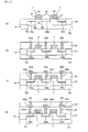
- Figs. 10 to 12 are cross-sectional views, each showing in the order of processes a method of manufacturing a ReRAM according to the embodiment of the present invention.
- a memory cell as well as an n-type transistor and a p-type transistor which constitute driving circuits (a write circuit, a read circuit and the like) are formed on a semiconductor substrate, but are not shown in the figures herein.
- an element isolation film 51 is formed in a predetermined region in a semiconductor substrate (silicon substrate) 50 by the well-known STI (Shallow Trench Isolation) method or the LOCOS (Local Oxidation of Silicon) method.
- the surface of the semiconductor substrate 50 is separated into multiple element regions by the resultant element isolation film 51.
- a p-type impurity such as boron (B) is introduced into an n-type transistor forming region (a memory cell region and an n-type transistor forming region of the driving circuit; hereinafter, the same) in the semiconductor substrate 50 to form a p-well 52.
- an n-type impurity such as phosphorus (P) is introduced into a p-type transistor forming region (a p-type transistor forming region of the driving circuit; hereinafter, the same) in the semiconductor substrate 50 to form an n-well (unillustrated).
- the surfaces of the p-well 52 and the n-well are thermally oxidized to form a gate insulating film 53.
- a polysilicon film is formed on the entire upper surface of the semiconductor substrate 50 by the CVD (Chemical Vapor Deposition) method.
- the resultant polysilicon film is patterned by the photolithography method and the etching method to form gate electrodes 54.
- the two gate electrodes 54 serving as word lines are disposed on one p-well 52 so as to be parallel to each other.
- an n-type impurity such as phosphorus (P) with low concentration is ion-implanted into the p-well 52 in the n-type transistor forming region, so that n-type low concentration impurity regions 56 are formed.
- a p-type impurity such as boron (B) with low concentration is ion-implanted into the n-well (unillustrated) in the p-type transistor forming region, so that p-type low concentration impurity regions (unillustrated) are formed.
- side walls 57 are formed on both sides of the gate electrode 54. These side walls 57 are formed such that an insulating film made of SiO 2 , SiN, or the like is formed on the entire upper surface of the semiconductor substrate 50 by the CVD method, and then the resultant insulating film is etched back to be left only on the both sides of the gate electrode 54.
- the gate electrode 54 and the side walls 57 as masks, an n-type impurity with high concentration is ion-implanted into the p-well 52 in the n-type transistor forming region, so that the n-type high concentration impurity regions 58a, 58b are formed.
- the high concentration impurity region 58a is an impurity region (drain) disposed between the gate electrode 54 and the element isolation film 51.
- the high concentration impurity region 58b is an impurity region (source) disposed between the two gate electrodes 54.
- a p-type impurity with high concentration is ion-implanted into the n-well (unillustrated) to from a p-type high concentration impurity region (unillustrated).
- the transistor T having a source and a drain with the LDD (Lightly Doped Drain) structure in each transistor forming region is formed.
- an SiO 2 film for example, is formed as a first interlayer insulating film 61 on the entire upper surface of the semiconductor substrate 50 by the CVD method.
- the transistor T is covered with the resultant interlayer insulating film 61.
- the surface of the first interlayer insulating film 61 is polished and planarized by the CMP (Chemical Mechanical Polishing) method.
- contact holes reaching the n-type high concentration impurity regions 58a, 58b in the n-type transistor forming region from the upper surface of the first interlayer insulating film 61 are formed.
- a TiN film (unillustrated) serving as a barrier metal is formed on the entire upper surface of the semiconductor substrate 50 by the sputtering method.
- a W film is formed on the TiN film by the sputtering method or the CVD method, while W is filled in the contact holes.
- the W film and the TiN film are polished by the CMP method until the first interlayer insulating film 61 is exposed.
- W plugs 62a, 62b made by being filled with W are formed in the contact holes.
- the W plug 62a is a plug connected to the high concentration impurity region 58a and the W plug 62b is a plug connected to the high concentration impurity region 58b.
- a conducting film formed of a metal such as aluminum or copper is formed on the first interlayer insulating film 61 and the W plugs 62a, 62b by the sputtering method.
- the resultant conducting film is patterned by the photolithography method and the etching method to form pad 63a and wiring 63b.
- the pad 63a is formed on the W plug 62a and is electrically connected to the W plug 62a.
- the wiring 63b passes on the plug 63b and is electrically connected to the W plug 63b.
- a second interlayer insulating film 65 made of SiO 2 is formed on the entire upper surface of the semiconductor substrate 50 by the CVD method. Subsequently, the surface of the resultant interlayer insulating film 65 is polished and planarized by the CMP method. Thereafter, by using the photolithography method and the etching method, contact holes, each reaching the pad 63a from the upper surface of the second interlayer insulating film 65, are formed. After that, a TiN film (unillustrated) serving as a barrier metal is formed on the entire upper surface of the semiconductor substrate 50 by the sputtering method.
- a W film is formed on the TiN film by the sputtering method or the CVD method, while W is filled in the contact holes.
- the W film and the TiN film are polished by the CMP method until the second interlayer insulating film 65 is exposed. In this manner, W plug 66 made by being filled with W is formed in the contact holes.
- a Ti or TiN film (unillustrated) is formed, with the thickness of, for example, 20 nm, on the second interlayer insulating film 65 and the W plug 66 by the sputtering method.
- This Ti or TiN film is not a must, but serves to improve the adhesiveness between the interlayer insulating film 65 and the lower electrode 67a as well as the electrical connectivity between the W plug 66 and the lower electrode 67a.
- a Pt film 67 serving as a lower electrode is formed with the thickness of, for example, 50 nm to 100 nm on the second interlayer insulating film 65 and the W plug 66 (on the Ti or TiN film).
- an Ni film 68 is formed with the thickness of, for example, 60 nm on the Pt film 67 by the sputtering method.
- a transition metal oxide film 69 made of NiOx is formed.
- the thickness of the Ni film 68 becomes approximately 10 nm.
- the oxidation of the Ni film 68 may be performed by the RTA (Rapid Thermal Anneal) method.
- a Pt film 70 serving as an upper electrode is formed with the thickness of, for example, 50 nm on the NiOx film 69.
- an antireflection film (unillustrated) made of TiN is formed on the Pt film 70 with the thickness of, for example, 50 nm.
- the antireflection film is formed in order to prevent light reflection in the next photolithography process. Therefore, it is only necessary that this antireflection film is formed if needed, and is not a must in the present invention.
- a resist film (unillustrated) having a predetermined shape is formed on the Pt film 70.
- the resultant resist film As a result, as shown in Fig. 12 (a) , formed is a resistance change element 71 having the structure in which the lower electrode 67a made of Pt, the transition metal film 68a made of Ni, the transition metal oxide film 69a made of NiOx, and the upper electrode 70a made of Pt are laminated.
- a third interlayer insulating film 72 made of SiO 2 is formed on the entire upper surface of the semiconductor substrate 50 by the CVD method.
- contact holes each reaching the upper electrode 70a of the resistance change element 71 from the upper surface of the third interlayer insulating film 72, are formed.
- a TiN film (unillustrated) serving as a barrier metal is formed on the entire upper surface of the semiconductor substrate 50.
- a W film is formed on the barrier metal by the sputtering method or the CVD method, and W is filled in the contact holes.
- the W film and the TiN film are polished by the CMP method until the third interlayer insulating film 72 is exposed. In this manner, a W plug 73 electrically connected to the upper electrode 70a of the resistance change element 71 is formed.
- a conducting film (unillustrated) having the laminated structure of TiN/Al/TiN/Ti, for example, is formed on the third interlayer insulating film 72 and the W plug 73.
- the conducting film is patterned by the photolithography method and the etching method to form, as shown in Fig. 12(c) , a wiring (bit line) 74. In this manner, the ReRAM is completed.
- the wiring 74, the gate electrode 54 of each transistor T, and the wiring 63b respectively are a bit line, a word line, and a ground line.
- the transistor T is turned on to apply a predetermined voltage to the resistance change element 71 through the wiring 74 (bit line) by setting the lower electrode 67a to a ground potential.
- the transistor T is turned on to apply a predetermined current to the resistance change element 71 through the wiring (bit line) 74 by setting the lower electrocte 67a to a ground potential.
- the transistor T is turned on to check a resistance between the wiring (bit line) 74 and the wiring 63b (ground line).
- the resistance change element 71 is configured of the lower electrode 67a made of Pt, the transition metal film 68a made of Ni, the transition metal oxide film 69a made of NiOx, and the upper electrode 70a made of Pt. Therefore, there is such an effect that a driving voltage is low and a driving current is small. In this manner, the ReRAM can be highly integrated to meet such demands that information apparatuses are further reduced in size and save power consumption while having higher functionality.
- the present embodiment has been described by using the example in which the present invention is applied to a stack-type ReRAM. However, the present invention is also applicable to a planer-type ReRAM.
Landscapes
- Engineering & Computer Science (AREA)
- Manufacturing & Machinery (AREA)
- Semiconductor Memories (AREA)
Abstract
Description
- The present invention relates to a method of manufacturing a resistance change element storing data by utilizing change in a resistance value.
- In recent years, further size reduction, lower power consumption and higher functionality have been demanded for information apparatuses such as computers. Along with these demands, there has also been a demand for non-volatile semiconductor memories that enable higher integration, operate at a higher speed, and retain stored data even when power is not supplied. As one of the next generation non-volatile semiconductor memories capable of meeting such demands, a resistance change memory (Resistive Random Access Memory: hereinafter referred to as "ReRAM") including a resistance change element has been developed (see, for example,
Non Patent Citations 1, 2). - In a ReRAM, data is stored by utilizing change in a resistance value of a resistance change element. As shown in
Fig. 1 , the resistance change element is configured such that an NiO film (nickel oxide film) 12 or another transition metal oxide film is sandwiched in between a pair ofelectrodes 11a -
Fig. 2 is a view showing the state change of the resistance change element by taking the horizontal axis as voltage and the vertical axis as current. As shown in thisFig. 2 , the resistance change element transitions between a high resistance state and a low resistance state according to the current flowing through the inside of the resistance change element and the voltage applied thereto. In the high resistance state, as shown by a in the Figure, the current flowing through the inside of the resistance change element increases as the applied voltage becomes higher, while the inclination of the curved line showing the relationship between the voltage and the current is relatively small. In contrast, when the applied voltage becomes equal to or higher than a specified voltage (as shown by b inFig. 2 ), the resistance value decreases rapidly (as shown by c in the Figure). As a result, the current increases rapidly. For this reason, a limiter circuit for preventing rapid current increase is provided for the ReRAM so as to prevent a large current from flowing into the resistance change element. - In the low resistance state, as shown by d in the Figure, the inclination of the curved line showing the relationship between the voltage and the current is large. When the current flowing into the resistance change element becomes a specified value (as shown by e in the Figure), the resistance change element transitions to the high resistance state (as shown by f in the Figure), and the current decreases rapidly.
- As described above, the resistance change element transitions to the low resistance state when a voltage equal to or higher than a specified voltage is applied in the high resistance state, while the resistance change element transitions to the high resistance state when a current equal to or higher than a specified current is applied in the low resistance state. The resistance value in the low resistance state is approximately several kQ and the resistance value in the high resistance state is from approximately several tens kΩ to 1 MΩ. Note that, in general, the change from the high resistance state to the low resistance state is referred to as "set" and the change from the low resistance state to the high resistance state is referred to as "reset:".
- Since the NiO film constituting the resistance change element is an oxide, the electrodes holding both sides of the NiO film is in an easily-oxidizable state. For this reason, the electrodes of the resistance change element are formed of a metal which is hardly oxidized. Specifically, the electrodes are formed of a noble metal such as Pt or Ir (iridium) .
Patent Citation 1 describes a non-volatile memory having a resistance change element with the structure in which a film made of any of transition metal oxides such as NiO, TiO2, HfO, ZrO, ZnO, WO3, CoO, and Nb2O5 is sandwiched in between a pair of electrodes. - The inventors of the present application and the like have found the following problem in a conventional ReRAM. Specifically, as shown in
Fig. 2 , a conventional resistance change element needs to receive a current of several mA to 10 mA or more in order to transition from the low resistance state to the high resistance state. On the other hand, unless a current flowing through each cell is set to be equal to or less than 1 mA, the power consumption of a semiconductor storage device (IC) is so huge, but depending on its required memory capacity, that the commercialization thereof is difficult. - Patent Citation 1: Japanese Laid-open Patent Application Publication No.
2006-140489 - Non Patent Citation 1: K. Kinoshita et al., "Bias polarity dependent data retention of resistive random access memory consisting of binary transition metal oxide", APPLIED PHYSICS LETTER 89, 103509 (2006)
- Non Patent Citation 2: S. Seo et al., "Reproducible resistance switching in polycrystalline NiO films", APPLIED PHYSICS LETTER Vol. 85, No. 23, 6 December 2004)
- An object of the present invention is to provide a method of manufacturing a resistance change element capable of reducing the amount of current per cell, as compared with the conventional one.
- According to an aspect of the present invention, a method of manufacturing a resistance change element is provided. The method includes forming a first noble metal film made of any one of a noble metal and a noble metal oxide above a semiconductor substrate, forming a transition metal film on the first noble metal film, forming a transition metal oxide film by oxidizing a surface of the transition metal film, and forming a second noble metal film made of any one of a noble metal and a noble metal oxide on the transition metal oxide film.
- The inventors of the present application and the like have carried out various experiments and studies with an intention to reduce the driving current of ReRAM. As a result, it has been found that the driving current of a resistance change element can be reduced when an Ni (nickel) film is formed on the ground-side (negative polarity-side) electrode of the resistance change element and a transition metal oxide film (NiOx film) is formed by performing an oxidation treatment to the surface of the Ni film. It is not apparent why the driving current decreases when the Ni film is formed between the ground-side electrode and transition metal oxide film of the resistance change element. However, it can be assumed that if there is no Ni film, the diffusion of elements from the noble metal electrode to the transition metal oxide film or the diffusion of oxygen from the transition metal oxide film to the noble metal electrode occurs to cause driving voltage to be higher and driving current to be larger, whereas if the Ni film is formed between the ground-side electrode and the transition metal oxide film, such a phenomenon does not occur.
- The film formed on the ground-side electrode may be formed of a transition metal other than Ni, for example, Ti (titanium), Co (cobalt), or Ta (tantalum). In the present invention, the transition metal oxide film is formed by oxidizing the surface of the transition metal. Accordingly, when the transition metal film is made of Ti, the transition metal oxide film is formed of TiO2. When the transition metal film is made of Co, the transition metal oxide film is formed of CoO. When the transition metal film is made of Ta, the transition metal oxide film is formed of Ta2O5.
-
- [
Fig. 1] Fig. 1 is a cross-sectional view showing a conventional resistance change element; - [
Fig. 2] Fig. 2 is a view showing an example of the state change of the resistance change element; - [
Fig. 3] Fig. 3 is a cross-sectional view showing a resistance change element according to an embodiment of the present invention; - [
Fig. 4] Fig. 4 is a view showing the results of measuring a sample before oxidation treatment and a sample after oxidation treatment with X-ray diffraction (XRD); - [
Fig. 5] Fig. 5 is a view showing the results of performing an elemental analysis in the depth direction of the sample after oxidation treatment with XPS; - [
Fig. 6] Fig. 6 is a view showing the results of checking the relationship between the thickness and characteristic of a transition metal film (Ni film) and transition metal oxide film (NiOx film); - [
Fig. 7] Fig. 7 is a view showing the results of checking the condition when the thickness of the Ni film after oxidation treatment is set to be 5 nm or 10 nm; - [
Fig. 8] Fig. 8 is a view showing the characteristic of the resistance change element according a practical example; - [
Fig. 9] Fig. 9 is a view showing the characteristic of a resistance change element according to a comparative example; - [
Fig. 10] Fig. 10 is cross-sectional view (No. 1) showing a method of manufacturing a ReRAM according to the embodiment of the present invention; - [
Fig. 11] Fig. 11 is cross-sectional view (No. 2) showing the method of manufacturing a ReRAM according to the embodiment of the present invention; and - [
Fig. 12] Fig. 12 is cross-sectional view (No. 3) showing the method of manufacturing a ReRAM according to the embodiment of the present invention. - Hereinafter, an embodiment of the present invention will be described with reference to the accompanying drawings.
-
Fig. 3 is a cross-sectional view showing a resistance change element according to an embodiment of the present invention. As shown in thisFig. 3 , the resistance change element according to the present embodiment is configured by laminating, in the following order from the bottom thereof, a lower electrode (ground-side electrode) 21a made of Pt (platinum), atransition metal film 22 made of Ni (nickel), a transitionmetal oxide film 23 made of NiOx (nickel oxide film), and an upper electrode (positive polarity-side electrode) 21b made of Pt. Here, x in NiOx is any positive number, and is preferably larger than 0 and less than 2 in order to obtain a preferable characteristic. - The
lower electrode 21a and the upper electrode 21b may be formed of a noble metal other than Pt, for example, Pd (palladium), Ru (ruthenium), or Ir (iridium), or an oxide thereof. In the present embodiment thelower electrode 21a is formed of Pt. Subsequently, thetransition metal film 22 is formed by sputtering Ni onto thelower electrode 21a. After that, the surface of thetransition metal film 22 is oxidized in an oxidizing atmosphere to form the transitionmetal oxide film 23 made of NiOx. In this case, if the entiretransition metal film 22 is oxidized, the effect of reducing a driving current cannot be obtained. Therefore, it is necessary to adjust a temperature and time of oxidation treatment so as to control the thickness of the remainingtransition metal film 22. For this reason, it is significant to check in advance the relationship between the temperature and time of oxidation treatment and the thickness of the remaining transition metal film. The thicknesses of the transition metal film and the transition metal oxide film after oxidation treatment are checked by the cross-sectional SEM (Scanning Electron Microscope) observation, the film crystallinity measurement, or the elemental analysis in the depth direction by using the XPS (X-ray Photoelectron Spectroscopy). -
Fig. 4 is a view showing the results of measuring a ample before oxidation treatment and a sample after oxidation treatment with the X-ray diffraction (XRD) by taking the horizontal axis as angle (20) and the vertical axis as intensity (count). It should be noted that the sample used for the measurement is such that a metal film (lower electrode) made of Pt is formed on a silicon substrate and an Ni film with the thickness of 60 nm is formed thereon by the sputtering method. In addition, the oxidation treatment is performed by heating at 400°C for 30 minutes in the oxidizing atmosphere. - As can be seen from
Fig. 4 , in the sample before oxidation treatment, only the peaks of Si (200), Pt (111), and Ni (111) are observed. However, in the sample after oxidation treatment, the peak of NiO (200) is also observed in addition to the peaks of Si (200), Pt (111), and Ni (111). From this result, it can be seen that an NiOx film is formed and the Ni film also remains after the oxidation treatment when the oxidation treatment is performed by heating at 400°C for 30 minutes. -
Fig. 5 is a view showing the results of performing the elemental analysis in the depth direction of the sample after oxidation treatment with the XPS by taking the horizontal axis as etching time and the vertical axis as atomic ratio. Here, an Ar gas is used for the etching. - It can be seen from this
Fig. 5 that the atomic ratio of oxygen is high when the etching time is 0 to 900 seconds, and when the etching time exceeds 900 seconds, the atomic ratio of oxygen decreases and the atomic ratio of Ni increases. This means that unoxidized Ni remains in the vicinity of the lower electrode. As a result obtained by observing the cross-section of the sample after oxidation treatment with the SEM, the thickness of the unoxidized Ni film is 10 nm. - Next, in the configuration shown in
Fig. 3 , the inventors of the present application and the like formed a large number of resistance change elements, each having different thicknesses of the transition metal film (Ni film) 22 and the transition metal oxide film (NiOx film) 23, and checked characteristics thereof.Fig. 6 shows these results. As shown in thisFig. 6 , the preferable resistance change characteristic is shown only when the thickness of the transition metal film (Ni film) is between 5 nm and 20 nm inclusive and the thickness of the transition metal oxide film (NiOx film) is between 5 nm and 65 nm inclusive (the range surrounded by the broken line in the Figure) and the preferable resistance change characteristic is not shown in a range other than that. That is, the resistance value is excessively low if the thickness of the transition metal oxide film is less than 5 nm. As a result, the resistance value required in a high resistance state cannot be obtained. In addition, if the thickness of the transition metal oxide film exceeds 65 nm, the resistance value is excessively high. As a result, the resistance value required in a low resistance state cannot be obtained. Furthermore, if the thickness of the transition metal film is less than 5 nm, the effect of reducing the reset current cannot be sufficiently obtained. - Although it is not apparent why the characteristic cannot be sufficiently obtained when the thickness of the transition metal film (Ni film) exceeds 20 nm, it is presumable that the reaction between Pt and Ni develops to lead to an increase in unevenness on the surface of the NiOx film.
-
Fig. 7 is a view showing the results of checking the condition in a case where the thickness of the Ni film after oxidation treatment is 5 nm or 10 nm by taking the horizontal axis as temperature of the oxidation treatment and the vertical axis as time of the oxidation treatment. It should be noted that the results of checking the condition when the Ni film disappears is also shown inFig. 7 . -
Fig. 8 is a view showing the characteristic of the resistance change element formed according to a method of the present invention (hereinafter referred to as a practical example) by taking the horizontal axis as voltage and the vertical axis as current.Fig. 9 is a view showing the characteristic of a resistance change element (hereinafter referred to as a comparative example) with the structure shown inFig. 1 . - As can be seen from
Fig. 8 , in the resistance change element according to the practical example formed according to a method of the present invention, the set voltage is approximately 1.2 V and the reset current is approximately 0.8 mA, which are low. In contrast, as can be seen fromFig. 9 , in the resistance change element according Lo the comparative example, the set voltage is approximately 2 V and the reset current is approximately 20 mA, which are large. - In
Fig. 3 , thetransition metal film 22 may be formed of a transition metal other than Ni, for example, Ti (titanium), Co (cobalt), or Ta (tantalum). In the present invention, the transitionmetal oxide film 23 is formed by oxidizing the surface of thetransition metal film 22. Accordingly, when thetransition metal film 22 is made of Ti, the transitionmetal oxide film 23 is formed of TiO2. When thetransition metal film 22 is made of Co, the transitionmetal oxide film 23 is formed of CoO. When thetransition metal film 22 is made of Ta, the transitionmetal oxide film 23 is formed of Ta2O5 film. -
Figs. 10 to 12 are cross-sectional views, each showing in the order of processes a method of manufacturing a ReRAM according to the embodiment of the present invention. In general, a memory cell as well as an n-type transistor and a p-type transistor which constitute driving circuits (a write circuit, a read circuit and the like) are formed on a semiconductor substrate, but are not shown in the figures herein. - Firstly, the process to form the structure shown in
Fig. 10(a) will be described. As shown inFig. 10(a) , anelement isolation film 51 is formed in a predetermined region in a semiconductor substrate (silicon substrate) 50 by the well-known STI (Shallow Trench Isolation) method or the LOCOS (Local Oxidation of Silicon) method. The surface of thesemiconductor substrate 50 is separated into multiple element regions by the resultantelement isolation film 51. - Next, a p-type impurity such as boron (B) is introduced into an n-type transistor forming region (a memory cell region and an n-type transistor forming region of the driving circuit; hereinafter, the same) in the
semiconductor substrate 50 to form a p-well 52. In addition, an n-type impurity such as phosphorus (P) is introduced into a p-type transistor forming region (a p-type transistor forming region of the driving circuit; hereinafter, the same) in thesemiconductor substrate 50 to form an n-well (unillustrated). - Subsequently, the surfaces of the p-well 52 and the n-well (unillustrated) are thermally oxidized to form a
gate insulating film 53. After that, a polysilicon film is formed on the entire upper surface of thesemiconductor substrate 50 by the CVD (Chemical Vapor Deposition) method. The resultant polysilicon film is patterned by the photolithography method and the etching method to formgate electrodes 54. At this time, as shown inFig. 10(a) , in the memory cell region, the twogate electrodes 54 serving as word lines are disposed on one p-well 52 so as to be parallel to each other. - Thereafter, using the
gate electrodes 54 as masks, an n-type impurity such as phosphorus (P) with low concentration is ion-implanted into the p-well 52 in the n-type transistor forming region, so that n-type lowconcentration impurity regions 56 are formed. Similarly, using thegate electrodes 54 as masks, a p-type impurity such as boron (B) with low concentration is ion-implanted into the n-well (unillustrated) in the p-type transistor forming region, so that p-type low concentration impurity regions (unillustrated) are formed. - Thereafter,
side walls 57 are formed on both sides of thegate electrode 54. Theseside walls 57 are formed such that an insulating film made of SiO2, SiN, or the like is formed on the entire upper surface of thesemiconductor substrate 50 by the CVD method, and then the resultant insulating film is etched back to be left only on the both sides of thegate electrode 54. - Thereafter, using the
gate electrode 54 and theside walls 57 as masks, an n-type impurity with high concentration is ion-implanted into the p-well 52 in the n-type transistor forming region, so that the n-type highconcentration impurity regions concentration impurity region 58a is an impurity region (drain) disposed between thegate electrode 54 and theelement isolation film 51. The highconcentration impurity region 58b is an impurity region (source) disposed between the twogate electrodes 54. - Similarly, using the gate electrode and side walls in the p-type transistor forming region as masks, a p-type impurity with high concentration is ion-implanted into the n-well (unillustrated) to from a p-type high concentration impurity region (unillustrated). In this manner, the transistor T having a source and a drain with the LDD (Lightly Doped Drain) structure in each transistor forming region is formed.
- Next, the process to form the structure shown in
Fig. 10(b) will be described. After the transistor T is formed by the process described above, an SiO2 film, for example, is formed as a firstinterlayer insulating film 61 on the entire upper surface of thesemiconductor substrate 50 by the CVD method. The transistor T is covered with the resultantinterlayer insulating film 61. After that, the surface of the firstinterlayer insulating film 61 is polished and planarized by the CMP (Chemical Mechanical Polishing) method. - Subsequently, by using the photolithography method and the etching method, contact holes reaching the n-type high
concentration impurity regions interlayer insulating film 61 are formed. After that, a TiN film (unillustrated) serving as a barrier metal is formed on the entire upper surface of thesemiconductor substrate 50 by the sputtering method. Thereafter, a W film is formed on the TiN film by the sputtering method or the CVD method, while W is filled in the contact holes. After that, the W film and the TiN film are polished by the CMP method until the firstinterlayer insulating film 61 is exposed. In this manner, W plugs 62a, 62b made by being filled with W are formed in the contact holes. Here, theW plug 62a is a plug connected to the highconcentration impurity region 58a and theW plug 62b is a plug connected to the highconcentration impurity region 58b. - Next, the process to form the structure shown in
Fig. 10 (c) will be described. After the W plugs 62a, 62b are formed by the process described above, a conducting film formed of a metal such as aluminum or copper is formed on the firstinterlayer insulating film 61 and the W plugs 62a, 62b by the sputtering method. Subsequently, the resultant conducting film is patterned by the photolithography method and the etching method to formpad 63a andwiring 63b. Thepad 63a is formed on theW plug 62a and is electrically connected to theW plug 62a. In addition, thewiring 63b passes on theplug 63b and is electrically connected to theW plug 63b. - Next, the process to form the structure shown in
Fig. 10(d) will be described. After thepad 63a and thewiring 63b are formed by the process described above, a secondinterlayer insulating film 65 made of SiO2 is formed on the entire upper surface of thesemiconductor substrate 50 by the CVD method. Subsequently, the surface of the resultantinterlayer insulating film 65 is polished and planarized by the CMP method. Thereafter, by using the photolithography method and the etching method, contact holes, each reaching thepad 63a from the upper surface of the secondinterlayer insulating film 65, are formed. After that, a TiN film (unillustrated) serving as a barrier metal is formed on the entire upper surface of thesemiconductor substrate 50 by the sputtering method. Thereafter, a W film is formed on the TiN film by the sputtering method or the CVD method, while W is filled in the contact holes. After that, the W film and the TiN film are polished by the CMP method until the secondinterlayer insulating film 65 is exposed. In this manner, W plug 66 made by being filled with W is formed in the contact holes. - Next, the process to form the structure shown in
Figs. 11(a) to 11(c) will be described. After theW plug 66 is formed by the process described above, a Ti or TiN film (unillustrated) is formed, with the thickness of, for example, 20 nm, on the secondinterlayer insulating film 65 and the W plug 66 by the sputtering method. This Ti or TiN film is not a must, but serves to improve the adhesiveness between the interlayer insulatingfilm 65 and thelower electrode 67a as well as the electrical connectivity between theW plug 66 and thelower electrode 67a. - Subsequently, as shown in
Fig. 11(a) , by the sputtering method, aPt film 67 serving as a lower electrode is formed with the thickness of, for example, 50 nm to 100 nm on the secondinterlayer insulating film 65 and the W plug 66 (on the Ti or TiN film). Thereafter, anNi film 68 is formed with the thickness of, for example, 60 nm on thePt film 67 by the sputtering method. After that, thissemiconductor substrate 50 is placed in an electric furnace to be subjected to the thermal treatment at the temperature of 400°C for 30 minutes in the oxidizing atmosphere. This results in oxidation of the surface of theNi film 68. As a result, as shown inFig. 11(b) , a transitionmetal oxide film 69 made of NiOx is formed. With this oxidation treatment, the thickness of theNi film 68 becomes approximately 10 nm. It should be noted that the oxidation of the Ni film 68 (transition metal film) may be performed by the RTA (Rapid Thermal Anneal) method. - Thereafter, as shown in
Fig. 11(c) , by the sputtering method, aPt film 70 serving as an upper electrode is formed with the thickness of, for example, 50 nm on theNiOx film 69. In addition, an antireflection film (unillustrated) made of TiN is formed on thePt film 70 with the thickness of, for example, 50 nm. The antireflection film is formed in order to prevent light reflection in the next photolithography process. Therefore, it is only necessary that this antireflection film is formed if needed, and is not a must in the present invention. - Next, the process to form the structure shown in
Figs. 12(a) to 12(c) will be described. After thePt film 70 is formed by the process described above, a resist film (unillustrated) having a predetermined shape is formed on thePt film 70. By using the resultant resist film as a mask, thePt film 70, theNiOx film 69, theNi film 68, and thePt film 67 are etched. As a result, as shown inFig. 12 (a) , formed is aresistance change element 71 having the structure in which thelower electrode 67a made of Pt, thetransition metal film 68a made of Ni, the transitionmetal oxide film 69a made of NiOx, and theupper electrode 70a made of Pt are laminated. - Subsequently, as shown in
Fig. 12(b) , a thirdinterlayer insulating film 72 made of SiO2 is formed on the entire upper surface of thesemiconductor substrate 50 by the CVD method. Thereafter, by using the photolithography method and the etching method, contact holes, each reaching theupper electrode 70a of theresistance change element 71 from the upper surface of the thirdinterlayer insulating film 72, are formed. After that, a TiN film (unillustrated) serving as a barrier metal is formed on the entire upper surface of thesemiconductor substrate 50. Then, a W film is formed on the barrier metal by the sputtering method or the CVD method, and W is filled in the contact holes. Finally, the W film and the TiN film are polished by the CMP method until the thirdinterlayer insulating film 72 is exposed. In this manner, aW plug 73 electrically connected to theupper electrode 70a of theresistance change element 71 is formed. - Thereafter, by the sputtering method, a conducting film (unillustrated) having the laminated structure of TiN/Al/TiN/Ti, for example, is formed on the third
interlayer insulating film 72 and theW plug 73. After that, the conducting film is patterned by the photolithography method and the etching method to form, as shown inFig. 12(c) , a wiring (bit line) 74. In this manner, the ReRAM is completed. - In the ReRAM configured as such, the
wiring 74, thegate electrode 54 of each transistor T, and thewiring 63b respectively are a bit line, a word line, and a ground line. When theresistance change element 71 is set, the transistor T is turned on to apply a predetermined voltage to theresistance change element 71 through the wiring 74 (bit line) by setting thelower electrode 67a to a ground potential. Additionally, when theresistance change element 71 is reset, the transistor T is turned on to apply a predetermined current to theresistance change element 71 through the wiring (bit line) 74 by setting thelower electrocte 67a to a ground potential. Furthermore, when the state of theresistance change element 71 is detected, the transistor T is turned on to check a resistance between the wiring (bit line) 74 and thewiring 63b (ground line). - In the ReRAM according to the present embodiment, the
resistance change element 71 is configured of thelower electrode 67a made of Pt, thetransition metal film 68a made of Ni, the transitionmetal oxide film 69a made of NiOx, and theupper electrode 70a made of Pt. Therefore, there is such an effect that a driving voltage is low and a driving current is small. In this manner, the ReRAM can be highly integrated to meet such demands that information apparatuses are further reduced in size and save power consumption while having higher functionality. - Note that, the present embodiment has been described by using the example in which the present invention is applied to a stack-type ReRAM. However, the present invention is also applicable to a planer-type ReRAM.
Claims (4)
- A method of manufacturing a resistance change element, comprising:forming a first noble metal film made of any one of a noble metal and a noble metal oxide above a semiconductor substrate;forming a transition metal film on the first noble metal film;forming a transition metal oxide film on the transition metal film by oxidizing a surface of the transition metal film; andforming a second noble metal film made of any one of a noble metal and a noble metal oxide on the transition metal oxide film.
- The method of manufacturing a resistance change element according to claim 1, wherein the oxidation of the surface of the transition metal film is performed using an electric furnace.
- The method of manufacturing a resistance change element according to claim 1, wherein the oxidation of the surface of the transition metal film is performed by a rapid thermal anneal method.
- The method of manufacturing a resistance change element according to claim 1, wherein a thickness of the transition metal film after formation of the transition metal oxide film is between 5 nm and 20 nm inclusive while a thickness of the transition metal oxide film is between 5 nm and 65 nm inclusive.
Applications Claiming Priority (1)
| Application Number | Priority Date | Filing Date | Title |
|---|---|---|---|
| PCT/JP2006/325300 WO2008075414A1 (en) | 2006-12-19 | 2006-12-19 | Process for producing resistance change device |
Publications (3)
| Publication Number | Publication Date |
|---|---|
| EP2099070A1 true EP2099070A1 (en) | 2009-09-09 |
| EP2099070A4 EP2099070A4 (en) | 2011-01-19 |
| EP2099070B1 EP2099070B1 (en) | 2012-09-26 |
Family
ID=39536053
Family Applications (1)
| Application Number | Title | Priority Date | Filing Date |
|---|---|---|---|
| EP06834970A Not-in-force EP2099070B1 (en) | 2006-12-19 | 2006-12-19 | Process for producing resistance change device |
Country Status (5)
| Country | Link |
|---|---|
| US (1) | US8533938B2 (en) |
| EP (1) | EP2099070B1 (en) |
| JP (1) | JP5007725B2 (en) |
| KR (1) | KR101090171B1 (en) |
| WO (1) | WO2008075414A1 (en) |
Cited By (3)
| Publication number | Priority date | Publication date | Assignee | Title |
|---|---|---|---|---|
| US8791445B2 (en) | 2012-03-01 | 2014-07-29 | Intermolecular, Inc. | Interfacial oxide used as switching layer in a nonvolatile resistive memory element |
| US8860001B2 (en) | 2012-04-09 | 2014-10-14 | Freescale Semiconductor, Inc. | ReRAM device structure |
| US8921155B2 (en) | 2011-04-12 | 2014-12-30 | Freescale Semiconductor, Inc. | Resistive random access memory (RAM) cell and method for forming |
Families Citing this family (6)
| Publication number | Priority date | Publication date | Assignee | Title |
|---|---|---|---|---|
| KR101007085B1 (en) | 2008-04-11 | 2011-01-10 | 광주과학기술원 | Resistance change memory device having a metal oxide electrode and a method of operating the same |
| KR20110090393A (en) | 2010-02-03 | 2011-08-10 | 삼성전자주식회사 | Semiconductor device using resistive change material and driving method thereof |
| US8779405B2 (en) | 2012-06-01 | 2014-07-15 | Freescale Semiconductor, Inc. | Field focusing features in a ReRAM cell |
| US9114980B2 (en) | 2012-06-01 | 2015-08-25 | Freescale Semiconductor, Inc. | Field focusing features in a ReRAM cell |
| US20180175290A1 (en) * | 2016-12-19 | 2018-06-21 | Arm Ltd. | Forming nucleation layers in correlated electron material devices |
| US20250295044A1 (en) * | 2024-03-15 | 2025-09-18 | Applied Materials, Inc. | Hammerhead bottom electrode in memory devices |
Family Cites Families (12)
| Publication number | Priority date | Publication date | Assignee | Title |
|---|---|---|---|---|
| US7242469B2 (en) * | 2003-05-27 | 2007-07-10 | Opto Trace Technologies, Inc. | Applications of Raman scattering probes |
| KR100773537B1 (en) * | 2003-06-03 | 2007-11-07 | 삼성전자주식회사 | Non-volatile memory device including one switching element and one resistor, and manufacturing method thereof |
| DE10342026A1 (en) * | 2003-09-11 | 2005-04-28 | Infineon Technologies Ag | Memory cell with ion conduction storage mechanism and method for its production |
| US6849891B1 (en) * | 2003-12-08 | 2005-02-01 | Sharp Laboratories Of America, Inc. | RRAM memory cell electrodes |
| JP2005203389A (en) * | 2004-01-13 | 2005-07-28 | Sharp Corp | Method for manufacturing nonvolatile semiconductor memory device |
| KR100593448B1 (en) * | 2004-09-10 | 2006-06-28 | 삼성전자주식회사 | Non-volatile memory cells employing a transition metal oxide layer as a data storage material layer and methods of fabricating the same |
| KR100657911B1 (en) | 2004-11-10 | 2006-12-14 | 삼성전자주식회사 | Nonvolatile Memory Device with One Resistor and One Diode |
| KR100682908B1 (en) * | 2004-12-21 | 2007-02-15 | 삼성전자주식회사 | Nonvolatile Memory Device with Two Resistors |
| CN101167138B (en) * | 2005-04-22 | 2010-09-22 | 松下电器产业株式会社 | Electronic components, storage devices and semiconductor integrated circuits |
| JP5049483B2 (en) * | 2005-04-22 | 2012-10-17 | パナソニック株式会社 | ELECTRIC ELEMENT, MEMORY DEVICE, AND SEMICONDUCTOR INTEGRATED CIRCUIT |
| JP4575837B2 (en) * | 2005-05-19 | 2010-11-04 | シャープ株式会社 | Nonvolatile memory element and manufacturing method thereof |
| US20070048990A1 (en) * | 2005-08-30 | 2007-03-01 | Sharp Laboratories Of America, Inc. | Method of buffer layer formation for RRAM thin film deposition |
-
2006
- 2006-12-19 KR KR1020097012532A patent/KR101090171B1/en not_active Expired - Fee Related
- 2006-12-19 JP JP2008550008A patent/JP5007725B2/en not_active Expired - Fee Related
- 2006-12-19 WO PCT/JP2006/325300 patent/WO2008075414A1/en not_active Ceased
- 2006-12-19 EP EP06834970A patent/EP2099070B1/en not_active Not-in-force
-
2009
- 2009-06-18 US US12/519,805 patent/US8533938B2/en not_active Expired - Fee Related
Cited By (4)
| Publication number | Priority date | Publication date | Assignee | Title |
|---|---|---|---|---|
| US8921155B2 (en) | 2011-04-12 | 2014-12-30 | Freescale Semiconductor, Inc. | Resistive random access memory (RAM) cell and method for forming |
| US8791445B2 (en) | 2012-03-01 | 2014-07-29 | Intermolecular, Inc. | Interfacial oxide used as switching layer in a nonvolatile resistive memory element |
| US8860001B2 (en) | 2012-04-09 | 2014-10-14 | Freescale Semiconductor, Inc. | ReRAM device structure |
| US8962385B2 (en) | 2012-04-09 | 2015-02-24 | Freescale Semiconductor, Inc. | ReRAM device structure |
Also Published As
| Publication number | Publication date |
|---|---|
| EP2099070B1 (en) | 2012-09-26 |
| US8533938B2 (en) | 2013-09-17 |
| WO2008075414A1 (en) | 2008-06-26 |
| JPWO2008075414A1 (en) | 2010-04-02 |
| KR101090171B1 (en) | 2011-12-06 |
| US20100083487A1 (en) | 2010-04-08 |
| KR20090091765A (en) | 2009-08-28 |
| JP5007725B2 (en) | 2012-08-22 |
| EP2099070A4 (en) | 2011-01-19 |
Similar Documents
| Publication | Publication Date | Title |
|---|---|---|
| EP2099072A1 (en) | Resistance change element and method for manufacturing the same | |
| US8533938B2 (en) | Method of manufacturing resistance change element | |
| US8106377B2 (en) | Resistance change element and method of manufacturing the same | |
| US9006793B2 (en) | Non-volatile memory cell, non-volatile memory cell array, and method of manufacturing the same | |
| JP5899474B2 (en) | Nonvolatile memory element, nonvolatile memory device, method for manufacturing nonvolatile memory element, and method for manufacturing nonvolatile memory device | |
| US8102003B2 (en) | Resistance memory element, method of manufacturing resistance memory element and semiconductor memory device | |
| JP6180700B2 (en) | Nonvolatile semiconductor memory device and manufacturing method thereof | |
| JP5110088B2 (en) | RESISTANCE CHANGE ELEMENT, ITS MANUFACTURING METHOD, AND SEMICONDUCTOR MEMORY DEVICE USING RESISTANCE CHANGE ELEMENT | |
| JP2008294103A (en) | Resistance change memory and manufacturing method thereof | |
| JP5464148B2 (en) | Variable resistance element | |
| JP2008294201A (en) | Method of manufacturing resistance change memory device | |
| US20210083006A1 (en) | Non-volatile memory and method of fabricating the same | |
| JP5062181B2 (en) | Resistance change element and manufacturing method thereof | |
| KR100846366B1 (en) | Ferroelectric memory device and manufacturing method thereof | |
| CN103999218B (en) | Nonvolatile memory element, nonvolatile memory device, method of manufacturing nonvolatile memory element, and method of manufacturing nonvolatile memory device |
Legal Events
| Date | Code | Title | Description |
|---|---|---|---|
| PUAI | Public reference made under article 153(3) epc to a published international application that has entered the european phase |
Free format text: ORIGINAL CODE: 0009012 |
|
| 17P | Request for examination filed |
Effective date: 20090715 |
|
| AK | Designated contracting states |
Kind code of ref document: A1 Designated state(s): AT BE BG CH CY CZ DE DK EE ES FI FR GB GR HU IE IS IT LI LT LU LV MC NL PL PT RO SE SI SK TR |
|
| DAX | Request for extension of the european patent (deleted) | ||
| A4 | Supplementary search report drawn up and despatched |
Effective date: 20101222 |
|
| RIC1 | Information provided on ipc code assigned before grant |
Ipc: H01L 45/00 20060101AFI20101210BHEP |
|
| 17Q | First examination report despatched |
Effective date: 20110905 |
|
| GRAP | Despatch of communication of intention to grant a patent |
Free format text: ORIGINAL CODE: EPIDOSNIGR1 |
|
| GRAS | Grant fee paid |
Free format text: ORIGINAL CODE: EPIDOSNIGR3 |
|
| GRAA | (expected) grant |
Free format text: ORIGINAL CODE: 0009210 |
|
| AK | Designated contracting states |
Kind code of ref document: B1 Designated state(s): AT BE BG CH CY CZ DE DK EE ES FI FR GB GR HU IE IS IT LI LT LU LV MC NL PL PT RO SE SI SK TR |
|
| REG | Reference to a national code |
Ref country code: GB Ref legal event code: FG4D |
|
| REG | Reference to a national code |
Ref country code: CH Ref legal event code: EP |
|
| REG | Reference to a national code |
Ref country code: AT Ref legal event code: REF Ref document number: 577383 Country of ref document: AT Kind code of ref document: T Effective date: 20121015 |
|
| REG | Reference to a national code |
Ref country code: IE Ref legal event code: FG4D |
|
| REG | Reference to a national code |
Ref country code: DE Ref legal event code: R096 Ref document number: 602006032195 Country of ref document: DE Effective date: 20121122 |
|
| PG25 | Lapsed in a contracting state [announced via postgrant information from national office to epo] |
Ref country code: LT Free format text: LAPSE BECAUSE OF FAILURE TO SUBMIT A TRANSLATION OF THE DESCRIPTION OR TO PAY THE FEE WITHIN THE PRESCRIBED TIME-LIMIT Effective date: 20120926 Ref country code: FI Free format text: LAPSE BECAUSE OF FAILURE TO SUBMIT A TRANSLATION OF THE DESCRIPTION OR TO PAY THE FEE WITHIN THE PRESCRIBED TIME-LIMIT Effective date: 20120926 |
|
| REG | Reference to a national code |
Ref country code: AT Ref legal event code: MK05 Ref document number: 577383 Country of ref document: AT Kind code of ref document: T Effective date: 20120926 |
|
| REG | Reference to a national code |
Ref country code: LT Ref legal event code: MG4D Effective date: 20120926 |
|
| REG | Reference to a national code |
Ref country code: NL Ref legal event code: VDEP Effective date: 20120926 |
|
| PG25 | Lapsed in a contracting state [announced via postgrant information from national office to epo] |
Ref country code: SE Free format text: LAPSE BECAUSE OF FAILURE TO SUBMIT A TRANSLATION OF THE DESCRIPTION OR TO PAY THE FEE WITHIN THE PRESCRIBED TIME-LIMIT Effective date: 20120926 Ref country code: SI Free format text: LAPSE BECAUSE OF FAILURE TO SUBMIT A TRANSLATION OF THE DESCRIPTION OR TO PAY THE FEE WITHIN THE PRESCRIBED TIME-LIMIT Effective date: 20120926 Ref country code: LV Free format text: LAPSE BECAUSE OF FAILURE TO SUBMIT A TRANSLATION OF THE DESCRIPTION OR TO PAY THE FEE WITHIN THE PRESCRIBED TIME-LIMIT Effective date: 20120926 Ref country code: GR Free format text: LAPSE BECAUSE OF FAILURE TO SUBMIT A TRANSLATION OF THE DESCRIPTION OR TO PAY THE FEE WITHIN THE PRESCRIBED TIME-LIMIT Effective date: 20121227 |
|
| PG25 | Lapsed in a contracting state [announced via postgrant information from national office to epo] |
Ref country code: ES Free format text: LAPSE BECAUSE OF FAILURE TO SUBMIT A TRANSLATION OF THE DESCRIPTION OR TO PAY THE FEE WITHIN THE PRESCRIBED TIME-LIMIT Effective date: 20130106 Ref country code: NL Free format text: LAPSE BECAUSE OF FAILURE TO SUBMIT A TRANSLATION OF THE DESCRIPTION OR TO PAY THE FEE WITHIN THE PRESCRIBED TIME-LIMIT Effective date: 20120926 Ref country code: BE Free format text: LAPSE BECAUSE OF FAILURE TO SUBMIT A TRANSLATION OF THE DESCRIPTION OR TO PAY THE FEE WITHIN THE PRESCRIBED TIME-LIMIT Effective date: 20120926 Ref country code: EE Free format text: LAPSE BECAUSE OF FAILURE TO SUBMIT A TRANSLATION OF THE DESCRIPTION OR TO PAY THE FEE WITHIN THE PRESCRIBED TIME-LIMIT Effective date: 20120926 Ref country code: CZ Free format text: LAPSE BECAUSE OF FAILURE TO SUBMIT A TRANSLATION OF THE DESCRIPTION OR TO PAY THE FEE WITHIN THE PRESCRIBED TIME-LIMIT Effective date: 20120926 Ref country code: IS Free format text: LAPSE BECAUSE OF FAILURE TO SUBMIT A TRANSLATION OF THE DESCRIPTION OR TO PAY THE FEE WITHIN THE PRESCRIBED TIME-LIMIT Effective date: 20130126 Ref country code: RO Free format text: LAPSE BECAUSE OF FAILURE TO SUBMIT A TRANSLATION OF THE DESCRIPTION OR TO PAY THE FEE WITHIN THE PRESCRIBED TIME-LIMIT Effective date: 20120926 |
|
| PG25 | Lapsed in a contracting state [announced via postgrant information from national office to epo] |
Ref country code: PL Free format text: LAPSE BECAUSE OF FAILURE TO SUBMIT A TRANSLATION OF THE DESCRIPTION OR TO PAY THE FEE WITHIN THE PRESCRIBED TIME-LIMIT Effective date: 20120926 Ref country code: CY Free format text: LAPSE BECAUSE OF FAILURE TO SUBMIT A TRANSLATION OF THE DESCRIPTION OR TO PAY THE FEE WITHIN THE PRESCRIBED TIME-LIMIT Effective date: 20120926 Ref country code: PT Free format text: LAPSE BECAUSE OF FAILURE TO SUBMIT A TRANSLATION OF THE DESCRIPTION OR TO PAY THE FEE WITHIN THE PRESCRIBED TIME-LIMIT Effective date: 20130128 Ref country code: SK Free format text: LAPSE BECAUSE OF FAILURE TO SUBMIT A TRANSLATION OF THE DESCRIPTION OR TO PAY THE FEE WITHIN THE PRESCRIBED TIME-LIMIT Effective date: 20120926 |
|
| PG25 | Lapsed in a contracting state [announced via postgrant information from national office to epo] |
Ref country code: AT Free format text: LAPSE BECAUSE OF FAILURE TO SUBMIT A TRANSLATION OF THE DESCRIPTION OR TO PAY THE FEE WITHIN THE PRESCRIBED TIME-LIMIT Effective date: 20120926 |
|
| PG25 | Lapsed in a contracting state [announced via postgrant information from national office to epo] |
Ref country code: MC Free format text: LAPSE BECAUSE OF NON-PAYMENT OF DUE FEES Effective date: 20121231 Ref country code: BG Free format text: LAPSE BECAUSE OF FAILURE TO SUBMIT A TRANSLATION OF THE DESCRIPTION OR TO PAY THE FEE WITHIN THE PRESCRIBED TIME-LIMIT Effective date: 20121226 Ref country code: DK Free format text: LAPSE BECAUSE OF FAILURE TO SUBMIT A TRANSLATION OF THE DESCRIPTION OR TO PAY THE FEE WITHIN THE PRESCRIBED TIME-LIMIT Effective date: 20120926 |
|
| REG | Reference to a national code |
Ref country code: CH Ref legal event code: PL |
|
| PLBE | No opposition filed within time limit |
Free format text: ORIGINAL CODE: 0009261 |
|
| STAA | Information on the status of an ep patent application or granted ep patent |
Free format text: STATUS: NO OPPOSITION FILED WITHIN TIME LIMIT |
|
| GBPC | Gb: european patent ceased through non-payment of renewal fee |
Effective date: 20121226 |
|
| PG25 | Lapsed in a contracting state [announced via postgrant information from national office to epo] |
Ref country code: IT Free format text: LAPSE BECAUSE OF FAILURE TO SUBMIT A TRANSLATION OF THE DESCRIPTION OR TO PAY THE FEE WITHIN THE PRESCRIBED TIME-LIMIT Effective date: 20120926 |
|
| 26N | No opposition filed |
Effective date: 20130627 |
|
| REG | Reference to a national code |
Ref country code: IE Ref legal event code: MM4A |
|
| REG | Reference to a national code |
Ref country code: FR Ref legal event code: ST Effective date: 20130830 |
|
| REG | Reference to a national code |
Ref country code: DE Ref legal event code: R097 Ref document number: 602006032195 Country of ref document: DE Effective date: 20130627 |
|
| PG25 | Lapsed in a contracting state [announced via postgrant information from national office to epo] |
Ref country code: CH Free format text: LAPSE BECAUSE OF NON-PAYMENT OF DUE FEES Effective date: 20121231 Ref country code: IE Free format text: LAPSE BECAUSE OF NON-PAYMENT OF DUE FEES Effective date: 20121219 Ref country code: LI Free format text: LAPSE BECAUSE OF NON-PAYMENT OF DUE FEES Effective date: 20121231 |
|
| PG25 | Lapsed in a contracting state [announced via postgrant information from national office to epo] |
Ref country code: GB Free format text: LAPSE BECAUSE OF NON-PAYMENT OF DUE FEES Effective date: 20121226 Ref country code: FR Free format text: LAPSE BECAUSE OF NON-PAYMENT OF DUE FEES Effective date: 20130102 |
|
| PGFP | Annual fee paid to national office [announced via postgrant information from national office to epo] |
Ref country code: DE Payment date: 20131211 Year of fee payment: 8 |
|
| PG25 | Lapsed in a contracting state [announced via postgrant information from national office to epo] |
Ref country code: TR Free format text: LAPSE BECAUSE OF FAILURE TO SUBMIT A TRANSLATION OF THE DESCRIPTION OR TO PAY THE FEE WITHIN THE PRESCRIBED TIME-LIMIT Effective date: 20120926 |
|
| PG25 | Lapsed in a contracting state [announced via postgrant information from national office to epo] |
Ref country code: LU Free format text: LAPSE BECAUSE OF NON-PAYMENT OF DUE FEES Effective date: 20121219 |
|
| PG25 | Lapsed in a contracting state [announced via postgrant information from national office to epo] |
Ref country code: HU Free format text: LAPSE BECAUSE OF FAILURE TO SUBMIT A TRANSLATION OF THE DESCRIPTION OR TO PAY THE FEE WITHIN THE PRESCRIBED TIME-LIMIT Effective date: 20061219 |
|
| REG | Reference to a national code |
Ref country code: DE Ref legal event code: R119 Ref document number: 602006032195 Country of ref document: DE |
|
| PG25 | Lapsed in a contracting state [announced via postgrant information from national office to epo] |
Ref country code: DE Free format text: LAPSE BECAUSE OF NON-PAYMENT OF DUE FEES Effective date: 20150701 |