EP2098357A1 - Polymer film - Google Patents
Polymer film Download PDFInfo
- Publication number
- EP2098357A1 EP2098357A1 EP07851131A EP07851131A EP2098357A1 EP 2098357 A1 EP2098357 A1 EP 2098357A1 EP 07851131 A EP07851131 A EP 07851131A EP 07851131 A EP07851131 A EP 07851131A EP 2098357 A1 EP2098357 A1 EP 2098357A1
- Authority
- EP
- European Patent Office
- Prior art keywords
- average
- film
- polymer film
- concave
- convex
- Prior art date
- Legal status (The legal status is an assumption and is not a legal conclusion. Google has not performed a legal analysis and makes no representation as to the accuracy of the status listed.)
- Granted
Links
Images
Classifications
-
- C—CHEMISTRY; METALLURGY
- C08—ORGANIC MACROMOLECULAR COMPOUNDS; THEIR PREPARATION OR CHEMICAL WORKING-UP; COMPOSITIONS BASED THEREON
- C08J—WORKING-UP; GENERAL PROCESSES OF COMPOUNDING; AFTER-TREATMENT NOT COVERED BY SUBCLASSES C08B, C08C, C08F, C08G or C08H
- C08J5/00—Manufacture of articles or shaped materials containing macromolecular substances
- C08J5/18—Manufacture of films or sheets
-
- G—PHYSICS
- G02—OPTICS
- G02B—OPTICAL ELEMENTS, SYSTEMS OR APPARATUS
- G02B1/00—Optical elements characterised by the material of which they are made; Optical coatings for optical elements
- G02B1/10—Optical coatings produced by application to, or surface treatment of, optical elements
- G02B1/11—Anti-reflection coatings
-
- G—PHYSICS
- G02—OPTICS
- G02B—OPTICAL ELEMENTS, SYSTEMS OR APPARATUS
- G02B5/00—Optical elements other than lenses
- G02B5/02—Diffusing elements; Afocal elements
- G02B5/0205—Diffusing elements; Afocal elements characterised by the diffusing properties
- G02B5/021—Diffusing elements; Afocal elements characterised by the diffusing properties the diffusion taking place at the element's surface, e.g. by means of surface roughening or microprismatic structures
- G02B5/0221—Diffusing elements; Afocal elements characterised by the diffusing properties the diffusion taking place at the element's surface, e.g. by means of surface roughening or microprismatic structures the surface having an irregular structure
-
- G—PHYSICS
- G02—OPTICS
- G02B—OPTICAL ELEMENTS, SYSTEMS OR APPARATUS
- G02B5/00—Optical elements other than lenses
- G02B5/02—Diffusing elements; Afocal elements
- G02B5/0273—Diffusing elements; Afocal elements characterized by the use
- G02B5/0278—Diffusing elements; Afocal elements characterized by the use used in transmission
-
- G—PHYSICS
- G02—OPTICS
- G02F—OPTICAL DEVICES OR ARRANGEMENTS FOR THE CONTROL OF LIGHT BY MODIFICATION OF THE OPTICAL PROPERTIES OF THE MEDIA OF THE ELEMENTS INVOLVED THEREIN; NON-LINEAR OPTICS; FREQUENCY-CHANGING OF LIGHT; OPTICAL LOGIC ELEMENTS; OPTICAL ANALOGUE/DIGITAL CONVERTERS
- G02F1/00—Devices or arrangements for the control of the intensity, colour, phase, polarisation or direction of light arriving from an independent light source, e.g. switching, gating or modulating; Non-linear optics
- G02F1/01—Devices or arrangements for the control of the intensity, colour, phase, polarisation or direction of light arriving from an independent light source, e.g. switching, gating or modulating; Non-linear optics for the control of the intensity, phase, polarisation or colour
- G02F1/13—Devices or arrangements for the control of the intensity, colour, phase, polarisation or direction of light arriving from an independent light source, e.g. switching, gating or modulating; Non-linear optics for the control of the intensity, phase, polarisation or colour based on liquid crystals, e.g. single liquid crystal display cells
- G02F1/133—Constructional arrangements; Operation of liquid crystal cells; Circuit arrangements
- G02F1/1333—Constructional arrangements; Manufacturing methods
- G02F1/1335—Structural association of cells with optical devices, e.g. polarisers or reflectors
-
- B—PERFORMING OPERATIONS; TRANSPORTING
- B29—WORKING OF PLASTICS; WORKING OF SUBSTANCES IN A PLASTIC STATE IN GENERAL
- B29C—SHAPING OR JOINING OF PLASTICS; SHAPING OF MATERIAL IN A PLASTIC STATE, NOT OTHERWISE PROVIDED FOR; AFTER-TREATMENT OF THE SHAPED PRODUCTS, e.g. REPAIRING
- B29C59/00—Surface shaping of articles, e.g. embossing; Apparatus therefor
- B29C59/02—Surface shaping of articles, e.g. embossing; Apparatus therefor by mechanical means, e.g. pressing
- B29C59/04—Surface shaping of articles, e.g. embossing; Apparatus therefor by mechanical means, e.g. pressing using rollers or endless belts
-
- C—CHEMISTRY; METALLURGY
- C08—ORGANIC MACROMOLECULAR COMPOUNDS; THEIR PREPARATION OR CHEMICAL WORKING-UP; COMPOSITIONS BASED THEREON
- C08J—WORKING-UP; GENERAL PROCESSES OF COMPOUNDING; AFTER-TREATMENT NOT COVERED BY SUBCLASSES C08B, C08C, C08F, C08G or C08H
- C08J2369/00—Characterised by the use of polycarbonates; Derivatives of polycarbonates
-
- G—PHYSICS
- G02—OPTICS
- G02F—OPTICAL DEVICES OR ARRANGEMENTS FOR THE CONTROL OF LIGHT BY MODIFICATION OF THE OPTICAL PROPERTIES OF THE MEDIA OF THE ELEMENTS INVOLVED THEREIN; NON-LINEAR OPTICS; FREQUENCY-CHANGING OF LIGHT; OPTICAL LOGIC ELEMENTS; OPTICAL ANALOGUE/DIGITAL CONVERTERS
- G02F1/00—Devices or arrangements for the control of the intensity, colour, phase, polarisation or direction of light arriving from an independent light source, e.g. switching, gating or modulating; Non-linear optics
- G02F1/01—Devices or arrangements for the control of the intensity, colour, phase, polarisation or direction of light arriving from an independent light source, e.g. switching, gating or modulating; Non-linear optics for the control of the intensity, phase, polarisation or colour
- G02F1/13—Devices or arrangements for the control of the intensity, colour, phase, polarisation or direction of light arriving from an independent light source, e.g. switching, gating or modulating; Non-linear optics for the control of the intensity, phase, polarisation or colour based on liquid crystals, e.g. single liquid crystal display cells
- G02F1/133—Constructional arrangements; Operation of liquid crystal cells; Circuit arrangements
- G02F1/1333—Constructional arrangements; Manufacturing methods
- G02F1/1335—Structural association of cells with optical devices, e.g. polarisers or reflectors
- G02F1/1336—Illuminating devices
- G02F1/133602—Direct backlight
- G02F1/133606—Direct backlight including a specially adapted diffusing, scattering or light controlling members
-
- Y—GENERAL TAGGING OF NEW TECHNOLOGICAL DEVELOPMENTS; GENERAL TAGGING OF CROSS-SECTIONAL TECHNOLOGIES SPANNING OVER SEVERAL SECTIONS OF THE IPC; TECHNICAL SUBJECTS COVERED BY FORMER USPC CROSS-REFERENCE ART COLLECTIONS [XRACs] AND DIGESTS
- Y10—TECHNICAL SUBJECTS COVERED BY FORMER USPC
- Y10T—TECHNICAL SUBJECTS COVERED BY FORMER US CLASSIFICATION
- Y10T428/00—Stock material or miscellaneous articles
- Y10T428/24—Structurally defined web or sheet [e.g., overall dimension, etc.]
- Y10T428/24355—Continuous and nonuniform or irregular surface on layer or component [e.g., roofing, etc.]
Definitions
- the present invention relates to a polymer film usable for displays such as liquid crystal displays (LCDs) and in the field of optical devices.
- the present invention relates to a film suitable to improve the luminance and the contrast of liquid crystal displays.
- optical diffusion films are used which diffuse the transmitted light from the point or linear light sources to make the light appear to be from planar light sources.
- a general backlight unit of a liquid crystal display includes a waveguide plate having optical diffusion dots printed on a rear surface thereof, a light source (cathode ray tube, etc.) located on one side or both of two sides of the waveguide plate, an optical diffusion sheet provided on the waveguide plate, a lens film (prism sheet) provided optionally on an upper surface, or both on upper and lower surfaces, of the optical diffusion sheet, and the like.
- the optical diffusion sheet incorporated into such a backlight unit uniformly diffuses light from the waveguide plate to prevent the dots from being visible on the display screen and uniformly releases the diffused light toward the liquid crystal panel while suppressing the optical loss.
- Japanese Laid-Open Patent Publication No. 11-337711 proposes a material using a highly optical diffusion agent which is formed of at least one material selected from organic materials such as PMMA (polymethyl methacrylate), polyacrylonitrile, polyester, silicone, polyethylene, epoxy, melamine-formaldehyde condensate, benzoguanamine-formaldehyde condensate, benzoguanamine-melamine-formaldehyde condensate and the like and of spherical or true spherical particles having a particle diameter of 1 to 20 ⁇ m.
- organic materials such as PMMA (polymethyl methacrylate), polyacrylonitrile, polyester, silicone, polyethylene, epoxy, melamine-formaldehyde condensate, benzoguanamine-formaldehyde condensate, benzoguanamine-melamine-formaldehyde condensate and the like and of spherical or true spherical particles having a
- Japanese Laid-Open Patent Publication No. 2003-107214 proposes an optical diffusion sheet including optical diffusion layers stacked on a transparent support.
- the optical diffusion layers contain a binder resin and resin particles and have a concaved and convexed surface.
- the above-identified publication reports that the total light transmittance of the sheet is 70.0% or higher, the haze is 80.0% or higher, the clarity of the image obtained by transmission is 21.0% or higher and lower than 25.0%.
- the optical diffusion sheets as disclosed in Japanese Laid-Open Patent Publications Nos. 11-337711 and 2003-107214 have the problems that, for example, the clarity is insufficient, the display quality is low, and the yield is low and the production cost is high, for the following reasons.
- the polymer beads and the inorganic microparticles projecting from the surface of the optical diffusion layer damage the lens film provided thereon or are easily detached from the optical diffusion layer by an impact or the like.
- the content of the dispersant to be added needs to be high and the optical loss caused by the dispersant is not negligible.
- Japanese Laid-Open Patent Publication No. 2002-357706 attempts to express the optical diffusion by embossing and proposes an optical sheet including a substrate layer formed of a transparent synthetic resin and an optical function layer formed on a front surface of the substrate layer.
- the substrate layer contains a synthetic resin having a glass transition temperature of 100°C or higher and 180°C or lower, and tiny concaves and convexes are formed on a rear surface of the substrate layer by embossing.
- Japanese Laid-Open Patent Publication No. 2002-202508 proposes a diffusion film including a diffusion section on a front surface and also on a rear surface, in which either one of the two diffusion sections is formed by embossing.
- the above-identified publication reports the following: unlike the conventional diffusion films, it is not necessary to perform printing in order to reduce the amount of light emitted by the light emitting diode; and therefore the illuminance is not reduced in the entirety of the screen of the liquid crystal display and it is made possible to illuminate the screen efficiently.
- the publication also reports that since the diffusion section is formed by embossing, the optical diffusion sheet can be relatively easily formed and the production cost is not costly.
- the diffusing section is formed by embossing
- the light beam can be diffused more conspicuously where the surface roughness Rz is 5 ⁇ m or greater and 50 ⁇ m or less.
- Rz the surface roughness
- Japanese Laid-Open Patent Publication No. 2003-329812 proposes providing an optical diffusion layer on one surface of a transparent polymer film and forming concaves and convexes on the other surface.
- the concaved and convexed surface has an arithmetic average roughness of 0.5 ⁇ m or less and an average concave-concave/convex-convex interval (Sm) of 80 ⁇ m or less.
- Sm concave-concave/convex-convex interval
- the above-identified publication reports that the concaves and convexes of such a configuration may be directly formed on the transparent polymer film or may be formed on a backcoat layer, which is formed on a surface of the transparent polymer film opposite to the optical diffusion layer.
- the optical diffusion function provided by the embossed surface as defined above is insufficient and a separate optical diffusion layer is necessary. This makes the production method troublesome and involves the problems of optical loss and cost increase.
- Japanese Laid-Open Patent Publication No. 2004-4417 proposes an optical diffusion sheet including a transparent resin layer on at least one surface of a transparent substrate.
- the transparent resin layer has tiny concaves and convexes on a surface thereof.
- the optical diffusion sheet is characterized in that the haze thereof is 30% or higher, the average surface roughness of the central line (Ra: ⁇ m) fulfills 0.1 ⁇ Ra ⁇ 0.4, and the ratio of Ra and the average inter-local peak gap (Sm: ⁇ m), i.e., Ra/Sm is 0.05 or less.
- the concaved and convexed surface having such a small value of Ra does not provide a sufficient diffusion function.
- this optical diffusion sheet has substantially the same problem as that of the Japanese Laid-Open Patent Publication No. 2003-329812 .
- a polymer film having an Ra (arithmetic average roughness) of 0.5 ⁇ m to 2.5 ⁇ m, an Ry (maximum height) of 3 ⁇ m to 1 ⁇ m, an Rz (ten-point average height) of 3 ⁇ m to 8 ⁇ m and a light transmittance of 85% or higher provides, at the same time, an optical diffusion function, an improved luminance, a transmittance and the like, which are of a sufficient level not realized conventionally, and achieved the present invention.
- the present inventor also found that where Sm (average concave-concave/convex-convex interval) is 90 ⁇ m to 160 mm and the average inter-local peak interval (S) is 5 ⁇ m to 15 ⁇ m, an especially preferable performance is provided.
- the polymer film according to the present invention can be produced by melt extrusion.
- the polymer film according to the present invention has an arithmetic average roughness Ra of 0.5 ⁇ m to 2.5 ⁇ m.
- a method for measuring the arithmetic average roughness Ra according to the present invention is described in the Examples section below.
- the arithmetic average roughness Ra according to the present invention is preferably 1.0 ⁇ m to 2.0 ⁇ m.
- the polymer film according to the present invention has a maximum height Ry of 3 ⁇ m to 11 ⁇ m. A method for measuring the maximum height Ry according to the present invention is described in the Examples section below.
- the maximum height Ry according to the present invention is preferably 5 ⁇ m to 10 ⁇ m.
- the polymer film according to the present invention has a ten-point average height Rz of 3 ⁇ m to 8 ⁇ m.
- a method for measuring the ten-point average height Rz according to the present invention is described in the Examples section below.
- the ten-point average height Rz according to the present invention is preferably 4 ⁇ m to 7 ⁇ m.
- the polymer film according to the present invention has a light transmittance of 85% or higher.
- a method for measuring the light transmittance according to the present invention is described in the Examples section below.
- the light transmittance of 85% or higher is preferable because the optical loss is suppressed to be low and the decrease in the luminance is reduced.
- the polymer film according to the present invention preferably has an average concave-concave/convex-convex interval Sm of 90 ⁇ m to 160 ⁇ m.
- a method for measuring the average concave-concave/convex-convex interval Sm according to the present invention is described in the Examples section below. More preferably, the average concave-concave/convex-convex interval Sm is 100 ⁇ m to 150 ⁇ m.
- the polymer film according to the present invention preferably has an average inter-local peak interval S of 5 ⁇ m to 15 ⁇ m.
- a method for measuring the average inter-local peak interval according to the present invention is described in the Examples section below. More preferably, the average inter-local peak interval S is 7 ⁇ m to 12 ⁇ m.
- the polymer film according to the present invention preferably has a haze of 50% or higher.
- a method for measuring the haze according to the present invention is described in the Examples section below.
- the haze of 50% or higher is preferable because the diffusion effect is significant.
- the surface roughness is too small because although the light transmittance is maintained, the optical diffusion function and the luminance improving function are small. It is not preferable either that the surface roughness is too large because small nonuniformity in the luminance is left without disappearing.
- the surface roughness cannot be sufficiently defined by only Rz and is preferably defined also by Ra and Ry. It is not preferable that the concave-concave/convex-convex interval is too large because the number of the concaves and convexes per unit area size is small and therefore the diffusion effect and the luminance improving effect are small.
- the surface roughness of an embossed metallic cooling roll is most important.
- the surface roughness is defined by the rolling rate and the temperature.
- any film having a high light transmittance is usable with no specific limitation.
- a film having a light transmittance of 85% or higher and little alignment nonuniformity is preferably usable.
- Materials usable for such a film include, for example, polyesters such as polycarbonate, polyarylate, polysulfone, PET, polyethylene naphthalate and the like; polyolefins such as polyether sulfone, polyvinyl alcohol, polyethylene, polypropylene and the like; cellulose-based polymers; polystyrene; polymethyl methacrylate; polyvinyl chloride; polyvinylidene chloride; polyamide; norbornene-based polylmers; and the like.
- polycarbonate is especially preferably usable.
- Polycarbonate can be produced by a known method of using a bisphenol and a carbonic acid ester forming compound.
- Polycarbonate can be produced by, for example, direct reaction of a bisphenol and a phosgene (phosgene method), transesterification reaction of a bisphenol and a bisarylcarbonate (transesterification method), or the like.
- the bisphenols include, for example, 2,2-bis(4-hydroxyphenyl)propane (generally called "bisphenol A") , bis(4-hydroxyphenyl)methane; 1,1-bis(4-hydroxyphenyl)ethane; 2,2-bis(4-hydroxyphenyl)butane; 2,2-bis(4-hydroxyphenyl)octane; 2,2-bis(4-hydroxyphenyl)phenylmethane; bis(hydroxyaryl)alkanes such as 2,2-bis(4-hydroxy-1-methylphenyl)propane, 2,2-bis(3-methyl-4-hydroxyphenyl)propane, 2,2-bis(3,5-dimethyl-4-hydroxyphenyl)propane, bis(4-hydroxyphenyl)naphtylmethane, 1,1-bis(4-hydroxy-t-butylphenyl)propane, 2,2-bis(4-hydroxy-3-bromophenyl)propane, 2,2-bis(4-hydroxy-3,5
- 2,2-bis(4-hydroxyphenyl)propane (generally called “bisphenol A”) is especially preferable.
- the carbonic acid ester forming compounds include, for example, bisarylcarbonates such as phosgene, triphosgene, diphenyl carbonate, di-p-tolyl carbonate, phenyl-p-tolyl carbonate, di-p-chlorophenyl carbonate, dinaphthyl carbonate, and the like. These compounds may be used in a combination of two or more.
- any of the following is usable together with any of the bisphenols mentioned above: tricyclo[5.2.1.02,6]decanedimethanol, cyclohexane-1,4-dimethanol, decalin-2,6-dimethanol, norbornanedimethanol, pentacyclopentadecanedimethanol, cyclopentane-1,3-dimethanol, 1,4-butanediol, 1,6-hexanediol, spiroglycol, isosorbide, isomannide, and the like.
- the polymer film according to the present invention preferably has a function corresponding to a haze of 50% or higher by having a concaved and convexed pattern on at least one surface.
- the surface pattern is preferably an embossed pattern, a V-shaped groove pattern, a ridge pattern or the like which highly diffuses light.
- An embossed pattern is especially preferable.
- a film, which has a concaved and convexed pattern on a surface thereof, has the light transmittance and the haze increased and thus provides a high optical diffusion performance.
- the resin film according to the present invention can be produced using a normal melt extrusion molding apparatus.
- a melted resin film melted by an extruder and discharged from a T-die is nipped by a first cooling roll having a rubber elasticity and a metallic second cooling roll having an embossed surface to form a concaved and convexed pattern on a surface of the film.
- the film is taken up by a metallic third cooling roll and a take-up roll provided downstream with respect to the first and second cooling rolls.
- an ultra-depth shape measuring microscope VK-8500 produced by Keyence Corporation was used as the measuring device.
- the settings for the measurement were as follows: objective lens: x50; shutter: automatic; gain: automatic.
- the pitch was 0.1 ⁇ m.
- the maximum height was found as follows. From the roughness curve, a part corresponding to the reference length in the direction of the average line was extracted. The interval between the peak line and the trough line of the extracted part was measured in the direction perpendicular to the roughness curve, and the obtained value was represented by micrometer ( ⁇ m).
- the ten-point average roughness was found as follows. From the roughness curve, a part corresponding to the reference length (1) in the direction of the average line was extracted. The elevations (Yp) of the highest peak through the fifth highest peak were measured in the direction perpendicular to the average line of the extracted part. The elevations (Yv) of the deepest trough through the fifth deepest trough were measured in the direction perpendicular to the average line of the extracted part. The average of the absolute values of the elevations (Yp) and the average of the absolute values of the elevations (Yv) were added together, and the obtained sum was represented by micrometer ( ⁇ m). Namely, Rz can be obtained by the following expression. The method for calculating Rz can be shown as in FIG. 2 .
- Rz Yp 1 + Yp 2 + Yp 3 + Yp 4 + Yp 5 + Yv 1 + Yv 2 + Yv 3 + Yv 4 + Yv 5 5 Ypl+Yp2+Yp3+Yp4+Yp5: elevation of the highest peak through the fifth highest peak of the extracted part of the reference length (I) Yvl+Yv2+Yv3+Yv4+Yv5: elevation of the deepest trough through the fifth deepest trough of the extracted part of the reference length (1)
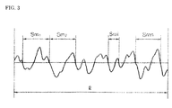
- the average concave-concave/convex-convex interval was found as follows. From the roughness curve, a part corresponding to the reference length (I) in the direction of the average line was extracted. Regarding the extracted part, a length of the average line corresponding to one peak and a length of the average line corresponding to a trough adjacent to the peak were added together (hereinafter, this sum will be referred to as the "concave-concave/convex-convex interval"). The arithmetic average value of such intervals measured on many concaves and convexes was obtained. According to the standards, the arithmetic average value is represented on the unit of millimeter (mm).
- Sm the unit of micrometer ( ⁇ m) because the target range was narrow. Namely, Sm can be found by the following expression.
- the method for calculating Sm can be shown as in FIG. 3 .
- the average inter-local peak interval was found as follows. From the roughness curve, a part corresponding to the reference length in the direction of the average line was extracted. Regarding the extracted part, a length of the average line corresponding to the interval between two adjacent local peaks (hereinafter, will be referred to as the "inter-local peak interval") was obtained. The arithmetic average value of such intervals measured on many local peaks was obtained.
- a pellet of a polycarbonate resin (Iupilon E-2000 produced by Mitsubishi Engineering-Plastics Corporation) was dried at 120°C for 3 hours by a hot air drier.
- the resultant pellet was melt-extruded at 270°C by a 90 mm monoaxial extruder and a T-die.
- the extruded melted film was nipped by a silicone rubber first cooling roll having a diameter of 220 mm and a metallic second cooling roll having a diameter of 450 mm and having an embossed surface with an arithmetic average roughness of 2.4 ⁇ m. Then, an emboss pattern was formed on a surface of the film.
- the film was cooled, and then passed through a metallic third cooling roll having a mirror surface.
- a film having a thickness of 130 ⁇ m with one surface being embossed was produced while being taken up by a take-up roll.
- the temperature of the first cooling roll was set to 50°C
- the temperature of the second cooling roll was set to 130°C
- the temperature of the third cooling roll was set to 130°C.
- the rate of the cooling rolls was set to 9.9 m/min.
- Table 1 By attaching the polycarbonate resin film according to this example, the measured luminance was significantly improved.
- a pellet of a polycarbonate resin (Iupilon E-2000 produced by Mitsubishi Engineering-Plastics Corporation) was dried at 120°C for 3 hours by a hot air drier.
- the resultant pellet was melt-extruded at 270°C by a 90 mm monoaxial extruder and a T-die.
- the extruded melted film was nipped by a silicone rubber first cooling roll having a diameter of 220 mm and a metallic second cooling roll having a diameter of 450 mm and having an embossed surface with an arithmetic average roughness of 2.4 ⁇ m. Then, an emboss pattern was formed on a surface of the film.
- the film was cooled, and then passed through a metallic third cooling roll having a mirror surface.
- a film having a thickness of 75 ⁇ m with one surface being embossed was produced while being taken up by a take-up roll.
- the temperature of the first cooling roll was set to 60°C
- the temperature of the second cooling roll was set to 135°C
- the temperature of the third cooling roll was set to 135°C.
- the rate of the cooling rolls was set to 17.0 m/min.
- the evaluation results on the characteristics of the obtained film are shown in Table 1.
- a pellet of a polycarbonate resin (Iupilon E-2000 produced by Mitsubishi Engineering-Plastics Corporation) was dried at 120°C for 3 hours by a hot air drier.
- the resultant pellet was melt-extruded at 270°C by a 90 mm monoaxial extruder and a T-die.
- the extruded melted film was nipped by a silicone rubber first cooling roll having a diameter of 220 mm and a metallic second cooling roll having a diameter of 450 mm and having an embossed surface with an arithmetic average roughness of 0.8 ⁇ m. Then, an emboss pattern was formed on a surface of the film.
- the film was cooled, and then passed through a metallic third cooling roll having a mirror surface.
- a film having a thickness of 130 ⁇ m with one surface being embossed was produced while being taken up by a take-up roll.
- the temperature of the first cooling roll was set to 50°C
- the temperature of the second cooling roll was set to 130°C
- the temperature of the third cooling roll was set to 130°C.
- the rate of the cooling rolls was set to 9.9 m/min.
- the evaluation results on the characteristics of the obtained film are shown in Table 1. Even by attaching the polycarbonate resin film according to this example, the measured luminance was not significantly improved.
Landscapes
- Physics & Mathematics (AREA)
- Chemical & Material Sciences (AREA)
- Engineering & Computer Science (AREA)
- Manufacturing & Machinery (AREA)
- Optics & Photonics (AREA)
- General Physics & Mathematics (AREA)
- Chemical Kinetics & Catalysis (AREA)
- Organic Chemistry (AREA)
- Medicinal Chemistry (AREA)
- Health & Medical Sciences (AREA)
- Materials Engineering (AREA)
- Polymers & Plastics (AREA)
- Nonlinear Science (AREA)
- Mechanical Engineering (AREA)
- Crystallography & Structural Chemistry (AREA)
- Mathematical Physics (AREA)
- Optical Elements Other Than Lenses (AREA)
- Extrusion Moulding Of Plastics Or The Like (AREA)
- Manufacture Of Macromolecular Shaped Articles (AREA)
- Shaping Of Tube Ends By Bending Or Straightening (AREA)
- Liquid Crystal (AREA)
Abstract
Description
- The present invention relates to a polymer film usable for displays such as liquid crystal displays (LCDs) and in the field of optical devices. In more detail, the present invention relates to a film suitable to improve the luminance and the contrast of liquid crystal displays.
- Conventionally, in display devices for, for example, displaying numerical figures or letters or performing planar light emission using point light sources such as light emitting diodes or linear light sources such as fluorescent lamps or cathode ray tubes, optical diffusion films are used which diffuse the transmitted light from the point or linear light sources to make the light appear to be from planar light sources.
- In the field of flat panel displays (FPDs), it is desired to alleviate the nonuniformity in the luminance and to improve the luminance in order to realize higher display performances.
- A general backlight unit of a liquid crystal display includes a waveguide plate having optical diffusion dots printed on a rear surface thereof, a light source (cathode ray tube, etc.) located on one side or both of two sides of the waveguide plate, an optical diffusion sheet provided on the waveguide plate, a lens film (prism sheet) provided optionally on an upper surface, or both on upper and lower surfaces, of the optical diffusion sheet, and the like.
- The optical diffusion sheet incorporated into such a backlight unit uniformly diffuses light from the waveguide plate to prevent the dots from being visible on the display screen and uniformly releases the diffused light toward the liquid crystal panel while suppressing the optical loss.
- Several types of such an optical diffusion sheet have been conventionally proposed. In order to achieve the above-described object, for example, Japanese Laid-Open Patent Publication No.
11-337711 - Japanese Laid-Open Patent Publication No.
2003-107214 - However, the optical diffusion sheets as disclosed in Japanese Laid-Open Patent Publications Nos.
11-337711 2003-107214 - In order to solve these problems, Japanese Laid-Open Patent Publication No.
2002-357706 - Japanese Laid-Open Patent Publication No.
2002-202508 - The above-identified publication also describes that in the case where the diffusing section is formed by embossing, the light beam can be diffused more conspicuously where the surface roughness Rz is 5 µm or greater and 50 µm or less. However, it is difficult to provide, at the same time, an optical diffusion function, an improved luminance, a transmittance and the like which are of a sufficient level by merely limiting Rz.
- Japanese Laid-Open Patent Publication No.
2003-329812 - With this proposal, the optical diffusion function provided by the embossed surface as defined above is insufficient and a separate optical diffusion layer is necessary. This makes the production method troublesome and involves the problems of optical loss and cost increase.
- Japanese Laid-Open Patent Publication No.
2004-4417 2003-329812 - As described above, with the conventionally proposed optical diffusion films, which are formed of binder resins and have resin particles dispersed therein, the display quality is low and the optical loss is not negligible. So far, no film having an embossed concaved and convexed surface for expressing an optical diffusion function provides, at the same time, an optical diffusion function, an improved luminance, a transmittance and the like which are of a sufficient level.
- As a result of active studies performed in order to solve the above-described problems, the present inventor found that a polymer film having an Ra (arithmetic average roughness) of 0.5 µm to 2.5 µm, an Ry (maximum height) of 3 µm to 1 µm, an Rz (ten-point average height) of 3 µm to 8 µm and a light transmittance of 85% or higher provides, at the same time, an optical diffusion function, an improved luminance, a transmittance and the like, which are of a sufficient level not realized conventionally, and achieved the present invention. The present inventor also found that where Sm (average concave-concave/convex-convex interval) is 90 µm to 160 mm and the average inter-local peak interval (S) is 5 µm to 15 µm, an especially preferable performance is provided. The polymer film according to the present invention can be produced by melt extrusion.
-
-
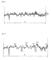
FIG. 1 shows how to calculate the arithmetic average roughness (Ra). -
FIG. 2 shows how to calculate the ten-point average roughness (Rz). -
FIG. 3 shows how to calculate the average concave-concave/convex-convex interval (Sm). - Hereinafter, the present invention will be described in more detail.
- The polymer film according to the present invention has an arithmetic average roughness Ra of 0.5 µm to 2.5 µm. A method for measuring the arithmetic average roughness Ra according to the present invention is described in the Examples section below. The arithmetic average roughness Ra according to the present invention is preferably 1.0 µm to 2.0 µm.
- The polymer film according to the present invention has a maximum height Ry of 3 µm to 11 µm. A method for measuring the maximum height Ry according to the present invention is described in the Examples section below. The maximum height Ry according to the present invention is preferably 5 µm to 10 µm.
- The polymer film according to the present invention has a ten-point average height Rz of 3 µm to 8 µm. A method for measuring the ten-point average height Rz according to the present invention is described in the Examples section below. The ten-point average height Rz according to the present invention is preferably 4 µm to 7 µm.
- The polymer film according to the present invention has a light transmittance of 85% or higher. A method for measuring the light transmittance according to the present invention is described in the Examples section below. The light transmittance of 85% or higher is preferable because the optical loss is suppressed to be low and the decrease in the luminance is reduced.
- The polymer film according to the present invention preferably has an average concave-concave/convex-convex interval Sm of 90 µm to 160 µm. A method for measuring the average concave-concave/convex-convex interval Sm according to the present invention is described in the Examples section below. More preferably, the average concave-concave/convex-convex interval Sm is 100 µm to 150 µm.
- The polymer film according to the present invention preferably has an average inter-local peak interval S of 5 µm to 15 µm. A method for measuring the average inter-local peak interval according to the present invention is described in the Examples section below. More preferably, the average inter-local peak interval S is 7 µm to 12 µm.
- The polymer film according to the present invention preferably has a haze of 50% or higher. A method for measuring the haze according to the present invention is described in the Examples section below. The haze of 50% or higher is preferable because the diffusion effect is significant.
- It is not preferable that the surface roughness is too small because although the light transmittance is maintained, the optical diffusion function and the luminance improving function are small. It is not preferable either that the surface roughness is too large because small nonuniformity in the luminance is left without disappearing. The surface roughness cannot be sufficiently defined by only Rz and is preferably defined also by Ra and Ry. It is not preferable that the concave-concave/convex-convex interval is too large because the number of the concaves and convexes per unit area size is small and therefore the diffusion effect and the luminance improving effect are small.
- In order to achieve the surface roughness according to the present invention, the surface roughness of an embossed metallic cooling roll is most important. The surface roughness is defined by the rolling rate and the temperature.
- As a phase film, any film having a high light transmittance is usable with no specific limitation. A film having a light transmittance of 85% or higher and little alignment nonuniformity is preferably usable. Materials usable for such a film include, for example, polyesters such as polycarbonate, polyarylate, polysulfone, PET, polyethylene naphthalate and the like; polyolefins such as polyether sulfone, polyvinyl alcohol, polyethylene, polypropylene and the like; cellulose-based polymers; polystyrene; polymethyl methacrylate; polyvinyl chloride; polyvinylidene chloride; polyamide; norbornene-based polylmers; and the like. Among these, polycarbonate is especially preferably usable.
- Polycarbonate can be produced by a known method of using a bisphenol and a carbonic acid ester forming compound. Polycarbonate can be produced by, for example, direct reaction of a bisphenol and a phosgene (phosgene method), transesterification reaction of a bisphenol and a bisarylcarbonate (transesterification method), or the like.
- The bisphenols include, for example, 2,2-bis(4-hydroxyphenyl)propane (generally called "bisphenol A") , bis(4-hydroxyphenyl)methane; 1,1-bis(4-hydroxyphenyl)ethane; 2,2-bis(4-hydroxyphenyl)butane; 2,2-bis(4-hydroxyphenyl)octane; 2,2-bis(4-hydroxyphenyl)phenylmethane; bis(hydroxyaryl)alkanes such as 2,2-bis(4-hydroxy-1-methylphenyl)propane, 2,2-bis(3-methyl-4-hydroxyphenyl)propane, 2,2-bis(3,5-dimethyl-4-hydroxyphenyl)propane, bis(4-hydroxyphenyl)naphtylmethane, 1,1-bis(4-hydroxy-t-butylphenyl)propane, 2,2-bis(4-hydroxy-3-bromophenyl)propane, 2,2-bis(4-hydroxy-3,5-tetramethylphenyl)propane, 2,2-bis(4-hydroxy-3-chlorophenyl)propane, 2,2-bis(4-hydroxy-3,5-tetrachlorophenyl)propane, 2,2-bis(4-hydroxy-3,5-tetrabromophenyl)propane and the like; bis(hydroxyaryl)cycloalkanes such as 1,1-bis(4-hydroxyphenyl)cyclopentane, 1,1-bis(4-hydroxyphenyl)cyclohexane (generally called "bisphenol Z"), 1,1-bis(4-hydroxyphenyl)-3,5,5-trimethylcyclohexane, and the like; bis(hydroxyaryl)sulfides such as bis(4-hydroxyphenyl)sulfide, and the like; and bis(hydroxyaryl)sulfones such as bis(4-hydroxyphenyl)sulfone, and the like.
- 2,2-bis(4-hydroxyphenyl)propane (generally called "bisphenol A") is especially preferable.
- The carbonic acid ester forming compounds include, for example, bisarylcarbonates such as phosgene, triphosgene, diphenyl carbonate, di-p-tolyl carbonate, phenyl-p-tolyl carbonate, di-p-chlorophenyl carbonate, dinaphthyl carbonate, and the like. These compounds may be used in a combination of two or more.
- Within the range of the object of the present invention, any of the following is usable together with any of the bisphenols mentioned above: tricyclo[5.2.1.02,6]decanedimethanol, cyclohexane-1,4-dimethanol, decalin-2,6-dimethanol, norbornanedimethanol, pentacyclopentadecanedimethanol, cyclopentane-1,3-dimethanol, 1,4-butanediol, 1,6-hexanediol, spiroglycol, isosorbide, isomannide, and the like.
- The polymer film according to the present invention preferably has a function corresponding to a haze of 50% or higher by having a concaved and convexed pattern on at least one surface. The surface pattern is preferably an embossed pattern, a V-shaped groove pattern, a ridge pattern or the like which highly diffuses light. An embossed pattern is especially preferable. A film, which has a concaved and convexed pattern on a surface thereof, has the light transmittance and the haze increased and thus provides a high optical diffusion performance.
- The resin film according to the present invention can be produced using a normal melt extrusion molding apparatus. A melted resin film melted by an extruder and discharged from a T-die is nipped by a first cooling roll having a rubber elasticity and a metallic second cooling roll having an embossed surface to form a concaved and convexed pattern on a surface of the film. The film is taken up by a metallic third cooling roll and a take-up roll provided downstream with respect to the first and second cooling rolls.
- Hereinafter, the present invention will be described by way of examples. The present invention is not limited to the following examples in any way. The characteristics were evaluated as follows.
- (1) Total light transmittance and haze
These were measured by haze meter HM-150 produced by Murakami Color Research Laboratory Co., Ltd. - (2) Front luminance
The front luminance was measured by a luminometer (LS-110 produced by Minolta) set at a position 30 cm away from the light emitting surface of a backlight unit having a size of 7 cm x 9 cm.
A diffusion film cut into a size of 6.5 cm x 8.5 cm was attached on the light emitting surface of the backlight in such a direction that the concaved and convexed surface was directed toward the light source and fixed with a tape, and the front luminance was measured by the luminometer. - (3) Measurement of the surface roughness of the film
- As the measuring device, an ultra-depth shape measuring microscope VK-8500 produced by Keyence Corporation was used. The settings for the measurement were as follows: objective lens: x50; shutter: automatic; gain: automatic. The pitch was 0.1 µm.
- The arithmetic average roughness was found as follows. From the roughness curve, a part corresponding to the reference length (1) in the direction of the average line was extracted. The X axis was set to the direction of the average line of the extracted part, and the Y axis was set to the direction perpendicular to the X axis. The roughness curve was represented by y = f(x). The value obtained by the following expression in this setting was represented by micrometer (µm). The method for calculating Ra can be shown as in
FIG. 1 .
- The maximum height was found as follows. From the roughness curve, a part corresponding to the reference length in the direction of the average line was extracted. The interval between the peak line and the trough line of the extracted part was measured in the direction perpendicular to the roughness curve, and the obtained value was represented by micrometer (µm).
- The ten-point average roughness was found as follows. From the roughness curve, a part corresponding to the reference length (1) in the direction of the average line was extracted. The elevations (Yp) of the highest peak through the fifth highest peak were measured in the direction perpendicular to the average line of the extracted part. The elevations (Yv) of the deepest trough through the fifth deepest trough were measured in the direction perpendicular to the average line of the extracted part. The average of the absolute values of the elevations (Yp) and the average of the absolute values of the elevations (Yv) were added together, and the obtained sum was represented by micrometer (µm). Namely, Rz can be obtained by the following expression. The method for calculating Rz can be shown as in
FIG. 2 .
Ypl+Yp2+Yp3+Yp4+Yp5: elevation of the highest peak through the fifth highest peak of the extracted part of the reference length (I)
Yvl+Yv2+Yv3+Yv4+Yv5: elevation of the deepest trough through the fifth deepest trough of the extracted part of the reference length (1) - The average concave-concave/convex-convex interval was found as follows. From the roughness curve, a part corresponding to the reference length (I) in the direction of the average line was extracted. Regarding the extracted part, a length of the average line corresponding to one peak and a length of the average line corresponding to a trough adjacent to the peak were added together (hereinafter, this sum will be referred to as the "concave-concave/convex-convex interval"). The arithmetic average value of such intervals measured on many concaves and convexes was obtained. According to the standards, the arithmetic average value is represented on the unit of millimeter (mm). However, with this device, the unit of micrometer (µm) was used because the target range was narrow. Namely, Sm can be found by the following expression. The method for calculating Sm can be shown as in
FIG. 3 .
- The average inter-local peak interval was found as follows. From the roughness curve, a part corresponding to the reference length in the direction of the average line was extracted. Regarding the extracted part, a length of the average line corresponding to the interval between two adjacent local peaks (hereinafter, will be referred to as the "inter-local peak interval") was obtained. The arithmetic average value of such intervals measured on many local peaks was obtained.
- A pellet of a polycarbonate resin (Iupilon E-2000 produced by Mitsubishi Engineering-Plastics Corporation) was dried at 120°C for 3 hours by a hot air drier. The resultant pellet was melt-extruded at 270°C by a 90 mm monoaxial extruder and a T-die. The extruded melted film was nipped by a silicone rubber first cooling roll having a diameter of 220 mm and a metallic second cooling roll having a diameter of 450 mm and having an embossed surface with an arithmetic average roughness of 2.4 µm. Then, an emboss pattern was formed on a surface of the film. The film was cooled, and then passed through a metallic third cooling roll having a mirror surface. Thus, a film having a thickness of 130 µm with one surface being embossed was produced while being taken up by a take-up roll. In this procedure, the temperature of the first cooling roll was set to 50°C, the temperature of the second cooling roll was set to 130°C, and the temperature of the third cooling roll was set to 130°C. The rate of the cooling rolls was set to 9.9 m/min. The evaluation results on the characteristics of the obtained film are shown in Table 1. By attaching the polycarbonate resin film according to this example, the measured luminance was significantly improved.
- A pellet of a polycarbonate resin (Iupilon E-2000 produced by Mitsubishi Engineering-Plastics Corporation) was dried at 120°C for 3 hours by a hot air drier. The resultant pellet was melt-extruded at 270°C by a 90 mm monoaxial extruder and a T-die. The extruded melted film was nipped by a silicone rubber first cooling roll having a diameter of 220 mm and a metallic second cooling roll having a diameter of 450 mm and having an embossed surface with an arithmetic average roughness of 2.4 µm. Then, an emboss pattern was formed on a surface of the film. The film was cooled, and then passed through a metallic third cooling roll having a mirror surface. Thus, a film having a thickness of 75 µm with one surface being embossed was produced while being taken up by a take-up roll. In this procedure, the temperature of the first cooling roll was set to 60°C, the temperature of the second cooling roll was set to 135°C, and the temperature of the third cooling roll was set to 135°C. The rate of the cooling rolls was set to 17.0 m/min. The evaluation results on the characteristics of the obtained film are shown in Table 1. By attaching the polycarbonate resin film according to this example, the measured luminance was significantly improved.
- A pellet of a polycarbonate resin (Iupilon E-2000 produced by Mitsubishi Engineering-Plastics Corporation) was dried at 120°C for 3 hours by a hot air drier. The resultant pellet was melt-extruded at 270°C by a 90 mm monoaxial extruder and a T-die. The extruded melted film was nipped by a silicone rubber first cooling roll having a diameter of 220 mm and a metallic second cooling roll having a diameter of 450 mm and having an embossed surface with an arithmetic average roughness of 0.8 µm. Then, an emboss pattern was formed on a surface of the film. The film was cooled, and then passed through a metallic third cooling roll having a mirror surface. Thus, a film having a thickness of 130 µm with one surface being embossed was produced while being taken up by a take-up roll. In this procedure, the temperature of the first cooling roll was set to 50°C, the temperature of the second cooling roll was set to 130°C, and the temperature of the third cooling roll was set to 130°C. The rate of the cooling rolls was set to 9.9 m/min. The evaluation results on the characteristics of the obtained film are shown in Table 1. Even by attaching the polycarbonate resin film according to this example, the measured luminance was not significantly improved.
- The measurement was performed in substantially the same manner as in Examples 1 and 2 using polycarbonate film ECG100-80 produced by Tsutsunaka Plastic Industry Co., Ltd. The evaluation results on the characteristics of the obtained film are shown in Table 1.
- The measurement was performed in substantially the same manner as in Examples 1 and 2 using polycarbonate film ECG100S produced by Tsutsunaka Plastic Industry Co., Ltd. The evaluation results on the characteristics of the obtained film are shown in Table 1.
Table 1 Ex. 1 Ex. 2 Comparative ex. 1 Comparative ex. 2 Comparative ex. 3 Film thickness (µm) 130 75 130 130 300 Haze (%) 79 71 14 78 69 Total light transmittance (%) 87 88 89 89 88 Ra(µm) 1.6 1.5 0.4 2.9 3.0 Ry(µm) 7.9 8.1 1.9 12.4 13.8 Rz(µm) 4.9 5.0 1.1 9.9 9.1 Sm(µm) 112 150 81 157 120 S(µm) 10 9 7.4 5 13 Front luminance ratio 1.10 1.08 1.04 1.06 1.05
Claims (5)
- A polymer film having an arithmetic average roughness Ra of 0.5 µm to 2.5 µm, a maximum height Ry of 3 µm to 11 µm, a ten-point average height Rz of 3 µm to 8 µm, and a light transmittance of 85% or higher.
- The polymer film according to claim 1, which has an average concave-concave/convex-convex interval Sm of 90 µm to 160 µm, and an average inter-local peak interval S of 5 µm to 15 µm.
- The polymer film according to claim 1 or 2, which has a haze of 50% or higher.
- The polymer film according to any one of claims 1 through 3, which is produced by melt extrusion.
- The polymer film according to any one of claims 1 through 4, which contains a polycarbonate resin.
Applications Claiming Priority (2)
| Application Number | Priority Date | Filing Date | Title |
|---|---|---|---|
| JP2006354246 | 2006-12-28 | ||
| PCT/JP2007/075337 WO2008081953A1 (en) | 2006-12-28 | 2007-12-21 | Polymer film |
Publications (3)
| Publication Number | Publication Date |
|---|---|
| EP2098357A1 true EP2098357A1 (en) | 2009-09-09 |
| EP2098357A4 EP2098357A4 (en) | 2010-03-10 |
| EP2098357B1 EP2098357B1 (en) | 2012-06-06 |
Family
ID=39588631
Family Applications (1)
| Application Number | Title | Priority Date | Filing Date |
|---|---|---|---|
| EP07851131A Active EP2098357B1 (en) | 2006-12-28 | 2007-12-21 | Polymer film |
Country Status (7)
| Country | Link |
|---|---|
| US (1) | US8790766B2 (en) |
| EP (1) | EP2098357B1 (en) |
| JP (1) | JP5261193B2 (en) |
| KR (1) | KR101441714B1 (en) |
| CN (1) | CN101622120B (en) |
| TW (1) | TWI417610B (en) |
| WO (1) | WO2008081953A1 (en) |
Cited By (1)
| Publication number | Priority date | Publication date | Assignee | Title |
|---|---|---|---|---|
| EP3306358A4 (en) * | 2015-06-04 | 2018-12-26 | Mitsubishi Gas Chemical Company, Inc. | Polymer film, and light diffusion film comprising same for display |
Families Citing this family (13)
| Publication number | Priority date | Publication date | Assignee | Title |
|---|---|---|---|---|
| KR100963674B1 (en) * | 2007-12-05 | 2010-06-15 | 제일모직주식회사 | Light diffusing film having uniform surface roughness and low retardation value and manufacturing method thereof |
| KR101570257B1 (en) | 2008-05-19 | 2015-11-18 | 덴카 주식회사 | Film and method of film processing |
| JP2010286827A (en) * | 2009-05-14 | 2010-12-24 | Jiroo Corporate Plan:Kk | Polarizer protective film, polarizing plate and liquid crystal display element |
| JP6266856B2 (en) * | 2011-04-12 | 2018-01-24 | 恵和株式会社 | Polarized sunglasses |
| CN103890618B (en) | 2011-10-24 | 2016-11-16 | 三菱瓦斯化学株式会社 | light scattering film |
| JP5719864B2 (en) * | 2013-04-09 | 2015-05-20 | 長岡産業株式会社 | Transparent conductive film |
| JP6542602B2 (en) * | 2015-07-23 | 2019-07-10 | 帝人株式会社 | the film |
| JP6647761B2 (en) * | 2015-12-07 | 2020-02-14 | 恵和株式会社 | Top light diffusion sheet and backlight unit |
| US10222518B2 (en) | 2015-12-07 | 2019-03-05 | Keiwa Inc. | Light diffusion sheet for overlaying, and backlight unit |
| CN107089003A (en) * | 2017-05-31 | 2017-08-25 | 山西宇皓新型光学材料有限公司 | Light-conducting board mold, light guide plate and preparation method thereof |
| CN111031786B (en) * | 2017-09-26 | 2022-09-20 | Agc株式会社 | Fluororesin film for agriculture and greenhouse for agriculture |
| WO2019078290A1 (en) * | 2017-10-19 | 2019-04-25 | デンカ株式会社 | Single-layer film and heat-resistant adhesive tape using same |
| JP7286269B2 (en) * | 2018-03-23 | 2023-06-05 | 恵和株式会社 | backlight unit |
Family Cites Families (23)
| Publication number | Priority date | Publication date | Assignee | Title |
|---|---|---|---|---|
| CA2024770A1 (en) | 1989-09-14 | 1991-03-15 | Shigeru Nedzu | Transparent polybutylene terephthalate resin film and process for producing the same |
| JP4148582B2 (en) | 1998-12-21 | 2008-09-10 | 東レ・ダウコーニング株式会社 | Gas permeable film |
| JPH11337711A (en) | 1999-04-21 | 1999-12-10 | Tsujiden:Kk | High light diffusion film |
| JP2000352607A (en) * | 1999-06-11 | 2000-12-19 | Dainippon Printing Co Ltd | Light diffusion film, manufacturing method thereof, surface light source, and display device |
| US20020018883A1 (en) | 2000-07-05 | 2002-02-14 | Iwao Okazaki | Thermoplastic resin film and production process thereof, and optical film |
| JP4067814B2 (en) | 2000-11-22 | 2008-03-26 | タキロン株式会社 | Light diffusion sheet |
| JP2002241514A (en) * | 2001-02-19 | 2002-08-28 | Daiya Plastic Kk | Ethylene resin film excellent in anti-blocking property and method for producing the same |
| JP2002357706A (en) | 2001-06-01 | 2002-12-13 | Keiwa Inc | Optical sheet and backlight unit using the same |
| JP3940281B2 (en) | 2001-09-28 | 2007-07-04 | 株式会社きもと | Light diffusing sheet |
| JP4995385B2 (en) | 2001-09-28 | 2012-08-08 | 恵和株式会社 | Light diffusion sheet and backlight unit using the same |
| WO2003044572A1 (en) * | 2001-11-22 | 2003-05-30 | Takiron Co., Ltd. | Light diffusive sheet |
| JP2002202508A (en) | 2001-12-17 | 2002-07-19 | Keiwa Inc | Device to illuminate LCD screen |
| KR100951285B1 (en) | 2002-03-06 | 2010-04-02 | 키모토 컴파니 리미티드 | Light diffusion sheet and surface light source element |
| JP2004004417A (en) | 2002-04-18 | 2004-01-08 | Nitto Denko Corp | Light diffusion sheet, optical element and image display device |
| JP2004155101A (en) | 2002-11-07 | 2004-06-03 | Keiwa Inc | Optical sheet and method for manufacturing the optical sheet |
| US6913714B2 (en) | 2002-11-21 | 2005-07-05 | Bayer Materialscience Llc | Method of producing thermoplastic polycarbonate films having low optical retardation values |
| US7196845B2 (en) * | 2003-02-18 | 2007-03-27 | Mitsubishi Gas Chemical Company, Inc. | Fresnel lens sheet and rear projection screen |
| TW200600825A (en) * | 2004-03-16 | 2006-01-01 | Tomoegawa Paper Co Ltd | Anisotropic light diffusion medium and production method therefor |
| JP2006091836A (en) | 2004-08-26 | 2006-04-06 | Nitto Denko Corp | Retardation film and method for producing the same, and optical film, liquid crystal panel and liquid crystal display device using the retardation film |
| TWI383003B (en) * | 2005-02-02 | 2013-01-21 | 三菱瓦斯化學股份有限公司 | Polyester film, its preparation method, and use thereof |
| WO2007044063A2 (en) | 2005-04-12 | 2007-04-19 | Arkema France | Transparent bullet-resistant acrylic sheet |
| DE102005050072A1 (en) | 2005-10-19 | 2007-04-26 | Bayer Materialscience Ag | Diffusing films and their use in flat screens |
| DE102006051306A1 (en) | 2006-10-31 | 2008-05-08 | Bayer Materialscience Ag | Substrate materials for extrusion foils with low surface defects |
-
2007
- 2007-12-21 KR KR1020097015578A patent/KR101441714B1/en active Active
- 2007-12-21 CN CN200780046713XA patent/CN101622120B/en active Active
- 2007-12-21 JP JP2008552196A patent/JP5261193B2/en active Active
- 2007-12-21 EP EP07851131A patent/EP2098357B1/en active Active
- 2007-12-21 WO PCT/JP2007/075337 patent/WO2008081953A1/en not_active Ceased
- 2007-12-21 US US12/520,558 patent/US8790766B2/en active Active
- 2007-12-26 TW TW096150205A patent/TWI417610B/en active
Cited By (1)
| Publication number | Priority date | Publication date | Assignee | Title |
|---|---|---|---|---|
| EP3306358A4 (en) * | 2015-06-04 | 2018-12-26 | Mitsubishi Gas Chemical Company, Inc. | Polymer film, and light diffusion film comprising same for display |
Also Published As
| Publication number | Publication date |
|---|---|
| US20100136287A1 (en) | 2010-06-03 |
| CN101622120A (en) | 2010-01-06 |
| US8790766B2 (en) | 2014-07-29 |
| JPWO2008081953A1 (en) | 2010-04-30 |
| TWI417610B (en) | 2013-12-01 |
| KR101441714B1 (en) | 2014-09-17 |
| WO2008081953A1 (en) | 2008-07-10 |
| TW200844573A (en) | 2008-11-16 |
| EP2098357B1 (en) | 2012-06-06 |
| JP5261193B2 (en) | 2013-08-14 |
| CN101622120B (en) | 2013-06-26 |
| KR20090108606A (en) | 2009-10-15 |
| EP2098357A4 (en) | 2010-03-10 |
Similar Documents
| Publication | Publication Date | Title |
|---|---|---|
| EP2098357B1 (en) | Polymer film | |
| US8325418B2 (en) | Optical film, its manufacturing method, anti-glare polarizer using the same, and display apparatus | |
| JP4412425B2 (en) | Prism sheet, backlight unit using the same, and liquid crystal display device | |
| KR100977321B1 (en) | Light transmissive resin plate | |
| US20080285255A1 (en) | Low birefringent light redirecting film | |
| KR101629469B1 (en) | Light guide film, ultra-thin liquid crystal backlight unit and portable computer | |
| JP2009058862A (en) | Anti-glare film | |
| JP2009169409A (en) | Anti-glare film, anti-glare polarizing plate and image display device | |
| KR101428127B1 (en) | Backlight device | |
| JP2008145499A (en) | Anti-glare light diffusing member | |
| TW201303380A (en) | Light diffusion film, method for producing the same, coating liquid used therefor, and polarizing plate and liquid crystal display device using the same | |
| WO2007146663A1 (en) | Diffuser films and methods for making and using the same | |
| JP2009512747A (en) | Light scattering film and its use in flat screen | |
| KR20230002866A (en) | Optical sheets, backlight units, liquid crystal displays and information devices | |
| KR100940363B1 (en) | Prism Shape Control Method and Controlled Optical Film | |
| JP7279062B2 (en) | Light guide laminate using anisotropic optical film, and planar illumination device for display using the same | |
| KR101068635B1 (en) | High Brightness Diffusion Film with Improved Engraving Rate and Its Manufacturing Method | |
| TWI416225B (en) | Phase difference film | |
| JP2011214836A (en) | Defect inspection method of thermoplastic resin sheet | |
| KR20080065341A (en) | Light Diffusion Plate for Backlight Unit | |
| KR101292653B1 (en) | Optical film improved brightness and Preparing thereof | |
| JP2015004859A (en) | Anisotropic light diffusion film | |
| KR20100104615A (en) | Diffussion film with the improved brightness and preparing thereof |
Legal Events
| Date | Code | Title | Description |
|---|---|---|---|
| PUAI | Public reference made under article 153(3) epc to a published international application that has entered the european phase |
Free format text: ORIGINAL CODE: 0009012 |
|
| 17P | Request for examination filed |
Effective date: 20090706 |
|
| AK | Designated contracting states |
Kind code of ref document: A1 Designated state(s): AT BE BG CH CY CZ DE DK EE ES FI FR GB GR HU IE IS IT LI LT LU LV MC MT NL PL PT RO SE SI SK TR |
|
| A4 | Supplementary search report drawn up and despatched |
Effective date: 20100205 |
|
| DAX | Request for extension of the european patent (deleted) | ||
| 17Q | First examination report despatched |
Effective date: 20100324 |
|
| GRAP | Despatch of communication of intention to grant a patent |
Free format text: ORIGINAL CODE: EPIDOSNIGR1 |
|
| GRAC | Information related to communication of intention to grant a patent modified |
Free format text: ORIGINAL CODE: EPIDOSCIGR1 |
|
| GRAS | Grant fee paid |
Free format text: ORIGINAL CODE: EPIDOSNIGR3 |
|
| GRAA | (expected) grant |
Free format text: ORIGINAL CODE: 0009210 |
|
| AK | Designated contracting states |
Kind code of ref document: B1 Designated state(s): AT BE BG CH CY CZ DE DK EE ES FI FR GB GR HU IE IS IT LI LT LU LV MC MT NL PL PT RO SE SI SK TR |
|
| REG | Reference to a national code |
Ref country code: GB Ref legal event code: FG4D |
|
| REG | Reference to a national code |
Ref country code: AT Ref legal event code: REF Ref document number: 560798 Country of ref document: AT Kind code of ref document: T Effective date: 20120615 Ref country code: CH Ref legal event code: EP |
|
| REG | Reference to a national code |
Ref country code: IE Ref legal event code: FG4D |
|
| REG | Reference to a national code |
Ref country code: DE Ref legal event code: R096 Ref document number: 602007023228 Country of ref document: DE Effective date: 20120809 |
|
| REG | Reference to a national code |
Ref country code: NL Ref legal event code: VDEP Effective date: 20120606 |
|
| PG25 | Lapsed in a contracting state [announced via postgrant information from national office to epo] |
Ref country code: SE Free format text: LAPSE BECAUSE OF FAILURE TO SUBMIT A TRANSLATION OF THE DESCRIPTION OR TO PAY THE FEE WITHIN THE PRESCRIBED TIME-LIMIT Effective date: 20120606 Ref country code: LT Free format text: LAPSE BECAUSE OF FAILURE TO SUBMIT A TRANSLATION OF THE DESCRIPTION OR TO PAY THE FEE WITHIN THE PRESCRIBED TIME-LIMIT Effective date: 20120606 Ref country code: CY Free format text: LAPSE BECAUSE OF FAILURE TO SUBMIT A TRANSLATION OF THE DESCRIPTION OR TO PAY THE FEE WITHIN THE PRESCRIBED TIME-LIMIT Effective date: 20120606 Ref country code: FI Free format text: LAPSE BECAUSE OF FAILURE TO SUBMIT A TRANSLATION OF THE DESCRIPTION OR TO PAY THE FEE WITHIN THE PRESCRIBED TIME-LIMIT Effective date: 20120606 |
|
| REG | Reference to a national code |
Ref country code: AT Ref legal event code: MK05 Ref document number: 560798 Country of ref document: AT Kind code of ref document: T Effective date: 20120606 |
|
| REG | Reference to a national code |
Ref country code: LT Ref legal event code: MG4D Effective date: 20120606 |
|
| PG25 | Lapsed in a contracting state [announced via postgrant information from national office to epo] |
Ref country code: SI Free format text: LAPSE BECAUSE OF FAILURE TO SUBMIT A TRANSLATION OF THE DESCRIPTION OR TO PAY THE FEE WITHIN THE PRESCRIBED TIME-LIMIT Effective date: 20120606 Ref country code: GR Free format text: LAPSE BECAUSE OF FAILURE TO SUBMIT A TRANSLATION OF THE DESCRIPTION OR TO PAY THE FEE WITHIN THE PRESCRIBED TIME-LIMIT Effective date: 20120907 Ref country code: LV Free format text: LAPSE BECAUSE OF FAILURE TO SUBMIT A TRANSLATION OF THE DESCRIPTION OR TO PAY THE FEE WITHIN THE PRESCRIBED TIME-LIMIT Effective date: 20120606 |
|
| PG25 | Lapsed in a contracting state [announced via postgrant information from national office to epo] |
Ref country code: EE Free format text: LAPSE BECAUSE OF FAILURE TO SUBMIT A TRANSLATION OF THE DESCRIPTION OR TO PAY THE FEE WITHIN THE PRESCRIBED TIME-LIMIT Effective date: 20120606 Ref country code: NL Free format text: LAPSE BECAUSE OF FAILURE TO SUBMIT A TRANSLATION OF THE DESCRIPTION OR TO PAY THE FEE WITHIN THE PRESCRIBED TIME-LIMIT Effective date: 20120606 Ref country code: RO Free format text: LAPSE BECAUSE OF FAILURE TO SUBMIT A TRANSLATION OF THE DESCRIPTION OR TO PAY THE FEE WITHIN THE PRESCRIBED TIME-LIMIT Effective date: 20120606 Ref country code: BE Free format text: LAPSE BECAUSE OF FAILURE TO SUBMIT A TRANSLATION OF THE DESCRIPTION OR TO PAY THE FEE WITHIN THE PRESCRIBED TIME-LIMIT Effective date: 20120606 Ref country code: SK Free format text: LAPSE BECAUSE OF FAILURE TO SUBMIT A TRANSLATION OF THE DESCRIPTION OR TO PAY THE FEE WITHIN THE PRESCRIBED TIME-LIMIT Effective date: 20120606 Ref country code: IS Free format text: LAPSE BECAUSE OF FAILURE TO SUBMIT A TRANSLATION OF THE DESCRIPTION OR TO PAY THE FEE WITHIN THE PRESCRIBED TIME-LIMIT Effective date: 20121006 Ref country code: AT Free format text: LAPSE BECAUSE OF FAILURE TO SUBMIT A TRANSLATION OF THE DESCRIPTION OR TO PAY THE FEE WITHIN THE PRESCRIBED TIME-LIMIT Effective date: 20120606 Ref country code: CZ Free format text: LAPSE BECAUSE OF FAILURE TO SUBMIT A TRANSLATION OF THE DESCRIPTION OR TO PAY THE FEE WITHIN THE PRESCRIBED TIME-LIMIT Effective date: 20120606 |
|
| PG25 | Lapsed in a contracting state [announced via postgrant information from national office to epo] |
Ref country code: PT Free format text: LAPSE BECAUSE OF FAILURE TO SUBMIT A TRANSLATION OF THE DESCRIPTION OR TO PAY THE FEE WITHIN THE PRESCRIBED TIME-LIMIT Effective date: 20121008 Ref country code: IT Free format text: LAPSE BECAUSE OF FAILURE TO SUBMIT A TRANSLATION OF THE DESCRIPTION OR TO PAY THE FEE WITHIN THE PRESCRIBED TIME-LIMIT Effective date: 20120606 Ref country code: PL Free format text: LAPSE BECAUSE OF FAILURE TO SUBMIT A TRANSLATION OF THE DESCRIPTION OR TO PAY THE FEE WITHIN THE PRESCRIBED TIME-LIMIT Effective date: 20120606 |
|
| PLBE | No opposition filed within time limit |
Free format text: ORIGINAL CODE: 0009261 |
|
| STAA | Information on the status of an ep patent application or granted ep patent |
Free format text: STATUS: NO OPPOSITION FILED WITHIN TIME LIMIT |
|
| PG25 | Lapsed in a contracting state [announced via postgrant information from national office to epo] |
Ref country code: ES Free format text: LAPSE BECAUSE OF FAILURE TO SUBMIT A TRANSLATION OF THE DESCRIPTION OR TO PAY THE FEE WITHIN THE PRESCRIBED TIME-LIMIT Effective date: 20120917 Ref country code: DK Free format text: LAPSE BECAUSE OF FAILURE TO SUBMIT A TRANSLATION OF THE DESCRIPTION OR TO PAY THE FEE WITHIN THE PRESCRIBED TIME-LIMIT Effective date: 20120606 |
|
| 26N | No opposition filed |
Effective date: 20130307 |
|
| REG | Reference to a national code |
Ref country code: DE Ref legal event code: R097 Ref document number: 602007023228 Country of ref document: DE Effective date: 20130307 |
|
| PG25 | Lapsed in a contracting state [announced via postgrant information from national office to epo] |
Ref country code: MC Free format text: LAPSE BECAUSE OF NON-PAYMENT OF DUE FEES Effective date: 20121231 Ref country code: BG Free format text: LAPSE BECAUSE OF FAILURE TO SUBMIT A TRANSLATION OF THE DESCRIPTION OR TO PAY THE FEE WITHIN THE PRESCRIBED TIME-LIMIT Effective date: 20120906 |
|
| REG | Reference to a national code |
Ref country code: CH Ref legal event code: PL |
|
| REG | Reference to a national code |
Ref country code: IE Ref legal event code: MM4A |
|
| PG25 | Lapsed in a contracting state [announced via postgrant information from national office to epo] |
Ref country code: CH Free format text: LAPSE BECAUSE OF NON-PAYMENT OF DUE FEES Effective date: 20121231 Ref country code: IE Free format text: LAPSE BECAUSE OF NON-PAYMENT OF DUE FEES Effective date: 20121221 Ref country code: LI Free format text: LAPSE BECAUSE OF NON-PAYMENT OF DUE FEES Effective date: 20121231 |
|
| PG25 | Lapsed in a contracting state [announced via postgrant information from national office to epo] |
Ref country code: MT Free format text: LAPSE BECAUSE OF FAILURE TO SUBMIT A TRANSLATION OF THE DESCRIPTION OR TO PAY THE FEE WITHIN THE PRESCRIBED TIME-LIMIT Effective date: 20120606 |
|
| PG25 | Lapsed in a contracting state [announced via postgrant information from national office to epo] |
Ref country code: TR Free format text: LAPSE BECAUSE OF FAILURE TO SUBMIT A TRANSLATION OF THE DESCRIPTION OR TO PAY THE FEE WITHIN THE PRESCRIBED TIME-LIMIT Effective date: 20120606 |
|
| PG25 | Lapsed in a contracting state [announced via postgrant information from national office to epo] |
Ref country code: LU Free format text: LAPSE BECAUSE OF NON-PAYMENT OF DUE FEES Effective date: 20121221 |
|
| PG25 | Lapsed in a contracting state [announced via postgrant information from national office to epo] |
Ref country code: HU Free format text: LAPSE BECAUSE OF FAILURE TO SUBMIT A TRANSLATION OF THE DESCRIPTION OR TO PAY THE FEE WITHIN THE PRESCRIBED TIME-LIMIT Effective date: 20071221 |
|
| REG | Reference to a national code |
Ref country code: FR Ref legal event code: PLFP Year of fee payment: 9 |
|
| REG | Reference to a national code |
Ref country code: FR Ref legal event code: PLFP Year of fee payment: 10 |
|
| REG | Reference to a national code |
Ref country code: FR Ref legal event code: PLFP Year of fee payment: 11 |
|
| PGFP | Annual fee paid to national office [announced via postgrant information from national office to epo] |
Ref country code: DE Payment date: 20251028 Year of fee payment: 19 |
|
| PGFP | Annual fee paid to national office [announced via postgrant information from national office to epo] |
Ref country code: GB Payment date: 20251030 Year of fee payment: 19 |
|
| PGFP | Annual fee paid to national office [announced via postgrant information from national office to epo] |
Ref country code: FR Payment date: 20251110 Year of fee payment: 19 |