EP2097784B1 - Optically transparent component with two sets of cells - Google Patents
Optically transparent component with two sets of cells Download PDFInfo
- Publication number
- EP2097784B1 EP2097784B1 EP20070857956 EP07857956A EP2097784B1 EP 2097784 B1 EP2097784 B1 EP 2097784B1 EP 20070857956 EP20070857956 EP 20070857956 EP 07857956 A EP07857956 A EP 07857956A EP 2097784 B1 EP2097784 B1 EP 2097784B1
- Authority
- EP
- European Patent Office
- Prior art keywords
- cells
- layer
- component
- cell
- layers
- Prior art date
- Legal status (The legal status is an assumption and is not a legal conclusion. Google has not performed a legal analysis and makes no representation as to the accuracy of the status listed.)
- Active
Links
Images


Classifications
-
- G—PHYSICS
- G02—OPTICS
- G02F—OPTICAL DEVICES OR ARRANGEMENTS FOR THE CONTROL OF LIGHT BY MODIFICATION OF THE OPTICAL PROPERTIES OF THE MEDIA OF THE ELEMENTS INVOLVED THEREIN; NON-LINEAR OPTICS; FREQUENCY-CHANGING OF LIGHT; OPTICAL LOGIC ELEMENTS; OPTICAL ANALOGUE/DIGITAL CONVERTERS
- G02F1/00—Devices or arrangements for the control of the intensity, colour, phase, polarisation or direction of light arriving from an independent light source, e.g. switching, gating or modulating; Non-linear optics
- G02F1/01—Devices or arrangements for the control of the intensity, colour, phase, polarisation or direction of light arriving from an independent light source, e.g. switching, gating or modulating; Non-linear optics for the control of the intensity, phase, polarisation or colour
- G02F1/13—Devices or arrangements for the control of the intensity, colour, phase, polarisation or direction of light arriving from an independent light source, e.g. switching, gating or modulating; Non-linear optics for the control of the intensity, phase, polarisation or colour based on liquid crystals, e.g. single liquid crystal display cells
- G02F1/133—Constructional arrangements; Operation of liquid crystal cells; Circuit arrangements
- G02F1/1333—Constructional arrangements; Manufacturing methods
- G02F1/1347—Arrangement of liquid crystal layers or cells in which the final condition of one light beam is achieved by the addition of the effects of two or more layers or cells
- G02F1/13471—Arrangement of liquid crystal layers or cells in which the final condition of one light beam is achieved by the addition of the effects of two or more layers or cells in which all the liquid crystal cells or layers remain transparent, e.g. FLC, ECB, DAP, HAN, TN, STN, SBE-LC cells
-
- Y—GENERAL TAGGING OF NEW TECHNOLOGICAL DEVELOPMENTS; GENERAL TAGGING OF CROSS-SECTIONAL TECHNOLOGIES SPANNING OVER SEVERAL SECTIONS OF THE IPC; TECHNICAL SUBJECTS COVERED BY FORMER USPC CROSS-REFERENCE ART COLLECTIONS [XRACs] AND DIGESTS
- Y10—TECHNICAL SUBJECTS COVERED BY FORMER USPC
- Y10T—TECHNICAL SUBJECTS COVERED BY FORMER US CLASSIFICATION
- Y10T29/00—Metal working
- Y10T29/49—Method of mechanical manufacture
- Y10T29/49826—Assembling or joining
-
- Y—GENERAL TAGGING OF NEW TECHNOLOGICAL DEVELOPMENTS; GENERAL TAGGING OF CROSS-SECTIONAL TECHNOLOGIES SPANNING OVER SEVERAL SECTIONS OF THE IPC; TECHNICAL SUBJECTS COVERED BY FORMER USPC CROSS-REFERENCE ART COLLECTIONS [XRACs] AND DIGESTS
- Y10—TECHNICAL SUBJECTS COVERED BY FORMER USPC
- Y10T—TECHNICAL SUBJECTS COVERED BY FORMER US CLASSIFICATION
- Y10T428/00—Stock material or miscellaneous articles
- Y10T428/249921—Web or sheet containing structurally defined element or component
- Y10T428/249953—Composite having voids in a component [e.g., porous, cellular, etc.]
- Y10T428/249975—Void shape specified [e.g., crushed, flat, round, etc.]
-
- Y—GENERAL TAGGING OF NEW TECHNOLOGICAL DEVELOPMENTS; GENERAL TAGGING OF CROSS-SECTIONAL TECHNOLOGIES SPANNING OVER SEVERAL SECTIONS OF THE IPC; TECHNICAL SUBJECTS COVERED BY FORMER USPC CROSS-REFERENCE ART COLLECTIONS [XRACs] AND DIGESTS
- Y10—TECHNICAL SUBJECTS COVERED BY FORMER USPC
- Y10T—TECHNICAL SUBJECTS COVERED BY FORMER US CLASSIFICATION
- Y10T428/00—Stock material or miscellaneous articles
- Y10T428/249921—Web or sheet containing structurally defined element or component
- Y10T428/249953—Composite having voids in a component [e.g., porous, cellular, etc.]
- Y10T428/249981—Plural void-containing components
Definitions
- the present invention relates to an optically transparent component having two sets of cells, to a layered structure suitable for use in fabricating such a component, and to methods of fabricating the component and the structure.
- optical component in the form of a base component that carries, on one of its surfaces, a set of juxtaposed cells.
- a component structure is often referred to as a pixelized structure.
- the cells contain one or more optically active materials, that confer some particular optical property on the component.
- Such a method of making optical components is particularly advantageous, because components can be obtained that have differing optical properties by varying the active material that is introduced into the cells.
- optical component that incorporates a plurality of sets of cells situated in respective superposed layers on a surface of a base optical component.
- the optical component then has a combination of optical properties that are conferred by all the sets of cells.
- optical components exhibit transparency that can be insufficient for certain applications, in particular for ophthalmic applications.
- the separator walls between the cells in a set diffract light. This diffraction itself gives rise to macroscopic diffusion.
- an optical component is transparent when an image that is observed through the component is perceived without significant loss of contrast.
- interposing a transparent optical component between an image and an observer of the image does not significantly reduce the quality of the image.
- diffraction is defined as being the phenomenon whereby the light that is being observed is scattered when the light ray is physically limited ( J-P. Perez, Optique, Fondements et applications [Optics, foundations and applications], 7th edition, DUNOD, October 2004, p. 262 ). Because of the diffraction by the walls of an optical component having cells, a point of light is no longer perceived as a point when looking through the optical component.
- the resulting macroscopic diffusion, or incoherent diffusion produces a milky appearance or diffusion halo, due to the pixelized structure of the optical component. This leads to a loss of contrast in an image that is observed through the component. This loss of contrast is equivalent to a loss of transparency, as defined above.
- An optical component comprising two superposed staggered layers of cells each cell comprising an optical fluid, is known from document US 2003/0174 385 A1 .
- An object of the present invention thus consists in proposing a novel type of optical component having cells, which component has an improved level of transparency.
- the invention proposes a transparent optical component comprising a base optical component and two transparent sets of cells.
- the cells in the two sets are arranged in respective layers that are superposed on a surface of the base component.
- Each cell contains an optically active material, and the cells in each set are isolated from one another by separating portions within the corresponding layer, parallel to the surface of the base component.
- a cell in either set is located in line with a separating portion pertaining to the layer of the other set of cells, along an axis perpendicular to the surface of the base component.
- the respective outlines of a cell and of a separating portion located in line with each other have substantially identical projections on the surface of the base component.
- the two sets of cells have cell patterns that are complementary relative to the surface of the optical component.
- the cells and the separating portions alternate in any direction parallel to the surface of the component, such that two adjacent cells are always disjoint.
- a light ray that passes through the component substantially perpendicularly to the layers necessarily passes through one cell and one separating portion, regardless of the point of impact of the ray on the surface of the optical component.
- the only thing that varies is the order of the cell and the separating portion on the path of the ray. All of the rays of a given light beam thus have optical paths that are substantially equivalent through the optical component, so the component introduces little deformation in an image that is observed therethrough. In other words the component is more transparent in the meaning defined above.
- the separating portions between cells have dimensions parallel to the surface of the substrate that are comparable to the dimensions of the cells. They therefore do not give rise to diffraction at an additional scale. The transparency of the component is consequently also improved for this reason.
- both sets of cells can be made easily, in particular by using known lithographic methods.
- the film can easily be fastened on the separating portions of the cells, e.g. by adhesive. Given that the separating portions present respective areas that are large and that are available for fastening the film, it is possible to obtain hermetic and robust sealing of the cells.
- an optical component of the invention may form an optical lens, in particular an ophthalmic lens. It may also optionally form an element of an optical instrument for measuring or sighting, a lens for goggles, in particular for sporting or protective purposes, a helmet visor, a porthole window, etc.
- the invention also provides a layered transparent cell structure that can be applied on a base optical component to obtain a pixelized component having two layers of cells as described above.
- the invention also provides a method of fabricating such a structure, the method comprising the following steps:
- the two sets of cells are automatically obtained in a manner that is self-aligned and complementary relative to each other, and requiring only one mask to be used. No specific alignment step is therefore needed for obtaining the two superposed layers with the cells in one of the sets being located exactly in line with the separating portions between the cells of the other set.
- a cell and a separating portion that are located one over the other automatically have outlines that are identical, parallel to the layer structure.
- the invention provides a method of fabricating an optical component in which a layered cell structure as described above is fitted on a base optical component.
- the resulting optical component may be an optical lens, and in particular an ophthalmic lens.
- the structure 100 comprises two sets of cells referenced 1, that are disposed in two layers 10 and 20 corresponding respectively to each of the sets of cells.
- the layers 10 and 20 are superposed within the structure 100 along an axis N perpendicular to the outside faces of the structure 100, which faces are referenced S 1 and S 2 .
- the cells 1 in a given set i.e. that are located in a given layer 10 or 20, are isolated from one another by separating portions referenced 2.
- a cell 1 pertaining to the set of cells in the layer 10 is located in line with a separating portion 2 pertaining to the layer 20, along the axis N.
- a cell 1 pertaining to the set of cells of the layer 20 is located in line with a separating portion 2 pertaining to the layer 10.
- a cell 1 and a portion 2 that are located in line with each other have respective outlines that have substantially identical projections on a surface parallel to the faces S 1 and S 2 .
- the cells 1 of the layer 10 form a pattern that is complementary to the pattern of the cells 1 of the layer 20.
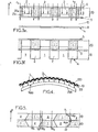
- the pattern of cells in each set may be triangular ( Figure 2a ), square ( Figure 2b ), rectangular, or even random ( Figure 2c ).
- the lateral dimension of the cells 1 parallel to the structure 100 which is also the lateral dimensions of the portions 2, may lie in the range 1 micrometer ( ⁇ m) to 200 ⁇ m, and preferably in the range 5 ⁇ m to 100 ⁇ m. Each cell 1 or portion 2 is then not individually visible to the naked eye and does not give rise to diffraction of light. This lateral dimension is referenced d in Figure 1 .
- Both sets of cells, within the layers 10 and 20 respectively, preferably have filling factors that are substantially identical.
- the term "filling factor" when applied to a set of cells is used to mean the percentage of the area of the structure 100 that is occupied by the cells 1 in the set, within a given layer 10, 20. Given that the patterns in the two sets of cells are complementary, the two filling factors are then both substantially equal to 50%.
- Each cell 1 contains an optically active material.
- the active material may comprise a refringent material, a polarizing material, an absorbing material, a colored material, a filter material, an electroactive material, etc.
- the material is selected in known manner as a function of the optical property that the cell structure 100 is to confer on an optical component with which it is integrated.
- a refringent material may be introduced into the cells 11, which has an optical refractive index that varies between cells that are offset parallel to the structure 100.
- the structure 100 may exhibit a determined optical power expressed in diopters.
- an electroactive material is a material that has a characteristic that can vary in response to an electrical control signal.
- the active material that is contained in at least one of the cells 1 may be a liquid or a gel.
- two external films referenced 4 and 5 can be disposed on either side of the structure 100 to close hermetically the cells 1 of the layers 10, 20. In this way, the active materials that are contained in the various cells 1 are prevented from mixing or leaking away from the structure 100.
- Each film 4, 5 may be bonded to the separating portions 2 of the corresponding layer 10, 20, for example by means of a layer of pressure-sensitive adhesive (PSA) material 6, 7.
- PSA pressure-sensitive adhesive
- a single external film may be placed on one side only of the structure 100, e.g. when the active materials that are contained in the cells 1 of one of the layers 10, 20 are cross-linked after being introduced into the cells.
- the structure 100 may also include an intermediate film 3 disposed between the layers 10 and 20. Such a film 3 can confer improved cohesion to the structure 100, thus making the structure easier to manipulate.
- the structure 100 is made of materials that are transparent so that it is itself transparent for light rays passing through it between its two outside faces.
- the separating portions 2 in at least one of the two layers 10, 20 may be made of resin, and the films 3-5 may be based on polycarbonate (PC), polyethylene (PE), polyimide, or polyethylene terephthalate (PET).
- the films 3-5 may have respective thicknesses on the axis N lying in the range 2 ⁇ m to 50 ⁇ m, and the layers 10, 20 may have respective thicknesses lying in the range 5 ⁇ m to 500 ⁇ m.
- the thicknesses of the layers 10 and 20 are referenced e 1 and e 2 respectively.
- the structure 100 initially comprises, in order along the axis N going upwards in Figure 3a : a layer of lithographic resin 10, an additional layer 21 of a resin that absorbs lithographic radiation usable for etching the layer 10, and another layer of resin 22.
- the layers 21 and 22 together form the layer 20 as described above.
- the layers 10, 21, and 22 are initially homogenous, and they present thicknesses that are uniform. For example, the thickness e 21 of the layer 21 lies in the range 10 ⁇ m to 200 ⁇ m and the thickness e 22 of the layer 22 lies in the range 10 ⁇ m to 400 ⁇ m.
- the structure 100 may optionally initially include the intermediate film 3 located between the layers 10 and 20, and/or a support film 8 that is disposed on a side of the layer 10 opposite from the layer 22.
- the intermediate film 3 is present in the structure 100, it is transparent for the radiation used for lithographically etching the layer 10.
- a mask 30 is then formed on the layer 22.
- the mask 30 may itself be formed by using a lithographic method.
- the mask 30 has openings referenced O, and the layers 22 and then 21 are etched by removing portions thereof through the openings O. In this manner, a first set of cells 1 is formed in the layers 21 and 22, which cells corresponding to the openings O in the mask 30.
- the mask 30 presents a covering factor on the face S2 of the structure 100 that corresponds to the desired filling factor for the cells 1 in the layer 20.
- the covering factor is approximately equal to 50% so as to end up with surface fractions occupied by the cells 1 that are shared in balanced manner between the layers 10 and 20.
- the mask 30 presents a pattern of openings corresponding to the cell pattern desired for the layer 20.
- the openings O may thus exhibit a pattern that is triangular, square, rectangular, or random.
- Two different methods may be used for etching the layers 21 and 22.
- At least the layer 22 is made of lithographic resin and is etched using an appropriate lithographic method.
- radiation F1 ( Figure 3b ), which may be ultraviolet radiation or an electron beam, is directed against the layer 22 through the openings O in the mask 30, in the reverse direction along the axis N.
- the remaining portions of the mask 30 absorb the radiation F1 so that only the uncovered portions of the layer 22 are irradiated. Irradiation causes the resin of the layer 22 to be polymerized or cross-linked in those portions thereof that are uncovered, such that those portions become permanently fixed.
- the layer 22 is then developed: its portions that have not been irradiated are eliminated ( Figure 3c ).
- the layer 22 is a resin negative.
- Developing the lithographic resin of the layer 22 is itself known, and can be performed by putting the layer 22 into contact with a bath for dissolving the non-polymerized resin.
- the portions of the layer 21 that are located in line with the portions that have been eliminated from the layer 22 can be removed simultaneously, e.g. because the same lithographic resin as that used in the layer 22 is a component of material in the layer 21.
- the layer 21 may merely be soluble on coming into contact with a suitable solution at the locations of the portions of the layer 22 that have been removed.
- the uncovered portions of the layer 22 can be removed by being etched using an ion beam.
- This technique of reactive ion etching (RIE) is also known to the person skilled in the art.
- the surface S 2 of the structure 100 is scanned with a beam of ions having energy that is sufficiently high to pulverize the resin in the open zones of the mask 30.
- the layer 21 may optionally be etched simultaneously by the ion beam.
- One or more optically active materials is/then are introduced into the cells 1 of the layer 2 so as to fill them ( Figure 3d ).
- the active materials are liquids or gels
- they can be introduced into the cells 1 by using a spray head, e.g. of the ink jet printer type.
- the head is moved over the surface S 2 and is activated when it is facing a cell so as to spray the active materials therein.
- Filing the cells in this way is particularly rapid and inexpensive, in particular because it can be programmed and it is compatible with using a plurality of active materials for a given cell structure.
- a plurality of active materials can be mixed within a given cell, by introducing appropriate quantities of each material into the cell, using different nozzles of the head, which nozzles are connected to reservoirs of respective active materials.
- the cells 1 filled with active material in the layer 20 can be sealed by means of a film 5 that is fastened on the free surfaces of the separator portions 2.
- the film 5 may be covered by a layer 7 of PSA material and pressed against the faces S 2 of the structure 100, with the layer 7 facing the layer 20.
- other adhesive materials can be used for the layer 7.
- the layer of lithographic resin 10 is then irradiated via the face S 2 , through the layer of cells 20 ( Figure 3e ), so that the portions of the layer 10 that are located in line with the cells 1 of the layer 20 become permanently fixed, selectively compared with the portions of the layer 10 that are located in line with the remaining portions 21a and 22a of the layers 1 and 22.
- radiation F 2 which may be ultraviolet radiation or an electron beam, is directed against the surface S 2 of the structure parallel to the axis N and in the opposite direction thereto.
- the remaining portions 21a of the layer 21 perform the mask function by absorbing the radiation F 2 , so that only those portions of the layer 10 that are located in line with the cells 1 of the layer 20 are irradiated.
- the films 3 and 5 are transparent for the radiation F 2 .
- the structure 100 When the structure 100 includes a support film 8 on its face S 1 , it is removed, e.g. by being peeled off ( Figure 3f ).
- the layer 10 is of negative lithographic resin, possibly identical to that of the layer 22. On being developed, only those portions thereof that have not been irradiated are eliminated. In this way, the separating portions 2 are also created in the layer 10, in line with the cells 1 in the layer 20. These portions 2 of the layer 10 define cells 1 in said layer 10, of outline that coincides with the outline of the portions 2 and of the cells 1 in the layer 20. Thus, the two layers 10 and 20 contain respective sets of cells 1 that are disposed in complementary manner.
- the cells 1 of the layer 10 are filled with optically active material(s) using a method analogous to that already used for the cells 1 of the layer 20.
- the filled cells of the layer 10 are subsequently sealed by applying a second outer film on the face S 1 of the structure 100.
- the structure 100 is turned over during these last two steps so that the cells 1 of the layer 10 are open upwardly.
- the structure 100 then has the configuration shown in Figure 1 .
- a cell structure 100 as proposed by the present invention can then be used for fabricating an optical component, in particular an ophthalmic lens.
- a base optical component 200 ( Figure 4 ) is initially obtained in order to act as a substrate.
- the base component 200 may itself be an optical lens, or an ophthalmic lens.
- ophthalmic lens is used to mean a lens that is designed to be fitted to a frame for a pair of eyeglasses. The lens may be obtained prior to being cut to the dimensions of a housing in the frame. That constitutes an ophthalmic lens blank. Alternatively, it may already be cut to the dimensions of the frame.
- the structure 100 is then fitted onto one of the faces S 200 of the base component 200, while being provided with a curvature identical to that of the face S 200 .
- the structure 100 is deformed with care, using a method that is itself known, so as to avoid crushing or damaging the cells 1 or the separating portions 2 in either of the layers 10 and 20.
- the structure 100 is then fastened on the face S 200 of the base component 200, e.g. by adhesive.
- optical component with cells that is obtained in this way generates reduced diffraction of a light beam passing through it.
- the initial intensity of the beam i.e. its intensity prior to passing through the component
- optical components of the invention have been made in which a fraction of the energy of the incident light beam in excess of 95% is contained in the zero order diffraction, for a direction of incidence that is perpendicular to the surface of the component.
- this fraction remains substantially constant when the two layers 10 and 20 are of identical thicknesses that vary simultaneously.
- Such a component also exhibits chromatic effects that are very small. In particular, practically no iridescence is visible on the component, even when observed at varying angles of incidence.
- the component is thus particularly suitable for numerous applications, and in particular those that have particularly severe requirements in terms of appearance, such as ophthalmic applications.
- the structure 100 may also include functional coatings on at least one of its faces S 1 or S 2 , and in particular on that one of its faces that remains exposed in the final optical component.
- Such functional coatings can be carried by the outer film 4 or 5.
- These may comprise, in particular, an anti-impact coating, an anti-reflection coating, an anti-scratch coating, a dirt-repellent coating, or a combination of some of said coatings.
- the etched resin layer 22 initially may alternatively be made of a positive resin. Under such circumstances, the cells 1 of the layer 20 are formed at the locations of the openings O in the mask 30.
- a first cell 1 and a first separating portion 2 that are adjacent to each other within one of the layers 10, 20 may present an interface I 1 that is oblique relative to the axis N.
- the angles ⁇ 10 and ⁇ 20 relative to the axis N have equal absolute values and opposite orientations.
- Such a cell structure also leads to reduced diffraction, since the light rays passing through the structure parallel to the axis N have identical path lengths through the active material and the material constituting a separating portion, regardless of the offset of the rays relative to the interfaces I 1 and I 2 (see the rays R 1 -R 4 in Figure 5 ).
- the layered structure may be flexible or rigid, planar or curved, and may optionally be used on its own as a separate optical component.
Landscapes
- Physics & Mathematics (AREA)
- Nonlinear Science (AREA)
- Mathematical Physics (AREA)
- Chemical & Material Sciences (AREA)
- Crystallography & Structural Chemistry (AREA)
- General Physics & Mathematics (AREA)
- Optics & Photonics (AREA)
- Laminated Bodies (AREA)
- Optical Elements Other Than Lenses (AREA)
- Polarising Elements (AREA)
- Prostheses (AREA)
Description
- The present invention relates to an optically transparent component having two sets of cells, to a layered structure suitable for use in fabricating such a component, and to methods of fabricating the component and the structure.
- It is known, in particular from patent application
WO 2006/013250 , to make an optical component in the form of a base component that carries, on one of its surfaces, a set of juxtaposed cells. Such a component structure is often referred to as a pixelized structure. The cells contain one or more optically active materials, that confer some particular optical property on the component. Such a method of making optical components is particularly advantageous, because components can be obtained that have differing optical properties by varying the active material that is introduced into the cells. - It is also known to make an optical component that incorporates a plurality of sets of cells situated in respective superposed layers on a surface of a base optical component. The optical component then has a combination of optical properties that are conferred by all the sets of cells.
- However such optical components exhibit transparency that can be insufficient for certain applications, in particular for ophthalmic applications. The separator walls between the cells in a set diffract light. This diffraction itself gives rise to macroscopic diffusion.
- In the meaning of the invention, it is considered that an optical component is transparent when an image that is observed through the component is perceived without significant loss of contrast. In other words, interposing a transparent optical component between an image and an observer of the image does not significantly reduce the quality of the image. In particular, diffraction is defined as being the phenomenon whereby the light that is being observed is scattered when the light ray is physically limited (J-P. Perez, Optique, Fondements et applications [Optics, foundations and applications], 7th edition, DUNOD, October 2004, p. 262). Because of the diffraction by the walls of an optical component having cells, a point of light is no longer perceived as a point when looking through the optical component. The resulting macroscopic diffusion, or incoherent diffusion, produces a milky appearance or diffusion halo, due to the pixelized structure of the optical component. This leads to a loss of contrast in an image that is observed through the component. This loss of contrast is equivalent to a loss of transparency, as defined above.
- An optical component comprising two superposed staggered layers of cells each cell comprising an optical fluid, is known from document
US 2003/0174 385 A1 . - An object of the present invention thus consists in proposing a novel type of optical component having cells, which component has an improved level of transparency.
- For this purpose, the invention proposes a transparent optical component comprising a base optical component and two transparent sets of cells. The cells in the two sets are arranged in respective layers that are superposed on a surface of the base component. Each cell contains an optically active material, and the cells in each set are isolated from one another by separating portions within the corresponding layer, parallel to the surface of the base component. In addition, a cell in either set is located in line with a separating portion pertaining to the layer of the other set of cells, along an axis perpendicular to the surface of the base component. Furthermore, the respective outlines of a cell and of a separating portion located in line with each other have substantially identical projections on the surface of the base component.
- In other words, in the invention, the two sets of cells have cell patterns that are complementary relative to the surface of the optical component. In addition, within each layer, the cells and the separating portions alternate in any direction parallel to the surface of the component, such that two adjacent cells are always disjoint.
- In an optical component of the invention, a light ray that passes through the component substantially perpendicularly to the layers necessarily passes through one cell and one separating portion, regardless of the point of impact of the ray on the surface of the optical component. Depending on the point of impact, the only thing that varies is the order of the cell and the separating portion on the path of the ray. All of the rays of a given light beam thus have optical paths that are substantially equivalent through the optical component, so the component introduces little deformation in an image that is observed therethrough. In other words the component is more transparent in the meaning defined above.
- Because of this equivalence between the paths of light rays passing through the optical component at different locations of the surface carrying the sets of cells, it is not necessary for the separating portions and the active materials that are contained in the cells to have identical refractive indices. Eliminating such an index-matching constraint makes it possible to use identical cell matrices for different optical components, that differ in the active materials that are introduced into the respective cells of the components. The base optical component and the sets of cells can then be produced in large quantities at low cost.
- In addition, in an optical component of the invention, the separating portions between cells have dimensions parallel to the surface of the substrate that are comparable to the dimensions of the cells. They therefore do not give rise to diffraction at an additional scale. The transparency of the component is consequently also improved for this reason.
- Furthermore, because the dimensions of the cells and the dimensions of the separating portions are comparable or identical, both sets of cells can be made easily, in particular by using known lithographic methods.
- Finally, when the cells of at least one of the sets are closed by means of an external film that is applied on the set, the film can easily be fastened on the separating portions of the cells, e.g. by adhesive. Given that the separating portions present respective areas that are large and that are available for fastening the film, it is possible to obtain hermetic and robust sealing of the cells.
- In particular, an optical component of the invention may form an optical lens, in particular an ophthalmic lens. It may also optionally form an element of an optical instrument for measuring or sighting, a lens for goggles, in particular for sporting or protective purposes, a helmet visor, a porthole window, etc.
- The invention also provides a layered transparent cell structure that can be applied on a base optical component to obtain a pixelized component having two layers of cells as described above.
- The invention also provides a method of fabricating such a structure, the method comprising the following steps:
- a) obtaining a transparent structure of superposed layers comprising, in order: a first layer of lithographic resin, an additional layer that is absorbing for a radiation of a lithographic method suitable for etching the first layer of resin, and a second layer;
- b) forming a mask on the second layer, this mask defining the locations of the cells to be formed;
- c) selectively removing portions of the second layer and of the additional layer as defined by the mask so as to form a first set of cells in these layers;
- d) filling the cells of the first set with at least one optically active material;
- e) after the mask has been removed, irradiating the first layer of lithographic resin through the second layer and the additional layer so that the portions of said first layer that are located in line with cells of the first set become permanently fixed, selectively relative to portions of the first layer that are located in line with the remaining portions of the additional layer;
- f) developing the first resin layer so as to form a second set of cells in the first resin layer; and
- g) filling the cells of the second set with an optically active material.
- By using such a method, the two sets of cells are automatically obtained in a manner that is self-aligned and complementary relative to each other, and requiring only one mask to be used. No specific alignment step is therefore needed for obtaining the two superposed layers with the cells in one of the sets being located exactly in line with the separating portions between the cells of the other set. In addition, a cell and a separating portion that are located one over the other automatically have outlines that are identical, parallel to the layer structure.
- Finally, the invention provides a method of fabricating an optical component in which a layered cell structure as described above is fitted on a base optical component. The resulting optical component may be an optical lens, and in particular an ophthalmic lens.
- Other features and advantages of the present invention appear in the following description of nonlimiting embodiments, given with reference to the accompanying drawings, in which:
-
Figure 1 is a section view of a cell structure of the invention; -
Figure 2a-2c are plan views of cell structures in accordance withFigure 1 ; -
Figures 3a-3f show successive steps in a method of fabricating a cell structure in accordance with the preceding figures; -
Figure 4 shows the fabrication of an optical component of the invention; and -
Figure 5 is a section view of a variant configuration of a cell structure of the invention. - For sake clarity in the figures, the dimensions of elements shown are not in proportion with the real dimensions or the real dimension ratios. Furthermore, when identical references are used on different figures they correspond to elements that are identical or that perform identical functions.
- The description begins with a cell structure of the invention, given with reference to
Figures 1 and 2a-2c . - The
structure 100 comprises two sets of cells referenced 1, that are disposed in twolayers layers structure 100 along an axis N perpendicular to the outside faces of thestructure 100, which faces are referenced S1 and S2. Thecells 1 in a given set, i.e. that are located in a givenlayer - In addition, a
cell 1 pertaining to the set of cells in thelayer 10 is located in line with a separatingportion 2 pertaining to thelayer 20, along the axis N. Conversely, acell 1 pertaining to the set of cells of thelayer 20 is located in line with a separatingportion 2 pertaining to thelayer 10. Furthermore, acell 1 and aportion 2 that are located in line with each other have respective outlines that have substantially identical projections on a surface parallel to the faces S1 and S2. - Because of the matching outlines of the cells in the two sets, the
cells 1 of thelayer 10 form a pattern that is complementary to the pattern of thecells 1 of thelayer 20. The pattern of cells in each set may be triangular (Figure 2a ), square (Figure 2b ), rectangular, or even random (Figure 2c ). The lateral dimension of thecells 1 parallel to thestructure 100, which is also the lateral dimensions of theportions 2, may lie in therange 1 micrometer (µm) to 200 µm, and preferably in therange 5 µm to 100 µm. Eachcell 1 orportion 2 is then not individually visible to the naked eye and does not give rise to diffraction of light. This lateral dimension is referenced d inFigure 1 . - Both sets of cells, within the
layers structure 100 that is occupied by thecells 1 in the set, within a givenlayer - Each
cell 1 contains an optically active material. The active material may comprise a refringent material, a polarizing material, an absorbing material, a colored material, a filter material, an electroactive material, etc. The material is selected in known manner as a function of the optical property that thecell structure 100 is to confer on an optical component with which it is integrated. For example, a refringent material may be introduced into the cells 11, which has an optical refractive index that varies between cells that are offset parallel to thestructure 100. Thus, thestructure 100 may exhibit a determined optical power expressed in diopters. Furthermore, in the meaning of the invention, an electroactive material is a material that has a characteristic that can vary in response to an electrical control signal. - The active material that is contained in at least one of the
cells 1 may be a liquid or a gel. Under such circumstances, two external films referenced 4 and 5 can be disposed on either side of thestructure 100 to close hermetically thecells 1 of thelayers various cells 1 are prevented from mixing or leaking away from thestructure 100. Eachfilm portions 2 of thecorresponding layer structure 100, e.g. when the active materials that are contained in thecells 1 of one of thelayers - The
structure 100 may also include anintermediate film 3 disposed between thelayers film 3 can confer improved cohesion to thestructure 100, thus making the structure easier to manipulate. - The
structure 100 is made of materials that are transparent so that it is itself transparent for light rays passing through it between its two outside faces. In particular, the separatingportions 2 in at least one of the twolayers range 2 µm to 50 µm, and thelayers range 5 µm to 500 µm. InFigure 1 , the thicknesses of thelayers - There follows a description of a method of obtaining such a layered cell structure, given with reference to
Figures 3a-3f . - The
structure 100 initially comprises, in order along the axis N going upwards inFigure 3a : a layer oflithographic resin 10, anadditional layer 21 of a resin that absorbs lithographic radiation usable for etching thelayer 10, and another layer ofresin 22. Thelayers layer 20 as described above. Thelayers layer 21 lies in therange 10 µm to 200 µm and the thickness e22 of thelayer 22 lies in therange 10 µm to 400 µm. Thestructure 100 may optionally initially include theintermediate film 3 located between thelayers support film 8 that is disposed on a side of thelayer 10 opposite from thelayer 22. When theintermediate film 3 is present in thestructure 100, it is transparent for the radiation used for lithographically etching thelayer 10. - A
mask 30 is then formed on thelayer 22. In one possibility, themask 30 may itself be formed by using a lithographic method. Themask 30 has openings referenced O, and thelayers 22 and then 21 are etched by removing portions thereof through the openings O. In this manner, a first set ofcells 1 is formed in thelayers mask 30. - The
mask 30 presents a covering factor on the face S2 of thestructure 100 that corresponds to the desired filling factor for thecells 1 in thelayer 20. Preferably, the covering factor is approximately equal to 50% so as to end up with surface fractions occupied by thecells 1 that are shared in balanced manner between thelayers - In the same manner, the
mask 30 presents a pattern of openings corresponding to the cell pattern desired for thelayer 20. In particular, the openings O may thus exhibit a pattern that is triangular, square, rectangular, or random. - Two different methods may be used for etching the
layers - In a first method, at least the
layer 22 is made of lithographic resin and is etched using an appropriate lithographic method. For this reason, radiation F1 (Figure 3b ), which may be ultraviolet radiation or an electron beam, is directed against thelayer 22 through the openings O in themask 30, in the reverse direction along the axis N. The remaining portions of themask 30 absorb the radiation F1 so that only the uncovered portions of thelayer 22 are irradiated. Irradiation causes the resin of thelayer 22 to be polymerized or cross-linked in those portions thereof that are uncovered, such that those portions become permanently fixed. - The remaining portions of the
mask 30 are removed. - The
layer 22 is then developed: its portions that have not been irradiated are eliminated (Figure 3c ). In other words, thelayer 22 is a resin negative. Developing the lithographic resin of thelayer 22 is itself known, and can be performed by putting thelayer 22 into contact with a bath for dissolving the non-polymerized resin. The portions of thelayer 21 that are located in line with the portions that have been eliminated from thelayer 22 can be removed simultaneously, e.g. because the same lithographic resin as that used in thelayer 22 is a component of material in thelayer 21. Alternatively, thelayer 21 may merely be soluble on coming into contact with a suitable solution at the locations of the portions of thelayer 22 that have been removed. - In a second method that is not shown in the figures, the uncovered portions of the
layer 22 can be removed by being etched using an ion beam. This technique of reactive ion etching (RIE) is also known to the person skilled in the art. For this purpose, the surface S2 of thestructure 100 is scanned with a beam of ions having energy that is sufficiently high to pulverize the resin in the open zones of themask 30. Thelayer 21 may optionally be etched simultaneously by the ion beam. - The remaining portions of the
layer 22, referenced 22a inFigure 3c , and those of thelayer 21, referenced 21a, form the separatingportions 2 of thelayer 20, and the empty portions of thelayers cells 1. - One or more optically active materials is/then are introduced into the
cells 1 of thelayer 2 so as to fill them (Figure 3d ). When the active materials are liquids or gels, they can be introduced into thecells 1 by using a spray head, e.g. of the ink jet printer type. The head is moved over the surface S2 and is activated when it is facing a cell so as to spray the active materials therein. Filing the cells in this way is particularly rapid and inexpensive, in particular because it can be programmed and it is compatible with using a plurality of active materials for a given cell structure. In addition, a plurality of active materials can be mixed within a given cell, by introducing appropriate quantities of each material into the cell, using different nozzles of the head, which nozzles are connected to reservoirs of respective active materials. - Optionally, the
cells 1 filled with active material in thelayer 20 can be sealed by means of afilm 5 that is fastened on the free surfaces of theseparator portions 2. For example, thefilm 5 may be covered by a layer 7 of PSA material and pressed against the faces S2 of thestructure 100, with the layer 7 facing thelayer 20. As an alternative, other adhesive materials can be used for the layer 7. - The layer of
lithographic resin 10 is then irradiated via the face S2, through the layer of cells 20 (Figure 3e ), so that the portions of thelayer 10 that are located in line with thecells 1 of thelayer 20 become permanently fixed, selectively compared with the portions of thelayer 10 that are located in line with the remainingportions layers portions 21a of thelayer 21 perform the mask function by absorbing the radiation F2, so that only those portions of thelayer 10 that are located in line with thecells 1 of thelayer 20 are irradiated. For this purpose, thefilms - When the
structure 100 includes asupport film 8 on its face S1, it is removed, e.g. by being peeled off (Figure 3f ). - The
layer 10 is of negative lithographic resin, possibly identical to that of thelayer 22. On being developed, only those portions thereof that have not been irradiated are eliminated. In this way, the separatingportions 2 are also created in thelayer 10, in line with thecells 1 in thelayer 20. Theseportions 2 of thelayer 10 definecells 1 in saidlayer 10, of outline that coincides with the outline of theportions 2 and of thecells 1 in thelayer 20. Thus, the twolayers cells 1 that are disposed in complementary manner. - Finally, the
cells 1 of thelayer 10 are filled with optically active material(s) using a method analogous to that already used for thecells 1 of thelayer 20. Optionally, the filled cells of thelayer 10 are subsequently sealed by applying a second outer film on the face S1 of thestructure 100. Advantageously, thestructure 100 is turned over during these last two steps so that thecells 1 of thelayer 10 are open upwardly. Thestructure 100 then has the configuration shown inFigure 1 . - A
cell structure 100 as proposed by the present invention can then be used for fabricating an optical component, in particular an ophthalmic lens. To this end, a base optical component 200 (Figure 4 ), is initially obtained in order to act as a substrate. Thebase component 200 may itself be an optical lens, or an ophthalmic lens. The term "ophthalmic lens" is used to mean a lens that is designed to be fitted to a frame for a pair of eyeglasses. The lens may be obtained prior to being cut to the dimensions of a housing in the frame. That constitutes an ophthalmic lens blank. Alternatively, it may already be cut to the dimensions of the frame. Thestructure 100 is then fitted onto one of the faces S200 of thebase component 200, while being provided with a curvature identical to that of the face S200. For this purpose, thestructure 100 is deformed with care, using a method that is itself known, so as to avoid crushing or damaging thecells 1 or the separatingportions 2 in either of thelayers structure 100 is then fastened on the face S200 of thebase component 200, e.g. by adhesive. - The optical component with cells that is obtained in this way generates reduced diffraction of a light beam passing through it. In other words, the initial intensity of the beam, i.e. its intensity prior to passing through the component, is to be found almost entirely in the zero order of diffraction after passing through the component. In particular, optical components of the invention have been made in which a fraction of the energy of the incident light beam in excess of 95% is contained in the zero order diffraction, for a direction of incidence that is perpendicular to the surface of the component. In addition, this fraction remains substantially constant when the two
layers - Such a component also exhibits chromatic effects that are very small. In particular, practically no iridescence is visible on the component, even when observed at varying angles of incidence. The component is thus particularly suitable for numerous applications, and in particular those that have particularly severe requirements in terms of appearance, such as ophthalmic applications.
- Naturally, numerous adaptations of the invention can be introduced compared with the embodiment described above. In particular, the
structure 100 may also include functional coatings on at least one of its faces S1 or S2, and in particular on that one of its faces that remains exposed in the final optical component. Such functional coatings can be carried by theouter film - In addition, the etched
resin layer 22 initially may alternatively be made of a positive resin. Under such circumstances, thecells 1 of thelayer 20 are formed at the locations of the openings O in themask 30. - In a variant embodiment of the invention, shown in
Figure 5 , afirst cell 1 and afirst separating portion 2 that are adjacent to each other within one of thelayers Figure 5 ). - Finally, the layered structure may be flexible or rigid, planar or curved, and may optionally be used on its own as a separate optical component.
Claims (31)
- A transparent optical component forming an optical lens or an ophthalmic lens, and comprising a base optical component (200) and two transparent sets of cells (1) arranged in respective layers (10, 20) superposed on a surface of said base component, each cell (1) containing an optically active material, and the cells in each set being isolated from one another by separating portions (2) within the corresponding layer, parallel to the surface of the base component, the component being characterized in that a cell (1) in each set is located in line with a separating portion (2) pertaining to the other set of cells, along an axis (N) perpendicular to the surface of the base component, with respective outlines for said cell and said separating portion that have substantially identical projections on the surface of the base component.
- The component according to claim 1, in which the sets of cells (1) have filling factors that are substantially identical within the respective layers.
- The component according to claim 1 or claim 2, in which the sets of cells (1) have respective patterns that are triangular, square, rectangular, or random within the respective layers.
- The component according to any one of the preceding claims, in which the separating portions (2) are of resin in at least one of the layers.
- The component according to any one of the preceding claims, further comprising an intermediate film (3) disposed between the respective layers of the two sets of cells (10, 20).
- The component according to any one of the preceding claims, further comprising at least one external film (4, 5) disposed on a side of one of the layers of set of cells (10, 20) that is opposite from the side on which the other layer of set of cells is disposed.
- The component according to any one of the preceding claims, in which the optically active material contained in at least one of the cells comprises a refringent material, a polarizing material, an absorbing material, a colored material, a filter material, or an electroactive material.
- The component according to any one of the preceding claims, in which the optically active material contained in at least one of the cells (1) is a liquid or a gel.
- The component according to any one of the preceding claims, in which a first cell (1) and a first separating portion (2) that are adjacent within one of the layers (10) have a first interface (I1) that is oblique relative to a direction perpendicular to the surface of the optical component (N), and in which a second cell (1) and a second separating portion (2) adjacent to each other and forming part of the other layer (20), and being located in line with said first separating portion and first cell, respectively, have a second interface (I2) that is inclined oppositely relative to said first interface.
- The component according to any one of the preceding claims, in which the base optical component (200) itself comprises an optical lens.
- A layered transparent cellular structure (100) suitable for being peeled of from a support film (8) and fabricating a transparent optical component forming an optical lens or an ophthalmic lens when fitted onto one of the faces of a base component (200), the structure comprising two sets of cells (1) arranged in respective superposed layers (10, 20) in said structure, each cell (1) containing an optically active material, and the cells of each set being isolated from one another by separating portions (2) within the corresponding layer in directions that are parallel to the layer structure, the structure (100) being characterized in that a cell (1) of each set is located in line with a separating portion (2) pertaining to the layer of the other set of cells, along an axis (N) perpendicular to the cell structure, with respective outlines for said cell and said separating portion that have substantially identical projections on a surface parallel to the layered structure.
- The structure according to claim 11, in which the sets of cells (1) have substantially identical filling factors within the respective layers.
- The structure according to claim 11 or claim 12, in which the sets of cells (1) have respective patterns that are triangular, square, rectangular, or random within the respective layers.
- The structure according to any one of claims 11 to 13, in which the separating portions (2) are made of resin in at one of the layers of the structure.
- The structure according to any one of claims 11 to 14, further comprising an intermediate film (3) disposed between the respective layers of the two sets (10, 20) of cells.
- The structure according to any one of claims 11 to 15, further comprising at least one external film (4, 5) disposed on a side of one of the layers of set (10, 20) of cells that is opposite from the side on which the other layer of set of cells is disposed.
- The structure according to any one of claims 11 to 16, in which the optically active material contained in at least one of the cells (1) comprises a refringent material, a polarizing material, an absorbing material, a colored material, a filter material, or an electroactive material.
- The structure according to any one of claims 11 to 17, in which the optically active material contained in at least one of the cells (1) is a liquid or a gel.
- The structure according to any one of claims 11 to 18, in which a first cell (1) and a first separating portion (2) that are adjacent within one of the layers (10) have a first interface (I1) that is oblique relative to an axis (N) perpendicular to the structure, and in which a second cell (1) and a second separator portion (2) that are adjacent to each other and form part of the other layer (20), and being located in line with said first separating portion and said first cell, respectively, have a second interface (I2) that is inclined oppositely relative to said first interface.
- A method of fabricating a layered transparent cell structure (100) suitable for being fastened onto an optical lens or an ophthalmic lens, the method comprising the following steps:a) obtaining a transparent structure of superposed layers comprising, in order: a first layer (10) of lithographic resin, an additional layer (21) that is absorbing for a radiation of a lithographic method suitable for etching the first layer of resin, and a second layer (22);b) forming a mask (30) on said second layer (22), said mask defining the locations of cells (1) to be formed;c) selectively removing portions of said second layer (22) and of the additional layer (21) as defined by the mask (30) so as to form a first set of cells (1) in said second layer and in said additional layer;d) filling the cells (1) of the first set with at least one optically active material;e) after the mask (30) has been removed, irradiating the first layer of lithographic resin (10) through the second layer (22) and the additional layer (21) so that portions of said first layer that are located in line with cells (1) of the first set become permanently fixed, selectively relative to portions of said first layer (10) that are located in line with remaining portions of the additional layer (21a);f) developing the first resin layer (10) so as to form a second set of cells (1) in said first resin layer; andg) filling the cells (1) of the second set with optically active material.
- The method according to claim 20, in which the second layer (22) is made of lithographic resin, and in which step c) is performed using a lithographic method.
- The method according to claim 20, in which step c) is performed by etching the second layer (22) with an ion beam.
- The method according to any one of claims 20 to 22, in which the mask (30) has a covering factor with the second layer (22) that is approximately equal to 50%.
- The method according to any one of claims 20 to 23, in which the mask (30) has a pattern that is triangular, square, rectangular, or random.
- The method according to any one of claims 20 to 24, in which the layered structure (100) further includes an intermediate film (3) situated between said first layer (10) and said additional layer (21).
- The method according to any one of claims 20 to 25, in which the layered structure (100) initially further comprises a support film (8) disposed on a side of the first resin layer (10) opposite from its side on which the second layer (22) is disposed, and in which the method further includes a step of removing said support film, which step of removing is performed before step f).
- The method according to any one of claims 20 to 26, further including at least one step of closing the cells (1) of one of the first and second sets of cells by means of an external film (4, 5) fastened on said set of cells.
- The method according to any one of claims 20 to 27, in which the optically active material used in steps d) and g) comprises a refringent material, a polarizing material, an absorbing material, a colored material, a filter material, or an electroactive material.
- The method according to any one of claims 20 to 28, in which the optically active material used in steps d) and g) is a liquid or a gel.
- A method of fabricating a transparent optical component, the method comprising the following steps:· obtaining a base optical component (200);· obtaining a layered transparent cellular structure (100) according to any one of claims 11 to 19; and· fastening the layered structure on a surface (S200) of the base optical component (200),wherein the transparent optical component forms an optical lens or an ophthalmic lens.
- The method according to claim 30, in which the base optical component (200) itself comprises an optical lens.
Applications Claiming Priority (2)
| Application Number | Priority Date | Filing Date | Title |
|---|---|---|---|
| FR0611377A FR2910642B1 (en) | 2006-12-26 | 2006-12-26 | TRANSPARENT OPTICAL COMPONENT WITH TWO CELL ARRAYS |
| PCT/EP2007/064336 WO2008077880A1 (en) | 2006-12-26 | 2007-12-20 | Optically transparent component with two sets of cells |
Publications (2)
| Publication Number | Publication Date |
|---|---|
| EP2097784A1 EP2097784A1 (en) | 2009-09-09 |
| EP2097784B1 true EP2097784B1 (en) | 2012-11-28 |
Family
ID=38223228
Family Applications (1)
| Application Number | Title | Priority Date | Filing Date |
|---|---|---|---|
| EP20070857956 Active EP2097784B1 (en) | 2006-12-26 | 2007-12-20 | Optically transparent component with two sets of cells |
Country Status (8)
| Country | Link |
|---|---|
| US (1) | US8331007B2 (en) |
| EP (1) | EP2097784B1 (en) |
| JP (1) | JP5395673B2 (en) |
| KR (1) | KR101423619B1 (en) |
| CN (2) | CN102681209B (en) |
| FR (1) | FR2910642B1 (en) |
| TW (1) | TWI439719B (en) |
| WO (1) | WO2008077880A1 (en) |
Families Citing this family (7)
| Publication number | Priority date | Publication date | Assignee | Title |
|---|---|---|---|---|
| FR2972814B1 (en) * | 2011-03-16 | 2014-04-18 | Essilor Int | TRANSPARENT OPTICAL ELEMENT WITH SEVERAL LAYERS CONSISTING OF CELLULAR PAVAGES |
| TWI461810B (en) * | 2011-09-28 | 2014-11-21 | Structure of electronic paper and method of manufacturing the same | |
| DE102012013683B4 (en) * | 2012-07-11 | 2021-04-29 | Carl Zeiss Vision International Gmbh | Spectacle lens, method for the production thereof, computer program and device for the production of a spectacle lens |
| EP2706396A1 (en) | 2012-09-06 | 2014-03-12 | ESSILOR INTERNATIONAL (Compagnie Générale d'Optique) | Method for adapting the optical function of an adaptive ophtalmic lenses system |
| US9442306B1 (en) | 2015-08-17 | 2016-09-13 | Ripclear Llc | Lens protection systems |
| EP3273292A1 (en) * | 2016-07-19 | 2018-01-24 | Carl Zeiss Vision International GmbH | Spectacle glass and method for its production |
| WO2018193057A1 (en) * | 2017-04-20 | 2018-10-25 | Essilor International | Optical device adapted to be worn by a wearer |
Family Cites Families (112)
| Publication number | Priority date | Publication date | Assignee | Title |
|---|---|---|---|---|
| US2196066A (en) | 1938-03-02 | 1940-04-02 | Feinbloom William | Contact lens |
| US2511329A (en) | 1946-12-26 | 1950-06-13 | Craig Edward | Lens shield |
| US3460960A (en) | 1965-05-03 | 1969-08-12 | Owens Illinois Inc | Coated glass and method of making same |
| US3532038A (en) | 1967-06-05 | 1970-10-06 | Ibm | Multi-lens devices for the fabrication of semiconductor devices |
| US3628854A (en) | 1969-12-08 | 1971-12-21 | Optical Sciences Group Inc | Flexible fresnel refracting membrane adhered to ophthalmic lens |
| US3978580A (en) | 1973-06-28 | 1976-09-07 | Hughes Aircraft Company | Method of fabricating a liquid crystal display |
| US4150878A (en) | 1974-04-05 | 1979-04-24 | Giorgio Barzilai | Hollow-space cell and method for its manufacture |
| US4268132A (en) | 1979-09-24 | 1981-05-19 | Neefe Charles W | Oxygen generating contact lens |
| CH666560A5 (en) | 1983-03-01 | 1988-07-29 | Tadeusz Bobak | DISPLAY DEVICE. |
| JPS60188925A (en) | 1984-03-09 | 1985-09-26 | Canon Inc | Manufacturing method of optical modulation element |
| US4601545A (en) | 1984-05-16 | 1986-07-22 | Kern Seymour P | Variable power lens system |
| JPS61140920A (en) * | 1984-12-13 | 1986-06-28 | Olympus Optical Co Ltd | Liquid crystal lens |
| US4621912A (en) | 1985-02-14 | 1986-11-11 | Meyer Donald R | Foraminated optical contact lens |
| IT1190508B (en) | 1986-03-24 | 1988-02-16 | Daniele Senatore | ADJUSTABLE TRANSPARENCY GLASSES |
| US5017000A (en) | 1986-05-14 | 1991-05-21 | Cohen Allen L | Multifocals using phase shifting |
| IL85860A (en) | 1988-03-24 | 1992-06-21 | Amir Cohen | Contact lens |
| US4994664A (en) | 1989-03-27 | 1991-02-19 | Massachusetts Institute Of Technology | Optically coupled focal plane arrays using lenslets and multiplexers |
| FR2647789B1 (en) | 1989-06-05 | 1994-07-22 | Essilor Int | INDOLINO-SPIRO-OXAZINE PHOTOCHROMIC COMPOUNDS, PROCESS FOR THEIR PREPARATION, PHOTOCHROMIC COMPOSITIONS AND ARTICLES CONTAINING SUCH COMPOUNDS |
| FR2670210A1 (en) | 1990-12-06 | 1992-06-12 | Essilor Int | NOVEL PHOTOCHROMIC COMPOUNDS OF THE INDOLINO-SPIRO-BENZOXAZINE TYPE AND THEIR PREPARATION PROCESS. |
| US5359444A (en) | 1992-12-24 | 1994-10-25 | Motorola, Inc. | Auto-focusing optical apparatus |
| US5576870A (en) | 1993-04-23 | 1996-11-19 | Matsushita Electric Industrial Co., Ltd. | Liquid crystal display panel having a phase grating formed of liquid crystal molecules |
| FR2712593B1 (en) | 1993-11-17 | 1996-01-05 | Essilor Int | New spirooxazines and their use in the field of ophthalmic optics. |
| US5585968A (en) | 1993-12-01 | 1996-12-17 | International Business Machines Corporation | Optical elements having regions of different indices of refraction and method of fabricating the same |
| FR2718447B1 (en) | 1994-04-06 | 1996-05-24 | Essilor Int | Chromenes of the 2,2-diphenyl type heteroannelated in 6.7 and their use in the field of ophthalmic optics. |
| FR2718446B1 (en) | 1994-04-06 | 1997-01-03 | Essilor Int | Heteroannelated Spiro [fluorene- [2H] -benzopyranes] and their use in the field of ophthalmic optics. |
| US5699142A (en) | 1994-09-01 | 1997-12-16 | Alcon Laboratories, Inc. | Diffractive multifocal ophthalmic lens |
| FR2731081B1 (en) | 1995-02-27 | 1997-04-11 | Essilor Int | PROCESS FOR OBTAINING A TRANSPARENT ARTICLE WITH A REFRACTION INDEX |
| US6707516B1 (en) | 1995-05-23 | 2004-03-16 | Colorlink, Inc. | Single-panel field-sequential color display systems |
| US6274288B1 (en) | 1995-06-12 | 2001-08-14 | California Institute Of Technology | Self-trapping and self-focusing of optical beams in photopolymers |
| FR2740231B1 (en) | 1995-10-20 | 1998-03-06 | Christian Dalloz Sa | DRAFT FOR NON-CORRECTOR EYEPIECE |
| US5905561A (en) | 1996-06-14 | 1999-05-18 | Pbh, Inc. | Annular mask lens having diffraction reducing edges |
| US5733077A (en) | 1996-07-02 | 1998-03-31 | The Hilsinger Company Lp | Lens drill guide |
| GB2347005B (en) | 1996-07-26 | 2000-10-04 | Sharp Kk | Methods of filling liquid crystal device |
| US5774273A (en) | 1996-08-23 | 1998-06-30 | Vari-Lite, Inc. | Variable-geometry liquid-filled lens apparatus and method for controlling the energy distribution of a light beam |
| US5812235A (en) | 1996-09-04 | 1998-09-22 | Pemrable Technologies Inc. | Multifocal corneal contact lenses |
| US5763054A (en) | 1996-09-13 | 1998-06-09 | Trw Inc. | Anti-reflection treatment for optical elements |
| US5764333A (en) | 1997-02-27 | 1998-06-09 | Somsel; John R. | Sunshields for eyeglasses |
| DE19714434A1 (en) * | 1997-04-08 | 1998-10-15 | Armin Schaeuble | Selective electronic photo-protective spectacles |
| FR2763070B1 (en) | 1997-05-06 | 1999-07-02 | Essilor Int | NOVEL SPIROOXAZINE PHOTOCHROMIC COMPOUNDS, THEIR USE IN THE FIELD OF OPHTHALMIC OPTICS |
| US5914802A (en) | 1997-07-18 | 1999-06-22 | Northrop Grumman Corporation | Combined spatial light modulator and phase mask for holographic storage system |
| US6262789B1 (en) | 1998-11-27 | 2001-07-17 | Zvi Yaniv | Liquid display and method of making same |
| US6554424B1 (en) | 1999-03-01 | 2003-04-29 | Boston Innovative Optices, Inc. | System and method for increasing the depth of focus of the human eye |
| AU2830200A (en) | 1999-03-05 | 2000-09-28 | Seiko Epson Corporation | Electrophoresis display and its production method |
| WO2000060410A1 (en) | 1999-04-06 | 2000-10-12 | E Ink Corporation | Microcell electrophoretic displays |
| US6871951B2 (en) | 2000-06-23 | 2005-03-29 | E-Vision, Llc | Electro-optic lens with integrated components |
| US6619799B1 (en) * | 1999-07-02 | 2003-09-16 | E-Vision, Llc | Optical lens system with electro-active lens having alterably different focal lengths |
| DE19927361A1 (en) | 1999-06-16 | 2000-12-21 | Creavis Tech & Innovation Gmbh | Electrophoretic displays |
| FR2795361B1 (en) | 1999-06-22 | 2001-09-07 | Essilor Int | OPHTHALMIC LENS MOLDING PROCESS |
| US6309803B1 (en) | 1999-07-01 | 2001-10-30 | Lumenon, Innovative Lightwave Technology, Inc. | On-substrate cleaving of sol-gel waveguide |
| JP2003504349A (en) | 1999-07-08 | 2003-02-04 | エシロール アテルナジオナール カンパニー ジェネラーレ デ オプティック | Bi- or terthienyl-substituted photochromic naphtho [2,1-b] pyran compounds |
| US6781666B2 (en) | 1999-07-16 | 2004-08-24 | Minolta Co., Ltd. | Liquid crystal display and method to manufacture the same |
| US6307243B1 (en) | 1999-07-19 | 2001-10-23 | Micron Technology, Inc. | Microlens array with improved fill factor |
| US6199986B1 (en) | 1999-10-21 | 2001-03-13 | University Of Rochester | Rapid, automatic measurement of the eye's wave aberration |
| US6930818B1 (en) * | 2000-03-03 | 2005-08-16 | Sipix Imaging, Inc. | Electrophoretic display and novel process for its manufacture |
| US6577434B2 (en) | 2000-01-14 | 2003-06-10 | Minolta Co., Ltd. | Variable focal position spatial modulation device |
| US6281366B1 (en) | 2000-02-29 | 2001-08-28 | Essilor International Compagnie Generale D'optique | Photochromic [3H]naphtho[2,1-b]pyran compounds containing an acetylenic substituent, process for their manufacture, and photochromic materials and articles obtained |
| US6545797B2 (en) * | 2001-06-11 | 2003-04-08 | Sipix Imaging, Inc. | Process for imagewise opening and filling color display components and color displays manufactured thereof |
| US6829078B2 (en) | 2000-03-03 | 2004-12-07 | Sipix Imaging Inc. | Electrophoretic display and novel process for its manufacture |
| EP1266256B1 (en) | 2000-03-20 | 2006-06-21 | California Institute of Technology | Application of wavefront sensor to lenses capable of post-fabrication power modification |
| JP4116224B2 (en) | 2000-03-23 | 2008-07-09 | ローム株式会社 | Manufacturing method of lens array |
| US6301051B1 (en) | 2000-04-05 | 2001-10-09 | Rockwell Technologies, Llc | High fill-factor microlens array and fabrication method |
| JP4006925B2 (en) | 2000-05-30 | 2007-11-14 | セイコーエプソン株式会社 | Method for manufacturing electrophoretic display device |
| US6485599B1 (en) | 2000-07-11 | 2002-11-26 | International Business Machines Corporation | Curing of sealants using multiple frequencies of radiation |
| US6813082B2 (en) | 2000-11-27 | 2004-11-02 | Ophthonix, Inc. | Wavefront aberrator and method of manufacturing |
| US7293871B2 (en) | 2000-11-27 | 2007-11-13 | Ophthonix, Inc. | Apparatus and method of correcting higher-order aberrations of the human eye |
| EP1225458B8 (en) | 2001-01-19 | 2007-05-09 | Centre National De La Recherche Scientifique (Cnrs) | Method for the manufacturing of a multilayer guided-wave device on a substrate, and guided-wave device obtained therewith |
| JP2004537061A (en) | 2001-02-07 | 2004-12-09 | コーニング インコーポレイテッド | High contrast screen with random microlens array |
| TW556044B (en) * | 2001-02-15 | 2003-10-01 | Sipix Imaging Inc | Process for roll-to-roll manufacture of a display by synchronized photolithographic exposure on a substrate web |
| WO2002067020A2 (en) | 2001-02-19 | 2002-08-29 | Koninklijke Philips Electronics N.V. | Optical element and method of manufacturing such an optical element |
| US6753067B2 (en) | 2001-04-23 | 2004-06-22 | Sipix Imaging, Inc. | Microcup compositions having improved flexure resistance and release properties |
| US7184066B2 (en) | 2001-05-09 | 2007-02-27 | Clairvoyante, Inc | Methods and systems for sub-pixel rendering with adaptive filtering |
| KR100701442B1 (en) | 2001-05-10 | 2007-03-30 | 엘지.필립스 엘시디 주식회사 | Inkjet liquid crystal coating method |
| US7205355B2 (en) * | 2001-06-04 | 2007-04-17 | Sipix Imaging, Inc. | Composition and process for the manufacture of an improved electrophoretic display |
| US20020188053A1 (en) * | 2001-06-04 | 2002-12-12 | Sipix Imaging, Inc. | Composition and process for the sealing of microcups in roll-to-roll display manufacturing |
| US7217375B2 (en) | 2001-06-04 | 2007-05-15 | Ophthonix, Inc. | Apparatus and method of fabricating a compensating element for wavefront correction using spatially localized curing of resin mixtures |
| US6788452B2 (en) * | 2001-06-11 | 2004-09-07 | Sipix Imaging, Inc. | Process for manufacture of improved color displays |
| US6982178B2 (en) | 2002-06-10 | 2006-01-03 | E Ink Corporation | Components and methods for use in electro-optic displays |
| TW527529B (en) | 2001-07-27 | 2003-04-11 | Sipix Imaging Inc | An improved electrophoretic display with color filters |
| CN1539092A (en) | 2001-08-07 | 2004-10-20 | 金炯植 | Lens holder for rimless glasses |
| TW539928B (en) | 2001-08-20 | 2003-07-01 | Sipix Imaging Inc | An improved transflective electrophoretic display |
| US6712466B2 (en) | 2001-10-25 | 2004-03-30 | Ophthonix, Inc. | Eyeglass manufacturing method using variable index layer |
| TW574566B (en) | 2001-10-31 | 2004-02-01 | Optrex Kk | Liquid crystal display element |
| KR100954016B1 (en) | 2002-01-23 | 2010-04-20 | 소니 주식회사 | Image display element and image projector device |
| US6860601B2 (en) | 2002-02-06 | 2005-03-01 | John H. Shadduck | Adaptive optic lens system and method of use |
| US6963435B2 (en) | 2002-03-27 | 2005-11-08 | Avery Dennison Corporation | Switchable electro-optical laminates |
| US6836371B2 (en) | 2002-07-11 | 2004-12-28 | Ophthonix, Inc. | Optical elements and methods for making thereof |
| US6966649B2 (en) | 2002-08-12 | 2005-11-22 | John H Shadduck | Adaptive optic lens system and method of use |
| US7036932B2 (en) | 2002-10-04 | 2006-05-02 | Vision-Ease Lens | Laminated functional wafer for plastic optical elements |
| EP1563337A4 (en) | 2002-11-20 | 2006-05-24 | Powervision | Lens system and method for power adjustment |
| US20040120667A1 (en) | 2002-12-23 | 2004-06-24 | Eastman Kodak Company | Walled network optical component |
| US6914658B2 (en) | 2002-12-26 | 2005-07-05 | Intel Corporation | Method for fabricating a moat around an active pixel area of a microelectronic image projection device |
| JP2004301878A (en) * | 2003-03-28 | 2004-10-28 | Fujitsu Display Technologies Corp | Liquid crystal display |
| KR20060034700A (en) | 2003-07-14 | 2006-04-24 | 코닌클리케 필립스 일렉트로닉스 엔.브이. | Variable lens |
| DE602004004415T2 (en) | 2003-10-03 | 2007-10-18 | Invisia Ltd. | MULTIFOCAL LENS |
| US7227692B2 (en) | 2003-10-09 | 2007-06-05 | Micron Technology, Inc | Method and apparatus for balancing color response of imagers |
| WO2005072039A1 (en) | 2004-01-21 | 2005-08-04 | Dai Nippon Printing Co., Ltd. | Front plate for display panel and method of producing the same |
| US7036929B1 (en) | 2004-04-12 | 2006-05-02 | William Rolf Harvey | Method and device for the application and removal of disposable corrective optical film to an eyeglass lens |
| FR2872589B1 (en) | 2004-07-02 | 2006-10-27 | Essilor Int | METHOD FOR PRODUCING A TRANSPARENT OPTICAL ELEMENT, OPTICAL COMPONENT INVOLVED IN THIS METHOD AND OPTICAL ELEMENT THUS OBTAINED |
| ES2552373T3 (en) * | 2004-07-02 | 2015-11-27 | Essilor International (Compagnie Générale d'Optique) | Photochromic optical component |
| US7371804B2 (en) | 2004-09-07 | 2008-05-13 | Ophthonix, Inc. | Monomers and polymers for optical elements |
| BRPI0518058A (en) * | 2004-11-02 | 2008-10-28 | E-Vision Llc | electro-spectacles and manufacturing methods |
| FR2879757B1 (en) | 2004-12-17 | 2007-07-13 | Essilor Int | METHOD FOR PRODUCING A TRANSPARENT OPTICAL ELEMENT, OPTICAL COMPONENT INVOLVED IN THIS METHOD AND OPTICAL ELEMENT THUS OBTAINED |
| DE102004062277B4 (en) * | 2004-12-23 | 2021-08-26 | Rodenstock Gmbh | Spectacle lens device with electroadaptive range, spectacles, use and method for operating the spectacle lens device |
| US7533453B2 (en) | 2005-01-24 | 2009-05-19 | Yancy Virgil T | E-facet optical lens |
| FR2883984B1 (en) | 2005-04-04 | 2007-06-22 | Essilor Int | APPARATUS FOR CONFORMING PLANAR FILM TO AN OPTICAL LENS, METHODS OF FUNCTIONALIZING AN OPTICAL LENS USING THE SAME, AND LENS OBTAINED THEREBY |
| US7757629B2 (en) * | 2005-04-14 | 2010-07-20 | Transitions Optical, Inc. | Method and apparatus for coating an optical article |
| FR2888947B1 (en) | 2005-07-20 | 2007-10-12 | Essilor Int | OPTICAL CELL COMPONENT |
| FR2888950B1 (en) | 2005-07-20 | 2007-10-12 | Essilor Int | TRANSPARENT PIXELLIZED OPTICAL COMPONENT WITH ABSORBENT WALLS ITS MANUFACTURING METHOD AND USE IN FARICATION OF A TRANSPARENT OPTICAL ELEMENT |
| FR2888951B1 (en) | 2005-07-20 | 2008-02-08 | Essilor Int | RANDOMIZED PIXELLIZED OPTICAL COMPONENT, METHOD FOR MANUFACTURING THE SAME, AND USE THEREOF IN THE MANUFACTURE OF A TRANSPARENT OPTICAL ELEMENT |
| US7715107B2 (en) | 2006-04-25 | 2010-05-11 | Asml Netherlands B.V. | Optical element for correction of aberration, and a lithographic apparatus comprising same |
| FR2902105B1 (en) | 2006-06-13 | 2008-09-12 | Essilor Int | METHOD FOR BONDING A FILM TO A CURVED SUBSTRATE |
| FR2907559B1 (en) * | 2006-10-19 | 2009-02-13 | Essilor Int | ELECRO-COMMANDABLE OPTICAL COMPONENT COMPRISING A SET OF CELLS |
-
2006
- 2006-12-26 FR FR0611377A patent/FR2910642B1/en active Active
-
2007
- 2007-12-20 KR KR1020097015621A patent/KR101423619B1/en active Active
- 2007-12-20 EP EP20070857956 patent/EP2097784B1/en active Active
- 2007-12-20 CN CN201210124170.1A patent/CN102681209B/en active Active
- 2007-12-20 JP JP2009543451A patent/JP5395673B2/en active Active
- 2007-12-20 WO PCT/EP2007/064336 patent/WO2008077880A1/en not_active Ceased
- 2007-12-20 CN CN2007800517779A patent/CN101652701B/en active Active
- 2007-12-20 US US12/521,312 patent/US8331007B2/en active Active
- 2007-12-26 TW TW96150394A patent/TWI439719B/en not_active IP Right Cessation
Also Published As
| Publication number | Publication date |
|---|---|
| US8331007B2 (en) | 2012-12-11 |
| KR101423619B1 (en) | 2014-07-28 |
| US20110043925A1 (en) | 2011-02-24 |
| FR2910642B1 (en) | 2009-03-06 |
| TW200835929A (en) | 2008-09-01 |
| TWI439719B (en) | 2014-06-01 |
| CN101652701A (en) | 2010-02-17 |
| JP5395673B2 (en) | 2014-01-22 |
| CN101652701B (en) | 2013-02-20 |
| CN102681209B (en) | 2014-06-18 |
| FR2910642A1 (en) | 2008-06-27 |
| CN102681209A (en) | 2012-09-19 |
| JP2010515091A (en) | 2010-05-06 |
| WO2008077880A1 (en) | 2008-07-03 |
| EP2097784A1 (en) | 2009-09-09 |
| KR20090122189A (en) | 2009-11-26 |
Similar Documents
| Publication | Publication Date | Title |
|---|---|---|
| US8331007B2 (en) | Optically transparent component with two sets of cells | |
| KR101234173B1 (en) | Method for producing a transparent optical element, an optical component involved into said method and the thus obtained optical element | |
| RU2571441C2 (en) | Laminated structure with internal cavities to be used with photocells, and its manufacturing method | |
| JP4880702B2 (en) | Lenticular lens array element | |
| CN104977773B (en) | Surface floating type liquid crystal column lens array device, manufacturing method and display device | |
| US20090316110A1 (en) | Method for making a transparent optical element, optical component used in said method and resulting optical element | |
| US20090195883A1 (en) | Optical Element Comprising Cells Sealed by Means of a Layer of Adhesive Material | |
| US8231217B2 (en) | Pixellized transparent optical component comprising an absorbing coating, production method thereof and use thereof in an optical element | |
| KR20070110245A (en) | Light collimation device | |
| KR20080040719A (en) | Pixelated transparent optical parts with absorbent walls, methods for their preparation and use thereof in the manufacture of transparent optical devices | |
| CN110568616B (en) | Method for providing a head-mounted optical system | |
| JP5137830B2 (en) | Pixelated optical component with apodized walls, method of manufacturing the optical component, and use of the optical component in the manufacture of transparent optical elements | |
| TWI805750B (en) | Light control filter | |
| US10606078B2 (en) | Optical element | |
| CN118160297A (en) | Integrated optical components for head mounted displays | |
| US8134782B2 (en) | Transparent optical component having cells filled with optical material | |
| TWI410697B (en) | Optical component with cells | |
| US9063410B2 (en) | Method for making micron or submicron cavities | |
| KR20210127396A (en) | Photochromic optical laminate | |
| TH68603B (en) | Optical component with two sets of cells. |
Legal Events
| Date | Code | Title | Description |
|---|---|---|---|
| PUAI | Public reference made under article 153(3) epc to a published international application that has entered the european phase |
Free format text: ORIGINAL CODE: 0009012 |
|
| 17P | Request for examination filed |
Effective date: 20090623 |
|
| AK | Designated contracting states |
Kind code of ref document: A1 Designated state(s): AT BE BG CH CY CZ DE DK EE ES FI FR GB GR HU IE IS IT LI LT LU LV MC MT NL PL PT RO SE SI SK TR |
|
| DAX | Request for extension of the european patent (deleted) | ||
| 17Q | First examination report despatched |
Effective date: 20101004 |
|
| REG | Reference to a national code |
Ref country code: DE Ref legal event code: R079 Ref document number: 602007027049 Country of ref document: DE Free format text: PREVIOUS MAIN CLASS: G02C0007100000 Ipc: G02F0001134700 |
|
| RIC1 | Information provided on ipc code assigned before grant |
Ipc: G02F 1/1347 20060101AFI20120504BHEP Ipc: G02F 1/13 20060101ALI20120504BHEP Ipc: G02F 1/167 20060101ALI20120504BHEP Ipc: G02B 3/00 20060101ALI20120504BHEP Ipc: G02C 7/10 20060101ALI20120504BHEP |
|
| GRAP | Despatch of communication of intention to grant a patent |
Free format text: ORIGINAL CODE: EPIDOSNIGR1 |
|
| GRAS | Grant fee paid |
Free format text: ORIGINAL CODE: EPIDOSNIGR3 |
|
| GRAA | (expected) grant |
Free format text: ORIGINAL CODE: 0009210 |
|
| AK | Designated contracting states |
Kind code of ref document: B1 Designated state(s): AT BE BG CH CY CZ DE DK EE ES FI FR GB GR HU IE IS IT LI LT LU LV MC MT NL PL PT RO SE SI SK TR |
|
| REG | Reference to a national code |
Ref country code: GB Ref legal event code: FG4D |
|
| REG | Reference to a national code |
Ref country code: CH Ref legal event code: EP |
|
| REG | Reference to a national code |
Ref country code: AT Ref legal event code: REF Ref document number: 586461 Country of ref document: AT Kind code of ref document: T Effective date: 20121215 |
|
| REG | Reference to a national code |
Ref country code: IE Ref legal event code: FG4D |
|
| REG | Reference to a national code |
Ref country code: DE Ref legal event code: R096 Ref document number: 602007027049 Country of ref document: DE Effective date: 20130124 |
|
| REG | Reference to a national code |
Ref country code: NL Ref legal event code: T3 |
|
| REG | Reference to a national code |
Ref country code: AT Ref legal event code: MK05 Ref document number: 586461 Country of ref document: AT Kind code of ref document: T Effective date: 20121128 |
|
| REG | Reference to a national code |
Ref country code: LT Ref legal event code: MG4D |
|
| PG25 | Lapsed in a contracting state [announced via postgrant information from national office to epo] |
Ref country code: FI Free format text: LAPSE BECAUSE OF FAILURE TO SUBMIT A TRANSLATION OF THE DESCRIPTION OR TO PAY THE FEE WITHIN THE PRESCRIBED TIME-LIMIT Effective date: 20121128 Ref country code: SE Free format text: LAPSE BECAUSE OF FAILURE TO SUBMIT A TRANSLATION OF THE DESCRIPTION OR TO PAY THE FEE WITHIN THE PRESCRIBED TIME-LIMIT Effective date: 20121128 Ref country code: ES Free format text: LAPSE BECAUSE OF FAILURE TO SUBMIT A TRANSLATION OF THE DESCRIPTION OR TO PAY THE FEE WITHIN THE PRESCRIBED TIME-LIMIT Effective date: 20130311 Ref country code: LT Free format text: LAPSE BECAUSE OF FAILURE TO SUBMIT A TRANSLATION OF THE DESCRIPTION OR TO PAY THE FEE WITHIN THE PRESCRIBED TIME-LIMIT Effective date: 20121128 |
|
| PG25 | Lapsed in a contracting state [announced via postgrant information from national office to epo] |
Ref country code: CY Free format text: LAPSE BECAUSE OF FAILURE TO SUBMIT A TRANSLATION OF THE DESCRIPTION OR TO PAY THE FEE WITHIN THE PRESCRIBED TIME-LIMIT Effective date: 20121128 Ref country code: PL Free format text: LAPSE BECAUSE OF FAILURE TO SUBMIT A TRANSLATION OF THE DESCRIPTION OR TO PAY THE FEE WITHIN THE PRESCRIBED TIME-LIMIT Effective date: 20121128 Ref country code: PT Free format text: LAPSE BECAUSE OF FAILURE TO SUBMIT A TRANSLATION OF THE DESCRIPTION OR TO PAY THE FEE WITHIN THE PRESCRIBED TIME-LIMIT Effective date: 20130328 Ref country code: LV Free format text: LAPSE BECAUSE OF FAILURE TO SUBMIT A TRANSLATION OF THE DESCRIPTION OR TO PAY THE FEE WITHIN THE PRESCRIBED TIME-LIMIT Effective date: 20121128 Ref country code: SI Free format text: LAPSE BECAUSE OF FAILURE TO SUBMIT A TRANSLATION OF THE DESCRIPTION OR TO PAY THE FEE WITHIN THE PRESCRIBED TIME-LIMIT Effective date: 20121128 Ref country code: GR Free format text: LAPSE BECAUSE OF FAILURE TO SUBMIT A TRANSLATION OF THE DESCRIPTION OR TO PAY THE FEE WITHIN THE PRESCRIBED TIME-LIMIT Effective date: 20130301 |
|
| PG25 | Lapsed in a contracting state [announced via postgrant information from national office to epo] |
Ref country code: AT Free format text: LAPSE BECAUSE OF FAILURE TO SUBMIT A TRANSLATION OF THE DESCRIPTION OR TO PAY THE FEE WITHIN THE PRESCRIBED TIME-LIMIT Effective date: 20121128 |
|
| PG25 | Lapsed in a contracting state [announced via postgrant information from national office to epo] |
Ref country code: MC Free format text: LAPSE BECAUSE OF NON-PAYMENT OF DUE FEES Effective date: 20121231 Ref country code: EE Free format text: LAPSE BECAUSE OF FAILURE TO SUBMIT A TRANSLATION OF THE DESCRIPTION OR TO PAY THE FEE WITHIN THE PRESCRIBED TIME-LIMIT Effective date: 20121128 Ref country code: DK Free format text: LAPSE BECAUSE OF FAILURE TO SUBMIT A TRANSLATION OF THE DESCRIPTION OR TO PAY THE FEE WITHIN THE PRESCRIBED TIME-LIMIT Effective date: 20121128 Ref country code: CZ Free format text: LAPSE BECAUSE OF FAILURE TO SUBMIT A TRANSLATION OF THE DESCRIPTION OR TO PAY THE FEE WITHIN THE PRESCRIBED TIME-LIMIT Effective date: 20121128 Ref country code: SK Free format text: LAPSE BECAUSE OF FAILURE TO SUBMIT A TRANSLATION OF THE DESCRIPTION OR TO PAY THE FEE WITHIN THE PRESCRIBED TIME-LIMIT Effective date: 20121128 Ref country code: BG Free format text: LAPSE BECAUSE OF FAILURE TO SUBMIT A TRANSLATION OF THE DESCRIPTION OR TO PAY THE FEE WITHIN THE PRESCRIBED TIME-LIMIT Effective date: 20130228 |
|
| PG25 | Lapsed in a contracting state [announced via postgrant information from national office to epo] |
Ref country code: IT Free format text: LAPSE BECAUSE OF FAILURE TO SUBMIT A TRANSLATION OF THE DESCRIPTION OR TO PAY THE FEE WITHIN THE PRESCRIBED TIME-LIMIT Effective date: 20121128 Ref country code: RO Free format text: LAPSE BECAUSE OF FAILURE TO SUBMIT A TRANSLATION OF THE DESCRIPTION OR TO PAY THE FEE WITHIN THE PRESCRIBED TIME-LIMIT Effective date: 20121128 |
|
| REG | Reference to a national code |
Ref country code: IE Ref legal event code: MM4A |
|
| PLBE | No opposition filed within time limit |
Free format text: ORIGINAL CODE: 0009261 |
|
| STAA | Information on the status of an ep patent application or granted ep patent |
Free format text: STATUS: NO OPPOSITION FILED WITHIN TIME LIMIT |
|
| PG25 | Lapsed in a contracting state [announced via postgrant information from national office to epo] |
Ref country code: IE Free format text: LAPSE BECAUSE OF NON-PAYMENT OF DUE FEES Effective date: 20121220 |
|
| 26N | No opposition filed |
Effective date: 20130829 |
|
| PG25 | Lapsed in a contracting state [announced via postgrant information from national office to epo] |
Ref country code: MT Free format text: LAPSE BECAUSE OF FAILURE TO SUBMIT A TRANSLATION OF THE DESCRIPTION OR TO PAY THE FEE WITHIN THE PRESCRIBED TIME-LIMIT Effective date: 20121128 |
|
| REG | Reference to a national code |
Ref country code: DE Ref legal event code: R097 Ref document number: 602007027049 Country of ref document: DE Effective date: 20130829 |
|
| PG25 | Lapsed in a contracting state [announced via postgrant information from national office to epo] |
Ref country code: TR Free format text: LAPSE BECAUSE OF FAILURE TO SUBMIT A TRANSLATION OF THE DESCRIPTION OR TO PAY THE FEE WITHIN THE PRESCRIBED TIME-LIMIT Effective date: 20121128 |
|
| PG25 | Lapsed in a contracting state [announced via postgrant information from national office to epo] |
Ref country code: LU Free format text: LAPSE BECAUSE OF NON-PAYMENT OF DUE FEES Effective date: 20121220 |
|
| PG25 | Lapsed in a contracting state [announced via postgrant information from national office to epo] |
Ref country code: HU Free format text: LAPSE BECAUSE OF FAILURE TO SUBMIT A TRANSLATION OF THE DESCRIPTION OR TO PAY THE FEE WITHIN THE PRESCRIBED TIME-LIMIT Effective date: 20071220 |
|
| REG | Reference to a national code |
Ref country code: FR Ref legal event code: PLFP Year of fee payment: 9 |
|
| PG25 | Lapsed in a contracting state [announced via postgrant information from national office to epo] |
Ref country code: IS Free format text: LAPSE BECAUSE OF FAILURE TO SUBMIT A TRANSLATION OF THE DESCRIPTION OR TO PAY THE FEE WITHIN THE PRESCRIBED TIME-LIMIT Effective date: 20121128 |
|
| REG | Reference to a national code |
Ref country code: FR Ref legal event code: PLFP Year of fee payment: 10 |
|
| REG | Reference to a national code |
Ref country code: FR Ref legal event code: PLFP Year of fee payment: 11 |
|
| REG | Reference to a national code |
Ref country code: BE Ref legal event code: PD Owner name: ESSILOR INTERNATIONAL; FR Free format text: DETAILS ASSIGNMENT: CHANGE OF OWNER(S), CESSION, APPORT; FORMER OWNER NAME: CENTRE NATIONAL DE LA RECHERCHE SCIENTIFIQUE - CNRS Effective date: 20180112 |
|
| REG | Reference to a national code |
Ref country code: NL Ref legal event code: PD Owner name: CENTRE NATIONAL DE LA RECHERCHE SCIENTIFIQUE - CN Free format text: DETAILS ASSIGNMENT: CHANGE OF OWNER(S), ASSIGNMENT; FORMER OWNER NAME: ESSILOR INTERNATIONAL (COMPAGNIE GENERALE D'OPTIQUE) Effective date: 20180219 |
|
| REG | Reference to a national code |
Ref country code: FR Ref legal event code: TQ Owner name: CENTRE NATIONAL DE LA RECHERCHE SCIENTIFIQUE -, FR Effective date: 20180601 Ref country code: FR Ref legal event code: TQ Owner name: ESSILOR INTERNATIONAL, FR Effective date: 20180601 |
|
| REG | Reference to a national code |
Ref country code: DE Ref legal event code: R081 Ref document number: 602007027049 Country of ref document: DE Owner name: CENTRE NATIONAL DE LA RECHERCHE SCIENTIFIQUE (, FR Free format text: FORMER OWNERS: CENTRE NATIONAL DE LA RECHERCHE SCIENTIFIQUE (CNRS), PARIS, FR; ESSILOR INTERNATIONAL (COMPAGNIE GENERALE D'OPTIQUE), CHARENTON-LE-PONT, FR Ref country code: DE Ref legal event code: R081 Ref document number: 602007027049 Country of ref document: DE Owner name: ESSILOR INTERNATIONAL, FR Free format text: FORMER OWNERS: CENTRE NATIONAL DE LA RECHERCHE SCIENTIFIQUE (CNRS), PARIS, FR; ESSILOR INTERNATIONAL (COMPAGNIE GENERALE D'OPTIQUE), CHARENTON-LE-PONT, FR |
|
| REG | Reference to a national code |
Ref country code: GB Ref legal event code: S117 Free format text: REQUEST FILED; REQUEST FOR CORRECTION UNDER SECTION 117 FILED ON 02 OCTOBER 2018 |
|
| REG | Reference to a national code |
Ref country code: GB Ref legal event code: S117 Free format text: CORRECTIONS ALLOWED; REQUEST FOR CORRECTION UNDER SECTION 117 FILED ON 2 OCTOBER 2018 ALLOWED ON 8 NOVEMBER 2018 |
|
| REG | Reference to a national code |
Ref country code: CH Ref legal event code: PUEA Owner name: CENTRE NATIONAL DE LA RECHERCHE SCIENTIFIQUE -, FR Free format text: FORMER OWNER: CENTRE NATIONAL DE LA RECHERCHE SCIENTIFIQUE - CNRS, FR |
|
| REG | Reference to a national code |
Ref country code: GB Ref legal event code: 732E Free format text: REGISTERED BETWEEN 20190321 AND 20190327 |
|
| PGFP | Annual fee paid to national office [announced via postgrant information from national office to epo] |
Ref country code: NL Payment date: 20231226 Year of fee payment: 17 |
|
| PGFP | Annual fee paid to national office [announced via postgrant information from national office to epo] |
Ref country code: BE Payment date: 20231227 Year of fee payment: 17 |
|
| PGFP | Annual fee paid to national office [announced via postgrant information from national office to epo] |
Ref country code: CH Payment date: 20240102 Year of fee payment: 17 |
|
| REG | Reference to a national code |
Ref country code: CH Ref legal event code: PL |
|
| REG | Reference to a national code |
Ref country code: NL Ref legal event code: MM Effective date: 20250101 |
|
| PG25 | Lapsed in a contracting state [announced via postgrant information from national office to epo] |
Ref country code: NL Free format text: LAPSE BECAUSE OF NON-PAYMENT OF DUE FEES Effective date: 20250101 |
|
| REG | Reference to a national code |
Ref country code: BE Ref legal event code: MM Effective date: 20241231 |
|
| PG25 | Lapsed in a contracting state [announced via postgrant information from national office to epo] |
Ref country code: BE Free format text: LAPSE BECAUSE OF NON-PAYMENT OF DUE FEES Effective date: 20241231 |
|
| PG25 | Lapsed in a contracting state [announced via postgrant information from national office to epo] |
Ref country code: CH Free format text: LAPSE BECAUSE OF NON-PAYMENT OF DUE FEES Effective date: 20241231 |
|
| PGFP | Annual fee paid to national office [announced via postgrant information from national office to epo] |
Ref country code: GB Payment date: 20251229 Year of fee payment: 19 |
|
| PGFP | Annual fee paid to national office [announced via postgrant information from national office to epo] |
Ref country code: FR Payment date: 20251226 Year of fee payment: 19 |
|
| PGFP | Annual fee paid to national office [announced via postgrant information from national office to epo] |
Ref country code: DE Payment date: 20251229 Year of fee payment: 19 |