EP2096407A1 - Mechanical quantity sensor and method for manufacturing the same - Google Patents
Mechanical quantity sensor and method for manufacturing the same Download PDFInfo
- Publication number
- EP2096407A1 EP2096407A1 EP07860167A EP07860167A EP2096407A1 EP 2096407 A1 EP2096407 A1 EP 2096407A1 EP 07860167 A EP07860167 A EP 07860167A EP 07860167 A EP07860167 A EP 07860167A EP 2096407 A1 EP2096407 A1 EP 2096407A1
- Authority
- EP
- European Patent Office
- Prior art keywords
- base
- displaceable
- quantity sensor
- mechanical quantity
- disposed
- Prior art date
- Legal status (The legal status is an assumption and is not a legal conclusion. Google has not performed a legal analysis and makes no representation as to the accuracy of the status listed.)
- Granted
Links
Images




Classifications
-
- G—PHYSICS
- G01—MEASURING; TESTING
- G01P—MEASURING LINEAR OR ANGULAR SPEED, ACCELERATION, DECELERATION, OR SHOCK; INDICATING PRESENCE, ABSENCE, OR DIRECTION, OF MOVEMENT
- G01P15/00—Measuring acceleration; Measuring deceleration; Measuring shock, i.e. sudden change of acceleration
- G01P15/02—Measuring acceleration; Measuring deceleration; Measuring shock, i.e. sudden change of acceleration by making use of inertia forces using solid seismic masses
- G01P15/08—Measuring acceleration; Measuring deceleration; Measuring shock, i.e. sudden change of acceleration by making use of inertia forces using solid seismic masses with conversion into electric or magnetic values
- G01P15/097—Measuring acceleration; Measuring deceleration; Measuring shock, i.e. sudden change of acceleration by making use of inertia forces using solid seismic masses with conversion into electric or magnetic values by vibratory elements
-
- G—PHYSICS
- G01—MEASURING; TESTING
- G01C—MEASURING DISTANCES, LEVELS OR BEARINGS; SURVEYING; NAVIGATION; GYROSCOPIC INSTRUMENTS; PHOTOGRAMMETRY OR VIDEOGRAMMETRY
- G01C19/00—Gyroscopes; Turn-sensitive devices using vibrating masses; Turn-sensitive devices without moving masses; Measuring angular rate using gyroscopic effects
- G01C19/56—Turn-sensitive devices using vibrating masses, e.g. vibratory angular rate sensors based on Coriolis forces
- G01C19/5719—Turn-sensitive devices using vibrating masses, e.g. vibratory angular rate sensors based on Coriolis forces using planar vibrating masses driven in a translation vibration along an axis
- G01C19/5733—Structural details or topology
-
- G—PHYSICS
- G01—MEASURING; TESTING
- G01C—MEASURING DISTANCES, LEVELS OR BEARINGS; SURVEYING; NAVIGATION; GYROSCOPIC INSTRUMENTS; PHOTOGRAMMETRY OR VIDEOGRAMMETRY
- G01C19/00—Gyroscopes; Turn-sensitive devices using vibrating masses; Turn-sensitive devices without moving masses; Measuring angular rate using gyroscopic effects
- G01C19/56—Turn-sensitive devices using vibrating masses, e.g. vibratory angular rate sensors based on Coriolis forces
- G01C19/5719—Turn-sensitive devices using vibrating masses, e.g. vibratory angular rate sensors based on Coriolis forces using planar vibrating masses driven in a translation vibration along an axis
- G01C19/5769—Manufacturing; Mounting; Housings
-
- G—PHYSICS
- G01—MEASURING; TESTING
- G01C—MEASURING DISTANCES, LEVELS OR BEARINGS; SURVEYING; NAVIGATION; GYROSCOPIC INSTRUMENTS; PHOTOGRAMMETRY OR VIDEOGRAMMETRY
- G01C25/00—Manufacturing, calibrating, cleaning, or repairing instruments or devices referred to in the other groups of this subclass
-
- G—PHYSICS
- G01—MEASURING; TESTING
- G01P—MEASURING LINEAR OR ANGULAR SPEED, ACCELERATION, DECELERATION, OR SHOCK; INDICATING PRESENCE, ABSENCE, OR DIRECTION, OF MOVEMENT
- G01P15/00—Measuring acceleration; Measuring deceleration; Measuring shock, i.e. sudden change of acceleration
- G01P15/02—Measuring acceleration; Measuring deceleration; Measuring shock, i.e. sudden change of acceleration by making use of inertia forces using solid seismic masses
- G01P15/08—Measuring acceleration; Measuring deceleration; Measuring shock, i.e. sudden change of acceleration by making use of inertia forces using solid seismic masses with conversion into electric or magnetic values
- G01P15/0802—Details
-
- G—PHYSICS
- G01—MEASURING; TESTING
- G01P—MEASURING LINEAR OR ANGULAR SPEED, ACCELERATION, DECELERATION, OR SHOCK; INDICATING PRESENCE, ABSENCE, OR DIRECTION, OF MOVEMENT
- G01P15/00—Measuring acceleration; Measuring deceleration; Measuring shock, i.e. sudden change of acceleration
- G01P15/02—Measuring acceleration; Measuring deceleration; Measuring shock, i.e. sudden change of acceleration by making use of inertia forces using solid seismic masses
- G01P15/08—Measuring acceleration; Measuring deceleration; Measuring shock, i.e. sudden change of acceleration by making use of inertia forces using solid seismic masses with conversion into electric or magnetic values
- G01P15/125—Measuring acceleration; Measuring deceleration; Measuring shock, i.e. sudden change of acceleration by making use of inertia forces using solid seismic masses with conversion into electric or magnetic values by capacitive pick-up
-
- G—PHYSICS
- G01—MEASURING; TESTING
- G01P—MEASURING LINEAR OR ANGULAR SPEED, ACCELERATION, DECELERATION, OR SHOCK; INDICATING PRESENCE, ABSENCE, OR DIRECTION, OF MOVEMENT
- G01P15/00—Measuring acceleration; Measuring deceleration; Measuring shock, i.e. sudden change of acceleration
- G01P15/18—Measuring acceleration; Measuring deceleration; Measuring shock, i.e. sudden change of acceleration in two or more dimensions
-
- G—PHYSICS
- G01—MEASURING; TESTING
- G01P—MEASURING LINEAR OR ANGULAR SPEED, ACCELERATION, DECELERATION, OR SHOCK; INDICATING PRESENCE, ABSENCE, OR DIRECTION, OF MOVEMENT
- G01P15/00—Measuring acceleration; Measuring deceleration; Measuring shock, i.e. sudden change of acceleration
- G01P15/02—Measuring acceleration; Measuring deceleration; Measuring shock, i.e. sudden change of acceleration by making use of inertia forces using solid seismic masses
- G01P15/08—Measuring acceleration; Measuring deceleration; Measuring shock, i.e. sudden change of acceleration by making use of inertia forces using solid seismic masses with conversion into electric or magnetic values
- G01P2015/0805—Measuring acceleration; Measuring deceleration; Measuring shock, i.e. sudden change of acceleration by making use of inertia forces using solid seismic masses with conversion into electric or magnetic values being provided with a particular type of spring-mass-system for defining the displacement of a seismic mass due to an external acceleration
- G01P2015/0822—Measuring acceleration; Measuring deceleration; Measuring shock, i.e. sudden change of acceleration by making use of inertia forces using solid seismic masses with conversion into electric or magnetic values being provided with a particular type of spring-mass-system for defining the displacement of a seismic mass due to an external acceleration for defining out-of-plane movement of the mass
- G01P2015/084—Measuring acceleration; Measuring deceleration; Measuring shock, i.e. sudden change of acceleration by making use of inertia forces using solid seismic masses with conversion into electric or magnetic values being provided with a particular type of spring-mass-system for defining the displacement of a seismic mass due to an external acceleration for defining out-of-plane movement of the mass the mass being suspended at more than one of its sides, e.g. membrane-type suspension, so as to permit multi-axis movement of the mass
- G01P2015/0842—Measuring acceleration; Measuring deceleration; Measuring shock, i.e. sudden change of acceleration by making use of inertia forces using solid seismic masses with conversion into electric or magnetic values being provided with a particular type of spring-mass-system for defining the displacement of a seismic mass due to an external acceleration for defining out-of-plane movement of the mass the mass being suspended at more than one of its sides, e.g. membrane-type suspension, so as to permit multi-axis movement of the mass the mass being of clover leaf shape
Definitions
- the present invention relates to a mechanical quantity sensor detecting a mechanical quantity, and to a method of manufacturing the same.
- Patent reference 1 JP-A 2002-350138 (KOKAI)
- driving electrodes which apply stack-direction vibration to a weight portion are made of Al
- hillocks for example, semispherical protuberances
- the two driving electrodes which are to be capacitively coupled come into contact with each other via the hillocks to be short-circuited when the weight portion is vibrated in the stack direction by the driving electrodes.
- a mechanical quantity sensor includes: a first structure having a fixed portion with an opening, a displaceable portion disposed in the opening and displaceable relative to the fixed portion, and a connection portion connecting the fixed portion and the displaceable portion to each other, the first structure being made of a first semiconductor material in a flat plate shape; a second structure having a weight portion which is joined to the displaceable portion and a pedestal which surrounds the weight portion and is joined to the fixed portion, the second structure being made of a second semiconductor material and being stacked on the first structure; a first base having a first driving electrode which applies stack-direction vibration to the displaceable portion, is disposed on a surface facing the displaceable portion, and is made of a conductive material containing Al and Nd, the first base being made of an insulating material and being stacked on the first structure while being connected to the fixed portion; and a second base having a second driving electrode which applies stack-direction vibration to the displaceable portion, is disposed on a surface facing
- a method of manufacturing a mechanical quantity sensor includes: forming a first structure having a fixed portion with an opening, a displaceable portion disposed in the opening and displaceable relative to the fixed portion, and a connection portion connecting the fixed portion and the displaceable portion to each other, by etching a first layer of a semiconductor substrate in which the first layer made of a first semiconductor material, a second layer made of an insulating material, and a third layer made of a second semiconductor material are stacked in order; stacking, on the first structure, a first base by joining the first base to the fixed portion, the first base having a first driving electrode which applies stack-direction vibration to the displaceable portion, is disposed on a surface facing the displaceable portion, and is made of a conductive material containing Al and Nd, and the first base being made of an insulating material; forming a second structure by etching the third layer, the second structure having a weight portion which is joined to the displaceable portion and a pedestal which surround
- 100...mechanical quantity sensor, 110 first structure, 111... fixed portion, 111a... frame portion, 111b, 111c...projecting portion, 112 (112a - 112e)... displaceable portion, 113 (113a - 113d)... connection portion, 114 (114a - 114j)... block upper layer portion, 115 (115a - 115d)... opening, 120, 121, 122, 123... joining part, 130... second structure, 131... pedestal, 131a... frame portion, 131b - 131d... projecting portion, 132 (132a-133e)...weightportion, 133...opening, 134 (134a - 134j)... block lower layer portion, 135... pocket 140...
- first base 141... frame portion, 142... bottom plate portion 143... recessed portion, 144a... driving electrode, 144b - 144e... detection electrode, 150... second base, 154a... driving electrode, 154b - 154e... detection electrode, 160 - 162... conduction portion, 10... gap, 11... conical through hole, L1, L2, L4 - L11... wiring layer, T1 - T11... wiring terminal, E1... driving electrode, detection electrode
- FIG. 1 is an exploded perspective view showing a state where a mechanical quantity sensor 100 is disassembled.
- the mechanical quantity sensor 100 has a first structure 110, a joining part 120, and a second structure 130 which are stacked on one another, a first base 140, and a second base 150.
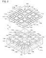
- FIG. 2 is an exploded perspective view showing a state where part of the mechanical quantity sensor 100 (the first structure 110 and the second structure 130) is further disassembled.
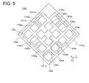
- FIG. 3, FIG. 4 , and FIG. 5 are top views of the first structure 110, the joining part 120, and the second structure 130 respectively.
- FIG. 6, FIG. 7 , and FIG. 8 are a bottom view of the first base 140, a top view of the second base 150, and a bottom view of the second base 150 respectively.
- FIG. 9 and FIG. 10 are cross-sectional views of the mechanical quantity sensor 100 taken along B-B and C-C in FIG. 1 respectively.
- the mechanical quantity sensor 100 in a stand-alone state or in combination with a circuit board (for example, mounted on a board) functions as an electronic component.
- the mechanical quantity sensor 100 as the electronic component is mountable on a game machine, a mobile terminal (for example, a mobile phone), and the like.
- the mechanical quantity sensor 100 and the circuit board (active elements such as IC and wiring terminals on the circuit board) are electrically connected by wire bonding, flip-chipping, or the like.
- the mechanical quantity sensor 100 is capable of measuring one of or both of an acceleration ⁇ and an angular velocity ⁇ . That is, a mechanical quantity means one of or both of the acceleration ⁇ and the angular velocity ⁇ .
- the measurement of accelerations ⁇ x, ⁇ y, ⁇ z is enabled by detecting displacements of a displaceable portion 112 (to be described later) caused by forces FOx, FOy, FOz in X-, Y-, and Z-axis directions.
- the measurement of angular velocities ⁇ x, ⁇ y in the X- and Y-axis directions is enabled by detecting displacements of the displaceable portion 112 caused by Coriolis forces Fy, Fx in the Y- and X-axis directions when the displaceable portion 112 is vibrated in the Z-axis direction.
- the mechanical quantity sensor 100 is capable of measuring the three-axial accelerations ⁇ x, ⁇ y, ⁇ z and the two-axial angular velocities ⁇ x, ⁇ y. This will be described in detail later.
- the first structure 110, the joining part 120, the second structure 130, the first base 140, and the second base 150 each have a substantially square outer periphery having sides each with a 5mm length, for instance, and they have heights of, for example, 20 ⁇ m, 2 ⁇ m, 675 ⁇ m, 500 ⁇ m, and 500 ⁇ m respectively.
- the first structure 110, the joining part 120, and the second structure 130 can be made of silicon, silicon oxide, and silicon respectively, and the mechanical quantity sensor 100 can be manufactured by using a SOI (Silicon On Insulator) substrate having a three-layer structure of silicon/silicon oxide/silicon.
- SOI Silicon On Insulator
- silicon forming the first structure 110 and the second structure 130 it is preferable to use a conductive material which as a whole contains impurities such as boron.
- impurity-containing silicon for forming the first structure 110 and the second structure 130 can simplify wiring of the mechanical quantity sensor 100.
- impurity-containing silicon is used for the first structure 110 and the second structure 130.
- first base 140 and the second base 150 each can be made of a glass material.
- the first structure 110 has a substantially square outer shape and includes a fixed portion 111(111a to 111c), the displaceable portion 112 (112a to 112e), a connection portion 113 (113a to 113d), and a block upper layer portion 114 (114a to 114j).
- the first structure 110 can be fabricated in such a manner that openings 114a to 114d and the block upper layer portions 114a to 114j are formed by etching a film of a semiconductor material.
- the fixed portion 111 can be divided into the frame portion 111a and the projecting portions 111b, 111c.
- the frame portion 111a is a frame-shaped substrate whose outer periphery and inner periphery are both in a substantially square shape.
- the projecting portion 111b is disposed in a corner portion of the inner periphery of the frame portion 111a and is a substantially square substrate projecting toward the displaceable portion 112b (in an X direction of an X-Y plane), and the projecting portion 111c is disposed in a corner portion of the inner periphery of the frame portion 111a and is a substantially square substrate projecting toward the displaceable portion 112d (in a 180° direction when the X direction of the X-Y plane is defined as 0°).
- the frame portion 111a and the projecting portions 111b, 111c are integrally formed.
- the displaceable portion 112 is made up of the displaceable portions 112a to 112e.
- the displaceable portion 112a is a substrate having a substantially square outer periphery and is disposed near a center of the opening of the fixed portion 111.
- the displaceable portions 112b to 112e each are a substrate having a substantially square outer periphery and are connected to and surround the displaceable portion 112a from four directions (an X-axis positive direction, an X-axis negative direction, a Y-axis positive direction, and a Y-axis negative direction).
- the displaceable portions 112a to 112e are joined to later-described weight portions 132a to 132e via the joining part 120 respectively and displace as a unit relative to the fixed portion 111.
- An upper surface of the displaceable portion 112a functions as a driving electrode E1 (to be described later).
- the driving electrode E1 being the upper surface of the displaceable portion 112a is capacitively coupled to a later-described driving electrode 144a provided on a lower surface of the first base 140 and by a voltage applied therebetween, the displaceable portion 112 is vibrated in the Z-axis direction. This drivingwill be described in detail later.
- Each of upper surfaces of the displaceable portions 112b to 112e functions as a detection electrode E1 (to be described later) detecting the displacements in the X-axis and Y-axis directions of the displaceable portion 112.
- the detection electrodes being the upper surfaces of the displaceable portions 112b to 112e are capacitively coupled to later-described detection electrodes 144b to 14 4e provided on the lower surf ace of the first base 140 respectively (the alphabets b to e of the displaceable portions 112 correspond to the alphabets b to e of the detection electrodes 144 in order respectively). This detection will be described in detail later.
- connection portions 113a to 113d are substantially rectangular substrates and connect the fixed portion 111 and the displaceable portion 112a in four directions (directions of 45°, 135°, 225°, and 315° when the X direction of the X-Y plane is defined as 0°).
- connection portions 113a to 113d, near the frame portion 111a are joined to projecting portions 131c (to be described later) of a pedestal 131 via the joining part 120.
- projecting portions 131c there are other areas of the connection portions 113a to 113d, that is, in areas near the displaceable portion 112a, no projecting portion 131c is formed in corresponding areas, and these areas have a small thickness and thus have flexibility.
- the reason why the areas, of the connection portions 113a to 113d, near the frame portion 111a is joined to the projecting portions 131c is to prevent the connection portions 113a to 113d from being damaged due to large bending.
- connection portions 113a to 113d function as bendable beams. Since the connection portions 113a to 113d bend, the displaceable portion 112 is displaceable relative to the fixed portion 111. Concretely, the displaceable portion 112 linearly displaces in the Z positive direction and the Z negative direction relative to the fixed portion 111. Further, the displaceable portion 112 is capable of positive and negative rotations with the X axis and the Y axis as rotation axes, relative to the fixed portion 111. That is, the "displacement” here can include the movement and the rotation (the movement in the Z-axis direction and the rotations around the X and Y axes).
- the block upper layer portion 114 is made up of block upper layer portions 114a to 114j.
- the block upper layer portions 114a to 114j are substantially square substrates and are arranged along an inner periphery of the fixed portion 111 to surround the periphery of the displaceable portion 112.
- the block upper layer portions 114h, 114a have end surfaces facing end surfaces of the displaceable portion 112e
- the block upper layer portions 114b, 114c have end surfaces facing end surfaces of the displaceable portion 112b
- the block upper layer portions 114d, 114e have end surfaces facing end surfaces of the displaceable portion 112c
- the block upper layer portions 114f, 114g have end surfaces facing end surfaces of the displaceable portion 112d.
- the block upper layer portions 114a to 114h each have the end surface facing one of the eight end surfaces of the displaceable portion 112 and are arranged clockwise in alphabetical order.
- the block upper layer portion 114i and the block upper layer portion 114j are arranged in directions of 90° and 270° respectively when the X direction of the X-Y plane is defined as 0°.
- the block upper layer portions 114a to 114h are joined to later-described block lower layer portions 134a to 134h respectively via the joining part 120 (the alphabets a to h of the block upper layer portion 114 correspond to the alphabets a to h of the block lower layer portion 134 in order respectively.
- Blocks made by joining the block upper layer portions 114a to 114h and the block lower layer portions 134a to 134h respectively are used as wirings for supplying power to later-described detection electrodes 144b to 144e, 154b to 154e.
- the block upper layer portions 114i, 114j are joined to later-described block lower layer portions 134i, 134j via the joining part 120. Blocks made by joining the block upper layer portions 114i, 114j and the block lower layer portions 134i, 134j respectively are used as wirings for vibrating the displaceable portion 112 in the Z-axis direction. This will be described in detail later.
- the second structure 130 has a substantially square outer shape and includes the pedestal 131 (131a to 131d), the weight portion 132 (132a to 132e), and the block lower layer portion 134 (134a to 134j).
- the second structure 130 can be fabricated in such a manner that an opening 133, the block lower layer portions 134a to 134j, and a pocket 135 (to be described later) are formed by etching a substrate of a semiconductor material.
- the pedestal 131 and the block lower layer portions 134a to 134j are substantially equal in height, and the weight portion 132 is lower in height than the pedestal 131 and the block lower layer portions 134a to 134j.
- the pedestal 131, the block lower layer portions 134a to 134j, and the weight portion 132 are disposed to be apart from one another.
- the pedestal 131 can be divided into the frame portion 131a and the projecting portions 131b to 131d.
- the frame portion 131a is a frame-shaped substrate whose outer periphery and inner periphery are both in a substantially square shape and has a shape corresponding to the frame portion 111a of the fixed portion 111.
- the projecting portion 131b is disposed in a corner portion of the inner periphery of the frame portion 131a and is a substantially square substrate projecting toward the weight portion 132b (in a 0° direction when the X direction of the X-Y plane is defined as 0°) and has a shape corresponding to the projecting portion 111b of the fixed portion 111.
- the projecting portions 131c are four substantially rectangular substrates, which project from the frame portion 131a toward the weight portion 132a in directions of 45°, 135°, 225°, and 315° respectively when the X direction of the X-Y plane is defined as 0°), and have one-side ends connected to the frame portion 131a of the pedestal 131 and the other ends apart from the weight portion 132a.
- the projecting portions 131c are formed in substantially half areas on the frame portion 131a side, in areas corresponding to the connection portions 113a to 113d, and are not formed in the other areas, that is, in substantially half areas on the weight portion 132 side.
- the projecting portion 131d is disposed in a corner portion of the inner periphery of the frame portion 131a, and is a substantially square substrate projecting toward the weight portion 132d (in a 180° direction when the X direction of the X-Y plane is defined as 0°), with the pocket 135 (opening) being formed so as to pass through a front surface and a rear surface of the substrate, and is joined to the projecting portion 111c of the fixed portion 111.
- the pocket 135 is, for example, a rectangular parallelepiped space where a getter material for maintaining high vacuum is disposed.
- One opening end of the pocket 135 is covered by the joining part 120.
- the other opening end of the pocket 135 is mostly covered by the second base 150, but part thereof near the weight portion 132 is not covered, and this other opening end and the opening 133 where the weight portion 132 and so on are formed partly communicate with each other (not shown).
- the getter material adsorbs residual gas in order to enhance the degree of vacuum in the vacuum-sealed mechanical quantity sensor 100. This can reduce an influence by air resistance when the displaceable portion 112 (the weight portion 132 as well) vibrates.
- the getter material used in the mechanical quantity sensor 100 usable is, for example, a mixture of titanium and a Zr-V-Fe alloy (manufactured by SAES Getters Japan, product name: Non-evaporable Getter St122, activatable in a temperature range of 300 to 500°C).
- the activationof the gettermaterial means that molecules (including gas molecules to be adsorbed) adhering to a surface of the getter material diffuse inside and a new surface having a gas adsorbing power is produced.
- the activation temperature means a temperature at which the new surface having such a gas molecule adsorbing power is produced.
- the frame portion 131a and the projecting portions 131b to 131d are integrally formed.
- the pedestal 131 is connected to the fixed portion 111 and predetermined areas of the connection portions 113a to 113d via the joining part 120.
- the weight portion 132 functions as a heavy weight or an operated body having a mass and receiving the force FO and the Coriolis force F caused by the acceleration ⁇ and the angular velocity w respectively. That is, when the acceleration ⁇ and the angular velocity ⁇ are applied, the force FO and the Coriolis force F act on the center of gravity of the weight portion 132.
- the weight portion 132 is divided into the weight portions 132a to 132e in a substantially rectangular parallelepiped shape.
- the weight portions 132b to 132e are connected to the center weight portion 132a from the four directions and are displaceable (movable, rotatable) as a unit. That is, the weight portion 132a functions as a connection portion connecting the weight portions 132b to 132e.
- the weight portions 132a to 132e each have a substantially square cross section corresponding to those of the displaceable portions 112a to 112e and are joined to the displaceable portions 112a to 112e via the joining part 120.
- the displaceable portion 112 displaces according to the force FO and the Coriolis force F applied to the weight portion 132 and as a result, the acceleration ⁇ and the angular velocity ⁇ can be measured.
- the reason why the weight portion 132 is composed of the weight portions 132a to 132e is to realize both the downsizing and improved sensitivity of the mechanical quantity sensor 100.
- Downsizing the mechanical quantity sensor 100 results in a reduction in capacity of the weight portion 132 and a reduction in its mass, leading to deteriorated sensitivity to the angular velocity.
- the weight portion 132 can have a sufficient mass. As a result, the downsizing and improved sensitivity of the mechanical quantity sensor 100 can be both realized.
- a rear surface of the weight portion 132a functions as a driving electrode E1 (to be described later).
- the driving electrode E1 being the rear surface of the weight portion 132a is capacitively coupled to a later-described driving electrode 154a provided on an upper surface of the second base 150, and by a voltage applied therebetween, the displaceable portion 112 is vibrated in the Z-axis direction. This driving will be described in detail later.
- Rear surfaces of the weight portions 132b to 132e function as detection electrodes E1 (to be described later) detecting the displacements of the displaceable portion 112 in the X-axis and Y-axis directions.
- the detection electrodes E1 being the rear surfaces of the weight portions 132b to 132e are capacitively coupled to later-described detection electrodes 154b to 154e provided on the upper surface of the second base 150 respectively (the alphabets b to e of the weight portion 132 correspond to the alphabets b to e of the detection electrode 154 in order respectively). This detection will be described in detail later.
- the block lower layer portions 134a to 134j have substantially square cross sections corresponding to those of the block upper layer portions 114a to 114j respectively and are joined to the block upper layer portions 114a to 114j via the joining part 120.
- the blocks made by joining the block upper layer portions 114a to 114h and the block lower layer portions 134a to 134h will be hereinafter referred to as "blocks a to h" respectively.
- the blocks a to h are used as the wirings for supplying power to the detection electrodes 144b to 144e, 154b to 154e respectively.
- blocks i, j The blocks made by joining the block upper layer portions 114i, 114j and the block lower layer portions 134i, 134j (hereinafter, referred to as "blocks i, j" respectively) are used as the wirings for vibrating the displaceable portion 112 in the Z-axis direction. This will be described in detail later.
- the joining part 120 connects the first and second structures 110, 130 as previously described.
- the joining part 120 is divided into a joining part 121 connecting the predetermined areas of the connection portion 113 and the fixed portion 111 to the pedestal 131, a joining part 122 (122a to 122e) connecting the displaceable portions 112a to 112e to the weight portions 132a to 133e, and a joining part 123 (123a to 123j) connecting the block upper layer portions 114a to 114j to the block lower layer portions 134a to 134j.
- the joining part 120 does not connect the other portions of the first and second structures 110, 130. This is intended to allow the connection portions 113a to 113d to bend and allow the weight portion 132 to displace. It is possible to form the joining parts 121, 122, 123 by etching a silicon oxide film.
- Conduction portions 160 to 162 are formed in order to bring the first structure 110 and the second structure 130 into electrical continuity at necessary portions.
- the conduction portion 160 brings the fixed portion 111 and the pedestal 131 into electrical continuity and passes through the projecting portion 111b of the fixed portion 111 and the joining part 121.
- the conduction portion 161 brings the displaceable portion 112 and the weight portion 132 into electrical continuity and passes through the displaceable portion 112a and the joining part 122.
- the conduction portions 162 bring the block upper layer portions 114a, 114b, 114e, 114f, 114i and the block lower layer portions 134a, 134b, 134e, 134f, 134i into electrical continuity respectively and pass through the block upper layer portions 114a, 114b, 114e, 114f, 114i and the joining part 123 respectively.
- the conduction portions 160 to 162 are each made up of a through hole and a layer of metal such as, for example, Al formed on an edge, a wall surface, and a bottom of the through hole.
- the shape of the through holes is not specifically limited, but the through holes of the conduction portions 160 to 162 are preferably in a conical shape fanning out upward since the metal layers can be effectively formed on the through holes in such a shape by sputtering or the like of Al or the like.
- the first base 140 is made of, for example, a glass material, has a substantially rectangular parallelepiped outer shape, and has a frame portion 141 and a bottom plate portion 142. It is possible to fabricate the frame portion 141 and the bottom plate portion 142 by forming a substantially rectangular parallelepiped recessed portion 143 (for example, 2.5 mm square and 5 ⁇ m depth) in a substrate.
- the frame portion 141 is a frame-shaped substrate whose outer periphery and inner periphery are both substantially square.
- the outer periphery of the frame portion 141 matches the outer periphery of the fixed portion 111, and the inner periphery of the frame portion 141 is smaller than the inner periphery of the fixed portion 111.
- the bottom plate portion 142 has a substrate shape whose outer periphery is in a substantially square shape which is the same as that of the frame portion 141.
- the reason why the recessed portion 143 is formed in the first base 140 is to reserve a space where the displaceable portion 112 displaces.
- the first structure 110 except the displaceable portion 112, that is, the fixed portion 111 and the block upper layer portions 114a to 114j are joined to the first base 140 by, for example, anodic bonding.
- the driving electrode 144a and the detection electrodes 144b to 144e are disposed on the bottom plate portion 142 (on a rear surface of the first base 140) so as to face the displaceable portion 112.
- the driving electrode 144a and the detection electrodes 144b to 144e can all be made of a conductive material.
- the driving electrode 144a is, for example, in a cross shape and is formed near the center of the recessed portion 143 so as to face the displaceable portion 112a.
- the detection electrodes 144b to 144e are each in a substantially square shape, surround the driving electrode 144a from the four directions (the X-axis positive direction, the X-axis negative direction, the Y-axis positive direction, and the Y-axis negative direction), and are disposed to face the displaceable portions 112b to 112e in order respectively.
- the driving electrode 144a and the detection electrodes 144b to 144e are apart from one another.
- a wiring layer L1 electrically connected to an upper surface of the block upper layer portion 114i is connected to the driving electrode 144a.
- a wiring layer L4 electrically connected to an upper surface of the block upper layer portion 114b is connected to the detection electrode 144b
- a wiring layer L5 electrically connected to an upper surface of the block upper layer portion 114e is connected to the detection electrode 144c
- a wiring layer L6 electrically connected to an upper surface of the block upper layer portion 114f is connected to the detection electrode 144d
- a wiring layer L7 electrically connected to an upper surface of the block upper layer portion 114a is connected to the detection electrode 144e.
- the driving electrode 144a As a material forming the driving electrode 144a, the detection electrodes 144b to 144e, and the wiring layers L1, L4 to L7, Nd-containing Al is usable, for instance.
- Nd-containing Al for the driving electrode 144a, the detection electrodes 144b to 144e, and so on makes it possible to prevent hillocks from being generated in the driving electrode 144a, the detection electrodes 144b to 144e, and so on during later-described heat treatment processes (the anodic bonding of the first base 140 or the second base 150, the activation of the getter material).
- the hillocks here are, for example, semispherical protuberances.
- dimension precision of a distance between the driving electrode 144a and the driving electrode E1 (capacitively coupled to the driving electrode 144a) formed on the upper surface of the displaceable portion 112a and distances between the detection electrodes 144b to 144e and the detection electrodes E1 (capacitively coupled to the detection electrodes 144b to 144e in order respectively) formed on the upper surfaces of the displaceable portions 112b to 122e respectively can be enhanced.
- the dimension precision between the driving electrodes 144a and E1 and between the detection electrodes 144b to 144e and E1 can be thus enhanced, which as a result can reduce variation in capacitance value and reduce variation in characteristic among products.
- Nd-containing Al as the material forming the wiring layers L1, L4 to L7 makes it possible to firmly join the first base 140 and the first structure 110. End portions of the wiring layers L1, L4 to L7 (end portions on a side not joined to the driving electrode 144a and the detection electrodes 144b to 144e) are sandwiched between the lower surface of the first base 140 and the upper surfaces of the block upper layer portions 114i, 114b, 114e, 114f, 114a in order respectively.
- Nd-containing Al is relatively flexible and thus is easily crushed flat. Therefore, at the time of the anodic bonding of the first base 140 and the first structure 110, the end portions of the wiring layers L1, L4 to L7 are easily crushed flat and do not obstruct the anodic bonding.
- the driving electrode 144a, the detection electrodes 144b to 144e, and the wiring layers L1, L4 to L7 can be formed simultaneously by single patterning, which can simplify manufacturing processes.
- the second base 150 is made of, for example, a glass material and has a substantially square substrate shape. Portions of the second structure 130 excluding the weight portion 132, that is, the pedestal 131 and the block lower layer portions 134a to 134j, are joined to the second base 150 by, for example, anodic bonding. The weight portion 132 is lower in height than the pedestal 131 and the block lower layer portions 134a to 134j and thus is not joined to the second base 150. This is intended to reserve a gap between the weight portion 132 and the second base 150 and allow the weight portion 132 to displace.
- the driving electrode 154a and the detection electrodes 154b to 154e are disposed so as to face the weight portion 132.
- the driving electrode 154a and the detection electrodes 154b to 154e can all be made of a conductive material.
- the driving electrode 154a is in, for example, a cross shape and is formed near the center of the upper surface of the second base 150 so as to face the weight portion 132a.
- the detection electrodes 154b to 154e are each in a substantially square shape, surround the driving electrode 154a from the four directions (the X-axis positive direction, the X-axisnegative direction, the Y-axis positive direction, and the Y-axis negative direction), and are disposed to face the weight portions 132b to 132e respectively.
- the driving electrode 154a and the detection electrodes 154b to 154e are apart from one another.
- a wiring layer L2 electrically connected to a rear surface of the block lower layer portion 134j is connected to the driving electrode 154a.
- a wiring layer L8 electrically connected to a rear surface of the block lower layer portion 134c is connected to the detection electrode 154b
- a wiring layer L9 electrically connected to a rear surface of the block lower layer portion 134d is connected to the detection electrode 154c
- a wiring layer L10 electrically connected to a rear surface of the block lower layer portion 134g is connected to the detection electrode 154d
- a wiring layer L11 electrically connected to a rear surface of the block lower layer portion 134h is connected to the detection electrode 154e.
- the driving electrode 154a As a material forming the driving electrode 154a, the detection electrodes 154b to 154e, and the wiring layers L2, L8 to L11, Nd-containing Al is usable, for instance.
- Nd-containing Al for the driving electrode 154a and the detection electrodes 154b to 154e makes it possible to prevent hillocks from being generated in the driving electrode 154a, the detection electrodes 154b to 154e, and so on during later-described heat treatment processes (the anodic bonding of the second base 150, the activation of the getter material).
- dimension precision of a distance between the driving electrode 154a and the driving electrode E1 (capacitively coupled to the driving electrode 154a) formed on the lower surface of the weight portion 132a and distances between the detection electrodes 154b to 154e and the detection electrodes E1 (capacitively coupled to the detection electrodes 154b to 154e in order respectively) formed on the upper surfaces of the weight portions 132b to 132e respectively can be enhanced.
- the dimension precision between the driving electrodes 154a and E1 and between the detection electrodes 154b to 154e and E1 can be thus enhanced, which as a result can reduce variation in capacitance value and reduce variation in characteristic among products.
- Nd-containing Al as the material forming the wiring layers L2, L8 to L11 makes it possible to firmly join the second base 150 and the second structure 130. End portions of the wiring layers L2, L8 to L11 (end portions on a side not joined to the driving electrode 154a and the detection electrodes 154b to 154e) are sandwiched between the upper surface of the second base 150 and lower surfaces of the block upper layer portions 134j, 134c, 134d, 134g, 134h in order respectively.
- Nd-containing Al is relatively flexible and thus is easily crushed flat. Therefore, at the time of the anodic bonding of the second base 150 and the second structure 130, the end portions of the wiring layers L2, L8 to L11 are easily crushed flat and thus do not obstruct the anodic bonding.
- the driving electrode 154a, the detection electrodes 154b to 154e, and the wiring layers L2, L8 to L11 can be formed simultaneously by single patterning, which can simplify manufacturing processes.
- a wiring terminal T (T1 to T11) passing through the second base 150 is provided in the second base 150 enable electrical connection to the driving electrodes 144a, 154a, the detection electrodes 144b to 144e, 154b to 154e from an external part of the mechanical quantity sensor 100.
- An upper end of the wiring terminal T1 is connected to a rear surface of the projecting portion 131b of the pedestal 131.
- the wiring terminals T2 to T9 are connected to rear surfaces of the block lower layer portions 134a to 134h respectively (the numerical order of T2 to T9 of the wiring terminals T2 to T9 corresponds to the alphabetical order of 134a to 134h of the block lower layer portions 134a to 134h respectively).
- the wiring terminals T10, T11 are connected to rear surfaces of the block lower layer portions 134i, 134j respectively.
- the wiring terminal T is made up of, for example, a conical through hole fanning out upward and a film of metal such as, for example, Al formed on an edge, a wall surface, and a bottom of the conical through hole, and has the same structure as that of the conduction portions 160 to 162.
- the wiring terminal T is usable as a connection terminal which is connected to an external circuit by, for example, wire bonding.
- the second base 150 is shown on a lower side in consideration of easier view of the first structure 110, the joining part 120, and the second structure 130.
- the wiring terminal T and the external circuit are connected by, for example, wire bonding
- setting the second base 150 of the mechanical quantity sensor 100 on an upper side can facilitate the connection.
- the wiring and electrodes of the mechanical quantity sensor 100 will be described.
- FIG. 11 is a cross-sectional view showing six pairs of capacitor elements in the mechanical quantity sensor 100 shown in FIG. 9 .
- portions functioning as electrodes are hatched.
- FIG. 11 shows the six pairs of capacitor elements, the ten pairs of capacitor elements are formed in the mechanical quantity sensor 100 as previously described.
- Electrodes as one-side mates of the ten pairs of capacitor elements are the driving electrode 144a and the detection electrodes 144b to 144e, which are formed on the first base 140, and the driving electrode 154a and the detection electrodes 154b to 154e, which are formed on the second base 150.
- the other mates of the ten pairs of capacitor elements are the driving electrode E1 being the upper surface of the displaceable portion 112a, the detection electrodes E1 formed on the upper surfaces of the displaceable portions 112b to 112e respectively, the driving electrode E1 being the lower surface of the weight portion 132a, and the detection electrodes E1 formed on the lower surfaces of the weight portions 132b to 132e respectively. That is, the block made by joining the displaceable portion 112 and the weight portion 132 functions as a common electrode of the ten pairs of capacitive couplings. Since the first structure 110 and the second structure 130 are made of the conductive material (impurity-containing silicon), the block made by joining the displaceable portion 112 and the weight portion 132 can function as an electrode.
- the capacitance of a capacitor is inversely proportional to the distance between its electrodes, and therefore it is assumed that the driving electrodes E1 and the detection electrodes E1 are on the upper surface of the displaceable portion 112 and the lower surface of the weight portion 132. That is, the driving electrodes E1 and the detection electrodes E1 are not formed as separate bodies on outer layers of the upper surface of the displaceable portion 112 and the lower surface of the weight portion 132. It is understood that the upper surface of the displaceable portion 112 and the lower surface of the weight portion 132 function as the driving electrodes E1 and the detection electrodes E1.
- the driving electrode 144a and the detection electrodes 144b to 144e formed on the first base 140 are electrically connected to the block upper layer portions 114i, 114b, 114e, 114f, 114a via the wiring layers L1, L4 to L7 in order respectively. Further, the block upper layer portions 114i, 114b, 114e, 114f, 114a and the block lower layer portions 134i, 134b, 134e, 134f, 134a are in electrical continuity with each other respectively via the conduction portion 162.
- the driving electrode 154a and the detection electrodes 154b to 154e formed on the second base 150 are electrically connected to the block lower layer portions 134j, 134c, 134d, 134g, 134h via the wiring layers L2, L8 to L11 in order respectively.
- wirings for these driving electrodes 144a, 154a and detection electrodes 144b to 144e, 154b to 154e only have to be connected to the lower surfaces of the block lower layer portions 134a to 134j.
- the wiring terminals T2 to T9 are disposed on the lower surfaces of the block lower layer portions 134a to 134h respectively, and the wiring terminals T10, T11 are disposed on the lower surfaces of the block lower layer portions 134i, 134j respectively.
- the wiring terminals T2 to T11 are electrically connected to the detection electrodes 144e, 144b, 154b, 154c, 144c, 144d, 154d, 154e and the driving electrodes 144a, 154a in order respectively.
- the driving electrodes E1 and the detection electrodes E1 are formed by the upper surface of the displaceable portion 112 and the lower surface of the weight portion 132.
- the displaceable portion 112 and the weight portion 132 are in electrical continuity via the conduction portion 161 and are both made of the conductive material.
- the pedestal 131 and the fixed portion 111 are in electrical continuity via the conduction portion 160 and are both made of the conductive material.
- the displaceable portion 112, the connection portion 113, and the fixed portion 111 are integrally formed of the conductive material. Therefore, wirings for the driving electrodes E1 and the detection electrodes E1 only have to be connected to the lower surface of the pedestal 131.
- the wiring terminal T1 is disposed on the lower surface of the projecting portion 131b of the pedestal 131, and the wiring terminal T1 is electrically connected to the driving electrodes E1 and the detection electrodes E1.
- the blocks a to j made by joining the block upper layer portions 114a to 114j and the block lower layer portions 134a to 134j can have the function as the wirings, which can simplify the wirings to the capacitor elements.
- the alternate voltage application between the driving electrodes 144a and E1 and between the driving electrodes 154a and E1 causes the displaceable portion 112 (the weight portion 132 as well) to vibrate in the Z-axis direction.
- a positive or negative DC waveform (a pulse waveform considering the non-application time), a half-wave waveform, or the like is usable.
- the driving electrodes 144a and E1 (the upper surface of the displaceable portion 112a), and the driving electrodes 154a and E1 (the lower surf ace of the weight portion 132a) function as vibration appliers, and the detection electrodes 144b to 144e, 154b to 154e and E1 (the upper surfaces of the displaceable portions 112b to 112e and the lower surfaces of the weight portions 132b to 132e) function as displacement detectors.
- a period of the vibration of the displaceable portion 112 is determined by a cycle at which the voltages are switched. This switching cycle is preferably close to some degree to a natural frequency of the displaceable portion 112.
- the natural frequency of the displaceable portion 112 is determined by elasticity of the connection portion 113, the mass of the weight portion 132, and the like. If the period of the vibration applied to the displaceable portion 112 does not correspond to the natural frequency, energy of the vibration applied to the displaceable portion 112 is diverged, resulting in lower energy efficiency.
- an AC voltage with a 1/2 frequency of the natural frequency of the displaceable portion 112 may be applied either between the driving electrodes 144a and E1 or between the driving electrodes 154a and E1.
- the displacement (inclination) of the displaceable portion 112 is caused by the acceleration ⁇ and the angular velocity ⁇ .
- the displacement of the displaceable portion 112 can be detected based on the detection electrodes 144b to 144e, 154b to 154e.
- the capacitance between the detection electrodes E1 (the upper surface of the displaceable portion 112c) and 114c and the capacitance between the detection electrodes E1 (the upper surface of the displaceable portion 112e) and 144e both increase.
- the distance between the driving electrodes E1 (the upper surface of the displaceable portion 112c) and 144c and the distance between the detection electrodes E1 (the lower surface of the weight portion 132e) and 154e decrease, and the distance between the detection electrodes E1 (the upper surface of the displaceable portion 112e) and 144e and the distance between the detection electrodes E1 (the lower surface of the weight portion 132c) and 154c increase.
- the capacitance between the detection electrodes E1 (the upper surface of the displaceable portion 112c) and 144c and the capacitance between the detection electrodes E1 (the lower surface of the weight portion 132e) and 154e increase, and the capacitance between the detection electrodes E1 (the upper surface of the displaceable portion 112e) and 144e and the capacitance between the detection electrodes E1 (the lower surface of the weight portion 132c) and 154c decrease.
- the inclinations in the X direction and the Y direction and the displacement in the Z direction of the displaceable portion 112 are detected based on the detection electrodes E1, 144b to 144e, 145b to 154e.
- the bias components (accelerations) with a lower frequency than the vibration frequency of the displaceable portion 112 and vibration components (angular velocities) with the same frequency as the vibration frequency of the displaceable portion 112 are extracted by frequency analysis of the detection signals.
- the mechanical quantity sensor 100 is capable of measuring the accelerations ⁇ x, ⁇ y, ⁇ z in the X, Y, Z directions (three axes) and the angular velocities ⁇ x, ⁇ y in the X and Y directions (two axes).
- FIG. 12 is a flowchart showing an example of the fabrication procedure of the mechanical quantity sensor 100.
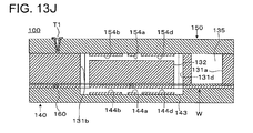
- FIG. 13A to FIG. 13J are cross-sectional views showing states of the mechanical quantity sensor 100 in the fabrication procedure in FIG. 12 (corresponding to a cross section of the mechanical quantity sensor 100 in FIG. 1 taken along C-C).
- FIG. 13A to FIG. 13J correspond to cross-sectional views where the mechanical quantity sensor 100 in FIG. 10 is set upside down.
- Step S10 and FIG. 13A a semiconductor substrate W made up of three stacked layers, that is, first, second, and third layers 11, 12, 13, is prepared.
- the first, second, and third layers 11, 12, 13 are layers for forming the first structure 110, the joining part 120, and the second structure 130 respectively, and here, are layers made of impurity-containing silicon, silicon oxide, and impurity-containing silicon respectively.
- the semiconductor substrate W having a stack structure of the three layers of impurity-containing silicon /silicon oxide/ impurity-containing silicon can be fabricated in such a manner that a substrate made up of an impurity-containing silicon substrate with a silicon oxide film stacked thereon and an impurity-containing silicon substrate are joined and thereafter, the latter impurity-containing silicon substrate is thinly polished (what is called a SOI substrate).
- the impurity-containing silicon substrate can be manufactured by, for example, doping boron in the manufacture of silicon single crystals by a Czochralski method.
- An example of the impurities contained in silicon is boron.
- boron-containing silicon usable is, for example, that containing high-concentration boron and having a 0.001 to 0.01 ⁇ •cm resistivity.
- first layer 11 and the third layer 13 are made of the same material (impurity-containing silicon), but all of the first, second, and third layers 11, 12, 13 may be made of different materials.
- First Structure 110 (Etching of First Layer 11, Step S11, and FIG. 13B )
- the opening 115 is formed and the first structure 110 is formed. That is, by using an etching method erosive to the first layer 11 and not erosive to the second layer 12, predetermined areas (the openings 115a to 115d) of the first layer 11 are etched in a thickness direction until an upper surface of the second layer 12 is exposed.
- a resist layer having a pattern corresponding to the first structure 110 is formed on an upper surface of the first layer 11 and exposed portions not covered by the resist layer are eroded vertically downward. In this etching process, since the second layer 12 is not eroded, only the predetermined areas (the openings 115a to 115d) of the first layer 11 are removed.
- FIG. 13B shows a state where the first structure 110 is formed by the aforesaid etching of the first layer 11.
- the first structure 110 being residual portions of the first layer 11 functions as a resist layer for the second layer 12.
- the etching is applied to the exposed portions of the second layer 12.
- the first condition is to have directivity in the layer direction as well as the thickness direction
- the second condition is to be erosive to a silicon oxide layer but not to be erosive to a silicon layer.
- the first condition is a condition necessary to prevent the silicon oxide layer from remaining in unnecessary portions to inhibit the degree of freedomof the displacement of the weight portion 132.
- the second condition is a condition necessary to prevent the erosion of the silicon first structure 110, which has already been processed to a predetermined shape, and the third layer 13.
- Step S13 and FIG. 13D Formation of Conduction Portions 160 to 162 (Step S13 and FIG. 13D )
- the conduction portions 160 to 162 are formed in the following manners a, b.
- TMAH tetramethylammonium hydroxide
- Al is deposited by a vapor deposition method, a sputtering method, or the like, whereby the conduction portions 160 to 162 are formed.
- Unnecessary portions of the metal layer deposited on the upper surface of the first structure 110 are removed by etching.
- the driving electrode 144a, the detection electrodes 144b to 144e, and the wiring layers L1, L4 to L7 are formed at predetermined positions by a pattern made of, for example, Nd-containing Al.
- the driving electrode 144a, the detection electrodes 144b to 144e, and the wiring layers L1, L4 to L7 can be formed simultaneously by single patterning, which can simplify the manufacturing processes.
- the semiconductor substrate W and the first base 140 are joined by, for example, anodic bonding.
- the first base 140 is anodically bonded. Since the anodic bonding of the first base 140 precedes the formation of the weight portion 132, the connection portions 113a to 113d have no thin area and do not have flexibility, and therefore, even if electrostatic attraction is generated, the displaceable portion 112 is not attracted to the first base 140. This can prevent the first base 140 and the displaceable portion 112 from being joined.
- FIG. 13E shows a state where the semiconductor substrate W and the first base 140 are joined.
- hillocks may possibly be generated in the driving electrode 144a, the detection electrodes 144b to 144e, and the wiring layers L1, L4 to L7 (hereinafter, referred to as the "driving electrode 144a and so on").
- the use of Nd-containing Al for the driving electrode 144a and so on makes it possible to prevent the generation of hillocks in the driving electrode 144a and so on at the time of the anodic bonding of the first base 140. Consequently, it is possible to enhance dimension precision between the driving electrodes 144a and E1 and between the detection electrodes 144b to 144e and E1, which can as a result reduce variation in capacitance value and thus can reduce variation in characteristic among products.
- the driving electrode 144a and the driving electrode E1 since the generation of hillocks in the driving electrode 144a and so on can be prevented, it is possible to prevent the driving electrode 144a and the driving electrode E1, or the detection electrodes 144b to 144e and the detection electrodes E1, which are to be capacitively coupled, from coming into contact with each other via the hillocks to be short-circuited when the displaceable portion 122 (the weight portion 132 as well) is vibrated in the Z-axis direction by the driving electrodes 144a, 154a.
- Nd-containing Al which is relatively flexible and thus is easily crushed flat is used as the material forming the wiring layers L1, L4 to L7, the wiring layers L1, L4 to L7 do not obstruct the anodic bonding, whichmakes it possible to firmly join the first base 140 and the first structure 110.
- the second structure 130 is formed in the following manners a, b.
- the third layer 13 On an upper surface of the third layer 13 excluding the formation areas of the weight portion 132 and its vicinity, a resist layer is formed, and exposed portions not covered by the resist layer (the formation areas of the weight portion 132 and its vicinity) are eroded vertically downward. As a result, the gap 10 for allowing the displacement of the weight portion 132 is formed on top of the formation area of the weight portion.
- the opening 133, the block lower layer portions 134a to 134j, and the pocket 135 are formed by etching the third layer 13 in which the gap 10 is formed, whereby the second structure 130 is formed. That is, by an etching method erosive to the third layer 13 and not erosive to the second layer 12, a predetermined area (the opening 133) of the third layer 13 is etched in the thickness direction.
- FIG. 13G shows a state where the second structure 130 is formed by the aforesaid etching of the third layer 13.
- an etching method as described below needs to be performed in the process of forming the first structure 110 (Step S11) and the process of forming the second structure 130 (Step S15).
- a first condition is to have directivity in the thickness direction of each layer.
- a second condition is to be erosive to a silicon layer and not to be erosive to a silicon oxide layer.
- a possible etching method satisfying the first condition is ICP (Inductively-Coupled Plasma Etching Method).
- This etching method is an effective method to dig a deep groove in the vertical direction and is a kind of an etching method generally called DRIE (Deep Reactive Ion Etching).
- an etching stage where a material layer is continuously dug while being eroded in the thickness direction and a deposition stage where a polymer wall is formed on a side surface of the dug hole are alternately repeated.
- the side surface of the dug hole is protected by the sequentially formed polymer walls, which makes it possible to progress the erosion only in the substantially thickness direction.
- Etching satisfying the second condition is enabled by the use of etching materials having etching selectivity to silicon oxide and silicon.
- a possible example is to use mixed gas of SF 6 gas and O 2 gas in the etching stage and to use C 4 F 8 gas in the deposition stage.
- the driving electrode 154a, the detection electrodes 154b to 154e, and the wiring layers L2, L8 to L11 are formed at predetermined positions by using a pattern made of, for example, Nd-containing Al. Further, by etching the second base 150, eleven pieces of the upwardly fanning-out conical through holes 10 for forming the wiring terminals T1 to T11 are formed at predetermined places. Being made of the same material (Nd-containing Al), the driving electrode 154a, the detection electrodes 154b to 154e, and the wiring layers L2, L8 to L11 can be simultaneously formed by single patterning, which can simplify the manufacturing processes.
- the getter material (manufactured by SAES Getters Japan, product name: Non-evaporable Getter St122) is put in the pocket 135, and the second base 150 and the semiconductor substrate W are joined by, for example, anodic bonding.
- FIG. 13H shows a state where the semiconductor substrate W and the second base 150 are joined.
- hillocks may possibly be generated in the driving electrodes 144a, 154a, the detection electrodes 144b to 144e, 154b to 154e, and the wiring layers L1, L2, L4 to L11 (hereinafter, referred to as the "driving electrodes 144a, 154a and so on").
- the use of Nd-containing Al for the driving electrodes 144a, 154a and so on makes it possible to prevent the generation of hillocks in the driving electrodes 144a, 154a and so on at the time of the anodic bonding of the second base 150.
- Nd-containing Al which is relatively flexibile and thus is easily crushed flat is used as the material forming the wiring layers L2, L8 to L11, the wiring layers L2, L8 to L11 do not obstruct the anodic bonding, which makes it possible to firmly join the second base 150 and the second structure 130.
- Step S17 and FIG. 13I Formation of Wiring Terminals T1 to T11 (Step S17 and FIG. 13I )
- metal layers for example, a Cr layer and an Au layer are formed in this order by a vapor deposition method, a sputtering method, or the like. Unnecessary portions of the metal layers (metal layers outsides edges of upper ends of the wiring terminals T) are removed by etching, whereby the wiring terminals T1 to T11 are formed.
- hillocks may possibly be generated in the driving electrodes 144a, 154a, the detection electrodes 144b to 144e, 154b to 154e, and the wiring layers L1, L2, L4 to L11 (the driving electrodes 144a, 154a and so on).
- the generation of hillocks is prevented by the use of Nd-containing Al for the driving electrodes 144a, 154a and so on.
- the generation of hillocks in the driving electrode 144a, 154a and so on can be prevented as described above, it is possible to prevent the driving electrode 144a and the driving electrode E1, the driving electrode 154a and the driving electrode E1, the detection electrodes 144b to 144e and the detection electrodes E1, or the detection electrodes 154b to 154e and the detection electrodes E1, which are to be capacitively coupled, from coming into contact with each other via the hillocks to be short-circuited.
- the hillocks mentioned here are, for example, semispherical protuberance formed in the driving electrodes 144a, 154a and so on.
- an internal stress of the driving electrodes 144a, 154a and so on changes from a tensile stress to a compressive stress due to a temperature increase by the heating.
- this compressive stress becomes larger than a certain value (a hillock generation stress)
- the plastic deformation of the driving electrodes 144, 154a and so on is started. Due to the compressive stress, constituent atoms of the driving electrodes 144a, 154a and so on move (what is called creep) to gather, so that hillocks are generated.
- the hillock generation stress is temperature-dependent and becomes smaller as the temperature increases. Further, the hillock generation stress is larger than what is called a yield stress. That is, even if the compressive stress exceeds the yield stress, hillocks are not immediately generated.
- the material forming the driving electrodes 144a, 154a and so on is an AlNd alloy
- Nd in the driving electrodes 144a, 154a and so on is re-crystallized to separate out when the temperature increases.
- the structure of the driving electrodes 144a, 154a and so on is reconstructed, so that the internal stress in the driving electrodes 144a, 154a and so on is reduced.
- the generation of hillocks due to the compressive stress is prevented in the driving electrodes 144a, 154a and so on.
- Nd is added to Al, Nd is re-crystallized when the temperature increases, and alleviates the internal stress, so that the generation of hillocks in the driving electrodes 144a, 154a and so on is prevented.
- An amount of Nd added to Al i s preferably 1. 5 to 10at% (atomic percent, atomicity ratio (%)), and more preferably 2 to 3at%.
- the amount of Nd added is small, the internal stress is not sufficiently alleviated, which may possibly cause the generation of hillocks.
- the amount of Nd added is large, internal resistance and hardness of the driving electrodes 144a, 154a and so on become large, which is not preferable.
- an Nd-containing Al film was formed on a glass substrate and the presence/absence of the generation of hillocks due to heat treatment was confirmed.
- the condition for the heat treatment the temperature was set to 400°C and the treatment time was set to one hour. An optical microscope was used to observe the presence/absence of hillocks.
- the getter material for example, manufactured by SAES Getters Japan, product name: Non-evaporable Getter St122
- the driving electrodes 144a, 154a, E1 vibrated the weight portion 132 in the Z direction, it was possible to prevent the driving electrode 144a and the driving electrode E1, the driving electrode 154a and the driving electrode E1, the detection electrodes 144b to 144e and the detection electrodes E1, or the detection electrodes 154b to 154e and the detection electrodes E1, which are to be capacitively coupled, from coming into contact with each other to be short-circuited.
- An embodiment of the present invention is not limited to the above-described embodiment, and this embodiment can be expanded and modified, and the expanded and modified embodiments are included in the technical scope of the present invention.
- the conductive material impurity-containing silicon
- the whole portions thereof are not necessarily made of the conductive material.
- At least necessary portions such as the driving electrodes E1, the detection electrodes E1, a portion bringing the wiring terminal T10 and the upper surface of the block upper layer portion 114i into electrical continuity, and the like may be made of the conductive material.
- these portions are preferably made of, for example, Nd-containing Al since such a material can prevent the generation of hillocks.
- a material such as Al-Ta, Ti, Cr, or Mo is usable, for instance. That is, an alloy such as AlTa is usable for the driving electrodes 144a, 154a and so on.
- Nd prevents the generation of hillocks in the driving electrodes 144a, 154a and so on by alleviating the internal stress when Nd is re-crystallized at the time of the temperature increase.
- a material capable of such alleviation of the internal stress is not limited to Nd.
Landscapes
- Physics & Mathematics (AREA)
- General Physics & Mathematics (AREA)
- Engineering & Computer Science (AREA)
- Radar, Positioning & Navigation (AREA)
- Remote Sensing (AREA)
- Manufacturing & Machinery (AREA)
- Pressure Sensors (AREA)
- Gyroscopes (AREA)
Abstract
Description
- The present invention relates to a mechanical quantity sensor detecting a mechanical quantity, and to a method of manufacturing the same.
- There has been disclosed a technique of an angular velocity sensor detecting an angular velocity, in which a transducer structure made of a semiconductor is joined to a glass substrate (see patent reference 1).
Patent reference 1:JP-A 2002-350138 - However, if driving electrodes which apply stack-direction vibration to a weight portion are made of Al, hillocks (for example, semispherical protuberances) are sometimes generated in the driving electrodes when the transducer structure and the glass substrate are anodically bonded. It has been found out that hillocks, if generated in the driving electrodes, lower dimension precision between the capacitively coupled driving electrodes and thus cause a difference in capacitance value, which may cause variation in characteristic among products. It has been further found out that, if hillocks are generated in the driving electrodes, the two driving electrodes which are to be capacitively coupled come into contact with each other via the hillocks to be short-circuited when the weight portion is vibrated in the stack direction by the driving electrodes.
- Considering the above circumstances, it is an object of the present invention to provide a mechanical quantity sensor realizing a reduction in characteristic variation among products and capable of preventing its driving electrodes which are to be capacitively coupled from coming into contact with each other to be short-circuited, and to provide a method of manufacturing the same.
- A mechanical quantity sensor according to an aspect of the present invention includes: a first structure having a fixed portion with an opening, a displaceable portion disposed in the opening and displaceable relative to the fixed portion, and a connection portion connecting the fixed portion and the displaceable portion to each other, the first structure being made of a first semiconductor material in a flat plate shape; a second structure having a weight portion which is joined to the displaceable portion and a pedestal which surrounds the weight portion and is joined to the fixed portion, the second structure being made of a second semiconductor material and being stacked on the first structure; a first base having a first driving electrode which applies stack-direction vibration to the displaceable portion, is disposed on a surface facing the displaceable portion, and is made of a conductive material containing Al and Nd, the first base being made of an insulating material and being stacked on the first structure while being connected to the fixed portion; and a second base having a second driving electrode which applies stack-direction vibration to the displaceable portion, is disposed on a surface facing the weight portion, and is made of the conductive material, the second base being made of an insulating material and being stacked on the second structure while being connected to the pedestal.
- A method of manufacturing a mechanical quantity sensor according to an aspect of the present invention includes: forming a first structure having a fixed portion with an opening, a displaceable portion disposed in the opening and displaceable relative to the fixed portion, and a connection portion connecting the fixed portion and the displaceable portion to each other, by etching a first layer of a semiconductor substrate in which the first layer made of a first semiconductor material, a second layer made of an insulating material, and a third layer made of a second semiconductor material are stacked in order; stacking, on the first structure, a first base by joining the first base to the fixed portion, the first base having a first driving electrode which applies stack-direction vibration to the displaceable portion, is disposed on a surface facing the displaceable portion, and is made of a conductive material containing Al and Nd, and the first base being made of an insulating material; forming a second structure by etching the third layer, the second structure having a weight portion which is joined to the displaceable portion and a pedestal which surrounds the weight portion and is joined to the fixed portion; and stacking, on the second structure, a second base by joining the second base to the pedestal, the second base having a second driving electrode which applies stack-direction vibration to the displaceable portion, is disposed on a surface facing the weight portion, and is made of the conducive material, and the second base being made of an insulating material, wherein anodic bonding is used in at least one of the stacking the first base on the first structure and the stacking the second base on the second structure.
-
- [
FIG. 1] FIG. 1 is an exploded perspective view showing a state where a mechanical quantity sensor according to a first embodiment of the present invention is disassembled. - [
FIG. 2] FIG. 2 is an exploded perspective view showing the state where the mechanical quantity sensor inFIG. 1 is disassembled. - [
FIG. 3] FIG. 3 is a top view of a first structure. - [
FIG. 4] FIG. 4 is a top view of a joining part. - [
FIG. 5] FIG. 5 is a top view of a second structure. - [
FIG. 6] FIG. 6 is a bottom view of a first base. - [
FIG. 7] FIG. 7 is a top view of a second base. - [
FIG. 8] FIG. 8 is a bottom view of the second base. - [
FIG. 9] FIG. 9 is a cross-sectional view taken along B-B inFIG. 1 . - [
FIG. 10] FIG. 10 is a cross-sectional view taken along C-C inFIG. 1 . - [
FIG. 11] FIG. 11 is a cross-sectional view showing six pairs of capacitor elements in the mechanical quantity sensor shown inFIG. 9 . - [
FIG. 12] FIG. 12 is a flowchart showing an example of the fabrication procedure of the mechanical quantity sensor according to the first embodiment of the present invention. - [
FIG. 13A] FIG. 13A is a cross-sectional view showing a state of the mechanical quantity sensor in the fabrication procedure inFIG. 12 . - [
FIG. 13B] FIG. 13B is a cross-sectional view showing a state of the mechanical quantity sensor in the fabrication procedure inFIG. 12 . - [
FIG. 13C] FIG. 13C is a cross-sectional view showing a state of the mechanical quantity sensor in the fabrication procedure inFIG. 12 . - [
FIG. 13D] FIG. 13D is a cross-sectional view showing a state of the mechanical quantity sensor in the fabrication procedure inFIG. 12 . - [
FIG. 13E] FIG. 13E is a cross-sectional view showing a state of the mechanical quantity sensor in the fabrication procedure inFIG. 12 . - [
FIG. 13F] FIG. 13F is a cross-sectional view showing a state of the mechanical quantity sensor in the fabrication procedure inFIG. 12 . - [
FIG. 13G] FIG.13G is a cross-sectional view showing a state of the mechanical quantity sensor in the fabrication procedure inFIG. 12 . - [
FIG. 13H] FIG. 13H is a cross-sectional view showing a state of the mechanical quantity sensor in the fabrication procedure inFIG. 12 . - [
FIG. 13I] FIG. 13I is a cross-sectional view showing a state of the mechanical quantity sensor in the fabrication procedure inFIG. 12 . - [
FIG. 13J] FIG. 13J is a cross-sectional view showing a state of the mechanical quantity sensor in the fabrication procedure inFIG. 12 . - 100...mechanical quantity sensor, 110... first structure, 111... fixed portion, 111a... frame portion, 111b, 111c...projecting portion, 112 (112a - 112e)... displaceable portion, 113 (113a - 113d)... connection portion, 114 (114a - 114j)... block upper layer portion, 115 (115a - 115d)... opening, 120, 121, 122, 123... joining part, 130... second structure, 131... pedestal, 131a... frame portion, 131b - 131d... projecting portion, 132 (132a-133e)...weightportion, 133...opening, 134 (134a - 134j)... block lower layer portion, 135
... pocket 140... first base, 141... frame portion, 142...bottom plate portion 143... recessed portion, 144a... driving electrode, 144b - 144e... detection electrode, 150... second base, 154a... driving electrode, 154b - 154e... detection electrode, 160 - 162... conduction portion, 10... gap, 11... conical through hole, L1, L2, L4 - L11... wiring layer, T1 - T11... wiring terminal, E1... driving electrode, detection electrode - Hereinafter, an embodiment of the present invention will be described in detail with reference to the drawings.
-
FIG. 1 is an exploded perspective view showing a state where amechanical quantity sensor 100 is disassembled. Themechanical quantity sensor 100 has afirst structure 110, a joiningpart 120, and asecond structure 130 which are stacked on one another, afirst base 140, and asecond base 150.FIG. 2 is an exploded perspective view showing a state where part of the mechanical quantity sensor 100 (thefirst structure 110 and the second structure 130) is further disassembled.FIG. 3, FIG. 4 , andFIG. 5 are top views of thefirst structure 110, the joiningpart 120, and thesecond structure 130 respectively.FIG. 6, FIG. 7 , andFIG. 8 are a bottom view of thefirst base 140, a top view of thesecond base 150, and a bottom view of thesecond base 150 respectively.FIG. 9 andFIG. 10 are cross-sectional views of themechanical quantity sensor 100 taken along B-B and C-C inFIG. 1 respectively. - The
mechanical quantity sensor 100 in a stand-alone state or in combination with a circuit board (for example, mounted on a board) functions as an electronic component. Themechanical quantity sensor 100 as the electronic component is mountable on a game machine, a mobile terminal (for example, a mobile phone), and the like. Themechanical quantity sensor 100 and the circuit board (active elements such as IC and wiring terminals on the circuit board) are electrically connected by wire bonding, flip-chipping, or the like. - The
mechanical quantity sensor 100 is capable of measuring one of or both of an acceleration α and an angular velocity ω. That is, a mechanical quantity means one of or both of the acceleration α and the angular velocity ω. The measurement of accelerations αx, αy, αz is enabled by detecting displacements of a displaceable portion 112 (to be described later) caused by forces FOx, FOy, FOz in X-, Y-, and Z-axis directions. Further, the measurement of angular velocities ωx, ωy in the X- and Y-axis directions is enabled by detecting displacements of the displaceable portion 112 caused by Coriolis forces Fy, Fx in the Y- and X-axis directions when the displaceable portion 112 is vibrated in the Z-axis direction. In this manner, themechanical quantity sensor 100 is capable of measuring the three-axial accelerations αx, αy, αz and the two-axial angular velocities ωx, ωy. This will be described in detail later. - The
first structure 110, the joiningpart 120, thesecond structure 130, thefirst base 140, and thesecond base 150 each have a substantially square outer periphery having sides each with a 5mm length, for instance, and they have heights of, for example, 20 µm, 2 µm, 675 µm, 500 µm, and 500 µm respectively. - The
first structure 110, the joiningpart 120, and thesecond structure 130 can be made of silicon, silicon oxide, and silicon respectively, and themechanical quantity sensor 100 can be manufactured by using a SOI (Silicon On Insulator) substrate having a three-layer structure of silicon/silicon oxide/silicon. As silicon forming thefirst structure 110 and thesecond structure 130, it is preferable to use a conductive material which as a whole contains impurities such as boron. As will be describe later, the use of impurity-containing silicon for forming thefirst structure 110 and thesecond structure 130 can simplify wiring of themechanical quantity sensor 100. In this embodiment, impurity-containing silicon is used for thefirst structure 110 and thesecond structure 130. - Further, the
first base 140 and thesecond base 150 each can be made of a glass material. - The
first structure 110 has a substantially square outer shape and includes a fixed portion 111(111a to 111c), the displaceable portion 112 (112a to 112e), a connection portion 113 (113a to 113d), and a block upper layer portion 114 (114a to 114j). Thefirst structure 110 can be fabricated in such a manner thatopenings 114a to 114d and the blockupper layer portions 114a to 114j are formed by etching a film of a semiconductor material. - The fixed portion 111 can be divided into the
frame portion 111a and the projectingportions frame portion 111a is a frame-shaped substrate whose outer periphery and inner periphery are both in a substantially square shape. The projectingportion 111b is disposed in a corner portion of the inner periphery of theframe portion 111a and is a substantially square substrate projecting toward thedisplaceable portion 112b (in an X direction of an X-Y plane), and the projectingportion 111c is disposed in a corner portion of the inner periphery of theframe portion 111a and is a substantially square substrate projecting toward thedisplaceable portion 112d (in a 180° direction when the X direction of the X-Y plane is defined as 0°). Theframe portion 111a and the projectingportions - The displaceable portion 112 is made up of the
displaceable portions 112a to 112e. Thedisplaceable portion 112a is a substrate having a substantially square outer periphery and is disposed near a center of the opening of the fixed portion 111. Thedisplaceable portions 112b to 112e each are a substrate having a substantially square outer periphery and are connected to and surround thedisplaceable portion 112a from four directions (an X-axis positive direction, an X-axis negative direction, a Y-axis positive direction, and a Y-axis negative direction). Thedisplaceable portions 112a to 112e are joined to later-describedweight portions 132a to 132e via the joiningpart 120 respectively and displace as a unit relative to the fixed portion 111. - An upper surface of the
displaceable portion 112a functions as a driving electrode E1 (to be described later). The driving electrode E1 being the upper surface of thedisplaceable portion 112a is capacitively coupled to a later-describeddriving electrode 144a provided on a lower surface of thefirst base 140 and by a voltage applied therebetween, the displaceable portion 112 is vibrated in the Z-axis direction. This drivingwill be described in detail later. - Each of upper surfaces of the
displaceable portions 112b to 112e functions as a detection electrode E1 (to be described later) detecting the displacements in the X-axis and Y-axis directions of the displaceable portion 112. The detection electrodes being the upper surfaces of thedisplaceable portions 112b to 112e are capacitively coupled to later-describeddetection electrodes 144b to 14 4e provided on the lower surf ace of thefirst base 140 respectively (the alphabets b to e of the displaceable portions 112 correspond to the alphabets b to e of the detection electrodes 144 in order respectively). This detection will be described in detail later. - The
connection portions 113a to 113d are substantially rectangular substrates and connect the fixed portion 111 and thedisplaceable portion 112a in four directions (directions of 45°, 135°, 225°, and 315° when the X direction of the X-Y plane is defined as 0°). - Areas, of the
connection portions 113a to 113d, near theframe portion 111a are joined to projectingportions 131c (to be described later) of apedestal 131 via the joiningpart 120. In other areas of theconnection portions 113a to 113d, that is, in areas near thedisplaceable portion 112a, no projectingportion 131c is formed in corresponding areas, and these areas have a small thickness and thus have flexibility. The reason why the areas, of theconnection portions 113a to 113d, near theframe portion 111a is joined to the projectingportions 131c is to prevent theconnection portions 113a to 113d from being damaged due to large bending. - The
connection portions 113a to 113d function as bendable beams. Since theconnection portions 113a to 113d bend, the displaceable portion 112 is displaceable relative to the fixed portion 111. Concretely, the displaceable portion 112 linearly displaces in the Z positive direction and the Z negative direction relative to the fixed portion 111. Further, the displaceable portion 112 is capable of positive and negative rotations with the X axis and the Y axis as rotation axes, relative to the fixed portion 111. That is, the "displacement" here can include the movement and the rotation (the movement in the Z-axis direction and the rotations around the X and Y axes). - The block upper layer portion 114 is made up of block
upper layer portions 114a to 114j. The blockupper layer portions 114a to 114j are substantially square substrates and are arranged along an inner periphery of the fixed portion 111 to surround the periphery of the displaceable portion 112. - The block
upper layer portions displaceable portion 112e, the blockupper layer portions displaceable portion 112b,the blockupper layer portions displaceable portion 112c, and the blockupper layer portions displaceable portion 112d. As shown inFIG. 1 , the blockupper layer portions 114a to 114h each have the end surface facing one of the eight end surfaces of the displaceable portion 112 and are arranged clockwise in alphabetical order. The blockupper layer portion 114i and the blockupper layer portion 114j are arranged in directions of 90° and 270° respectively when the X direction of the X-Y plane is defined as 0°. - The block
upper layer portions 114a to 114h are joined to later-described blocklower layer portions 134a to 134h respectively via the joining part 120 (the alphabets a to h of the block upper layer portion 114 correspond to the alphabets a to h of the block lower layer portion 134 in order respectively. Blocks made by joining the blockupper layer portions 114a to 114h and the blocklower layer portions 134a to 134h respectively are used as wirings for supplying power to later-describeddetection electrodes 144b to 144e, 154b to 154e. - The block
upper layer portions lower layer portions part 120. Blocks made by joining the blockupper layer portions lower layer portions - The
second structure 130 has a substantially square outer shape and includes the pedestal 131 (131a to 131d), the weight portion 132 (132a to 132e), and the block lower layer portion 134 (134a to 134j). Thesecond structure 130 can be fabricated in such a manner that anopening 133, the blocklower layer portions 134a to 134j, and a pocket 135 (to be described later) are formed by etching a substrate of a semiconductor material. Thepedestal 131 and the blocklower layer portions 134a to 134j are substantially equal in height, and theweight portion 132 is lower in height than thepedestal 131 and the blocklower layer portions 134a to 134j. This is intended to reserve a gap between theweight portion 132 and thesecond base 150 to allow theweight portion 132 to displace. Thepedestal 131, the blocklower layer portions 134a to 134j, and theweight portion 132 are disposed to be apart from one another. - The
pedestal 131 can be divided into theframe portion 131a and the projectingportions 131b to 131d. Theframe portion 131a is a frame-shaped substrate whose outer periphery and inner periphery are both in a substantially square shape and has a shape corresponding to theframe portion 111a of the fixed portion 111. The projectingportion 131b is disposed in a corner portion of the inner periphery of theframe portion 131a and is a substantially square substrate projecting toward theweight portion 132b (in a 0° direction when the X direction of the X-Y plane is defined as 0°) and has a shape corresponding to the projectingportion 111b of the fixed portion 111. - The projecting
portions 131c are four substantially rectangular substrates, which project from theframe portion 131a toward theweight portion 132a in directions of 45°, 135°, 225°, and 315° respectively when the X direction of the X-Y plane is defined as 0°), and have one-side ends connected to theframe portion 131a of thepedestal 131 and the other ends apart from theweight portion 132a. The projectingportions 131c are formed in substantially half areas on theframe portion 131a side, in areas corresponding to theconnection portions 113a to 113d, and are not formed in the other areas, that is, in substantially half areas on theweight portion 132 side. - The projecting
portion 131d is disposed in a corner portion of the inner periphery of theframe portion 131a, and is a substantially square substrate projecting toward theweight portion 132d (in a 180° direction when the X direction of the X-Y plane is defined as 0°), with the pocket 135 (opening) being formed so as to pass through a front surface and a rear surface of the substrate, and is joined to the projectingportion 111c of the fixed portion 111. - The
pocket 135 is, for example, a rectangular parallelepiped space where a getter material for maintaining high vacuum is disposed. One opening end of thepocket 135 is covered by the joiningpart 120. The other opening end of thepocket 135 is mostly covered by thesecond base 150, but part thereof near theweight portion 132 is not covered, and this other opening end and theopening 133 where theweight portion 132 and so on are formed partly communicate with each other (not shown). - The getter material adsorbs residual gas in order to enhance the degree of vacuum in the vacuum-sealed
mechanical quantity sensor 100. This can reduce an influence by air resistance when the displaceable portion 112 (theweight portion 132 as well) vibrates. As the getter material used in themechanical quantity sensor 100, usable is, for example, a mixture of titanium and a Zr-V-Fe alloy (manufactured by SAES Getters Japan, product name: Non-evaporable Getter St122, activatable in a temperature range of 300 to 500°C). - Inthis specification, the activationof the gettermaterial means that molecules (including gas molecules to be adsorbed) adhering to a surface of the getter material diffuse inside and a new surface having a gas adsorbing power is produced. Further, the activation temperature means a temperature at which the new surface having such a gas molecule adsorbing power is produced.
- The
frame portion 131a and the projectingportions 131b to 131d are integrally formed. Thepedestal 131 is connected to the fixed portion 111 and predetermined areas of theconnection portions 113a to 113d via the joiningpart 120. - The
weight portion 132 functions as a heavy weight or an operated body having a mass and receiving the force FO and the Coriolis force F caused by the acceleration α and the angular velocity w respectively. That is, when the acceleration α and the angular velocity ω are applied, the force FO and the Coriolis force F act on the center of gravity of theweight portion 132. - The
weight portion 132 is divided into theweight portions 132a to 132e in a substantially rectangular parallelepiped shape. Theweight portions 132b to 132e are connected to thecenter weight portion 132a from the four directions and are displaceable (movable, rotatable) as a unit. That is, theweight portion 132a functions as a connection portion connecting theweight portions 132b to 132e. - The
weight portions 132a to 132e each have a substantially square cross section corresponding to those of thedisplaceable portions 112a to 112e and are joined to thedisplaceable portions 112a to 112e via the joiningpart 120. The displaceable portion 112 displaces according to the force FO and the Coriolis force F applied to theweight portion 132 and as a result, the acceleration α and the angular velocity ω can be measured. - The reason why the
weight portion 132 is composed of theweight portions 132a to 132e is to realize both the downsizing and improved sensitivity of themechanical quantity sensor 100. Downsizing the mechanical quantity sensor 100 (reducing its capacity) results in a reduction in capacity of theweight portion 132 and a reduction in its mass, leading to deteriorated sensitivity to the angular velocity. By arranging theweight portions 132b to 132e in a distributed manner so as not to inhibit the bending of theconnection portions 113a to 113d, theweight portion 132 can have a sufficient mass. As a result, the downsizing and improved sensitivity of themechanical quantity sensor 100 can be both realized. - A rear surface of the
weight portion 132a functions as a driving electrode E1 (to be described later). The driving electrode E1 being the rear surface of theweight portion 132a is capacitively coupled to a later-describeddriving electrode 154a provided on an upper surface of thesecond base 150, and by a voltage applied therebetween, the displaceable portion 112 is vibrated in the Z-axis direction. This driving will be described in detail later. - Rear surfaces of the
weight portions 132b to 132e function as detection electrodes E1 (to be described later) detecting the displacements of the displaceable portion 112 in the X-axis and Y-axis directions. The detection electrodes E1 being the rear surfaces of theweight portions 132b to 132e are capacitively coupled to later-describeddetection electrodes 154b to 154e provided on the upper surface of thesecond base 150 respectively (the alphabets b to e of theweight portion 132 correspond to the alphabets b to e of the detection electrode 154 in order respectively). This detection will be described in detail later. - The block
lower layer portions 134a to 134j have substantially square cross sections corresponding to those of the blockupper layer portions 114a to 114j respectively and are joined to the blockupper layer portions 114a to 114j via the joiningpart 120. The blocks made by joining the blockupper layer portions 114a to 114h and the blocklower layer portions 134a to 134h will be hereinafter referred to as "blocks a to h" respectively. The blocks a to h are used as the wirings for supplying power to thedetection electrodes 144b to 144e, 154b to 154e respectively. The blocks made by joining the blockupper layer portions lower layer portions - The joining
part 120 connects the first andsecond structures part 120 is divided into a joiningpart 121 connecting the predetermined areas of the connection portion 113 and the fixed portion 111 to thepedestal 131, a joining part 122 (122a to 122e) connecting thedisplaceable portions 112a to 112e to theweight portions 132a to 133e, and a joining part 123 (123a to 123j) connecting the blockupper layer portions 114a to 114j to the blocklower layer portions 134a to 134j. The joiningpart 120 does not connect the other portions of the first andsecond structures connection portions 113a to 113d to bend and allow theweight portion 132 to displace. It is possible to form the joiningparts -
Conduction portions 160 to 162 are formed in order to bring thefirst structure 110 and thesecond structure 130 into electrical continuity at necessary portions. - The
conduction portion 160 brings the fixed portion 111 and thepedestal 131 into electrical continuity and passes through the projectingportion 111b of the fixed portion 111 and the joiningpart 121. - The
conduction portion 161 brings the displaceable portion 112 and theweight portion 132 into electrical continuity and passes through thedisplaceable portion 112a and the joiningpart 122. - The
conduction portions 162 bring the blockupper layer portions lower layer portions upper layer portions part 123 respectively. - For example, the
conduction portions 160 to 162 are each made up of a through hole and a layer of metal such as, for example, Al formed on an edge, a wall surface, and a bottom of the through hole. The shape of the through holes is not specifically limited, but the through holes of theconduction portions 160 to 162 are preferably in a conical shape fanning out upward since the metal layers can be effectively formed on the through holes in such a shape by sputtering or the like of Al or the like. - The
first base 140 is made of, for example, a glass material, has a substantially rectangular parallelepiped outer shape, and has aframe portion 141 and abottom plate portion 142. It is possible to fabricate theframe portion 141 and thebottom plate portion 142 by forming a substantially rectangular parallelepiped recessed portion 143 (for example, 2.5 mm square and 5 µm depth) in a substrate. - The
frame portion 141 is a frame-shaped substrate whose outer periphery and inner periphery are both substantially square. The outer periphery of theframe portion 141 matches the outer periphery of the fixed portion 111, and the inner periphery of theframe portion 141 is smaller than the inner periphery of the fixed portion 111. Thebottom plate portion 142 has a substrate shape whose outer periphery is in a substantially square shape which is the same as that of theframe portion 141. The reason why the recessedportion 143 is formed in thefirst base 140 is to reserve a space where the displaceable portion 112 displaces. Thefirst structure 110 except the displaceable portion 112, that is, the fixed portion 111 and the blockupper layer portions 114a to 114j are joined to thefirst base 140 by, for example, anodic bonding. - The driving
electrode 144a and thedetection electrodes 144b to 144e are disposed on the bottom plate portion 142 (on a rear surface of the first base 140) so as to face the displaceable portion 112. The drivingelectrode 144a and thedetection electrodes 144b to 144e can all be made of a conductive material. The drivingelectrode 144a is, for example, in a cross shape and is formed near the center of the recessedportion 143 so as to face thedisplaceable portion 112a. Thedetection electrodes 144b to 144e are each in a substantially square shape, surround the drivingelectrode 144a from the four directions (the X-axis positive direction, the X-axis negative direction, the Y-axis positive direction, and the Y-axis negative direction), and are disposed to face thedisplaceable portions 112b to 112e in order respectively. The drivingelectrode 144a and thedetection electrodes 144b to 144e are apart from one another. - A wiring layer L1 electrically connected to an upper surface of the block
upper layer portion 114i is connected to the drivingelectrode 144a. A wiring layer L4 electrically connected to an upper surface of the blockupper layer portion 114b is connected to thedetection electrode 144b, a wiring layer L5 electrically connected to an upper surface of the blockupper layer portion 114e is connected to thedetection electrode 144c, a wiring layer L6 electrically connected to an upper surface of the blockupper layer portion 114f is connected to thedetection electrode 144d, and a wiring layer L7 electrically connected to an upper surface of the blockupper layer portion 114a is connected to thedetection electrode 144e. - As a material forming the driving
electrode 144a, thedetection electrodes 144b to 144e, and the wiring layers L1, L4 to L7, Nd-containing Al is usable, for instance. - The use of Nd-containing Al for the driving
electrode 144a, thedetection electrodes 144b to 144e, and so on makes it possible to prevent hillocks from being generated in the drivingelectrode 144a, thedetection electrodes 144b to 144e, and so on during later-described heat treatment processes (the anodic bonding of thefirst base 140 or thesecond base 150, the activation of the getter material). The hillocks here are, for example, semispherical protuberances. Consequently, dimension precision of a distance between the drivingelectrode 144a and the driving electrode E1 (capacitively coupled to the drivingelectrode 144a) formed on the upper surface of thedisplaceable portion 112a and distances between thedetection electrodes 144b to 144e and the detection electrodes E1 (capacitively coupled to thedetection electrodes 144b to 144e in order respectively) formed on the upper surfaces of thedisplaceable portions 112b to 122e respectively can be enhanced. The dimension precision between the drivingelectrodes 144a and E1 and between thedetection electrodes 144b to 144e and E1 can be thus enhanced, which as a result can reduce variation in capacitance value and reduce variation in characteristic among products. - Further, owing to the prevention of the generation of hillocks in the driving
electrode 144a and thedetection electrodes 144b to 144e, it is possible to prevent the drivingelectrode 144a and the driving electrode E1, or thedetection electrodes 144b to 144e and the detection electrodes E1, which are to be capacitively coupled, from coming into contact with each other to be short-circuited. This is because it is possible to prevent the drivingelectrode 144a and the driving electrode E1, or thedetection electrodes 144b to 144e and the detection electrodes E1, which are to be capacitively coupled, from coming into contact with each other via the hillocks when the displaceable portion 112 (theweight portion 132 as well) is vibrated in the Z-axis direction by the drivingelectrodes - Further, the use of Nd-containing Al as the material forming the wiring layers L1, L4 to L7 makes it possible to firmly join the
first base 140 and thefirst structure 110. End portions of the wiring layers L1, L4 to L7 (end portions on a side not joined to the drivingelectrode 144a and thedetection electrodes 144b to 144e) are sandwiched between the lower surface of thefirst base 140 and the upper surfaces of the blockupper layer portions first base 140 and thefirst structure 110, the end portions of the wiring layers L1, L4 to L7 are easily crushed flat and do not obstruct the anodic bonding. - Further, being made of the same material (Nd-containing Al), the driving
electrode 144a, thedetection electrodes 144b to 144e, and the wiring layers L1, L4 to L7 can be formed simultaneously by single patterning, which can simplify manufacturing processes. - The
second base 150 is made of, for example, a glass material and has a substantially square substrate shape. Portions of thesecond structure 130 excluding theweight portion 132, that is, thepedestal 131 and the blocklower layer portions 134a to 134j, are joined to thesecond base 150 by, for example, anodic bonding. Theweight portion 132 is lower in height than thepedestal 131 and the blocklower layer portions 134a to 134j and thus is not joined to thesecond base 150. This is intended to reserve a gap between theweight portion 132 and thesecond base 150 and allow theweight portion 132 to displace. - On the upper surface of the
second base 150, the drivingelectrode 154a and thedetection electrodes 154b to 154e are disposed so as to face theweight portion 132. The drivingelectrode 154a and thedetection electrodes 154b to 154e can all be made of a conductive material. The drivingelectrode 154a is in, for example, a cross shape and is formed near the center of the upper surface of thesecond base 150 so as to face theweight portion 132a. Thedetection electrodes 154b to 154e are each in a substantially square shape, surround the drivingelectrode 154a from the four directions (the X-axis positive direction, the X-axisnegative direction, the Y-axis positive direction, and the Y-axis negative direction), and are disposed to face theweight portions 132b to 132e respectively. The drivingelectrode 154a and thedetection electrodes 154b to 154e are apart from one another. - A wiring layer L2 electrically connected to a rear surface of the block
lower layer portion 134j is connected to the drivingelectrode 154a. A wiring layer L8 electrically connected to a rear surface of the blocklower layer portion 134c is connected to thedetection electrode 154b, a wiring layer L9 electrically connected to a rear surface of the blocklower layer portion 134d is connected to thedetection electrode 154c, a wiring layer L10 electrically connected to a rear surface of the blocklower layer portion 134g is connected to thedetection electrode 154d, and a wiring layer L11 electrically connected to a rear surface of the blocklower layer portion 134h is connected to thedetection electrode 154e. - As a material forming the driving
electrode 154a, thedetection electrodes 154b to 154e, and the wiring layers L2, L8 to L11, Nd-containing Al is usable, for instance. - The use of Nd-containing Al for the driving
electrode 154a and thedetection electrodes 154b to 154e makes it possible to prevent hillocks from being generated in the drivingelectrode 154a, thedetection electrodes 154b to 154e, and so on during later-described heat treatment processes (the anodic bonding of thesecond base 150, the activation of the getter material). Consequently, dimension precision of a distance between the drivingelectrode 154a and the driving electrode E1 (capacitively coupled to the drivingelectrode 154a) formed on the lower surface of theweight portion 132a and distances between thedetection electrodes 154b to 154e and the detection electrodes E1 (capacitively coupled to thedetection electrodes 154b to 154e in order respectively) formed on the upper surfaces of theweight portions 132b to 132e respectively can be enhanced. The dimension precision between the drivingelectrodes 154a and E1 and between thedetection electrodes 154b to 154e and E1 can be thus enhanced, which as a result can reduce variation in capacitance value and reduce variation in characteristic among products. - Further, owing to the prevention of the generation of hillocks in the driving
electrode 154a and thedetection electrodes 154b to 154e, it is possible to prevent the drivingelectrode 154a and the driving electrode E1, or thedetection electrodes 154b to 154e and the detection electrodes E1, which are to be capacitively coupled, from coming into contact with each other to be short-circuited. This is because it is possible to prevent the drivingelectrode 154a and the driving electrode E1, or thedetection electrodes 154b to 154e and the detection electrodes E1, which are to be capacitively coupled, from coming into contact with each other via the hillocks when the displaceable portion 112 (theweight portion 132 as well) is vibrated in the Z-axis direction by the drivingelectrodes - Further, the use of Nd-containing Al as the material forming the wiring layers L2, L8 to L11 makes it possible to firmly join the
second base 150 and thesecond structure 130. End portions of the wiring layers L2, L8 to L11 (end portions on a side not joined to the drivingelectrode 154a and thedetection electrodes 154b to 154e) are sandwiched between the upper surface of thesecond base 150 and lower surfaces of the blockupper layer portions second base 150 and thesecond structure 130, the end portions of the wiring layers L2, L8 to L11 are easily crushed flat and thus do not obstruct the anodic bonding. - Further, being made of the same material (Nd-containing Al), the driving
electrode 154a, thedetection electrodes 154b to 154e, and the wiring layers L2, L8 to L11 can be formed simultaneously by single patterning, which can simplify manufacturing processes. - A wiring terminal T (T1 to T11) passing through the
second base 150 is provided in thesecond base 150 enable electrical connection to the drivingelectrodes detection electrodes 144b to 144e, 154b to 154e from an external part of themechanical quantity sensor 100. - An upper end of the wiring terminal T1 is connected to a rear surface of the projecting
portion 131b of thepedestal 131. The wiring terminals T2 to T9 are connected to rear surfaces of the blocklower layer portions 134a to 134h respectively (the numerical order of T2 to T9 of the wiring terminals T2 to T9 corresponds to the alphabetical order of 134a to 134h of the blocklower layer portions 134a to 134h respectively). The wiring terminals T10, T11 are connected to rear surfaces of the blocklower layer portions - As shown in
FIG. 9 andFIG. 10 , the wiring terminal T is made up of, for example, a conical through hole fanning out upward and a film of metal such as, for example, Al formed on an edge, a wall surface, and a bottom of the conical through hole, and has the same structure as that of theconduction portions 160 to 162. The wiring terminal T is usable as a connection terminal which is connected to an external circuit by, for example, wire bonding. - Note that in
FIG. 1 to FIG. 10 , thesecond base 150 is shown on a lower side in consideration of easier view of thefirst structure 110, the joiningpart 120, and thesecond structure 130. When the wiring terminal T and the external circuit are connected by, for example, wire bonding, setting thesecond base 150 of themechanical quantity sensor 100 on an upper side, for example, can facilitate the connection. - The wiring and electrodes of the
mechanical quantity sensor 100 will be described. -
FIG. 11 is a cross-sectional view showing six pairs of capacitor elements in themechanical quantity sensor 100 shown inFIG. 9 . InFIG. 11 , portions functioning as electrodes are hatched. ThoughFIG. 11 shows the six pairs of capacitor elements, the ten pairs of capacitor elements are formed in themechanical quantity sensor 100 as previously described. - Electrodes as one-side mates of the ten pairs of capacitor elements are the driving
electrode 144a and thedetection electrodes 144b to 144e, which are formed on thefirst base 140, and the drivingelectrode 154a and thedetection electrodes 154b to 154e, which are formed on thesecond base 150. - The other mates of the ten pairs of capacitor elements are the driving electrode E1 being the upper surface of the
displaceable portion 112a, the detection electrodes E1 formed on the upper surfaces of thedisplaceable portions 112b to 112e respectively, the driving electrode E1 being the lower surface of theweight portion 132a, and the detection electrodes E1 formed on the lower surfaces of theweight portions 132b to 132e respectively. That is, the block made by joining the displaceable portion 112 and theweight portion 132 functions as a common electrode of the ten pairs of capacitive couplings. Since thefirst structure 110 and thesecond structure 130 are made of the conductive material (impurity-containing silicon), the block made by joining the displaceable portion 112 and theweight portion 132 can function as an electrode. - The capacitance of a capacitor is inversely proportional to the distance between its electrodes, and therefore it is assumed that the driving electrodes E1 and the detection electrodes E1 are on the upper surface of the displaceable portion 112 and the lower surface of the
weight portion 132. That is, the driving electrodes E1 and the detection electrodes E1 are not formed as separate bodies on outer layers of the upper surface of the displaceable portion 112 and the lower surface of theweight portion 132. It is understood that the upper surface of the displaceable portion 112 and the lower surface of theweight portion 132 function as the driving electrodes E1 and the detection electrodes E1. - The driving
electrode 144a and thedetection electrodes 144b to 144e formed on thefirst base 140 are electrically connected to the blockupper layer portions upper layer portions lower layer portions conduction portion 162. - The driving
electrode 154a and thedetection electrodes 154b to 154e formed on thesecond base 150 are electrically connected to the blocklower layer portions - Therefore, wirings for these driving
electrodes detection electrodes 144b to 144e, 154b to 154e only have to be connected to the lower surfaces of the blocklower layer portions 134a to 134j. The wiring terminals T2 to T9 are disposed on the lower surfaces of the blocklower layer portions 134a to 134h respectively, and the wiring terminals T10, T11 are disposed on the lower surfaces of the blocklower layer portions - With the above structure, the wiring terminals T2 to T11 are electrically connected to the
detection electrodes electrodes - The driving electrodes E1 and the detection electrodes E1 are formed by the upper surface of the displaceable portion 112 and the lower surface of the
weight portion 132. The displaceable portion 112 and theweight portion 132 are in electrical continuity via theconduction portion 161 and are both made of the conductive material. Thepedestal 131 and the fixed portion 111 are in electrical continuity via theconduction portion 160 and are both made of the conductive material. The displaceable portion 112, the connection portion 113, and the fixed portion 111 are integrally formed of the conductive material. Therefore, wirings for the driving electrodes E1 and the detection electrodes E1 only have to be connected to the lower surface of thepedestal 131. The wiring terminal T1 is disposed on the lower surface of the projectingportion 131b of thepedestal 131, and the wiring terminal T1 is electrically connected to the driving electrodes E1 and the detection electrodes E1. - Since the
first structure 110 and thesecond structure 130 are made of the conductive material (impurity-containing silicon) as described above, the blocks a to j made by joining the blockupper layer portions 114a to 114j and the blocklower layer portions 134a to 134j can have the function as the wirings, which can simplify the wirings to the capacitor elements. - The principle for detecting the acceleration and the angular velocity by the
mechanical quantity sensor 100 will be described. - (1) Vibration of Displaceable Portion 112 When the voltage is applied between the driving
electrodes 144a and E1, the drivingelectrodes 144a and E1 are attracted to each other due to a Coulomb force, so that the displaceable portion 112 (theweight portion 132 as well) displaces in the Z-axis positive direction. Further, when the voltage is applied between the drivingelectrodes 154a and E1, the drivingelectrodes 154a and E1 are attracted to each other due to a Coulomb force, so that the displaceable portion 112 (theweight portion 132 as well) displaces in the Z-axis negative direction. That is, the alternate voltage application between the drivingelectrodes 144a and E1 and between the drivingelectrodes 154a and E1 causes the displaceable portion 112 (theweight portion 132 as well) to vibrate in the Z-axis direction. For this voltage application, a positive or negative DC waveform (a pulse waveform considering the non-application time), a half-wave waveform, or the like is usable. - The driving
electrodes 144a and E1 (the upper surface of thedisplaceable portion 112a), and the drivingelectrodes 154a and E1 (the lower surf ace of theweight portion 132a) function as vibration appliers, and thedetection electrodes 144b to 144e, 154b to 154e and E1 (the upper surfaces of thedisplaceable portions 112b to 112e and the lower surfaces of theweight portions 132b to 132e) function as displacement detectors. - A period of the vibration of the displaceable portion 112 is determined by a cycle at which the voltages are switched. This switching cycle is preferably close to some degree to a natural frequency of the displaceable portion 112. The natural frequency of the displaceable portion 112 is determined by elasticity of the connection portion 113, the mass of the
weight portion 132, and the like. If the period of the vibration applied to the displaceable portion 112 does not correspond to the natural frequency, energy of the vibration applied to the displaceable portion 112 is diverged, resulting in lower energy efficiency. - Incidentally, an AC voltage with a 1/2 frequency of the natural frequency of the displaceable portion 112 may be applied either between the driving
electrodes 144a and E1 or between the drivingelectrodes 154a and E1. - (2) Generation of Force Caused by Acceleration When the acceleration α is applied to the weight portion 132 (the displaceable portion 112), the force FO acts on the
weight portion 132. Concretely, according to the accelerations αx, αy, αz in the X-, Y-, and Z-axis directions respectively, the forces FOx (= m • αx), FOy (= m • αy), FOz (= m • αz) in the X-, Y-, and Z-axis directions act on the weight portion 132 (m is the mass of the weight portion 132). As a result, inclinations in the X and Y directions and the displacement in the Z direction occur in the displaceable portion 112. In this manner, the accelerations αx, αy, αz cause the inclinations (displacements) in the X, Y, and Z directions in the displaceable portion 112. - (3) Generation of Coriolis Force Caused by Angular Velocity When the angular velocity w is applied while the weight portion 132 (the displaceable portion 112) is moving in the Z-axis direction at a velocity vz, the Coriolis force F acts on the
weight portion 132. Concretely, according to the angular velocity ωx in the X-axis direction and the angular velocity ωy in the Y-axis direction, the Coriolis force Fy (= 2 • m • vz • ωx) in the Y-axis direction and the Coriolis force Fx (= 2 • m • vz • ωy) in the X-axis direction act on the weight portion 132 (m is the mass of the weight portion 132). - When the Coriolis force Fy caused by the angular velocity ωx in the X-axis direction is applied, the inclination in the Y direction occurs in the displaceable portion 112. In this manner, the Coriolis forces Fy, Fx caused by the angular velocities ωx, ωy cause the inclinations (displacements) in the Y direction and the X direction in the displaceable portion 112.
- (4) Detection of Displacement of Displaceable Portion 112 In the above-described manner, the displacement (inclination) of the displaceable portion 112 is caused by the acceleration α and the angular velocity ω. The displacement of the displaceable portion 112 can be detected based on the
detection electrodes 144b to 144e, 154b to 154e. - When the force FOz in the Z positive direction is applied to the displaceable portion 112, the distance between the detection electrodes E1 (the upper surface of the
displaceable portion 112c) and 144c and the distance between the detection electrodes E1 (the upper surface of thedisplaceable portion 112e) and 144e both decrease. As a result, the capacitance between the detection electrodes E1 (the upper surface of thedisplaceable portion 112c) and 114c and the capacitance between the detection electrodes E1 (the upper surface of thedisplaceable portion 112e) and 144e both increase. That is, based on the sum of the capacitances between the detection electrodes E1 and thedetection electrodes 144b to 144e (or the sum of the capacitances between the detection electrodes E1 and thedetection electrodes 154b to 154e), it is possible to detect the displacement in the Z direction of the displaceable portion 112 to extract the displacement as a detection signal. - On the other hand, when the force FOy in the Y positive direction or the Coriolis force Fy is applied to the displaceable portion 112, the distance between the driving electrodes E1 (the upper surface of the
displaceable portion 112c) and 144c and the distance between the detection electrodes E1 (the lower surface of theweight portion 132e) and 154e decrease, and the distance between the detection electrodes E1 (the upper surface of thedisplaceable portion 112e) and 144e and the distance between the detection electrodes E1 (the lower surface of theweight portion 132c) and 154c increase. As a result, the capacitance between the detection electrodes E1 (the upper surface of thedisplaceable portion 112c) and 144c and the capacitance between the detection electrodes E1 (the lower surface of theweight portion 132e) and 154e increase, and the capacitance between the detection electrodes E1 (the upper surface of thedisplaceable portion 112e) and 144e and the capacitance between the detection electrodes E1 (the lower surface of theweight portion 132c) and 154c decrease. That is, based on a difference in capacitances between the detection electrodes E1 and thedetection electrodes 144b to 144e, 154b to 154e, it is possible to detect changes in the inclinations in the X and Y directions of the displaceable portion 112 to extract the changes as detection signals. - In the above-described manner, the inclinations in the X direction and the Y direction and the displacement in the Z direction of the displaceable portion 112 are detected based on the detection electrodes E1, 144b to 144e, 145b to 154e.
- (5) Extraction of Acceleration and Angular Velocity from Detection Signals
Signals output from thedetection electrodes 144b to 144e, 154b to 154e and E1 contain both of components caused by the accelerations αx, αy, αz and components caused by the angular velocities ωx, ωy. By utilizing differences among these components, the acceleration and the angular velocity can be extracted. - A force Fα (= m • α) when the acceleration α is applied to the weight portion 132 (mass m) is not dependent on the vibration of the
weight portion 132. That is, acceleration components in the detection signals are a kind of bias components not responding to the vibration of theweight portion 132. On the other hand, a force Fω (= 2 • m • vz • ω) when the angular velocity ω is applied to the weight portion 132 (mass m) is dependent on the velocity vz in the Z-axis direction of theweight portion 132. That is, angular velocity components in the detection signals are a kind of amplitude components cyclically changing in response to the vibration of theweight portion 132. - Concretely, the bias components (accelerations) with a lower frequency than the vibration frequency of the displaceable portion 112 and vibration components (angular velocities) with the same frequency as the vibration frequency of the displaceable portion 112 are extracted by frequency analysis of the detection signals. As a result, the
mechanical quantity sensor 100 is capable of measuring the accelerations αx, αy, αz in the X, Y, Z directions (three axes) and the angular velocities ωx, ωy in the X and Y directions (two axes). - (Fabrication of Mechanical Quantity Sensor 100)
A fabrication process of themechanical quantity sensor 100 will be described.FIG. 12 is a flowchart showing an example of the fabrication procedure of themechanical quantity sensor 100.
Further,FIG. 13A to FIG. 13J are cross-sectional views showing states of themechanical quantity sensor 100 in the fabrication procedure inFIG. 12 (corresponding to a cross section of themechanical quantity sensor 100 inFIG. 1 taken along C-C).FIG. 13A to FIG. 13J correspond to cross-sectional views where themechanical quantity sensor 100 inFIG. 10 is set upside down. - (1) Preparation of Semiconductor Substrate W (Step S10 and
FIG. 13A )
As shown inFIG. 13A , a semiconductor substrate W made up of three stacked layers, that is, first, second, andthird layers - The first, second, and
third layers first structure 110, the joiningpart 120, and thesecond structure 130 respectively, and here, are layers made of impurity-containing silicon, silicon oxide, and impurity-containing silicon respectively. - The semiconductor substrate W having a stack structure of the three layers of impurity-containing silicon /silicon oxide/ impurity-containing silicon can be fabricated in such a manner that a substrate made up of an impurity-containing silicon substrate with a silicon oxide film stacked thereon and an impurity-containing silicon substrate are joined and thereafter, the latter impurity-containing silicon substrate is thinly polished (what is called a SOI substrate).
- Here, the impurity-containing silicon substrate can be manufactured by, for example, doping boron in the manufacture of silicon single crystals by a Czochralski method. An example of the impurities contained in silicon is boron. As boron-containing silicon, usable is, for example, that containing high-concentration boron and having a 0.001 to 0.01 Ω•cm resistivity.
- Here, the
first layer 11 and thethird layer 13 are made of the same material (impurity-containing silicon), but all of the first, second, andthird layers - (2) Fabrication of First Structure 110 (Etching of
First Layer 11, Step S11, andFIG. 13B )
By etching thefirst layer 11, the opening 115 is formed and thefirst structure 110 is formed. That is, by using an etching method erosive to thefirst layer 11 and not erosive to thesecond layer 12, predetermined areas (theopenings 115a to 115d) of thefirst layer 11 are etched in a thickness direction until an upper surface of thesecond layer 12 is exposed. - A resist layer having a pattern corresponding to the
first structure 110 is formed on an upper surface of thefirst layer 11 and exposed portions not covered by the resist layer are eroded vertically downward. In this etching process, since thesecond layer 12 is not eroded, only the predetermined areas (theopenings 115a to 115d) of thefirst layer 11 are removed.FIG. 13B shows a state where thefirst structure 110 is formed by the aforesaid etching of thefirst layer 11. - (3) Fabrication of Joining Part 120 (Etching of
Second Layer 12, Step S12, andFIG. 13C ).
Thesecond layer 12 is etched, whereby the joiningpart 120 is formed. That is, by an etching method erosive to thesecond layer 12 and erosive neither to thefirst layer 11 nor to thethird layer 13, thesecond layer 12 is etched from its exposed portions in the thickness direction and the layer direction. - In this etching process, there is no need to form a resist layer separately. That is, the
first structure 110 being residual portions of thefirst layer 11 functions as a resist layer for thesecond layer 12. The etching is applied to the exposed portions of thesecond layer 12. - In the etching process of the second layer 12 (Step S12), it is necessary to perform the etching method satisfying the following two conditions. The first condition is to have directivity in the layer direction as well as the thickness direction, and the second condition is to be erosive to a silicon oxide layer but not to be erosive to a silicon layer.
- The first condition is a condition necessary to prevent the silicon oxide layer from remaining in unnecessary portions to inhibit the degree of freedomof the displacement of the
weight portion 132. The second condition is a condition necessary to prevent the erosion of the siliconfirst structure 110, which has already been processed to a predetermined shape, and thethird layer 13. - A possible etching method satisfying the first and second conditions is a wet etching using buffered hydrofluoric acid (for example, a mixture aqueous solution of HF = 5.5wet% and NH4F = 20wt%) as an etching solution. Also usable is dry etching by a RIE method using mixed gas of CF4 gas and O2 gas.
- (4) Formation of
Conduction Portions 160 to 162 (Step S13 andFIG. 13D ) Theconduction portions 160 to 162 are formed in the following manners a, b. - By wet-etching of predetermined portions of the
first structure 110 and thesecond layer 12, the conical through holes penetrating up to thesecond layer 12 are formed. As an etching solution, for example, 20% TMAH (tetramethylammonium hydroxide) is usable in the etching of thefirst structure 110, and for example, buffered hydrofluoric acid (for example, a mixture aqueous solution of HF = 5.5wt% and NH4F = 20wt%) is usable in the etching of thesecond layer 12. - On the upper surface of the
first structure 110 and in the conical through holes, for example, Al is deposited by a vapor deposition method, a sputtering method, or the like, whereby theconduction portions 160 to 162 are formed. Unnecessary portions of the metal layer deposited on the upper surface of the first structure 110 (metal layer outside edges (not shown) of upper ends of theconduction portions 160 to 162) are removed by etching. - (5) Joining of First Base 140 (Step S14 and
FIG. 13E ) - By etching a substrate made of an insulating material, for example, a glass substrate, the recessed
portion 143 is formed, and the drivingelectrode 144a, thedetection electrodes 144b to 144e, and the wiring layers L1, L4 to L7 are formed at predetermined positions by a pattern made of, for example, Nd-containing Al. Being made of the same material (Nd-containing Al), the drivingelectrode 144a, thedetection electrodes 144b to 144e, and the wiring layers L1, L4 to L7 can be formed simultaneously by single patterning, which can simplify the manufacturing processes. - The semiconductor substrate W and the
first base 140 are joined by, for example, anodic bonding. Before thesecond structure 130 is fabricated, thefirst base 140 is anodically bonded. Since the anodic bonding of thefirst base 140 precedes the formation of theweight portion 132, theconnection portions 113a to 113d have no thin area and do not have flexibility, and therefore, even if electrostatic attraction is generated, the displaceable portion 112 is not attracted to thefirst base 140. This can prevent thefirst base 140 and the displaceable portion 112 from being joined.FIG. 13E shows a state where the semiconductor substrate W and thefirst base 140 are joined. - At the time of the anodic bonding of the
first base 140 and the semiconductor substrate W, since they are heated to, for instance, nearly 300°C, hillocks may possibly be generated in the drivingelectrode 144a, thedetection electrodes 144b to 144e, and the wiring layers L1, L4 to L7 (hereinafter, referred to as the "drivingelectrode 144a and so on"). The use of Nd-containing Al for the drivingelectrode 144a and so on makes it possible to prevent the generation of hillocks in the drivingelectrode 144a and so on at the time of the anodic bonding of thefirst base 140. Consequently, it is possible to enhance dimension precision between the drivingelectrodes 144a and E1 and between thedetection electrodes 144b to 144e and E1, which can as a result reduce variation in capacitance value and thus can reduce variation in characteristic among products. - Further, since the generation of hillocks in the driving
electrode 144a and so on can be prevented, it is possible to prevent the drivingelectrode 144a and the driving electrode E1, or thedetection electrodes 144b to 144e and the detection electrodes E1, which are to be capacitively coupled, from coming into contact with each other via the hillocks to be short-circuited when the displaceable portion 122 (theweight portion 132 as well) is vibrated in the Z-axis direction by the drivingelectrodes - Further, as described above, since Nd-containing Al which is relatively flexible and thus is easily crushed flat is used as the material forming the wiring layers L1, L4 to L7, the wiring layers L1, L4 to L7 do not obstruct the anodic bonding, whichmakes it possible to firmly join the
first base 140 and thefirst structure 110. - The
second structure 130 is formed in the following manners a, b. - On an upper surface of the
third layer 13 excluding the formation areas of theweight portion 132 and its vicinity, a resist layer is formed, and exposed portions not covered by the resist layer (the formation areas of theweight portion 132 and its vicinity) are eroded vertically downward. As a result, thegap 10 for allowing the displacement of theweight portion 132 is formed on top of the formation area of the weight portion. - The
opening 133, the blocklower layer portions 134a to 134j, and thepocket 135 are formed by etching thethird layer 13 in which thegap 10 is formed, whereby thesecond structure 130 is formed. That is, by an etching method erosive to thethird layer 13 and not erosive to thesecond layer 12, a predetermined area (the opening 133) of thethird layer 13 is etched in the thickness direction. - A resist layer having a pattern corresponding to the
second structure 130 is formed on the upper surface of thethird layer 13, and exposed portions not covered by the resist layer are eroded vertically downward.FIG. 13G shows a state where thesecond structure 130 is formed by the aforesaid etching of thethird layer 13. - In the above manufacturing processes, an etching method as described below needs to be performed in the process of forming the first structure 110 (Step S11) and the process of forming the second structure 130 (Step S15).
- A first condition is to have directivity in the thickness direction of each layer. A second condition is to be erosive to a silicon layer and not to be erosive to a silicon oxide layer.
- A possible etching method satisfying the first condition is ICP (Inductively-Coupled Plasma Etching Method). This etching method is an effective method to dig a deep groove in the vertical direction and is a kind of an etching method generally called DRIE (Deep Reactive Ion Etching).
- In this method, an etching stage where a material layer is continuously dug while being eroded in the thickness direction and a deposition stage where a polymer wall is formed on a side surface of the dug hole are alternately repeated. The side surface of the dug hole is protected by the sequentially formed polymer walls, which makes it possible to progress the erosion only in the substantially thickness direction.
- Etching satisfying the second condition is enabled by the use of etching materials having etching selectivity to silicon oxide and silicon. A possible example is to use mixed gas of SF6 gas and O2 gas in the etching stage and to use C4F8 gas in the deposition stage.
- (7) Joining of Second Base 150 (Step S16 and
FIG. 13H ) - On a substrate made of an insulating material, the driving
electrode 154a, thedetection electrodes 154b to 154e, and the wiring layers L2, L8 to L11 are formed at predetermined positions by using a pattern made of, for example, Nd-containing Al. Further, by etching thesecond base 150, eleven pieces of the upwardly fanning-out conical throughholes 10 for forming the wiring terminals T1 to T11 are formed at predetermined places. Being made of the same material (Nd-containing Al), the drivingelectrode 154a, thedetection electrodes 154b to 154e, and the wiring layers L2, L8 to L11 can be simultaneously formed by single patterning, which can simplify the manufacturing processes. - The getter material (manufactured by SAES Getters Japan, product name: Non-evaporable Getter St122) is put in the
pocket 135, and thesecond base 150 and the semiconductor substrate W are joined by, for example, anodic bonding.FIG. 13H shows a state where the semiconductor substrate W and thesecond base 150 are joined. - At the time of the anodic bonding of the
second base 150 and the semiconductor substrate W, since they are heated to, for example, nearly 300°C, hillocks may possibly be generated in the drivingelectrodes detection electrodes 144b to 144e, 154b to 154e, and the wiring layers L1, L2, L4 to L11 (hereinafter, referred to as the "drivingelectrodes electrodes electrodes second base 150. Consequently, it is possible to enhance dimension precision between the drivingelectrodes 144a and E1, between the drivingelectrodes 154a and E1, between thedetection electrodes 144b to 144e and E1, and between thedetection electrodes 154b to 154e and E1, which can as a result reduce variation in capacitance value and thus can reduce variation in characteristic among products. - Further, since the generation of hillocks in the driving
electrodes electrode 144a and the driving electrode E1, the drivingelectrode 154a and the driving electrode E1, thedetection electrodes 144b to 144e and the detection electrodes E1, or thedetection electrodes 154b to 154e and the detection electrodes E1, which are to be capacitively coupled, from coming into contact with each other via the hillocks to be short-circuited when the displaceable portion 112 (theweight portion 132 as well) is vibrated in the Z-axis direction by the drivingelectrodes - Further, as described above, since Nd-containing Al which is relatively flexibile and thus is easily crushed flat is used as the material forming the wiring layers L2, L8 to L11, the wiring layers L2, L8 to L11 do not obstruct the anodic bonding, which makes it possible to firmly join the
second base 150 and thesecond structure 130. - (8) Formation of Wiring Terminals T1 to T11 (Step S17 and
FIG. 13I )
On the upper surface of thesecond base 150 and in the conical throughholes 10, metal layers, for example, a Cr layer and an Au layer are formed in this order by a vapor deposition method, a sputtering method, or the like. Unnecessary portions of the metal layers (metal layers outsides edges of upper ends of the wiring terminals T) are removed by etching, whereby the wiring terminals T1 to T11 are formed. - (9) Dicing of Semiconductor Substrate W,
First Base 140, and Second Base 150 (Step S18 andFIG. 13J )
After the getter material in thepocket 135 is activated by, for example, 400°C heat treatment, cuts are made in the mutually joined semiconductor substrate W,first base 140, andsecond base 150 by a dicing saw or the like, whereby they are separated into individualmechanical quantity sensors 100. - During the heat treatment for activating the getter material, hillocks may possibly be generated in the driving
electrodes detection electrodes 144b to 144e, 154b to 154e, and the wiring layers L1, L2, L4 to L11 (the drivingelectrodes electrodes electrodes 144a and E1, between the drivingelectrodes 154a and E1, between thedetection electrodes 144b to 144e and E1, and between thedetection electrodes 154b to 154e and E1, which can as a result reduce variation in capacitance value and thus can reduce variation in characteristic among products. - Further, since the generation of hillocks in the driving
electrode electrode 144a and the driving electrode E1, the drivingelectrode 154a and the driving electrode E1, thedetection electrodes 144b to 144e and the detection electrodes E1, or thedetection electrodes 154b to 154e and the detection electrodes E1, which are to be capacitively coupled, from coming into contact with each other via the hillocks to be short-circuited. - (Details of Prevention of Generation of Hillocks)
Hereinafter, details of the prevention of the generation of hillocks by using Nd-containing Al as the material forming the drivingelectrodes detection electrodes 144b to 144e, 154b to 154e, and the wiring layers L1, L2, L4 to L11 (the drivingelectrodes electrodes electrodes electrodes - When the material forming the driving
electrodes electrodes electrodes 144, 154a and so on is started. Due to the compressive stress, constituent atoms of the drivingelectrodes - The hillock generation stress is temperature-dependent and becomes smaller as the temperature increases. Further, the hillock generation stress is larger than what is called a yield stress. That is, even if the compressive stress exceeds the yield stress, hillocks are not immediately generated.
- When the material forming the driving
electrodes electrodes electrodes electrodes electrodes - As described above, if Nd is added to Al, Nd is re-crystallized when the temperature increases, and alleviates the internal stress, so that the generation of hillocks in the driving
electrodes - An amount of Nd added to Al i s preferably 1. 5 to 10at% (atomic percent, atomicity ratio (%)), and more preferably 2 to 3at%. When the amount of Nd added is small, the internal stress is not sufficiently alleviated, which may possibly cause the generation of hillocks. On the other hand, when the amount of Nd added is large, internal resistance and hardness of the driving
electrodes - Experimental studies were conducted on the material forming the driving
electrodes - Concretely, an Nd-containing Al film was formed on a glass substrate and the presence/absence of the generation of hillocks due to heat treatment was confirmed. As the condition for the heat treatment, the temperature was set to 400°C and the treatment time was set to one hour. An optical microscope was used to observe the presence/absence of hillocks.
- When a content ratio of Nd is 0at% (pure Al) and 1.3at%, the generation of hillocks was observed. On the other hand, when the content ratio of Nd is 2.0at%, the generation of hillocks was not observed. It is inferred from this result that hillocks can be reduced when the content ratio of Nd is about 1.5at% or higher.
- When the content ratio of Nd was set to 2.0at% and the treatment time was set to 30 minutes under varied temperatures of 200°C, 300°C, 400°C and 430°C, no generation of hillocks was observed at any of the temperatures.
- Incidentally, with about the aforesaid treatment temperature and treatment time (for example, the treatment temperature of 400°C and the treatment time of one hour or the treatment temperature of 430°C and the treatment time of 30 minutes) with which no hillock is generated in the Nd-containing Al film, the getter material (for example, manufactured by SAES Getters Japan, product name: Non-evaporable Getter St122) can be activated.
- Based on the above findings, an Al film whose Nd content ratio is 2.0at% was used for the driving
electrodes mechanical quantity sensors 100 were fabricated. As a result, when thefirst base 140 or thesecond base 150 was joined and when the getter material was activated, it was possible to prevent the generation of hillocks in the drivingelectrodes electrodes weight portion 132 in the Z direction, it was possible to prevent the drivingelectrode 144a and the driving electrode E1, the drivingelectrode 154a and the driving electrode E1, thedetection electrodes 144b to 144e and the detection electrodes E1, or thedetection electrodes 154b to 154e and the detection electrodes E1, which are to be capacitively coupled, from coming into contact with each other to be short-circuited. - On the other hand, when pure Al was used for the driving
electrodes 144a 154a and so on and themechanical quantity sensors 100 were fabricated, hillocks were generated in the drivingelectrodes - An embodiment of the present invention is not limited to the above-described embodiment, and this embodiment can be expanded and modified, and the expanded and modified embodiments are included in the technical scope of the present invention. For example, though the example where the conductive material (impurity-containing silicon) is used for the
first structure 110 and thesecond structure 130 in themechanical quantity sensor 100 is described, the whole portions thereof are not necessarily made of the conductive material.
At least necessary portions such as the driving electrodes E1, the detection electrodes E1, a portion bringing the wiring terminal T10 and the upper surface of the blockupper layer portion 114i into electrical continuity, and the like may be made of the conductive material. When the necessary portions such as the driving electrodes E1 and the detection electrodes E1 are thus made of the conductive material, these portions are preferably made of, for example, Nd-containing Al since such a material can prevent the generation of hillocks. - Further, instead of Al-Nd, a material such as Al-Ta, Ti, Cr, or Mo is usable, for instance. That is, an alloy such as AlTa is usable for the driving
electrodes electrodes
Claims (12)
- A mechanical quantity sensor, comprising:a first structure having a fixed portion with an opening, a displaceable portion disposed in the opening and displaceable relative to the fixed portion, and a connection portion connecting the fixed portion and the displaceable portion to each other, the first structure being made of a first semiconductor material in a flat plate shape;a second structure having a weight portion which is joined to the displaceable portion and a pedestal which surrounds the weight portion and is joined to the fixed portion, the second structure being made of a second semiconductor material and being stacked on the first structure;a first base having a first driving electrode which applies stack-direction vibration to the displaceable portion, is disposed on a surface facing the displaceable portion, and is made of a conductive material containing Al and Nd, the first base being made of an insulating material and being stacked on the first structure while being connected to the fixed portion; anda second base having a second driving electrode which applies stack-direction vibration to the displaceable portion, is disposed on a surface facing the weight portion, and is made of the conductive material, the second base being made of an insulating material and being stacked on the second structure while being connected to the pedestal.
- The mechanical quantity sensor according to claim 1,
wherein the first base further has a first wiring whose one end is connected to the first driving electrode and which is made of the conductive material;
wherein the first structure further has a first block upper layer portion connected to the other end of the first wiring, disposed in the opening, and having conductivity;
wherein the second base further has a second wiring whose one end is connected to the second driving electrode and which is made of the conductive material; and
wherein the second structure further has a first block lower layer portion connected to the other end of the second wiring, surrounded by the pedestal, and having conductivity. - The mechanical quantity sensor according to claim 1 or 2,
wherein the first base further has a first detection electrode detecting the displacement of the displaceable portion, disposed on a surface facing the displaceable portion, and made of the conductive material; and
wherein the second base further has a second detection electrode detecting the displacement of the displaceable portion, disposed on a surface facing the weight portion, and made of the conductive material. - The mechanical quantity sensor according to claim 3,
wherein the first base further has a third wiring whose one end is connected to the first detection electrode and which is made of the conductive material;
wherein the first structure further has a second block upper layer portion connected to the other end of the third wiring, disposed in the opening, and having conductivity;
wherein the second base further has a fourth wiring whose one end is connected to the second detection electrode and which is made of the conductive material; and
wherein the second structure further has a second block lower layer portion connected to the other end of the fourth wiring, surrounded by the pedestal, and having conductivity. - The mechanical quantity sensor according to any one of claims 1 to 4,
wherein the pedestal has a space where a getter material adsorbing residual gas in the mechanical quantity sensor is disposed. - The mechanical quantity sensor according to any one of claims 1 to 5,
wherein the first and second semiconductor materials are both impurity-containing silicon. - A method of manufacturing a mechanical quantity sensor, comprising:forming a first structure having a fixed portion with an opening, a displaceable portion disposed in the opening and displaceable relative to the fixed portion, and a connection portion connecting the fixed portion and the displaceable portion to each other, by etching a first layer of a semiconductor substrate in which the first layer made of a first semiconductor material, a second layer made of an insulating material, and a third layer made of a second semiconductor material are stacked in order;stacking, on the first structure, a first base by joining the first base to the fixed portion, the first base having a first driving electrode which applies stack-direction vibration to the displaceable portion, is disposed on a surface facing the displaceable portion, and is made of a conductive material containing Al and Nd, and the first base being made of an insulating material;forming a second structure by etching the third layer, the second structure having a weight portion which is joined to the displaceable portion and a pedestal which surrounds the weight portion and is joined to the fixed portion; andstacking, on the second structure, a second base by joining the second base to the pedestal, the second base having a second driving electrode which applies stack-direction vibration to the displaceable portion, is disposed on a surface facing the weight portion, and is made of the conducive material, and the second base being made of an insulating material,wherein anodic bonding is used in at least one of the stacking the first base on the first structure and the stacking the second base on the second structure.
- The method of manufacturing the mechanical quantity sensor according to claim 7,
wherein the first base further has a first wiring whose one end is connected to the first driving electrode and which is made of the conductive material;
wherein the first structure further has a first block upper layer portion connected to the other end of the first wiring, disposed in the opening, and having conductivity;
wherein the second base further has a second wiring whose one end is connected to the second driving electrode and which is made of the conductive material; and
wherein the second structure further has a first block lower layer portion connected to the other end of the second wiring, surrounded by the pedestal, and having conductivity. - The method of manufacturing the mechanical quantity sensor according to claim 7 or 8,
wherein the first base further has a first detection electrode detecting the displacement of the displaceable portion, disposed on a surface facing the displaceable portion, and made of the conductive material; and
wherein the second base further has a second detection electrode detecting the displacement of the displaceable portion, disposed on a surface facing the weight portion, and made of the conductive material. - The method of manufacturing the mechanical quantity sensor according to claim 9,
wherein the first base further has a third wiring whose one end is connected to the first detection electrode and which is made of the conductive material;
wherein the first structure further has a second block upper layer portion connected to the other end of the third wiring, disposed in the opening, and having conductivity;
wherein the second base further has a fourth wiring whose one end is connected to the second detection electrode and which is made of the conductive material; and
wherein the second structure further has a second block lower layer portion connected to the other end of the fourth wiring, surrounded by the pedestal, and having conductivity. - The method of manufacturing the mechanical quantity sensor according to any one of claims 7 to 10,
wherein the forming the second structure further includes forming, in the pedestal, a space where a getter material adsorbing residual gas in the mechanical quantity sensor is disposed, the method further comprising:disposing the getter material in the space before the stacking the second base on the second structure; andactivating the getter material disposed in the space by heat treatment after the stacking the second base on the second structure. - The method of manufacturing the mechanical quantity sensor according to any one of claims 7 to 11,
wherein the first and second semiconductor materials are both impurity-containing silicon.
Applications Claiming Priority (2)
| Application Number | Priority Date | Filing Date | Title |
|---|---|---|---|
| JP2006352488 | 2006-12-27 | ||
| PCT/JP2007/074938 WO2008078770A1 (en) | 2006-12-27 | 2007-12-26 | Mechanical quantity sensor and method for manufacturing the same |
Publications (3)
| Publication Number | Publication Date |
|---|---|
| EP2096407A1 true EP2096407A1 (en) | 2009-09-02 |
| EP2096407A4 EP2096407A4 (en) | 2012-02-29 |
| EP2096407B1 EP2096407B1 (en) | 2016-11-16 |
Family
ID=39562560
Family Applications (1)
| Application Number | Title | Priority Date | Filing Date |
|---|---|---|---|
| EP07860167.1A Not-in-force EP2096407B1 (en) | 2006-12-27 | 2007-12-26 | Angular velocity and/or acceleration sensor and method for manufacturing the same |
Country Status (4)
| Country | Link |
|---|---|
| US (1) | US8216870B2 (en) |
| EP (1) | EP2096407B1 (en) |
| JP (1) | JP5176965B2 (en) |
| WO (1) | WO2008078770A1 (en) |
Families Citing this family (7)
| Publication number | Priority date | Publication date | Assignee | Title |
|---|---|---|---|---|
| JP5293010B2 (en) * | 2008-09-02 | 2013-09-18 | 大日本印刷株式会社 | Mechanical quantity sensor and laminate manufacturing method |
| JP5446236B2 (en) * | 2008-12-11 | 2014-03-19 | 大日本印刷株式会社 | Physical quantity sensor, manufacturing method thereof, internal pressure control method thereof, and semiconductor device |
| JP5724342B2 (en) * | 2009-12-10 | 2015-05-27 | 大日本印刷株式会社 | Pattern arrangement method, silicon wafer and semiconductor device manufacturing method |
| US10761046B2 (en) | 2010-11-24 | 2020-09-01 | Sensirion Ag | Electrochemical sensors and packaging and related methods |
| JP5541306B2 (en) | 2011-05-27 | 2014-07-09 | 株式会社デンソー | Mechanical quantity sensor device and manufacturing method thereof |
| US10108649B2 (en) * | 2014-02-25 | 2018-10-23 | Internatonal Business Machines Corporation | Early exit from table scans of loosely ordered and/or grouped relations using nearly ordered maps |
| CN106687804A (en) * | 2014-07-24 | 2017-05-17 | 斯佩克传感器有限责任公司 | Electrochemical sensors and packaging and related methods |
Family Cites Families (38)
| Publication number | Priority date | Publication date | Assignee | Title |
|---|---|---|---|---|
| US5233213A (en) * | 1990-07-14 | 1993-08-03 | Robert Bosch Gmbh | Silicon-mass angular acceleration sensor |
| US5461916A (en) * | 1992-08-21 | 1995-10-31 | Nippondenso Co., Ltd. | Mechanical force sensing semiconductor device |
| JPH08304450A (en) | 1995-05-12 | 1996-11-22 | Zexel Corp | Accelerometer and manufacture of accelrometer |
| FR2732467B1 (en) * | 1995-02-10 | 1999-09-17 | Bosch Gmbh Robert | ACCELERATION SENSOR AND METHOD FOR MANUFACTURING SUCH A SENSOR |
| DE19632060B4 (en) | 1996-08-09 | 2012-05-03 | Robert Bosch Gmbh | Method for producing a rotation rate sensor |
| JPH10213441A (en) * | 1997-01-29 | 1998-08-11 | Murata Mfg Co Ltd | External force detector and its manufacture |
| US6266862B1 (en) | 1997-03-14 | 2001-07-31 | Chicago Bridge & Iron Company | Weld seam opening regulator for cylindrical tank building process |
| DE10066435B4 (en) * | 1999-07-26 | 2012-03-08 | Denso Corporation | Semiconductor sensor for a physical quantity |
| US6400009B1 (en) * | 1999-10-15 | 2002-06-04 | Lucent Technologies Inc. | Hermatic firewall for MEMS packaging in flip-chip bonded geometry |
| US6973829B2 (en) * | 2000-08-29 | 2005-12-13 | Denso Corporation | Semiconductor dynamic quantity sensor with movable electrode and fixed electrode supported by support substrate |
| JP2002350138A (en) | 2001-05-28 | 2002-12-04 | Wacoh Corp | A device that detects both acceleration and angular velocity |
| JP4138372B2 (en) * | 2002-06-07 | 2008-08-27 | 弘明 新妻 | Physical quantity detector and method of manufacturing physical quantity detector |
| ATE477577T1 (en) * | 2002-06-28 | 2010-08-15 | Sumitomo Prec Products Company | CONDUCTOR FOR A MOVABLE ELECTRICAL CIRCUIT AND VIBRATION TYPE GYRO |
| JP4248222B2 (en) * | 2002-10-24 | 2009-04-02 | 株式会社ワコー | Angular velocity sensor |
| JP2004361394A (en) * | 2003-05-13 | 2004-12-24 | Seiko Instruments Inc | Capacitive dynamical amount sensor |
| TWI329930B (en) * | 2003-05-22 | 2010-09-01 | Seiko Instr Inc | Capacitance-type dynamic-quantity sensor and manufacturing method therefor |
| EP1491901A1 (en) | 2003-06-25 | 2004-12-29 | Matsushita Electric Works, Ltd. | Semiconductor acceleration sensor and method of manufacturing the same |
| JP2005049209A (en) * | 2003-07-28 | 2005-02-24 | Matsushita Electric Works Ltd | Angular velocity sensor and its manufacturing method |
| JP2005221450A (en) * | 2004-02-09 | 2005-08-18 | Yamaha Corp | Physical quantity sensor |
| US7042076B2 (en) * | 2004-03-09 | 2006-05-09 | Northrop Grumman Corporation | Vacuum sealed microdevice packaging with getters |
| JP4989037B2 (en) * | 2004-04-05 | 2012-08-01 | セイコーインスツル株式会社 | Capacitive mechanical quantity sensor and semiconductor device |
| US7178400B2 (en) * | 2004-04-14 | 2007-02-20 | Denso Corporation | Physical quantity sensor having multiple through holes |
| US20050253283A1 (en) * | 2004-05-13 | 2005-11-17 | Dcamp Jon B | Getter deposition for vacuum packaging |
| JP4445340B2 (en) * | 2004-08-02 | 2010-04-07 | セイコーインスツル株式会社 | Sealed MEMS and manufacturing method of sealed MEMS |
| JP2006153481A (en) * | 2004-11-25 | 2006-06-15 | Seiko Instruments Inc | Dynamic quantity sensor |
| JP2006226770A (en) * | 2005-02-16 | 2006-08-31 | Seiko Instruments Inc | Mechanical quantity sensor |
| JP2006344573A (en) | 2005-05-13 | 2006-12-21 | Gunma Prefecture | Acceleration switch and electronic device |
| JP4747677B2 (en) * | 2005-05-27 | 2011-08-17 | 大日本印刷株式会社 | Manufacturing method of angular velocity sensor |
| JP4610447B2 (en) * | 2005-08-31 | 2011-01-12 | Okiセミコンダクタ株式会社 | Semiconductor device and its manufacturing method and inspection method |
| JP4979283B2 (en) * | 2006-06-29 | 2012-07-18 | 株式会社日立製作所 | Semiconductor device manufacturing method and semiconductor device |
| JP4972350B2 (en) * | 2006-06-30 | 2012-07-11 | 株式会社日立製作所 | Manufacturing method of semiconductor device |
| JP2008008820A (en) * | 2006-06-30 | 2008-01-17 | Hitachi Ltd | Inertial sensor and manufacturing method thereof |
| EP2065929A4 (en) * | 2006-09-06 | 2011-07-06 | Hitachi Metals Ltd | SEMICONDUCTOR SENSOR DEVICE AND METHOD FOR MANUFACTURING THE SAME |
| EP2090866A4 (en) * | 2006-11-20 | 2011-08-31 | Dainippon Printing Co Ltd | Dynamic quantity sensor and method of manufacturing it |
| JP4792143B2 (en) * | 2007-02-22 | 2011-10-12 | 株式会社デンソー | Semiconductor device and manufacturing method thereof |
| JP4994098B2 (en) * | 2007-04-25 | 2012-08-08 | 株式会社リコー | Semiconductor sensor and manufacturing method thereof |
| JP4924238B2 (en) * | 2007-06-26 | 2012-04-25 | 大日本印刷株式会社 | Manufacturing method of angular velocity sensor |
| JP2009008438A (en) * | 2007-06-26 | 2009-01-15 | Dainippon Printing Co Ltd | Angular velocity sensor and manufacturing method thereof |
-
2007
- 2007-12-26 WO PCT/JP2007/074938 patent/WO2008078770A1/en not_active Ceased
- 2007-12-26 JP JP2008551132A patent/JP5176965B2/en not_active Expired - Fee Related
- 2007-12-26 US US12/520,343 patent/US8216870B2/en not_active Expired - Fee Related
- 2007-12-26 EP EP07860167.1A patent/EP2096407B1/en not_active Not-in-force
Also Published As
| Publication number | Publication date |
|---|---|
| US8216870B2 (en) | 2012-07-10 |
| JPWO2008078770A1 (en) | 2010-04-30 |
| WO2008078770A1 (en) | 2008-07-03 |
| EP2096407B1 (en) | 2016-11-16 |
| JP5176965B2 (en) | 2013-04-03 |
| US20100083755A1 (en) | 2010-04-08 |
| EP2096407A4 (en) | 2012-02-29 |
Similar Documents
| Publication | Publication Date | Title |
|---|---|---|
| EP2096407B1 (en) | Angular velocity and/or acceleration sensor and method for manufacturing the same | |
| EP2159540B1 (en) | Method of manufacturing a mechanical quantity sensor | |
| US8082790B2 (en) | Solid-state inertial sensor on chip | |
| US20060260401A1 (en) | Integrated monolithic tri-axial micromachined accelerometer | |
| US20080202239A1 (en) | Piezoelectric acceleration sensor | |
| EP3657178A1 (en) | Accelerometer | |
| EP2161539B1 (en) | Mechanical quantity sensor and its manufacturing method | |
| EP2090866A1 (en) | Dynamic quantity sensor and method of manufacturing it | |
| JP5120176B2 (en) | Physical quantity sensor and manufacturing method thereof | |
| JP5298508B2 (en) | Mechanical quantity detection sensor | |
| JP4858064B2 (en) | Mechanical quantity detection sensor and manufacturing method thereof | |
| JP5176350B2 (en) | Mechanical quantity detection sensor, electronic component using the sensor, and manufacturing method thereof | |
| JP5292825B2 (en) | Method for manufacturing mechanical quantity sensor | |
| JP5262658B2 (en) | Mechanical quantity sensor and manufacturing method thereof | |
| JP5176461B2 (en) | Mechanical quantity sensor and manufacturing method thereof | |
| JP2010060337A (en) | Mechanical quantity sensor and method for manufacturing laminated body | |
| JP2010185667A (en) | Mechanical quantity sensor and method of manufacturing the same |
Legal Events
| Date | Code | Title | Description |
|---|---|---|---|
| PUAI | Public reference made under article 153(3) epc to a published international application that has entered the european phase |
Free format text: ORIGINAL CODE: 0009012 |
|
| 17P | Request for examination filed |
Effective date: 20090617 |
|
| AK | Designated contracting states |
Kind code of ref document: A1 Designated state(s): AT BE BG CH CY CZ DE DK EE ES FI FR GB GR HU IE IS IT LI LT LU LV MC MT NL PL PT RO SE SI SK TR |
|
| DAX | Request for extension of the european patent (deleted) | ||
| A4 | Supplementary search report drawn up and despatched |
Effective date: 20120201 |
|
| 17Q | First examination report despatched |
Effective date: 20150825 |
|
| GRAP | Despatch of communication of intention to grant a patent |
Free format text: ORIGINAL CODE: EPIDOSNIGR1 |
|
| RIC1 | Information provided on ipc code assigned before grant |
Ipc: G01P 15/08 20060101ALI20160422BHEP Ipc: H01L 29/84 20060101ALI20160422BHEP Ipc: G01P 15/097 20060101ALI20160422BHEP Ipc: G01P 15/125 20060101ALI20160422BHEP Ipc: G01C 25/00 20060101ALI20160422BHEP Ipc: G01C 19/5733 20120101ALI20160422BHEP Ipc: G01P 15/18 20060101ALI20160422BHEP Ipc: G01C 19/56 20120101AFI20160422BHEP |
|
| INTG | Intention to grant announced |
Effective date: 20160530 |
|
| GRAS | Grant fee paid |
Free format text: ORIGINAL CODE: EPIDOSNIGR3 |
|
| GRAA | (expected) grant |
Free format text: ORIGINAL CODE: 0009210 |
|
| AK | Designated contracting states |
Kind code of ref document: B1 Designated state(s): AT BE BG CH CY CZ DE DK EE ES FI FR GB GR HU IE IS IT LI LT LU LV MC MT NL PL PT RO SE SI SK TR |
|
| REG | Reference to a national code |
Ref country code: GB Ref legal event code: FG4D |
|
| REG | Reference to a national code |
Ref country code: CH Ref legal event code: EP |
|
| REG | Reference to a national code |
Ref country code: IE Ref legal event code: FG4D |
|
| REG | Reference to a national code |
Ref country code: AT Ref legal event code: REF Ref document number: 846341 Country of ref document: AT Kind code of ref document: T Effective date: 20161215 |
|
| REG | Reference to a national code |
Ref country code: DE Ref legal event code: R096 Ref document number: 602007048820 Country of ref document: DE |
|
| PG25 | Lapsed in a contracting state [announced via postgrant information from national office to epo] |
Ref country code: LV Free format text: LAPSE BECAUSE OF FAILURE TO SUBMIT A TRANSLATION OF THE DESCRIPTION OR TO PAY THE FEE WITHIN THE PRESCRIBED TIME-LIMIT Effective date: 20161116 |
|
| REG | Reference to a national code |
Ref country code: NL Ref legal event code: MP Effective date: 20161116 |
|
| REG | Reference to a national code |
Ref country code: LT Ref legal event code: MG4D |
|
| REG | Reference to a national code |
Ref country code: AT Ref legal event code: MK05 Ref document number: 846341 Country of ref document: AT Kind code of ref document: T Effective date: 20161116 |
|
| PG25 | Lapsed in a contracting state [announced via postgrant information from national office to epo] |
Ref country code: GR Free format text: LAPSE BECAUSE OF FAILURE TO SUBMIT A TRANSLATION OF THE DESCRIPTION OR TO PAY THE FEE WITHIN THE PRESCRIBED TIME-LIMIT Effective date: 20170217 Ref country code: SE Free format text: LAPSE BECAUSE OF FAILURE TO SUBMIT A TRANSLATION OF THE DESCRIPTION OR TO PAY THE FEE WITHIN THE PRESCRIBED TIME-LIMIT Effective date: 20161116 Ref country code: NL Free format text: LAPSE BECAUSE OF FAILURE TO SUBMIT A TRANSLATION OF THE DESCRIPTION OR TO PAY THE FEE WITHIN THE PRESCRIBED TIME-LIMIT Effective date: 20161116 Ref country code: LT Free format text: LAPSE BECAUSE OF FAILURE TO SUBMIT A TRANSLATION OF THE DESCRIPTION OR TO PAY THE FEE WITHIN THE PRESCRIBED TIME-LIMIT Effective date: 20161116 |
|
| PG25 | Lapsed in a contracting state [announced via postgrant information from national office to epo] |
Ref country code: FI Free format text: LAPSE BECAUSE OF FAILURE TO SUBMIT A TRANSLATION OF THE DESCRIPTION OR TO PAY THE FEE WITHIN THE PRESCRIBED TIME-LIMIT Effective date: 20161116 Ref country code: PT Free format text: LAPSE BECAUSE OF FAILURE TO SUBMIT A TRANSLATION OF THE DESCRIPTION OR TO PAY THE FEE WITHIN THE PRESCRIBED TIME-LIMIT Effective date: 20170316 Ref country code: AT Free format text: LAPSE BECAUSE OF FAILURE TO SUBMIT A TRANSLATION OF THE DESCRIPTION OR TO PAY THE FEE WITHIN THE PRESCRIBED TIME-LIMIT Effective date: 20161116 Ref country code: ES Free format text: LAPSE BECAUSE OF FAILURE TO SUBMIT A TRANSLATION OF THE DESCRIPTION OR TO PAY THE FEE WITHIN THE PRESCRIBED TIME-LIMIT Effective date: 20161116 Ref country code: BE Free format text: LAPSE BECAUSE OF NON-PAYMENT OF DUE FEES Effective date: 20161231 Ref country code: PL Free format text: LAPSE BECAUSE OF FAILURE TO SUBMIT A TRANSLATION OF THE DESCRIPTION OR TO PAY THE FEE WITHIN THE PRESCRIBED TIME-LIMIT Effective date: 20161116 |
|
| PG25 | Lapsed in a contracting state [announced via postgrant information from national office to epo] |
Ref country code: RO Free format text: LAPSE BECAUSE OF FAILURE TO SUBMIT A TRANSLATION OF THE DESCRIPTION OR TO PAY THE FEE WITHIN THE PRESCRIBED TIME-LIMIT Effective date: 20161116 Ref country code: SK Free format text: LAPSE BECAUSE OF FAILURE TO SUBMIT A TRANSLATION OF THE DESCRIPTION OR TO PAY THE FEE WITHIN THE PRESCRIBED TIME-LIMIT Effective date: 20161116 Ref country code: DK Free format text: LAPSE BECAUSE OF FAILURE TO SUBMIT A TRANSLATION OF THE DESCRIPTION OR TO PAY THE FEE WITHIN THE PRESCRIBED TIME-LIMIT Effective date: 20161116 Ref country code: CZ Free format text: LAPSE BECAUSE OF FAILURE TO SUBMIT A TRANSLATION OF THE DESCRIPTION OR TO PAY THE FEE WITHIN THE PRESCRIBED TIME-LIMIT Effective date: 20161116 Ref country code: EE Free format text: LAPSE BECAUSE OF FAILURE TO SUBMIT A TRANSLATION OF THE DESCRIPTION OR TO PAY THE FEE WITHIN THE PRESCRIBED TIME-LIMIT Effective date: 20161116 |
|
| REG | Reference to a national code |
Ref country code: CH Ref legal event code: PL |
|
| REG | Reference to a national code |
Ref country code: DE Ref legal event code: R097 Ref document number: 602007048820 Country of ref document: DE |
|
| PG25 | Lapsed in a contracting state [announced via postgrant information from national office to epo] |
Ref country code: IT Free format text: LAPSE BECAUSE OF FAILURE TO SUBMIT A TRANSLATION OF THE DESCRIPTION OR TO PAY THE FEE WITHIN THE PRESCRIBED TIME-LIMIT Effective date: 20161116 Ref country code: BG Free format text: LAPSE BECAUSE OF FAILURE TO SUBMIT A TRANSLATION OF THE DESCRIPTION OR TO PAY THE FEE WITHIN THE PRESCRIBED TIME-LIMIT Effective date: 20170216 Ref country code: BE Free format text: LAPSE BECAUSE OF FAILURE TO SUBMIT A TRANSLATION OF THE DESCRIPTION OR TO PAY THE FEE WITHIN THE PRESCRIBED TIME-LIMIT Effective date: 20161116 |
|
| PLBE | No opposition filed within time limit |
Free format text: ORIGINAL CODE: 0009261 |
|
| STAA | Information on the status of an ep patent application or granted ep patent |
Free format text: STATUS: NO OPPOSITION FILED WITHIN TIME LIMIT |
|
| PG25 | Lapsed in a contracting state [announced via postgrant information from national office to epo] |
Ref country code: MC Free format text: LAPSE BECAUSE OF FAILURE TO SUBMIT A TRANSLATION OF THE DESCRIPTION OR TO PAY THE FEE WITHIN THE PRESCRIBED TIME-LIMIT Effective date: 20161116 |
|
| REG | Reference to a national code |
Ref country code: FR Ref legal event code: ST Effective date: 20170831 |
|
| REG | Reference to a national code |
Ref country code: IE Ref legal event code: MM4A |
|
| 26N | No opposition filed |
Effective date: 20170817 |
|
| GBPC | Gb: european patent ceased through non-payment of renewal fee |
Effective date: 20170216 |
|
| PG25 | Lapsed in a contracting state [announced via postgrant information from national office to epo] |
Ref country code: CH Free format text: LAPSE BECAUSE OF NON-PAYMENT OF DUE FEES Effective date: 20161231 Ref country code: LU Free format text: LAPSE BECAUSE OF NON-PAYMENT OF DUE FEES Effective date: 20161226 Ref country code: FR Free format text: LAPSE BECAUSE OF NON-PAYMENT OF DUE FEES Effective date: 20170116 Ref country code: LI Free format text: LAPSE BECAUSE OF NON-PAYMENT OF DUE FEES Effective date: 20161231 |
|
| PG25 | Lapsed in a contracting state [announced via postgrant information from national office to epo] |
Ref country code: SI Free format text: LAPSE BECAUSE OF FAILURE TO SUBMIT A TRANSLATION OF THE DESCRIPTION OR TO PAY THE FEE WITHIN THE PRESCRIBED TIME-LIMIT Effective date: 20161116 Ref country code: IE Free format text: LAPSE BECAUSE OF NON-PAYMENT OF DUE FEES Effective date: 20161226 |
|
| PGFP | Annual fee paid to national office [announced via postgrant information from national office to epo] |
Ref country code: DE Payment date: 20171211 Year of fee payment: 11 |
|
| PG25 | Lapsed in a contracting state [announced via postgrant information from national office to epo] |
Ref country code: GB Free format text: LAPSE BECAUSE OF NON-PAYMENT OF DUE FEES Effective date: 20170216 |
|
| PG25 | Lapsed in a contracting state [announced via postgrant information from national office to epo] |
Ref country code: CY Free format text: LAPSE BECAUSE OF FAILURE TO SUBMIT A TRANSLATION OF THE DESCRIPTION OR TO PAY THE FEE WITHIN THE PRESCRIBED TIME-LIMIT Effective date: 20161116 Ref country code: HU Free format text: LAPSE BECAUSE OF FAILURE TO SUBMIT A TRANSLATION OF THE DESCRIPTION OR TO PAY THE FEE WITHIN THE PRESCRIBED TIME-LIMIT; INVALID AB INITIO Effective date: 20071226 |
|
| PG25 | Lapsed in a contracting state [announced via postgrant information from national office to epo] |
Ref country code: TR Free format text: LAPSE BECAUSE OF FAILURE TO SUBMIT A TRANSLATION OF THE DESCRIPTION OR TO PAY THE FEE WITHIN THE PRESCRIBED TIME-LIMIT Effective date: 20161116 Ref country code: IS Free format text: LAPSE BECAUSE OF FAILURE TO SUBMIT A TRANSLATION OF THE DESCRIPTION OR TO PAY THE FEE WITHIN THE PRESCRIBED TIME-LIMIT Effective date: 20161116 |
|
| PG25 | Lapsed in a contracting state [announced via postgrant information from national office to epo] |
Ref country code: MT Free format text: LAPSE BECAUSE OF NON-PAYMENT OF DUE FEES Effective date: 20161226 |
|
| REG | Reference to a national code |
Ref country code: DE Ref legal event code: R119 Ref document number: 602007048820 Country of ref document: DE |
|
| PG25 | Lapsed in a contracting state [announced via postgrant information from national office to epo] |
Ref country code: DE Free format text: LAPSE BECAUSE OF NON-PAYMENT OF DUE FEES Effective date: 20190702 |