EP2093651A2 - Input device with display function - Google Patents
Input device with display function Download PDFInfo
- Publication number
- EP2093651A2 EP2093651A2 EP09002668A EP09002668A EP2093651A2 EP 2093651 A2 EP2093651 A2 EP 2093651A2 EP 09002668 A EP09002668 A EP 09002668A EP 09002668 A EP09002668 A EP 09002668A EP 2093651 A2 EP2093651 A2 EP 2093651A2
- Authority
- EP
- European Patent Office
- Prior art keywords
- flat
- frame
- liquid crystal
- display unit
- transparent panel
- Prior art date
- Legal status (The legal status is an assumption and is not a legal conclusion. Google has not performed a legal analysis and makes no representation as to the accuracy of the status listed.)
- Granted
Links
Images




Classifications
-
- G—PHYSICS
- G06—COMPUTING OR CALCULATING; COUNTING
- G06F—ELECTRIC DIGITAL DATA PROCESSING
- G06F3/00—Input arrangements for transferring data to be processed into a form capable of being handled by the computer; Output arrangements for transferring data from processing unit to output unit, e.g. interface arrangements
- G06F3/01—Input arrangements or combined input and output arrangements for interaction between user and computer
- G06F3/03—Arrangements for converting the position or the displacement of a member into a coded form
- G06F3/041—Digitisers, e.g. for touch screens or touch pads, characterised by the transducing means
- G06F3/0412—Digitisers structurally integrated in a display
-
- G—PHYSICS
- G06—COMPUTING OR CALCULATING; COUNTING
- G06F—ELECTRIC DIGITAL DATA PROCESSING
- G06F3/00—Input arrangements for transferring data to be processed into a form capable of being handled by the computer; Output arrangements for transferring data from processing unit to output unit, e.g. interface arrangements
- G06F3/01—Input arrangements or combined input and output arrangements for interaction between user and computer
- G06F3/03—Arrangements for converting the position or the displacement of a member into a coded form
- G06F3/041—Digitisers, e.g. for touch screens or touch pads, characterised by the transducing means
-
- G—PHYSICS
- G02—OPTICS
- G02F—OPTICAL DEVICES OR ARRANGEMENTS FOR THE CONTROL OF LIGHT BY MODIFICATION OF THE OPTICAL PROPERTIES OF THE MEDIA OF THE ELEMENTS INVOLVED THEREIN; NON-LINEAR OPTICS; FREQUENCY-CHANGING OF LIGHT; OPTICAL LOGIC ELEMENTS; OPTICAL ANALOGUE/DIGITAL CONVERTERS
- G02F1/00—Devices or arrangements for the control of the intensity, colour, phase, polarisation or direction of light arriving from an independent light source, e.g. switching, gating or modulating; Non-linear optics
- G02F1/01—Devices or arrangements for the control of the intensity, colour, phase, polarisation or direction of light arriving from an independent light source, e.g. switching, gating or modulating; Non-linear optics for the control of the intensity, phase, polarisation or colour
- G02F1/13—Devices or arrangements for the control of the intensity, colour, phase, polarisation or direction of light arriving from an independent light source, e.g. switching, gating or modulating; Non-linear optics for the control of the intensity, phase, polarisation or colour based on liquid crystals, e.g. single liquid crystal display cells
- G02F1/133—Constructional arrangements; Operation of liquid crystal cells; Circuit arrangements
- G02F1/1333—Constructional arrangements; Manufacturing methods
- G02F1/13338—Input devices, e.g. touch panels
-
- G—PHYSICS
- G06—COMPUTING OR CALCULATING; COUNTING
- G06F—ELECTRIC DIGITAL DATA PROCESSING
- G06F1/00—Details not covered by groups G06F3/00 - G06F13/00 and G06F21/00
- G06F1/16—Constructional details or arrangements
- G06F1/1601—Constructional details related to the housing of computer displays, e.g. of CRT monitors, of flat displays
-
- G—PHYSICS
- G06—COMPUTING OR CALCULATING; COUNTING
- G06F—ELECTRIC DIGITAL DATA PROCESSING
- G06F1/00—Details not covered by groups G06F3/00 - G06F13/00 and G06F21/00
- G06F1/16—Constructional details or arrangements
- G06F1/1613—Constructional details or arrangements for portable computers
- G06F1/1633—Constructional details or arrangements of portable computers not specific to the type of enclosures covered by groups G06F1/1615 - G06F1/1626
- G06F1/1637—Details related to the display arrangement, including those related to the mounting of the display in the housing
- G06F1/1643—Details related to the display arrangement, including those related to the mounting of the display in the housing the display being associated to a digitizer, e.g. laptops that can be used as penpads
-
- G—PHYSICS
- G06—COMPUTING OR CALCULATING; COUNTING
- G06F—ELECTRIC DIGITAL DATA PROCESSING
- G06F3/00—Input arrangements for transferring data to be processed into a form capable of being handled by the computer; Output arrangements for transferring data from processing unit to output unit, e.g. interface arrangements
- G06F3/01—Input arrangements or combined input and output arrangements for interaction between user and computer
- G06F3/03—Arrangements for converting the position or the displacement of a member into a coded form
- G06F3/033—Pointing devices displaced or positioned by the user, e.g. mice, trackballs, pens or joysticks; Accessories therefor
- G06F3/0354—Pointing devices displaced or positioned by the user, e.g. mice, trackballs, pens or joysticks; Accessories therefor with detection of two-dimensional [2D] relative movements between the device, or an operating part thereof, and a plane or surface, e.g. 2D mice, trackballs, pens or pucks
- G06F3/03547—Touch pads, in which fingers can move on a surface
-
- G—PHYSICS
- G06—COMPUTING OR CALCULATING; COUNTING
- G06F—ELECTRIC DIGITAL DATA PROCESSING
- G06F3/00—Input arrangements for transferring data to be processed into a form capable of being handled by the computer; Output arrangements for transferring data from processing unit to output unit, e.g. interface arrangements
- G06F3/01—Input arrangements or combined input and output arrangements for interaction between user and computer
- G06F3/03—Arrangements for converting the position or the displacement of a member into a coded form
- G06F3/041—Digitisers, e.g. for touch screens or touch pads, characterised by the transducing means
- G06F3/0416—Control or interface arrangements specially adapted for digitisers
- G06F3/04164—Connections between sensors and controllers, e.g. routing lines between electrodes and connection pads
-
- Y—GENERAL TAGGING OF NEW TECHNOLOGICAL DEVELOPMENTS; GENERAL TAGGING OF CROSS-SECTIONAL TECHNOLOGIES SPANNING OVER SEVERAL SECTIONS OF THE IPC; TECHNICAL SUBJECTS COVERED BY FORMER USPC CROSS-REFERENCE ART COLLECTIONS [XRACs] AND DIGESTS
- Y10—TECHNICAL SUBJECTS COVERED BY FORMER USPC
- Y10T—TECHNICAL SUBJECTS COVERED BY FORMER US CLASSIFICATION
- Y10T29/00—Metal working
- Y10T29/49—Method of mechanical manufacture
- Y10T29/49826—Assembling or joining
Definitions
- the present invention relates to an input device with display function for performing input operation to a digitizer (a coordinate position inputting sensor) based on, for example, an electromagnetic resonance technology.
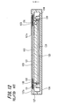
- FIG 12 shows the internal structure of an input device with liquid crystal display function according to related art.
- a protective plate 121 made of glass, for example is bonded to an upper case 127 with an adhesive 131.
- a silk-screen printed portion 130 for shielding light is provided on a lower surface of an end portion of the protective plate 121.
- a liquid crystal cell 122 is arranged in a lower case 128.
- a liquid crystal back light 123 and a liquid crystal back light unit 124 are fixed to the liquid crystal cell 122 via a metal bezel 126 by screwing screws 129 into bosses 134 in the lower case 128.
- a flat shaped digitizer 125 is arranged under a rear surface of the liquid crystal back light unit 124.
- FIG 13 shows the internal structure of an input device with liquid crystal display function according to another related art.
- a protective plate 141 is bonded to a liquid crystal cell 142 with an adhesive 151.
- a silk-screen printed portion 150 for shielding light is provided on a lower surface of an end portion of the protective plate 141.
- An upper case 147 is arranged so as to cover the end portion of the protective plate 141.
- a liquid crystal back light 143 and a liquid crystal back light unit 144 are fixed to the liquid crystal cell 142 via a metal bezel 146 by screwing screws 149 into the bosses in a lower case 148.
- a flat shaped digitizer 145 is arranged under a rear surface of the liquid crystal back light unit 144.
- an air layer 153 exists between the protective plate 141 and the liquid crystal cell 142.
- all assembly of the input device except for the process of bonding the protective plate 141 to the liquid crystal cell 142 with the adhesive 151, can be performed in a normal environment, instead of being performed in a clean room (see FIG 13 ).
- input operation is performed with, for example, a stylus pen (not shown). Specifically, input operation is performed by abutting the pen-tip of the stylus pen against the protective plates 121 or 141 to draw an illustration or write a character, just like drawing or writing with an ordinary ballpoint pen or pencil.
- input operation is detected and converted into digital data by the digitizers 125 or 145, and the digital data is inputted into a personal computer, a PDA, or the like, so that a handwriting input operation, such as drawing an illustration or writing a character, can be performed on the computer and the like.
- the protective plate 121 is bonded to the upper case 127 with the adhesive 131, and the liquid crystal cell 122 is fixed to the lower case 128 by the screws 129. Due to the play of the screws and the like, it is difficult to maintain the gap tolerance between the protective plate 121 and the liquid crystal cell 122 under an acceptable value. Further, it is difficult to determine a light shielding position alignment point 132 for performing position alignment between the silk-screen printed portion 130, the display area of the liquid crystal cell 122, and the metal bezel 126.
- the lower case 128 or 148 since all components have to be fixed to the lower case 128 or 148 with the screws 129 or 149, the lower case 128 or 148 needs to be formed with bosses 134 for receiving the screws 129 or 149.
- the lower case 128 is typically produced either by using a sheet metal process, or by using an injection molding process.
- the number of choices for the material and shape of the lower case 128 is limited.
- an object of the present invention to provide an input device with display function, which has a high degree of freedom in design, excellent operability, and in which position alignment for assembling components of the display module can be simply performed.
- an input device with display function includes: a transparent panel (protective plate) having a frame projecting substantially perpendicularly from one surface thereof; a flat panel display unit; and a flat sensor for detecting a position indicating operation performed on the other surface of the transparent panel.
- the flat panel display unit is housed in the frame such that a display surface of the flat panel display unit opposes the transparent panel.
- the flat sensor is also housed in the frame adjacent to the flat panel display unit. In this configuration, the flat panel display unit, the flat sensor, and the transparent panel are fixed to each other.
- the flat sensor may be located adjacent to the display surface of the flat panel display unit, so that the flat sensor is positioned between the transparent panel and the flat panel display unit.
- the flat sensor may be located adjacent to the opposite surface of the flat panel display unit, so that the flat panel display unit is positioned between the transparent panel and the flat sensor.
- the flat panel display unit may be a liquid crystal display unit including a liquid crystal cell and a liquid crystal back light unit, an organic EL display unit, a plasma display unit, or the like.
- the frame is provided on the lower surface side of the transparent panel to house and secure therein the flat panel display unit and the flat sensor, positioning and assembly of the transparent panel, the flat panel display unit, and the flat sensor can be easily and precisely performed.
- the frame projecting from the transparent panel is bonded to the transparent panel, preferably with an adhesive.
- the transparent panel is made of glass
- the frame is preferably made of a resin material.
- the transparent panel and the frame are integrally formed of a resin material.
- the flat sensor is located adjacent to another surface of the flat panel display unit opposite to the display surface such that the flat panel display unit is positioned between the transparent panel and the flat sensor.
- the flat sensor is an electromagnetic induction type sensor which detects a position indicating operation performed with a pen-like position indicator on the other surface of the transparent panel.
- the flat sensor is provided with a magnetic shield plate on a surface of the flat sensor opposite from the flat panel display unit.
- the flat sensor is a a capacitive type sensor which detects a position indicating operation performed by a finger of a user on the other surface of the transparent panel.
- the flat panel display unit is selected from a group consisting of a liquid crystal display unit, an organic EL display unit, and a plasma display unit.
- the present invention also relates to a method of assembling an input device with display function, especially as described in claim 9, while claims 10 to 15 relate to a specifically advantageous realization of this method.
- the frame projecting from the transparent panel is bonded to the transparent panel, preferably with an adhesive.
- the transparent panel and the frame are integrally formed of a resin material.
- the step of housing the flat sensor in the frame comprises placing the flat sensor adjacent to another surface of the flat panel display unit opposite to the display surface, such that the flat panel display unit is positioned between the transparent panel and the flat sensor.
- the flat sensor is provided with a magnetic shield plate on a surface of the flat sensor opposite from the flat panel display unit.
- FIGS. 1 to 11 Various embodiments of the present invention will be described below with reference to FIGS. 1 to 11 . Like components are denoted by like numerals throughout FIGS. 1 to 11 .
- FIG. 1 is a perspective view showing an overview of an input device with liquid crystal display function according to one embodiment of the present invention.
- the input device with liquid crystal display function includes a liquid crystal module 1 and a case 11.
- the liquid crystal module 1 includes a protective plate 2 as a transparent panel, a frame 3 projecting from a lower surface of the protective plate 2, and a metal bezel 4 covering an end portion of a lower surface of the frame 3.
- the protective plate 2 is made of, for example, transparent glass
- the frame 3 is made of, for example, a resin material.
- the metal bezel 4 has a substantially L-shaped cross section.
- a liquid crystal cell 6 and a digitizer 9 may be housed within the frame 3.
- the position of the liquid crystal cell 6 can be readily determined in X-direction and Y-direction relative to the frame 3.
- the present embodiment is described based on an example in which the frame 3 is directly secured to the protective plate 2, the present invention also includes a configuration in which a projection is formed on the lower surface of the protective plate 2 along the portion where the frame 3 is to be attached (see the area indicated by the dotted lines in FIG 1 ).
- the projection is provided to serve as a reference during assembly of various components, so as to reduce an assembling tolerance for the liquid crystal cell, a liquid crystal back light unit (which is to be described later), and the like.
- the case 11 includes an upper case 12 and a lower case 13.
- the upper case 12 and the lower case 13 have an opening 11a for housing the frame 3 of the liquid crystal module 1.
- a space for receiving the frame 3 is provided in a lower portion of the opening 11a of the upper case 12 (toward the side of the lower case).
- the upper case 12 has a recessed portion 12a formed in the periphery of the opening 11a.
- the recessed portion 12a is formed so that when the liquid crystal module 1 is housed in the case 11, the upper surface 12b of the upper case 12 and the upper surface 2a of the protective plate 2 of the liquid crystal module 1 substantially have the same height (in Z-direction).
- a portion of the protective plate 2 outside of (peripheral to) the frame 3 is fitted into the recessed portion 12a of the upper case 12.
- the lower surface of the protective plate 2 is fixed to the recessed portion 12a with an adhesive or the like. Since no offset (stepped portion) is formed between the upper surface 12b of the upper case 12 and the upper surface 2a of the protective plate 2, the input device with liquid crystal display function has good operability.
- the protective plate 2 is shaped so that it can be closely fitted within the opening 11a of the upper case 12.
- the protective plate 2 By shaping the protective plate 2 in such a manner, no gap is generated in the horizontal direction (i.e., in X-axis direction and Y-axis direction), and the liquid crystal module 1 can be closely fitted into the case 11.
- a user performs a handwriting operation with a stylus pen (not shown)
- operability will not be impaired when the pen-tip of the stylus pen is drawn over the boundary portion between the protective plate 2 and the upper case 12.
- FIG 2 is a cross section taken along line a-a' of the input device shown in FIG 1 .
- a silk-screen printed portion 5 for shielding light is provided on a lower surface 2b of the protective plate 2, which may be made of transparent glass, for example.
- the frame 3 configured with a resin-made main body 3a is attached to the protective plate 2 by applying an adhesive to a bonding surface 3b, such that the silk-screen printed portion 5 is sandwiched between the protective plate 2 and the frame 3. Additionally, the frame 3 is fixed to a predetermined position inward from an end portion 2c of the protective plate 2.
- the main body 3 a of the frame 3 is configured so as to form a housing portion 3c for housing a liquid crystal cell 6 (which is to be described later) and the like inside the frame 3.
- the liquid crystal cell 6 is housed in the housing portion 3c so that a display surface 6a thereof closely contacts the lower surface 2b of the protective plate 2.
- the position of the liquid crystal cell 6 can be determined by arranging the frame 3 to a desired position on the lower surface 2b of the protective plate 2. Further, due to the placement of the silk-screen printed portion 5, the bonding surface 3b where the protective plate 2 and the frame 3 are bonded together may be made invisible (concealed). The frame 3 extending from the protective plate 2 facilitates proper positioning of the liquid crystal cell, and thus alignment between the silk-screen printed portion 5 of the protective plate 2 and the liquid crystal cell 6 is also facilitated. Note that, although the silk-screen printed portion 5 is arranged between the lower surface 2b of the protective plate 2 and the frame 3 in the present embodiment, the silk-screen printed portion 5 may also be arranged on the upper surface 2a of the protective plate 2.
- the recessed portion 12a is formed so that, when the liquid crystal module 1 is housed in the case 11, the upper surface 12b of the upper case 12 and the upper surface 2a of the protective plate 2 have substantially the same height (in Z-direction). Since the opening 11a of the upper case 12 is shaped corresponding to the shape of the protective plate 2, after the protective plate 2 is fitted into the recessed portion 12a of the upper case 12, the protective plate 2 can be fixed to the upper case 12 merely by fixing the connecting portion 21 of the protective plate 2 to the recessed portion 12a with an adhesive or the like. As a result, substantially no clearance or offset will be generated between the protective plate 2 and the upper case 12.
- the lower case 13 does not have to be made of a magnesium alloy or other material, as in the prior art. Further, the lower case 13 can be produced without using sheet metal processing. As a result, the number of choices of the material and shape for the lower case is increased, and the degree of freedom in design of the position detecting device with liquid crystal display function can be increased.
- the liquid crystal cell 6, the liquid crystal back light unit 8, and the digitizer 9 are all housed in the housing portion 3c of the frame 3, and if the protective plate 2 and the liquid crystal cell 6, the liquid crystal cell 6 and the liquid crystal back light unit 8, and the liquid crystal back light unit 8 and the digitizer 9 are respectively fixed to each other with an adhesive or the like, the metal bezel 4 will be unnecessary. In other words, the liquid crystal cell 6, the liquid crystal back light unit 8, and the digitizer 9 can be fixed either with the metal bezel 4, or with an adhesive or the like.
- a shield plate (not shown) formed of a magnetic material (magnetic circuit plate) may also be used instead of the metal bezel 4 having a substantially L-shaped cross section.
- the shield plate provided on a rear surface of the digitizer 9
- the magnetic circuit plate is formed of a relatively soft material
- a reinforcing plate (not shown) may be provided on the lower surface (i.e., the surface facing the bottom of the lower case 13) of the magnetic circuit plate, and the reinforcing plate may be fixed to the frame 3 by screws or the like.
- the upper case 12 and the lower case 13 may also be integrally formed.
- a light shielding film can be employed or a light shielding ink can be applied.
- a thin fluorescent display tube, an organic EL (organic Electro-Luminescence), an organic light-emitting diode, or a Light Emitting Polymer may be used instead of the liquid crystal cell 6, the liquid crystal back light 7, and the liquid crystal back light unit 8.
- the protective plate 2 is made of glass or the like
- the frame 3 is made of resin or the like
- the protective plate 2 and the frame 3 are fixed to each other through the bonding surface 3b with adhesive, screws, or another fixing mechanism.
- the protective plate 2 and the frame 3 may be integrally formed of the same material, such as a reinforced plastic with transparency.
- the present embodiment is described using an example in which the frame 3 has a shape formed by four faces perpendicularly extending from the protective plate 2, the present invention is not limited to this example.
- the present invention includes a configuration in which, among the aforesaid four faces, two opposing faces are arranged on the side of the protective plate 2 and the other two opposing faces are arranged on the side of the metal bezel 4, so that upon assembly of the liquid crystal module 1, the four faces are combined to together form the frame 3, which then defines the position of every component.
- various embodiments of the present invention essentially contemplate an input device having a flat panel display unit, in which input operation can be performed on a (transparent) panel disposed in front of the flat panel display unit.
- the flat panel display unit and the panel disposed in front of the flat panel display unit are positioned with respect to each other based on a frame extending from the panel and are integrally fixed to each other.
- the panel is generally, but is not limited to, a protective panel for protecting the flat panel display unit. However, since the panel is disposed in front of the flat panel display unit, the panel is required to have a high optical transparency. Further, apart from the liquid crystal display unit, other displays such as an organic EL display, a plasma display, or the like may also be used as the flat panel display unit.
- FIG 3 is an exploded perspective view of an embodiment of the present invention showing how the liquid crystal module 1 is assembled.
- the frame 3 is first fixed to a frame bonding surface 32 of the protective plate 2 with an adhesive or the like.
- the frame bonding surface 32 is placed within a range associated with the silk-screen printed portion 5 provided on the lower surface of the end portion 2c of the protective plate 2.
- the frame bonding surface 32 is provided on the protective plate 2 in a position inside the connecting portion 21 shown in FIG 2 .
- the liquid crystal cell 6 is positioned within the housing portion 3c inside the frame 3. Further, the lower surface of the protective plate 2 and the upper surface 6a of the liquid crystal cell 6 are bonded to each other with an adhesive or the like. Since the end portion 6c of the liquid crystal cell 6 is guided to a proper position inside the frame 3, the end portion 6c of the liquid crystal cell 6 is positioned within a range associated with the silk-screen printed portion 5 provided on the lower surface of the end portion 2c of the protective plate 2. This allows the end portion 6c of the liquid crystal cell 6 to be positioned in an invisible (concealed) manner.
- the gap between the protective plate 2 and the liquid crystal cell 6 may be closed by placing a filler between the protective plate 2 and the liquid crystal cell 6. Further, the gap between the protective plate 2 and the liquid crystal cell 6 may also be closed by using a so-called optical bonding technology in which a filler having high transparency is placed between the protective plate 2 and the liquid crystal cell 6. For example, a silicon-based gel or adhesive is filled between the protective plate 2 and the liquid crystal cell 6 so that optical properties of the interface between the protective plate 2 and the liquid crystal cell 6 can be improved.
- the liquid crystal back light unit 8 is also positioned within the housing portion 3c inside the frame 3. Further, a lower surface of the liquid crystal cell 6 and an upper surface of the liquid crystal back light unit 8 are bonded to each other with an adhesive or the like. Although not shown in the attached drawings, the liquid crystal back light 7 is provided in an end portion of the liquid crystal back light unit 8 so that the light can be guided through the liquid crystal back light unit 8.
- the digitizer (sensor) 9 is positioned within the housing portion 3c, also inside the frame 3. As a result, alignment of the liquid crystal cell 6, the liquid crystal back light unit 8, and the digitizer 9 with respect to the protective plate 2 can be easily performed.
- the lower surface of the liquid crystal back light unit 8 and a front surface 9b of the digitizer 9 are bonded to each other with an adhesive or the like. Additionally, alignment may also be performed by using a jig (not shown) previously arranged on the protective plate 2 in a position inside the connecting portion 21 shown in FIG 2 , the jig being provided to guide the frame 3 into position.
- the rear surface of the digitizer 9 may be fixed, via the metal bezel 4 having the substantially L-shaped cross section, to the frame 3 by inserting four screws 35, 36, 35', and 36' into four square holes 33, 34, 33', and 34', respectively, of the frame 3 and then tightening the screws.
- the assembly operation begins with fixing the protective plate 2 to the frame 3. Note that, as has been mentioned above, in the case where the protective plate 2 and the frame 3 are integrally formed, the step of fixing the protective plate 2 and the frame 3 to each other may be skipped.
- the liquid crystal cell 6 can be properly positioned with reference to the frame 3, and the positioned liquid crystal cell 6 is fixed to the protective plate 2. Only this step is required to be performed in a clean room, and the other steps may be performed in a normal environment. Further, the liquid crystal back light unit 8 is fixed to the liquid crystal cell 6, and the digitizer 9 is fixed to the liquid crystal back light unit 8. Finally, the end portion 9a of the digitizer 9 is fixed to the frame 3 using the metal bezel 4, which has a substantially L-shaped cross section.
- FIGS. 4A to 8 Further embodiments of the present invention will be described below with reference to FIGS. 4A to 8 .
- FIGS. 4A and 4B show an embodiment of a frame 41 which includes a brim (wide) portion 42, wherein FIG 4A is a perspective view and FIG 4B is an enlarged cross section taken along line b-b' of FIG. 4A .
- the frame may also have a configuration in which, compared to the width of the frame main body 41a, the portion to be bonded to the protective plate 2 has a larger width.
- the frame 41 has the main body 41a, the wide portion 42 continuing from the main body 41a, and a bonding surface 41b formed on an end face of the wide portion 42.
- the width (i.e., the length in the direction parallel to the protective plate 2) of the wide portion 42 increases gradually from the main body 41a toward the protective plate 2, so that the width of the wide portion 42 is greater than that of the main body 41a.
- the width of the wide portion 42 is set so that the wide portion 42 falls within a range associated with the silk-screen printed portion 5.
- FIGS. 5A and 5B show another embodiment of a frame which is integrally formed from a frame portion 52 and a protective plate 51, wherein FIG 5A is a perspective view and FIG 5B is a cross section taken along line c-c' of FIG. 5A .
- the present invention may also include a configuration in which the protective plate and the frame are integrally formed of a resin material, for example.
- a protective plate 51 and a frame portion 52 are integrally formed to form a frame having a substantially T-shaped cross section.
- the silk-screen printed portion 5 is arranged on an upper surface (a surface on which a user performs input operation) of the protective plate 51 so as to cover an area where the frame portion 52 meets the protective plate 51.
- FIGS. 6A and 6B show another embodiment of the present invention, comprising a frame 61, which has a tapered portion 62, wherein FIG. 6A is a perspective view and FIG. 6B is an enlarged cross section taken along line d-d' of FIG 6A .
- the present invention may also include a configuration in which the frame has a tapering shape as described below.
- the frame 61 includes the main body portion 61a forming four sides of the frame 61, wherein each pair of sides of the main body portions 61a opposing each other has a tapered portion 62 formed at least in an inner wall portion thereof.
- the tapered portion 62 is formed in a manner so that the width of the housing portion 3c becomes gradually greater, from the bonding surface 3b at the upper end portion toward the lower end portion 61b.
- the liquid crystal cell 6, the liquid crystal back light unit 8, and the thin digitizer 9 can be easily inserted from the side of the lower end portion 61b, and further, the inserted components can be rigidly secured.
- the tapered portion 62 is formed in both the inner wall portion and outer wall portion of each of the sides of the main body portion 61a of the frame 61.
- the tapered portion 62 may also be formed in the inner wall portion only.
- a plurality of tapered portions 62 may be formed in a stepwise manner, forming steps along the inner wall portion of the frame 61 instead of a smooth inner wall portion of the frame 61.
- the liquid crystal cell 6, the liquid crystal back light unit 8, and the digitizer 9 are inserted sequentially in this order along the inner wall of the tapered portion 62 from the lower end portion 61b toward the upper end portion of the main body portion 61a of the frame 61 (i.e., toward the bonding surface 3b).
- the sizes (i.e., the widths) of the liquid crystal cell 6, the liquid crystal back light unit 8, and the digitizer 9 need to be set corresponding to the tapering shape of the tapered portion 62.
- FIG 7 is a view showing another embodiment of the lower case 71, which has projections 72.
- the present invention may include a configuration in which the lower case is provided with the projections as described below.
- a plurality of projections 72 are arranged on an inner bottom 71a of a lower case 71.
- the width and height of each of the plurality of projections 72 are set so that the metal bezel 4 and the lower surface of the digitizer 9 of the liquid crystal module 1 shown in FIG 2 can be supported by the projections 72.
- the strength of the protective plate 2 is reinforced and the protective plate 2 is resistant to bending, even when the user puts his hand on the upper surface 2a of the protective plate 2 during an input operation, or even when the user strongly presses the protective plate 2 during an input operation with the stylus pen.
- the liquid crystal module 1 can be prevented from being bent downward.
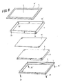
- FIG 8 is an exploded perspective view showing assembly of the liquid crystal module according to another embodiment of the present invention.
- the digitizer (sensor) 9 is an electromagnetic induction type digitizer which operates based on electromagnetic resonance technology
- the digitizer may also be a capacitive type sensor as described below.
- the capacitive type sensor is adapted to detect the position indicated by a stylus pen (not shown) or by a finger of the user.
- a well-known example of the capacitive type sensor is the one which includes a transparent electrode formed using an ITO film (Indium Tin Oxide film).
- a sensor is usable only when the distance to the object-to-be-detected (i.e., the finger of the user) is small, such as in the case of the capacitive type sensor, the sensor needs to be disposed as close to the protective plate 2 as possible. For this reason, in the embodiment shown in FIG. 8 , a sensor 81 is arranged between the protective plate 2 and the liquid crystal cell 6. Since other structures are identical to those of the example shown in FIG 3 , further description of FIG 8 will be omitted.
- other sensor(s) such as a sensor using a resistance film, may be additionally arranged on the upper surface of the protective plate 2.
- contact of the stylus pen can be detected on the upper surface of the protective plate 2.
- FIG 9 shows an example of applying the liquid crystal module to a general-purpose personal computer.
- a liquid crystal module 93 according to the aforesaid embodiments is incorporated into a display 92 connected to a computer main body 91.
- the user uses a stylus pen 94 to draw lines or points on the screen of the liquid crystal module 93.
- FIG. 9 shows an example in which the personal computer and the display 92 are separated from each other, the present invention may also be applied to a computer in which the display 92 and the main body 91 are integrated, such as a laptop computer.
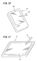
- FIG 10 shows an example of applying the liquid crystal module 102 to a PDA (personal digital assistant) 101 as a portable electronic device.
- PDA personal digital assistant
- a liquid crystal module 102 is incorporated into a display panel of a PDA 101.
- the user uses a stylus pen 103 to draw lines or points on the screen of the liquid crystal module 102.
- the portable electronic device may also be a different device, such as a cell-phone, and is not limited to the PDA.
- FIG 11 shows an example of applying the liquid crystal module to a tablet as a portable electronic device.
- a liquid crystal module 112 is arranged on a display panel of a tablet 111.
- the user uses a stylus pen 113 to draw lines or points on the screen of the liquid crystal module 112.
- coordinate input operations can be performed by applying the liquid crystal module, according to various embodiments of the present invention, to a display or display panel of various electronic devices.
Landscapes
- Engineering & Computer Science (AREA)
- Theoretical Computer Science (AREA)
- General Engineering & Computer Science (AREA)
- Physics & Mathematics (AREA)
- General Physics & Mathematics (AREA)
- Human Computer Interaction (AREA)
- Computer Hardware Design (AREA)
- Nonlinear Science (AREA)
- Mathematical Physics (AREA)
- Chemical & Material Sciences (AREA)
- Crystallography & Structural Chemistry (AREA)
- Computer Networks & Wireless Communication (AREA)
- Optics & Photonics (AREA)
- Position Input By Displaying (AREA)
- Devices For Indicating Variable Information By Combining Individual Elements (AREA)
- Liquid Crystal (AREA)
Abstract
Description
- The present invention relates to an input device with display function for performing input operation to a digitizer (a coordinate position inputting sensor) based on, for example, an electromagnetic resonance technology.
- In recent years, there has been proposed an input device with liquid crystal display function to be applied to an electronic device such as a personal computer, a PDA (personal digital assistant) or the like. There also has been proposed a position detecting device in which a shield plate is used (see Japanese Unexamined Patent Application Publication No.
2005-275381 2006-309308 -
FIG 12 shows the internal structure of an input device with liquid crystal display function according to related art. In such an input device, aprotective plate 121 made of glass, for example, is bonded to anupper case 127 with an adhesive 131. A silk-screen printedportion 130 for shielding light is provided on a lower surface of an end portion of theprotective plate 121. - A
liquid crystal cell 122 is arranged in alower case 128. A liquidcrystal back light 123 and a liquid crystalback light unit 124 are fixed to theliquid crystal cell 122 via ametal bezel 126 by screwingscrews 129 intobosses 134 in thelower case 128. A flat shapeddigitizer 125 is arranged under a rear surface of the liquid crystalback light unit 124. - As seen in
FIG 12 , since anair layer 133 exists between theliquid crystal cell 122 attached to thelower case 128 and theprotective plate 121 attached to theupper case 127, all assembly of the input device, as seen inFIG 12 , is performed in a clean room so that no dust and the like is mixed into theair layer 133. -
FIG 13 shows the internal structure of an input device with liquid crystal display function according to another related art. In such an input device, aprotective plate 141 is bonded to aliquid crystal cell 142 with an adhesive 151. A silk-screen printedportion 150 for shielding light is provided on a lower surface of an end portion of theprotective plate 141. Anupper case 147 is arranged so as to cover the end portion of theprotective plate 141. - A liquid
crystal back light 143 and a liquid crystalback light unit 144 are fixed to theliquid crystal cell 142 via ametal bezel 146 by screwingscrews 149 into the bosses in alower case 148. A flat shapeddigitizer 145 is arranged under a rear surface of the liquid crystalback light unit 144. - As seen in
FIG 13 , anair layer 153 exists between theprotective plate 141 and theliquid crystal cell 142. In this case, all assembly of the input device, except for the process of bonding theprotective plate 141 to theliquid crystal cell 142 with the adhesive 151, can be performed in a normal environment, instead of being performed in a clean room (seeFIG 13 ). In the input devices with liquid crystal display function having the aforesaid arrangements, input operation is performed with, for example, a stylus pen (not shown). Specifically, input operation is performed by abutting the pen-tip of the stylus pen against theprotective plates digitizers - In the arrangement shown in
FIG. 12 , theprotective plate 121 is bonded to theupper case 127 with theadhesive 131, and theliquid crystal cell 122 is fixed to thelower case 128 by thescrews 129. Due to the play of the screws and the like, it is difficult to maintain the gap tolerance between theprotective plate 121 and theliquid crystal cell 122 under an acceptable value. Further, it is difficult to determine a light shieldingposition alignment point 132 for performing position alignment between the silk-screen printedportion 130, the display area of theliquid crystal cell 122, and themetal bezel 126. - Further, in the arrangement shown in
FIG 13 , since all components are fixed to thelower case 148 by thescrews 149, if theprotective plate 141 is attached to theupper case 147 with low accuracy, agap 152 will be generated between theprotective plate 141 and theupper case 147. Also, similar to the arrangement shown inFIG. 12 , since all components are fixed to thelower case 148 by thescrews 149, there is a concern that theupper case 147 may be offset from the end portion(s) of theprotective plate 141 in the thickness direction (i.e., in Z-direction, seeFIG. 12 ). - In the case of an ordinary liquid crystal display device with no input function, even if the offset or the
gap 152 is generated, it will cause no problem in function, though it does cause some problems in appearance. However, in the case of an input device with liquid crystal display function, since a user performs handwriting input operation on the upper surface of theprotective plate gap 152 or fall into thegap 152. Further, if an offset is generated between anupper surface 121a of theprotective plate 121 and anupper surface 127a of theupper case 127, operability will be impaired since the user's hand may touch the offsetting (stepping) portion. - Further, in the arrangements shown in
FIGS. 12 and13 , since all components have to be fixed to thelower case screws lower case bosses 134 for receiving thescrews bosses 134, thelower case 128 is typically produced either by using a sheet metal process, or by using an injection molding process. Thus, the number of choices for the material and shape of thelower case 128 is limited. - Accordingly, it is an object of the present invention to provide an input device with display function, which has a high degree of freedom in design, excellent operability, and in which position alignment for assembling components of the display module can be simply performed.
- To achieve the above-mentioned object, an input device with display function according to an aspect of the present invention includes: a transparent panel (protective plate) having a frame projecting substantially perpendicularly from one surface thereof; a flat panel display unit; and a flat sensor for detecting a position indicating operation performed on the other surface of the transparent panel. The flat panel display unit is housed in the frame such that a display surface of the flat panel display unit opposes the transparent panel. The flat sensor is also housed in the frame adjacent to the flat panel display unit. In this configuration, the flat panel display unit, the flat sensor, and the transparent panel are fixed to each other.
- The flat sensor may be located adjacent to the display surface of the flat panel display unit, so that the flat sensor is positioned between the transparent panel and the flat panel display unit. Alternatively, the flat sensor may be located adjacent to the opposite surface of the flat panel display unit, so that the flat panel display unit is positioned between the transparent panel and the flat sensor.
- The flat panel display unit may be a liquid crystal display unit including a liquid crystal cell and a liquid crystal back light unit, an organic EL display unit, a plasma display unit, or the like.
- According to the present invention, since the frame is provided on the lower surface side of the transparent panel to house and secure therein the flat panel display unit and the flat sensor, positioning and assembly of the transparent panel, the flat panel display unit, and the flat sensor can be easily and precisely performed.
- According to one embodiment of the input device, the frame projecting from the transparent panel is bonded to the transparent panel, preferably with an adhesive.
- In a preferred embodiment the transparent panel is made of glass, and the frame is preferably made of a resin material.
- Preferably the transparent panel and the frame are integrally formed of a resin material.
- In a preferred embodiment the flat sensor is located adjacent to another surface of the flat panel display unit opposite to the display surface such that the flat panel display unit is positioned between the transparent panel and the flat sensor.
- In a further preferred embodiment, the flat sensor is an electromagnetic induction type sensor which detects a position indicating operation performed with a pen-like position indicator on the other surface of the transparent panel.
- In one preferred embodiment the flat sensor is provided with a magnetic shield plate on a surface of the flat sensor opposite from the flat panel display unit.
- Preferably the flat sensor is a a capacitive type sensor which detects a position indicating operation performed by a finger of a user on the other surface of the transparent panel.
- In one preferred embodiment the flat panel display unit is selected from a group consisting of a liquid crystal display unit, an organic EL display unit, and a plasma display unit.
- The present invention also relates to a method of assembling an input device with display function, especially as described in
claim 9, while claims 10 to 15 relate to a specifically advantageous realization of this method. - According to a preferred realization of the method the frame projecting from the transparent panel is bonded to the transparent panel, preferably with an adhesive.
- Preferably the transparent panel and the frame are integrally formed of a resin material.
- According to a preferred realization of the method, the step of housing the flat sensor in the frame comprises placing the flat sensor adjacent to another surface of the flat panel display unit opposite to the display surface, such that the flat panel display unit is positioned between the transparent panel and the flat sensor.
- Furthermore, preferably the flat sensor is provided with a magnetic shield plate on a surface of the flat sensor opposite from the flat panel display unit.
-
-
FIG 1 is a perspective view showing an overview of an input device with liquid crystal display function according to an embodiment of the present invention; -
FIG 2 is a cross section taken along line a-a' of the input device shown inFIG 1 ; -
FIG 3 is an exploded perspective view showing assembly of a liquid crystal module of the input device; -
FIGS. 4A and 4B show another embodiment of a frame which includes a brim portion, whereinFIG 4A is a perspective view andFIG 4B is an enlarged cross section taken along line b-b' ofFIG 4A ; -
FIGS. 5A and 5B show yet another embodiment of a frame which is integrally formed with a protective plate, whereinFIG 5A is a perspective view andFIG 5B is an enlarged cross section taken along line c-c' ofFIG. 5A ; -
FIGS. 6A and 6B show a further embodiment of a frame which has a tapered portion, whereinFIG 6A is a perspective view andFIG 6B is an enlarged cross section taken along line d-d' ofFIG 6A ; -
FIG 7 is a view showing an embodiment of a lower case that has projections; -
FIG 8 is an exploded perspective view showing assembly of the liquid crystal module according to another embodiment; -
FIG 9 shows a general-purpose personal computer including a liquid crystal module of the present invention; -
FIG 10 shows a PDA (personal digital assistant) as a portable electronic device including a liquid crystal module of the present invention; -
FIG 11 shows a tablet as a portable electronic device including a liquid crystal module of the present invention; -
FIG. 12 is a view showing the internal structure of an input device with liquid crystal display function according to the prior art; and -
FIG 13 is a view showing the internal structure of an input device with liquid crystal display function according to the prior art. - Various embodiments of the present invention will be described below with reference to
FIGS. 1 to 11 . Like components are denoted by like numerals throughoutFIGS. 1 to 11 . -
FIG. 1 is a perspective view showing an overview of an input device with liquid crystal display function according to one embodiment of the present invention. - As shown in
FIG 1 , the input device with liquid crystal display function according to the present embodiment includes a liquid crystal module 1 and acase 11. The liquid crystal module 1 includes aprotective plate 2 as a transparent panel, aframe 3 projecting from a lower surface of theprotective plate 2, and ametal bezel 4 covering an end portion of a lower surface of theframe 3. Theprotective plate 2 is made of, for example, transparent glass, and theframe 3 is made of, for example, a resin material. Themetal bezel 4 has a substantially L-shaped cross section. - A
liquid crystal cell 6 and a digitizer 9 (which are to be described later, seeFIG. 2 ) may be housed within theframe 3. As a result, the position of theliquid crystal cell 6 can be readily determined in X-direction and Y-direction relative to theframe 3. While the present embodiment is described based on an example in which theframe 3 is directly secured to theprotective plate 2, the present invention also includes a configuration in which a projection is formed on the lower surface of theprotective plate 2 along the portion where theframe 3 is to be attached (see the area indicated by the dotted lines inFIG 1 ). The projection is provided to serve as a reference during assembly of various components, so as to reduce an assembling tolerance for the liquid crystal cell, a liquid crystal back light unit (which is to be described later), and the like. - The
case 11 includes anupper case 12 and alower case 13. Theupper case 12 and thelower case 13 have anopening 11a for housing theframe 3 of the liquid crystal module 1. A space for receiving theframe 3 is provided in a lower portion of theopening 11a of the upper case 12 (toward the side of the lower case). - Further, the
upper case 12 has a recessedportion 12a formed in the periphery of theopening 11a. The recessedportion 12a is formed so that when the liquid crystal module 1 is housed in thecase 11, theupper surface 12b of theupper case 12 and theupper surface 2a of theprotective plate 2 of the liquid crystal module 1 substantially have the same height (in Z-direction). At this time, a portion of theprotective plate 2 outside of (peripheral to) theframe 3 is fitted into the recessedportion 12a of theupper case 12. Further, the lower surface of theprotective plate 2 is fixed to the recessedportion 12a with an adhesive or the like. Since no offset (stepped portion) is formed between theupper surface 12b of theupper case 12 and theupper surface 2a of theprotective plate 2, the input device with liquid crystal display function has good operability. - The
protective plate 2 is shaped so that it can be closely fitted within theopening 11a of theupper case 12. By shaping theprotective plate 2 in such a manner, no gap is generated in the horizontal direction (i.e., in X-axis direction and Y-axis direction), and the liquid crystal module 1 can be closely fitted into thecase 11. As a result, when a user performs a handwriting operation with a stylus pen (not shown), operability will not be impaired when the pen-tip of the stylus pen is drawn over the boundary portion between theprotective plate 2 and theupper case 12. - Next, the internal structure of the input device with liquid crystal display function according to the present embodiment will be described below.
-
FIG 2 is a cross section taken along line a-a' of the input device shown inFIG 1 . - As shown in
FIG 2 , in the liquid crystal module 1, a silk-screen printedportion 5 for shielding light is provided on alower surface 2b of theprotective plate 2, which may be made of transparent glass, for example. Theframe 3 configured with a resin-mademain body 3a is attached to theprotective plate 2 by applying an adhesive to abonding surface 3b, such that the silk-screen printedportion 5 is sandwiched between theprotective plate 2 and theframe 3. Additionally, theframe 3 is fixed to a predetermined position inward from anend portion 2c of theprotective plate 2. - The
main body 3 a of theframe 3 is configured so as to form ahousing portion 3c for housing a liquid crystal cell 6 (which is to be described later) and the like inside theframe 3. Theliquid crystal cell 6 is housed in thehousing portion 3c so that adisplay surface 6a thereof closely contacts thelower surface 2b of theprotective plate 2. - The position of the
liquid crystal cell 6 can be determined by arranging theframe 3 to a desired position on thelower surface 2b of theprotective plate 2. Further, due to the placement of the silk-screen printedportion 5, thebonding surface 3b where theprotective plate 2 and theframe 3 are bonded together may be made invisible (concealed). Theframe 3 extending from theprotective plate 2 facilitates proper positioning of the liquid crystal cell, and thus alignment between the silk-screen printedportion 5 of theprotective plate 2 and theliquid crystal cell 6 is also facilitated. Note that, although the silk-screen printedportion 5 is arranged between thelower surface 2b of theprotective plate 2 and theframe 3 in the present embodiment, the silk-screen printedportion 5 may also be arranged on theupper surface 2a of theprotective plate 2. - A liquid crystal back light 7 and a liquid crystal back
light unit 8, such as a light guiding plate, are provided on arear surface 6b of theliquid crystal cell 6, and a digitizer (sensor) 9 is provided under arear surface 8a of the liquid crystal backlight unit 8. Further, anend portion 9a of thedigitizer 9 is fixed to theframe 3, which may be made of resin or the like, using themetal bezel 4 having a substantially L-shaped cross section. - Since the joining surface of the
protective plate 2 is brought into close contact with the joining surface of thedisplay surface 6a of theliquid crystal cell 6, all processes, except for the process of bringing theprotective plate 2 into close contact with theliquid crystal cell 6, can be performed in a normal environment, instead of being performed in a clean room. - A connecting
portion 21, which is located outside of thebonding surface 3b where theprotective plate 2 and theframe 3 are bonded together, is fitted into the recessedportion 12a of theupper case 12. Further, the connectingportion 21 is brought into contact with and fixed to the recessedportion 12a of theupper case 12. - As has been mentioned above, the recessed
portion 12a is formed so that, when the liquid crystal module 1 is housed in thecase 11, theupper surface 12b of theupper case 12 and theupper surface 2a of theprotective plate 2 have substantially the same height (in Z-direction). Since theopening 11a of theupper case 12 is shaped corresponding to the shape of theprotective plate 2, after theprotective plate 2 is fitted into the recessedportion 12a of theupper case 12, theprotective plate 2 can be fixed to theupper case 12 merely by fixing the connectingportion 21 of theprotective plate 2 to the recessedportion 12a with an adhesive or the like. As a result, substantially no clearance or offset will be generated between theprotective plate 2 and theupper case 12. - Additionally, since it is not required to fix the liquid crystal module 1 to the
lower case 13 by screws, it is not necessary to form bosses in thelower case 13 to install theliquid crystal cell 6 or the like. Thus, thelower case 13 does not have to be made of a magnesium alloy or other material, as in the prior art. Further, thelower case 13 can be produced without using sheet metal processing. As a result, the number of choices of the material and shape for the lower case is increased, and the degree of freedom in design of the position detecting device with liquid crystal display function can be increased. - Additionally, when the
liquid crystal cell 6, the liquid crystal backlight unit 8, and thedigitizer 9 are all housed in thehousing portion 3c of theframe 3, and if theprotective plate 2 and theliquid crystal cell 6, theliquid crystal cell 6 and the liquid crystal backlight unit 8, and the liquid crystal backlight unit 8 and thedigitizer 9 are respectively fixed to each other with an adhesive or the like, themetal bezel 4 will be unnecessary. In other words, theliquid crystal cell 6, the liquid crystal backlight unit 8, and thedigitizer 9 can be fixed either with themetal bezel 4, or with an adhesive or the like. - In another embodiment, a shield plate (not shown) formed of a magnetic material (magnetic circuit plate) may also be used instead of the
metal bezel 4 having a substantially L-shaped cross section. By using the shield plate (provided on a rear surface of the digitizer 9), it is possible to provide an input device with liquid crystal display function in which the position of the entire rear surface of thedigitizer 9 can be defined by theframe 3, and which is less susceptible to the influence of external noise. Since the magnetic circuit plate is formed of a relatively soft material, a reinforcing plate (not shown) may be provided on the lower surface (i.e., the surface facing the bottom of the lower case 13) of the magnetic circuit plate, and the reinforcing plate may be fixed to theframe 3 by screws or the like. - In another embodiment of the present invention, the
upper case 12 and thelower case 13 may also be integrally formed. Further, instead of employing the silk-screen printedportion 5, a light shielding film can be employed or a light shielding ink can be applied. Further, a thin fluorescent display tube, an organic EL (organic Electro-Luminescence), an organic light-emitting diode, or a Light Emitting Polymer may be used instead of theliquid crystal cell 6, the liquid crystal back light 7, and the liquid crystal backlight unit 8. - In the present embodiment, the
protective plate 2 is made of glass or the like, theframe 3 is made of resin or the like, and theprotective plate 2 and theframe 3 are fixed to each other through thebonding surface 3b with adhesive, screws, or another fixing mechanism. However, theprotective plate 2 and theframe 3 may be integrally formed of the same material, such as a reinforced plastic with transparency. - Further, although the present embodiment is described using an example in which the
frame 3 has a shape formed by four faces perpendicularly extending from theprotective plate 2, the present invention is not limited to this example. For example, the present invention includes a configuration in which, among the aforesaid four faces, two opposing faces are arranged on the side of theprotective plate 2 and the other two opposing faces are arranged on the side of themetal bezel 4, so that upon assembly of the liquid crystal module 1, the four faces are combined to together form theframe 3, which then defines the position of every component. - In summary, various embodiments of the present invention essentially contemplate an input device having a flat panel display unit, in which input operation can be performed on a (transparent) panel disposed in front of the flat panel display unit. The flat panel display unit and the panel disposed in front of the flat panel display unit are positioned with respect to each other based on a frame extending from the panel and are integrally fixed to each other. The panel is generally, but is not limited to, a protective panel for protecting the flat panel display unit. However, since the panel is disposed in front of the flat panel display unit, the panel is required to have a high optical transparency. Further, apart from the liquid crystal display unit, other displays such as an organic EL display, a plasma display, or the like may also be used as the flat panel display unit.
- Next, the process of assembling the liquid crystal module 1 will be described below.
-
FIG 3 is an exploded perspective view of an embodiment of the present invention showing how the liquid crystal module 1 is assembled. - As shown in
FIG. 3 , in the case where theprotective plate 2 and theframe 3 are individual components separated from each other, theframe 3 is first fixed to aframe bonding surface 32 of theprotective plate 2 with an adhesive or the like. Theframe bonding surface 32 is placed within a range associated with the silk-screen printedportion 5 provided on the lower surface of theend portion 2c of theprotective plate 2. Theframe bonding surface 32 is provided on theprotective plate 2 in a position inside the connectingportion 21 shown inFIG 2 . - Next, the
liquid crystal cell 6 is positioned within thehousing portion 3c inside theframe 3. Further, the lower surface of theprotective plate 2 and theupper surface 6a of theliquid crystal cell 6 are bonded to each other with an adhesive or the like. Since theend portion 6c of theliquid crystal cell 6 is guided to a proper position inside theframe 3, theend portion 6c of theliquid crystal cell 6 is positioned within a range associated with the silk-screen printedportion 5 provided on the lower surface of theend portion 2c of theprotective plate 2. This allows theend portion 6c of theliquid crystal cell 6 to be positioned in an invisible (concealed) manner. - The gap between the
protective plate 2 and theliquid crystal cell 6 may be closed by placing a filler between theprotective plate 2 and theliquid crystal cell 6. Further, the gap between theprotective plate 2 and theliquid crystal cell 6 may also be closed by using a so-called optical bonding technology in which a filler having high transparency is placed between theprotective plate 2 and theliquid crystal cell 6. For example, a silicon-based gel or adhesive is filled between theprotective plate 2 and theliquid crystal cell 6 so that optical properties of the interface between theprotective plate 2 and theliquid crystal cell 6 can be improved. - Next, the liquid crystal back
light unit 8 is also positioned within thehousing portion 3c inside theframe 3. Further, a lower surface of theliquid crystal cell 6 and an upper surface of the liquid crystal backlight unit 8 are bonded to each other with an adhesive or the like. Although not shown in the attached drawings, the liquid crystal back light 7 is provided in an end portion of the liquid crystal backlight unit 8 so that the light can be guided through the liquid crystal backlight unit 8. - Next, the digitizer (sensor) 9 is positioned within the
housing portion 3c, also inside theframe 3. As a result, alignment of theliquid crystal cell 6, the liquid crystal backlight unit 8, and thedigitizer 9 with respect to theprotective plate 2 can be easily performed. - Further, the lower surface of the liquid crystal back
light unit 8 and afront surface 9b of thedigitizer 9 are bonded to each other with an adhesive or the like. Additionally, alignment may also be performed by using a jig (not shown) previously arranged on theprotective plate 2 in a position inside the connectingportion 21 shown inFIG 2 , the jig being provided to guide theframe 3 into position. - Still further, the rear surface of the
digitizer 9 may be fixed, via themetal bezel 4 having the substantially L-shaped cross section, to theframe 3 by inserting fourscrews square holes frame 3 and then tightening the screws. - In the actual assembling operation, all components may be oriented upside-down as compared to how they are shown in
FIG. 3 . The assembly operation begins with fixing theprotective plate 2 to theframe 3. Note that, as has been mentioned above, in the case where theprotective plate 2 and theframe 3 are integrally formed, the step of fixing theprotective plate 2 and theframe 3 to each other may be skipped. - Next, the
liquid crystal cell 6 can be properly positioned with reference to theframe 3, and the positionedliquid crystal cell 6 is fixed to theprotective plate 2. Only this step is required to be performed in a clean room, and the other steps may be performed in a normal environment. Further, the liquid crystal backlight unit 8 is fixed to theliquid crystal cell 6, and thedigitizer 9 is fixed to the liquid crystal backlight unit 8. Finally, theend portion 9a of thedigitizer 9 is fixed to theframe 3 using themetal bezel 4, which has a substantially L-shaped cross section. - Further embodiments of the present invention will be described below with reference to
FIGS. 4A to 8 . -
FIGS. 4A and 4B show an embodiment of aframe 41 which includes a brim (wide)portion 42, whereinFIG 4A is a perspective view andFIG 4B is an enlarged cross section taken along line b-b' ofFIG. 4A . - Although the aforesaid embodiment is described using an example in which the main body of the frame has a uniform width, the frame may also have a configuration in which, compared to the width of the frame
main body 41a, the portion to be bonded to theprotective plate 2 has a larger width. - As shown in
FIGS. 4A and 4B , theframe 41 has themain body 41a, thewide portion 42 continuing from themain body 41a, and abonding surface 41b formed on an end face of thewide portion 42. As shown in the enlarged cross section ofFIG 4B , the width (i.e., the length in the direction parallel to the protective plate 2) of thewide portion 42 increases gradually from themain body 41a toward theprotective plate 2, so that the width of thewide portion 42 is greater than that of themain body 41a. - Due to the provision of the
wide portion 42, the area of the bonding surface between theframe 41 and theprotective plate 2 is increased, and therefore the bonding strength between theframe 41 and theprotective plate 2 is increased. The width of thewide portion 42 is set so that thewide portion 42 falls within a range associated with the silk-screen printedportion 5. -
FIGS. 5A and 5B show another embodiment of a frame which is integrally formed from aframe portion 52 and aprotective plate 51, whereinFIG 5A is a perspective view andFIG 5B is a cross section taken along line c-c' ofFIG. 5A . - The aforesaid embodiment is described using an example in which the
protective plate 2 and theframe 3 are individual components separated from each other, and are bonded to each other with an adhesive or the like. However, as will be described below, the present invention may also include a configuration in which the protective plate and the frame are integrally formed of a resin material, for example. - As shown in the enlarged cross section of
FIG 5B , aprotective plate 51 and aframe portion 52 are integrally formed to form a frame having a substantially T-shaped cross section. As shown inFIG 5A , the silk-screen printedportion 5 is arranged on an upper surface (a surface on which a user performs input operation) of theprotective plate 51 so as to cover an area where theframe portion 52 meets theprotective plate 51. -
FIGS. 6A and 6B show another embodiment of the present invention, comprising aframe 61, which has a taperedportion 62, whereinFIG. 6A is a perspective view andFIG. 6B is an enlarged cross section taken along line d-d' ofFIG 6A . - The aforesaid embodiment is described using an example in which the
main body 3a of theframe 3 has a shape that projects substantially perpendicularly to theprotective plate 2. In other words, both the upper end portion and the lower end portion of thehousing portion 3c of theframe 3 have the same width. However, the present invention may also include a configuration in which the frame has a tapering shape as described below. - As shown in
FIG 6A , theframe 61 includes themain body portion 61a forming four sides of theframe 61, wherein each pair of sides of themain body portions 61a opposing each other has a taperedportion 62 formed at least in an inner wall portion thereof. As shown inFIG. 6B , the taperedportion 62 is formed in a manner so that the width of thehousing portion 3c becomes gradually greater, from thebonding surface 3b at the upper end portion toward thelower end portion 61b. Due to the larger area of thehousing portion 3c at thelower end portion 61b created by the taperedportion 62, theliquid crystal cell 6, the liquid crystal backlight unit 8, and the thin digitizer 9 (as seen inFIG 3 for example) can be easily inserted from the side of thelower end portion 61b, and further, the inserted components can be rigidly secured. - As shown in the enlarged cross section of
FIG. 6B , the taperedportion 62 is formed in both the inner wall portion and outer wall portion of each of the sides of themain body portion 61a of theframe 61. However, the taperedportion 62 may also be formed in the inner wall portion only. Further, a plurality of taperedportions 62 may be formed in a stepwise manner, forming steps along the inner wall portion of theframe 61 instead of a smooth inner wall portion of theframe 61. - Specifically, the
liquid crystal cell 6, the liquid crystal backlight unit 8, and thedigitizer 9 are inserted sequentially in this order along the inner wall of the taperedportion 62 from thelower end portion 61b toward the upper end portion of themain body portion 61a of the frame 61 (i.e., toward thebonding surface 3b). In such a case, the sizes (i.e., the widths) of theliquid crystal cell 6, the liquid crystal backlight unit 8, and thedigitizer 9 need to be set corresponding to the tapering shape of the taperedportion 62. -
FIG 7 is a view showing another embodiment of thelower case 71, which hasprojections 72. - Although the aforesaid embodiment is described using an example in which no support member is provided on the inner bottom of the
lower case 13, the present invention may include a configuration in which the lower case is provided with the projections as described below. - As shown in
FIG 7 , a plurality ofprojections 72 are arranged on aninner bottom 71a of alower case 71. The width and height of each of the plurality ofprojections 72 are set so that themetal bezel 4 and the lower surface of thedigitizer 9 of the liquid crystal module 1 shown inFIG 2 can be supported by theprojections 72. - Since the plurality of
projections 72 abut themetal bezel 4 and the lower surface of thedigitizer 9 constituting the liquid crystal module 1, the strength of theprotective plate 2 is reinforced and theprotective plate 2 is resistant to bending, even when the user puts his hand on theupper surface 2a of theprotective plate 2 during an input operation, or even when the user strongly presses theprotective plate 2 during an input operation with the stylus pen. Thus, the liquid crystal module 1 can be prevented from being bent downward. -
FIG 8 is an exploded perspective view showing assembly of the liquid crystal module according to another embodiment of the present invention. - Although the aforesaid embodiment is described based on an assumption that the digitizer (sensor) 9 is an electromagnetic induction type digitizer which operates based on electromagnetic resonance technology, the digitizer may also be a capacitive type sensor as described below. The capacitive type sensor is adapted to detect the position indicated by a stylus pen (not shown) or by a finger of the user. A well-known example of the capacitive type sensor is the one which includes a transparent electrode formed using an ITO film (Indium Tin Oxide film).
- If a sensor is usable only when the distance to the object-to-be-detected (i.e., the finger of the user) is small, such as in the case of the capacitive type sensor, the sensor needs to be disposed as close to the
protective plate 2 as possible. For this reason, in the embodiment shown inFIG. 8 , asensor 81 is arranged between theprotective plate 2 and theliquid crystal cell 6. Since other structures are identical to those of the example shown inFIG 3 , further description ofFIG 8 will be omitted. - In this case, other sensor(s), such as a sensor using a resistance film, may be additionally arranged on the upper surface of the
protective plate 2. With such an arrangement, contact of the stylus pen can be detected on the upper surface of theprotective plate 2. - Examples of applying the liquid crystal module according to the aforesaid embodiments to various electronic devices will be described below with reference to
FIGS. 9 to 11 . -
FIG 9 shows an example of applying the liquid crystal module to a general-purpose personal computer. - In the personal computer shown in
FIG 9 , aliquid crystal module 93 according to the aforesaid embodiments is incorporated into adisplay 92 connected to a computermain body 91. With such a configuration, in order to perform a coordinate input operation on the personal computer shown inFIG. 9 , the user uses astylus pen 94 to draw lines or points on the screen of theliquid crystal module 93. - Note that, although
FIG. 9 shows an example in which the personal computer and thedisplay 92 are separated from each other, the present invention may also be applied to a computer in which thedisplay 92 and themain body 91 are integrated, such as a laptop computer. -
FIG 10 shows an example of applying theliquid crystal module 102 to a PDA (personal digital assistant) 101 as a portable electronic device. - As shown in
FIG. 10 , aliquid crystal module 102 is incorporated into a display panel of aPDA 101. With such a configuration, in order to perform a coordinate input operation on thePDA 101, the user uses astylus pen 103 to draw lines or points on the screen of theliquid crystal module 102. Note that the portable electronic device may also be a different device, such as a cell-phone, and is not limited to the PDA. -
FIG 11 shows an example of applying the liquid crystal module to a tablet as a portable electronic device. - As shown in
FIG 11 , aliquid crystal module 112 is arranged on a display panel of atablet 111. With such a configuration, in order to perform a coordinate input operation on thetablet 111, the user uses astylus pen 113 to draw lines or points on the screen of theliquid crystal module 112. - As has been described above, coordinate input operations can be performed by applying the liquid crystal module, according to various embodiments of the present invention, to a display or display panel of various electronic devices.
- It should be noted that the present invention is not limited to the above embodiments but can be properly modified without departing from the spirit of the present invention.
Claims (15)
- An input device with display function comprising:a transparent panel having a frame projecting substantially perpendicularly from one surface thereof;a flat panel display unit; anda flat sensor for detecting a position indicating operation performed on the other surface of the transparent panel,wherein the flat panel display unit is housed in the frame so that a display surface of the flat panel display unit opposes the transparent panel, the flat sensor is housed in the frame adjacent to the flat panel display unit, and the flat panel display unit, the flat sensor, and the transparent panel are fixed to each other.
- The input device according to claim 1, wherein the flat panel display unit, the flat sensor, and the transparent panel are fixed to each other by bonding respective opposing surfaces together.
- The input device according to claim 1 or 2, further comprising a bezel, wherein the flat panel display unit and the flat sensor housed in the frame are fixed to the transparent panel by the bezel.
- The input device according to one of the preceding claims, wherein a light shielding area for shielding light is arranged on a surface of the transparent panel so as to cover an area above the frame projecting from the transparent panel.
- The input device according to one of the preceding claims, wherein the frame projecting from the transparent panel is bonded to the transparent panel.
- The input device according to one of the preceding claims, wherein the frame projecting from the transparent panel is integrally formed with the transparent panel.
- The input device according to one of the preceding claims, wherein an inner wall of the frame, in which the flat panel display unit and the flat sensor are housed, is formed in a taper shape, and the flat panel display unit and the flat sensor are positioned along the taper-shaped inner wall.
- The input device according to one of the preceding claims, wherein the flat sensor is located adjacent to the display surface of the flat panel display unit such that the flat sensor is positioned between the transparent panel and the flat panel display unit.
- A method of assembling an input device with display function comprising:housing a flat panel display unit in a frame that projects substantially perpendicularly from one surface of a transparent panel so that a display surface of the flat panel display unit opposes the transparent panel;housing a flat sensor that is configured to detect a position indicating operation performed on the other surface of the transparent panel in the frame adjacent to the flat panel display unit; andfixing the flat panel display unit, the flat sensor, and the transparent panel to each other.
- The method according to claim 9, wherein the flat panel display unit, the flat sensor, and the transparent panel are fixed to each other by bonding respective opposing surfaces together.
- The method according to claim 9 or 10, further comprising fixing the flat panel display unit and the flat sensor housed in the frame to the transparent panel by a bezel.
- The method according to one of the claims 9 to 11, wherein the frame projecting from the transparent panel is bonded to the transparent panel.
- The method according to one of the claims 9 to 12, wherein the frame projecting from the transparent panel is integrally formed with the transparent panel.
- The method according to one of the claims 9 to 13, wherein an inner wall of the frame, in which the flat panel display unit and the flat sensor are housed, is formed in a taper shape, and the flat panel display unit and the flat sensor are positioned along the taper-shaped inner wall.
- The method according to one of the claims 9 to 14, wherein the step of housing the flat sensor in the frame comprises placing the flat sensor adjacent to the display surface of the flat panel display unit, such that the flat sensor is positioned between the transparent panel and the flat panel display unit.
Applications Claiming Priority (1)
| Application Number | Priority Date | Filing Date | Title |
|---|---|---|---|
| JP2008043581A JP5172385B2 (en) | 2008-02-25 | 2008-02-25 | INPUT DEVICE WITH DISPLAY FUNCTION AND PORTABLE ELECTRONIC DEVICE |
Publications (3)
| Publication Number | Publication Date |
|---|---|
| EP2093651A2 true EP2093651A2 (en) | 2009-08-26 |
| EP2093651A3 EP2093651A3 (en) | 2011-03-23 |
| EP2093651B1 EP2093651B1 (en) | 2019-05-08 |
Family
ID=40677453
Family Applications (1)
| Application Number | Title | Priority Date | Filing Date |
|---|---|---|---|
| EP09002668.3A Active EP2093651B1 (en) | 2008-02-25 | 2009-02-25 | Input device with display function |
Country Status (7)
| Country | Link |
|---|---|
| US (1) | US8427598B2 (en) |
| EP (1) | EP2093651B1 (en) |
| JP (1) | JP5172385B2 (en) |
| KR (2) | KR20090091675A (en) |
| CN (2) | CN103558935B (en) |
| IL (1) | IL197012A (en) |
| TW (1) | TWI430147B (en) |
Cited By (2)
| Publication number | Priority date | Publication date | Assignee | Title |
|---|---|---|---|---|
| US9678604B2 (en) | 2011-01-05 | 2017-06-13 | Samsung Electronics Co., Ltd | Digitizer-integrated display module |
| EP2640040B1 (en) * | 2012-03-16 | 2018-10-24 | LG Electronics Inc. | Display module and mobile terminal having the same |
Families Citing this family (31)
| Publication number | Priority date | Publication date | Assignee | Title |
|---|---|---|---|---|
| JP2008249926A (en) * | 2007-03-30 | 2008-10-16 | Necディスプレイソリューションズ株式会社 | Frame case and display device |
| TWM370806U (en) * | 2009-08-25 | 2009-12-11 | Quanta Comp Inc | Display module |
| US9152289B2 (en) | 2009-12-11 | 2015-10-06 | Nissha Printing Co., Ltd. | Installation structure of thin-type display and resistive film type touch panel, resistive film type touch panel unit with front-surface protrusions, and thin-type display unit with back-surface protrusions |
| WO2011080958A1 (en) * | 2009-12-28 | 2011-07-07 | シャープ株式会社 | Display device |
| KR101327743B1 (en) * | 2010-04-27 | 2013-11-11 | 엘지디스플레이 주식회사 | Display apparatus |
| US8810598B2 (en) | 2011-04-08 | 2014-08-19 | Nant Holdings Ip, Llc | Interference based augmented reality hosting platforms |
| JP2014199474A (en) * | 2011-08-08 | 2014-10-23 | シャープ株式会社 | Display unit with touch panel |
| TW201321832A (en) * | 2011-11-23 | 2013-06-01 | Hannstar Display Corp | Touch liquid crystal display and manufacturing method thereof |
| JPWO2013088655A1 (en) | 2011-12-16 | 2015-04-27 | パナソニック インテレクチュアル プロパティ コーポレーション オブアメリカPanasonic Intellectual Property Corporation of America | Touch panel and electronic device |
| US9002419B2 (en) * | 2012-04-19 | 2015-04-07 | Panasonic Intellectual Property Corporation Of America | Portable electronic apparatus |
| TWI475279B (en) * | 2012-12-12 | 2015-03-01 | 宏碁股份有限公司 | Display device |
| CN103902077B (en) * | 2012-12-26 | 2017-06-09 | 宏碁股份有限公司 | Display device |
| KR102018551B1 (en) * | 2013-01-14 | 2019-09-05 | 엘지전자 주식회사 | Mobile terminal |
| CN103941808A (en) * | 2013-01-22 | 2014-07-23 | 宏碁股份有限公司 | Electronic device |
| KR102058699B1 (en) * | 2013-01-24 | 2019-12-26 | 삼성디스플레이 주식회사 | flexible display device having touch and bending sensing function |
| CN103974571A (en) * | 2013-01-28 | 2014-08-06 | 宏碁股份有限公司 | Portable electronic device |
| KR20140132879A (en) * | 2013-05-08 | 2014-11-19 | 삼성디스플레이 주식회사 | Liquid crystal display |
| EP2997417A1 (en) | 2013-05-14 | 2016-03-23 | Apple Inc. | Displays with color filter material in border regions |
| TWI496051B (en) * | 2013-08-14 | 2015-08-11 | Wistron Corp | Method for assembling a touch display apparatus and the touch display apparatus |
| CN104676354A (en) | 2013-11-28 | 2015-06-03 | 富泰华精密电子(郑州)有限公司 | Backlight module |
| CN104765482B (en) * | 2014-01-08 | 2019-05-31 | 宏达国际电子股份有限公司 | Electronic assembly and method of assembly |
| JP5941131B1 (en) * | 2014-12-24 | 2016-06-29 | ファナック株式会社 | Front panel with design sheet and method for manufacturing front panel with design sheet |
| CN204362194U (en) * | 2015-02-09 | 2015-05-27 | 北京京东方多媒体科技有限公司 | Display module and display unit |
| US10998296B2 (en) * | 2017-12-07 | 2021-05-04 | Zkw Group Gmbh | In-vehicle display device using semiconductor light-emitting device |
| CN208256180U (en) | 2018-04-11 | 2018-12-18 | Abb瑞士股份有限公司 | Display, electronic equipment and the teaching machine for robot |
| JP7295625B2 (en) | 2018-10-15 | 2023-06-21 | 株式会社ワコム | Position detection unit |
| CN109343256A (en) * | 2018-11-14 | 2019-02-15 | 深圳市友基技术有限公司 | Electromagnetic screen installation and fixing structure and display |
| JP7287552B2 (en) * | 2019-05-10 | 2023-06-06 | 株式会社プロテリアル | Wire harness manufacturing method and manufacturing apparatus |
| KR20230006141A (en) | 2021-07-02 | 2023-01-10 | 삼성전자주식회사 | Shielding member and electronic device including the same |
| JP7399591B2 (en) * | 2021-10-11 | 2023-12-18 | 矢崎総業株式会社 | display device |
| CN218477123U (en) * | 2022-11-04 | 2023-02-14 | 赵芝君 | Screen protection assembly and electronic equipment |
Citations (3)
| Publication number | Priority date | Publication date | Assignee | Title |
|---|---|---|---|---|
| EP0640936A1 (en) | 1993-08-26 | 1995-03-01 | Koninklijke Philips Electronics N.V. | Data processing device comprising a touch screen and a force sensor |
| US6215476B1 (en) | 1997-10-10 | 2001-04-10 | Apple Computer, Inc. | Flat panel display with integrated electromagnetic pen digitizer |
| EP1884870A1 (en) | 2006-07-27 | 2008-02-06 | LG Electronics Inc. | Portable terminal |
Family Cites Families (16)
| Publication number | Priority date | Publication date | Assignee | Title |
|---|---|---|---|---|
| JP3349332B2 (en) * | 1995-04-28 | 2002-11-25 | インターナショナル・ビジネス・マシーンズ・コーポレーション | Reflective spatial light modulator array and method of forming the same |
| TW571161B (en) * | 2002-07-30 | 2004-01-11 | Au Optronics Corp | A flat panel display in which a digitizer is integrated |
| KR20050085413A (en) * | 2002-12-10 | 2005-08-29 | 니폰샤신인사츠가부시키가이샤 | Narrow-frame touch panel |
| JP4235070B2 (en) * | 2003-09-17 | 2009-03-04 | 株式会社 日立ディスプレイズ | Liquid crystal display |
| TWI303341B (en) * | 2004-01-14 | 2008-11-21 | Hannstar Display Corp | Liquid crystal display panel and manufacturing method therof |
| JP4805585B2 (en) | 2004-02-25 | 2011-11-02 | 東芝モバイルディスプレイ株式会社 | Flat display device and manufacturing method thereof |
| KR101015275B1 (en) * | 2004-06-22 | 2011-02-15 | 엘지디스플레이 주식회사 | Tiled large area display |
| JP2006048166A (en) * | 2004-07-30 | 2006-02-16 | Digital Electronics Corp | Display device |
| JP4285364B2 (en) * | 2004-08-20 | 2009-06-24 | パナソニック株式会社 | 3D circuit module, portable terminal device using the 3D circuit module, and 3D circuit module manufacturing method |
| JP2006071972A (en) * | 2004-09-02 | 2006-03-16 | Sharp Corp | Display device |
| JP4799040B2 (en) | 2005-04-26 | 2011-10-19 | 株式会社ワコム | Position detection device and position input device |
| US7920225B2 (en) * | 2006-02-09 | 2011-04-05 | Nissha Printing Co., Ltd. | Electronic apparatus with protective panel |
| JP4738223B2 (en) * | 2006-03-24 | 2011-08-03 | 株式会社 日立ディスプレイズ | Display device |
| JP4647539B2 (en) * | 2006-04-24 | 2011-03-09 | 光洋電子工業株式会社 | display |
| JP4285504B2 (en) * | 2006-05-24 | 2009-06-24 | ソニー株式会社 | Display device having touch panel |
| US7944521B2 (en) * | 2006-08-11 | 2011-05-17 | Sharp Kabushiki Kaisha | Display apparatus and electronic apparatus with the same |
-
2008
- 2008-02-25 JP JP2008043581A patent/JP5172385B2/en active Active
-
2009
- 2009-02-04 US US12/365,857 patent/US8427598B2/en active Active
- 2009-02-12 IL IL197012A patent/IL197012A/en active IP Right Grant
- 2009-02-17 TW TW098104974A patent/TWI430147B/en active
- 2009-02-25 EP EP09002668.3A patent/EP2093651B1/en active Active
- 2009-02-25 KR KR1020090015833A patent/KR20090091675A/en not_active Ceased
- 2009-02-25 CN CN201310464339.2A patent/CN103558935B/en active Active
- 2009-02-25 CN CN2009100044117A patent/CN101520701B/en active Active
-
2012
- 2012-08-30 KR KR1020120095545A patent/KR101313962B1/en not_active Expired - Fee Related
Patent Citations (3)
| Publication number | Priority date | Publication date | Assignee | Title |
|---|---|---|---|---|
| EP0640936A1 (en) | 1993-08-26 | 1995-03-01 | Koninklijke Philips Electronics N.V. | Data processing device comprising a touch screen and a force sensor |
| US6215476B1 (en) | 1997-10-10 | 2001-04-10 | Apple Computer, Inc. | Flat panel display with integrated electromagnetic pen digitizer |
| EP1884870A1 (en) | 2006-07-27 | 2008-02-06 | LG Electronics Inc. | Portable terminal |
Cited By (3)
| Publication number | Priority date | Publication date | Assignee | Title |
|---|---|---|---|---|
| US9678604B2 (en) | 2011-01-05 | 2017-06-13 | Samsung Electronics Co., Ltd | Digitizer-integrated display module |
| EP2474889B1 (en) * | 2011-01-05 | 2018-09-12 | Samsung Electronics Co., Ltd. | Digitizer-integrated display module |
| EP2640040B1 (en) * | 2012-03-16 | 2018-10-24 | LG Electronics Inc. | Display module and mobile terminal having the same |
Also Published As
| Publication number | Publication date |
|---|---|
| TWI430147B (en) | 2014-03-11 |
| KR101313962B1 (en) | 2013-10-01 |
| CN103558935A (en) | 2014-02-05 |
| JP5172385B2 (en) | 2013-03-27 |
| US20100033447A1 (en) | 2010-02-11 |
| CN101520701B (en) | 2013-11-06 |
| TW200943148A (en) | 2009-10-16 |
| IL197012A (en) | 2013-06-27 |
| KR20120114196A (en) | 2012-10-16 |
| US8427598B2 (en) | 2013-04-23 |
| KR20090091675A (en) | 2009-08-28 |
| IL197012A0 (en) | 2009-12-24 |
| CN101520701A (en) | 2009-09-02 |
| EP2093651A3 (en) | 2011-03-23 |
| EP2093651B1 (en) | 2019-05-08 |
| JP2009199558A (en) | 2009-09-03 |
| CN103558935B (en) | 2016-07-06 |
Similar Documents
| Publication | Publication Date | Title |
|---|---|---|
| US8427598B2 (en) | Input device with display function | |
| KR101033154B1 (en) | Touch panel | |
| EP1400891B1 (en) | Hand-controlled input device | |
| CN101566746B (en) | Display device | |
| KR100893498B1 (en) | Touch panel | |
| EP2261783A1 (en) | Display device, electronic device provided with the display device, and touch panel | |
| US20180348943A1 (en) | Temperature-compensated electrode sheet capable of detecting pressure and touch input device | |
| US20130234999A1 (en) | Input pen | |
| CN104704458B (en) | Input device, display device and electronic device | |
| US10098245B2 (en) | Display assembly, electronic device and method for assembling the same | |
| JP5577919B2 (en) | Electronic device and manufacturing method thereof | |
| US8842099B2 (en) | Touch pen structure | |
| US20080122793A1 (en) | Input device | |
| KR101607508B1 (en) | Touch module, display apparatus having the touch module and method for detecting touch position of the touch module | |
| CN210721495U (en) | Flexible electronic equipment with fingerprint identification function | |
| KR20150002970A (en) | Liquid crystal display | |
| CN211349307U (en) | Touch control panel structure | |
| KR20190074335A (en) | An electronic device including a stylus and a method of operating the same | |
| US9350345B2 (en) | Input device, display device, and electronic apparatus | |
| CN201134200Y (en) | Full flat display device | |
| KR101153229B1 (en) | How to assemble a jig with the touch screen panel | |
| US9483130B2 (en) | Touch device | |
| KR101952677B1 (en) | Touch panel, methode for making touch panel and mobile terminal having touchpanel | |
| CN203480459U (en) | Touch control device | |
| WO2012070484A1 (en) | Display device and method for producing same |
Legal Events
| Date | Code | Title | Description |
|---|---|---|---|
| PUAI | Public reference made under article 153(3) epc to a published international application that has entered the european phase |
Free format text: ORIGINAL CODE: 0009012 |
|
| AK | Designated contracting states |
Kind code of ref document: A2 Designated state(s): AT BE BG CH CY CZ DE DK EE ES FI FR GB GR HR HU IE IS IT LI LT LU LV MC MK MT NL NO PL PT RO SE SI SK TR |
|
| AX | Request for extension of the european patent |
Extension state: AL BA RS |
|
| RAP1 | Party data changed (applicant data changed or rights of an application transferred) |
Owner name: WACOM CO., LTD. |
|
| PUAL | Search report despatched |
Free format text: ORIGINAL CODE: 0009013 |
|
| AK | Designated contracting states |
Kind code of ref document: A3 Designated state(s): AT BE BG CH CY CZ DE DK EE ES FI FR GB GR HR HU IE IS IT LI LT LU LV MC MK MT NL NO PL PT RO SE SI SK TR |
|
| AX | Request for extension of the european patent |
Extension state: AL BA RS |
|
| 17P | Request for examination filed |
Effective date: 20110922 |
|
| AKX | Designation fees paid |
Designated state(s): DE GB |
|
| 17Q | First examination report despatched |
Effective date: 20140512 |
|
| GRAP | Despatch of communication of intention to grant a patent |
Free format text: ORIGINAL CODE: EPIDOSNIGR1 |
|
| INTG | Intention to grant announced |
Effective date: 20181205 |
|
| GRAS | Grant fee paid |
Free format text: ORIGINAL CODE: EPIDOSNIGR3 |
|
| GRAA | (expected) grant |
Free format text: ORIGINAL CODE: 0009210 |
|
| AK | Designated contracting states |
Kind code of ref document: B1 Designated state(s): DE GB |
|
| REG | Reference to a national code |
Ref country code: GB Ref legal event code: FG4D |
|
| REG | Reference to a national code |
Ref country code: DE Ref legal event code: R096 Ref document number: 602009058201 Country of ref document: DE |
|
| REG | Reference to a national code |
Ref country code: DE Ref legal event code: R097 Ref document number: 602009058201 Country of ref document: DE |
|
| PLBE | No opposition filed within time limit |
Free format text: ORIGINAL CODE: 0009261 |
|
| STAA | Information on the status of an ep patent application or granted ep patent |
Free format text: STATUS: NO OPPOSITION FILED WITHIN TIME LIMIT |
|
| 26N | No opposition filed |
Effective date: 20200211 |
|
| PGFP | Annual fee paid to national office [announced via postgrant information from national office to epo] |
Ref country code: GB Payment date: 20220223 Year of fee payment: 14 |
|
| P01 | Opt-out of the competence of the unified patent court (upc) registered |
Effective date: 20230907 |
|
| GBPC | Gb: european patent ceased through non-payment of renewal fee |
Effective date: 20230225 |
|
| PG25 | Lapsed in a contracting state [announced via postgrant information from national office to epo] |
Ref country code: GB Free format text: LAPSE BECAUSE OF NON-PAYMENT OF DUE FEES Effective date: 20230225 |
|
| PG25 | Lapsed in a contracting state [announced via postgrant information from national office to epo] |
Ref country code: GB Free format text: LAPSE BECAUSE OF NON-PAYMENT OF DUE FEES Effective date: 20230225 |
|
| PGFP | Annual fee paid to national office [announced via postgrant information from national office to epo] |
Ref country code: DE Payment date: 20250218 Year of fee payment: 17 |