EP2091093A1 - Organic sensor device and its applications - Google Patents
Organic sensor device and its applications Download PDFInfo
- Publication number
- EP2091093A1 EP2091093A1 EP07848127A EP07848127A EP2091093A1 EP 2091093 A1 EP2091093 A1 EP 2091093A1 EP 07848127 A EP07848127 A EP 07848127A EP 07848127 A EP07848127 A EP 07848127A EP 2091093 A1 EP2091093 A1 EP 2091093A1
- Authority
- EP
- European Patent Office
- Prior art keywords
- organic
- sensor device
- ttf
- layer
- molecule
- Prior art date
- Legal status (The legal status is an assumption and is not a legal conclusion. Google has not performed a legal analysis and makes no representation as to the accuracy of the status listed.)
- Withdrawn
Links
Images


Classifications
-
- B—PERFORMING OPERATIONS; TRANSPORTING
- B05—SPRAYING OR ATOMISING IN GENERAL; APPLYING FLUENT MATERIALS TO SURFACES, IN GENERAL
- B05D—PROCESSES FOR APPLYING FLUENT MATERIALS TO SURFACES, IN GENERAL
- B05D5/00—Processes for applying liquids or other fluent materials to surfaces to obtain special surface effects, finishes or structures
- B05D5/12—Processes for applying liquids or other fluent materials to surfaces to obtain special surface effects, finishes or structures to obtain a coating with specific electrical properties
-
- G—PHYSICS
- G01—MEASURING; TESTING
- G01L—MEASURING FORCE, STRESS, TORQUE, WORK, MECHANICAL POWER, MECHANICAL EFFICIENCY, OR FLUID PRESSURE
- G01L1/00—Measuring force or stress, in general
- G01L1/20—Measuring force or stress, in general by measuring variations in ohmic resistance of solid materials or of electrically-conductive fluids; by making use of electrokinetic cells, i.e. liquid-containing cells wherein an electrical potential is produced or varied upon the application of stress
- G01L1/22—Measuring force or stress, in general by measuring variations in ohmic resistance of solid materials or of electrically-conductive fluids; by making use of electrokinetic cells, i.e. liquid-containing cells wherein an electrical potential is produced or varied upon the application of stress using resistance strain gauges
- G01L1/2287—Measuring force or stress, in general by measuring variations in ohmic resistance of solid materials or of electrically-conductive fluids; by making use of electrokinetic cells, i.e. liquid-containing cells wherein an electrical potential is produced or varied upon the application of stress using resistance strain gauges constructional details of the strain gauges
- G01L1/2293—Measuring force or stress, in general by measuring variations in ohmic resistance of solid materials or of electrically-conductive fluids; by making use of electrokinetic cells, i.e. liquid-containing cells wherein an electrical potential is produced or varied upon the application of stress using resistance strain gauges constructional details of the strain gauges of the semi-conductor type
-
- G—PHYSICS
- G01—MEASURING; TESTING
- G01N—INVESTIGATING OR ANALYSING MATERIALS BY DETERMINING THEIR CHEMICAL OR PHYSICAL PROPERTIES
- G01N27/00—Investigating or analysing materials by the use of electric, electrochemical, or magnetic means
- G01N27/02—Investigating or analysing materials by the use of electric, electrochemical, or magnetic means by investigating impedance
- G01N27/04—Investigating or analysing materials by the use of electric, electrochemical, or magnetic means by investigating impedance by investigating resistance
- G01N27/12—Investigating or analysing materials by the use of electric, electrochemical, or magnetic means by investigating impedance by investigating resistance of a solid body in dependence upon absorption of a fluid; of a solid body in dependence upon reaction with a fluid, for detecting components in the fluid
- G01N27/125—Composition of the body, e.g. the composition of its sensitive layer
- G01N27/126—Composition of the body, e.g. the composition of its sensitive layer comprising organic polymers
-
- H—ELECTRICITY
- H10—SEMICONDUCTOR DEVICES; ELECTRIC SOLID-STATE DEVICES NOT OTHERWISE PROVIDED FOR
- H10K—ORGANIC ELECTRIC SOLID-STATE DEVICES
- H10K39/00—Integrated devices, or assemblies of multiple devices, comprising at least one organic radiation-sensitive element covered by group H10K30/00
- H10K39/30—Devices controlled by radiation
-
- H—ELECTRICITY
- H10—SEMICONDUCTOR DEVICES; ELECTRIC SOLID-STATE DEVICES NOT OTHERWISE PROVIDED FOR
- H10K—ORGANIC ELECTRIC SOLID-STATE DEVICES
- H10K71/00—Manufacture or treatment specially adapted for the organic devices covered by this subclass
- H10K71/60—Forming conductive regions or layers, e.g. electrodes
-
- H—ELECTRICITY
- H10—SEMICONDUCTOR DEVICES; ELECTRIC SOLID-STATE DEVICES NOT OTHERWISE PROVIDED FOR
- H10K—ORGANIC ELECTRIC SOLID-STATE DEVICES
- H10K71/00—Manufacture or treatment specially adapted for the organic devices covered by this subclass
- H10K71/30—Doping active layers, e.g. electron transporting layers
-
- H—ELECTRICITY
- H10—SEMICONDUCTOR DEVICES; ELECTRIC SOLID-STATE DEVICES NOT OTHERWISE PROVIDED FOR
- H10K—ORGANIC ELECTRIC SOLID-STATE DEVICES
- H10K85/00—Organic materials used in the body or electrodes of devices covered by this subclass
- H10K85/60—Organic compounds having low molecular weight
- H10K85/611—Charge transfer complexes
Definitions
- the present invention relates to an organic sensor device sensitive to changes in pressure, voltage, deformation and/or temperature.
- the organic sensor device of the present invention comprises a layer of organic material in close contact with a base substrate.
- the sensor device of the invention is applicable in molecular electronics or plastic electronics and, in particular, in the field of organic sensors.
- a sensor has the purpose of providing physical, chemical or biological information on our environment.
- the materials traditionally used as sensors are based on inorganic compounds, semiconductors, electrolytes, metals and catalytical materials.
- Insulating organic and intrinsically conductive polymers have been used in sensor preparation. Typically, intrinsically conductive polymers are used as a coating material or to encapsulate an electrode, and non-conductive polymers are used to immobilise the receptive agents of the device (see for example B. Adhikari and S.Majumdar, Prog. Polym. Sci. 29 (2004) 699 ).
- transfer salt crystals are highly promising because their conductivity at ambient temperature is very sensitive to pressure changes and their conductivity typically increases linearly with temperature.
- Most of these molecular crystals are metals or semiconductors with very low activation energy and, therefore, their CTRs are lower than those of the organic polymers.
- Organic conductors are softer than metals and inorganic semiconductors and, for this reason, the piezoresistivity values of molecular conductors are greater than those of traditional conductors.
- Patent SU 1668855 describes the effect of applying voltage to ⁇ -(ET) 2
- a first aspect of the present invention is to provide an organic sensor device being low in cost and having high processability and flexibility, low weight and the possibility of modulating its properties by means of chemical synthesis.
- an organic sensor device is provided, as defined in claim 1.
- a second aspect of the invention is the use of said organic material, as defined in claim 14.
- the term "sensitive to changes in pressure, voltage, deformation, ambient gases and/or temperature” is understood to mean the capacity of the organic material to detect changes in pressure due to a force applied directly to, at least, a part of the surface of the organic material such as a voltage, deformation, shearing or pressure exerted by a fluid, and/or the capacity of the organic material to detect changes in temperature.
- the term “sensory” has also been used with the same meaning.
- molecular conductor-based sensors eliminates many of the problems associated to polymer-based organic sensors, as the layer of molecular conductors can be prepared in any type of substrate and without using electrochemical methods.
- the data presented also reveal that the sensors prepared in the present invention are temperature-sensitive, especially within a temperature range of 25-65°C, which can be of great interest to medical and biomedical applications (Table 3).
- the present invention provides an organic sensor device, as defined in claim 1.
- said molecule or macromolecule A will be selected from among an acene, coronene, tetrathiafulvalene or tetracyanoquinodimethane derivative, preferring bis(ethylenthio)tetrathiafulvalene (BET-TTF) or bis(ethylendithio)tetrathiafulvalene (BEDT-TTF).
- BET-TTF bis(ethylendithio)tetrathiafulvalene
- BEDT-TTF bis(ethylendithio)tetrathiafulvalene
- said dopant D is a volatile species, being a volatile species advantageously selected from among iodine, bromine, iodine bromide, chlorine or iodine chloride.
- said salt is selected from among BEDT-TTF) 2 I 3 and (BET-TTF) 2 I x Br 3-x , where BET-TTF is bis(ethylenthio)tetrathiafulvalene and BEDT-TTF is bis(etylendithio)tetrathiafulvalene.
- Said base substrate must be inert with respect to the organic layer sensitive to changes in pressure, voltage, deformation, gases or temperature, which may be inorganic such as, for example, silicium oxide or aluminium oxide, metallic, polymeric or a three-dimensional crystal.
- said base substrate is a non-conductive organic polymer. More preferably, the substrate shall be a thermoplastic polymer or elastomer. Even more preferably, it shall be selected from among polycarbonate, polymethylmetacrilate, polyethylene or polypropylene.
- the substrate shall preferably have a high resistance to cyclic mechanical loading and shall be difficult to break under load application.
- an organic layer sensitive to changes in pressure, deformation, voltage or gases formed by a material with a high piezoresistivity and low temperature resistance coefficient shall also be preferable, preferring (BEDT-TTF) 2 I 3 as the organic layer.
- the substrate shall preferably not be degraded as a consequence of temperature changes and the layer of organic material shall preferably be (BET-TTF) 2 I x Br 3-x .
- the final result is, therefore, the attainment of a layer of material of organic nature having different conductive surface properties that are modified by changes in temperature or through the application of pressure, voltage or deformations.
- the shape, configuration or thickness of the sensory organic layer or substrate is not limited herein.
- a diaphragm-type configuration as shown in Figure 2 shall be used.
- the sensory organic layer will act as an electric signal sensing and transductive material.
- patterns, circuits or devices for example, resistors, condensers, transistors, etc.
- the change-sensitive organic layer may also act as a circuit.
- Patent Application ES 200501879 describes a method for obtaining patterns on a conductive organic layer consisting of: exposing a conductive organic layer to a heat source, where said conductive organic layer is formed of a salt or conductive complex including a molecule A and a dopant D, said molecule A being an electron donor or acceptor organic molecule or macromolecule capable of forming a conductive salt or complex, and said dopant D being an electron acceptor or donor, preferably volatile, capable of forming a salt or conductive complex with the molecule or macromolecule A, in such a manner that a thermal reaction takes place which modifies the chemical composition of said organic layer, leaving areas exempt from dopant D in accordance with the following reaction:
- the heat source may be applied locally to the conductive organic layer following a pattern designed at millimetric, micrometric or nanometric scale, or in general over the whole surface through the use of thermally insulating intermediate masks having the specific previously designed pattern.
- a mask may also be used on the organic layer that is heated, in such a manner that the thermal reaction takes place on the part of the mask in contact with the organic layer.
- Said organic layer sensitive to changes in pressure and temperature may be formed of crystals, fibres or other structures.
- the structure or morphology of the layer does not form part of the present invention, although advantageously, the layers formed by nanocrystals shall be interesting for obtaining transparency and flexibility.
- the sensory organic layer may also contain metallic or conductive particles or other additive compounds.
- Providing a method for obtaining said sensory organic layer over a base substrate does not form part of the object of the present invention.
- the method described in Patent EP 19840109489 , 19840809 or in E. Laukhina et al. Synthetic Metals 70 (1995) 795 shall be used, due to the fact that it is a very simple and inexpensive method that allows the sensory organic layer to be prepared directly over a polymeric base substrate.
- the sensory organic layer may also be prepared by other methods, such as by direct evaporation of the salt or AD complex or of the precursor A and D compounds on the base substrate, directly giving rise to the sensory organic layer formed by the salt or AD complex.
- the organic sensor device to which the present invention relates may be manufactured in polymeric substrates, giving rise to a flexible device that is completely organic, low in weight and transparent.
- said organic sensor device may be manufactured at different scales, including at micro- and nanometric scale.
- said organic sensor device may be highly sensitive to changes in pressure, voltage, deformation and/or temperature.
- the invention also relates to the use of the organic material defined in the aforementioned layer i) of the organic sensor device, as a sensor element for detecting changes in pressure, voltage, deformation or temperature, regardless of the presence or non-presence of other elements such as a base substrate.
- the sensor device of the invention is of application in molecular electronics or plastic electronics and, in particular, in the field of organic sensors.
- the sensor device according to the present invention is of special interest in breathing masks, medicine in general, motoring, clothes or textiles and intelligent footwear, among other significant uses.
- Example 1 Pressure sensing device formed of a layer of (BEDT-TTF) 2 I 3 [BEDT-TTF: bis(ethylendithio-tetrathiafulvalene)] over polycarbonate.
- a mixture of 0.98 g of poly-(bisphenol-A-carbonate) (PC) and 0.02 g of bis(ethylendithio)-tetrathiafulvalene (BEDT-TTF) was prepared in 50 ml of 1.2-dichlorobenzene and heated at 80°C until the total dissolution thereof.
- the resulting solution was deposited on a glass surface at 130°C, allowing the solvent to evaporate, thereby obtaining a film having a thickness of 20 microns.
- the film surface was exposed to the vapours of a dissolution saturated with iodine in methylene chloride for three minutes. This gave rise to the formation of a semiconductive superficial layer having a thickness of 1.5 microns formed by (BEDT-TTF) 2 I 3 salt micro- and nanocrystals.
- a circular sample having a diameter of 8 mm (resistance to ambient conditions of 4.8 kOhm) of the film was cut and mounted on a glass tube with epoxy.
- the dependence of the resistance with pressure was measured using the four-point dc method with four platinum cables having a diameter of 20 microns ( Figure 4 ).
- the resistance of the film demonstrates a high piezoelectric effect ( Figure 5 ). Within a pressure range of 0-100 mbar, resistance increased linearly at a speed of 45% bar -1 .
- Example 2 Gas sensing device formed of a layer of (BET-TTF) 2 I x Br 3-x [BET-TTF: bis(ethylenthio-tetrathiafulvalene)] over polycarbonate.
- PC poly-(bisphenol-A-carbonate)
- BET-TTF bis(ethylenthio)-tetrathiafulvalene
- a circular sample having a diameter of 10 mm (resistance to ambient conditions of 4.3 kOhm) of the film was cut and mounted on a glass tube with epoxy.
- the sensor was placed in a vacuum chamber to eliminate the possible gases or impurities that could be absorbed in the film.
- the dependence of the resistance with the presence of a CO 2 -bearing gas that contained water or methanol was measured using the four-point dc method with four platinum cables having a diameter of 20 microns ( Figure 4 ).
- a circular sample having a diameter of 10 mm (resistance to ambient conditions of 3.0 kOhm) of the film was cut and mounted on a glass tube with epoxy.
- the sensor was placed in a vacuum chamber to eliminate the possible gases or impurities that could be absorbed in the film.
- the film was exposed to O 2 , N 2 and He gases and the electric response was measured using the four-point dc method with four platinum cables having a diameter of 20 microns.
- the response of the sensor device is shown in Figure 7 .
- a circular sample having a diameter of 10 mm (resistance to ambient conditions of 2.6 kOhm) of the film was cut and mounted on a glass tube with epoxy.
- the sensor was placed in a vacuum chamber to eliminate the possible gases or impurities that could be absorbed in the film.
- the film was exposed to O 2 , N 2 and He gases and the electric response was measured using the four-point dc method with four platinum cables having a diameter of 20 microns.
- the response of the sensor device is shown in Figure 7 . We can observe that the film is very sensitive to the gases to which it is exposed, although the response is lower than in the case of the film described in Example 2b. After producing the vacuum, the initial value of the resistance was recovered.
- a 2x1 mm 2 rectangular sample of the film was cut and the dependence of the resistance with the temperature was measured using the four-point dc method with four platinum cables having a diameter of 20 microns.
- the resistance of the film reveals a high effect with the temperature ( Figure 8 ). Within a temperature range of 28-65°C resistance diminishes linearly at a speed of 7% °C -1 .
- Table 1 shows the results obtained in a sensor device based on a layer of organic material (BEDT-TTF) 2
- Table 2 Gas ⁇ R/R 0 Nitrogen -0.01 Helium -0.01 CO 2 0.01 CO 2 +H 2 O -0.13 CO 2 +CH 3 OH 0.23 Oxygen -0.22
- Table 2 shows a summary of the results on the sensitivity of the gases of the resistance of the layer of sensor organic material to gas changes in a sensor device based on the molecular conductor (BET-TTF) 2
Landscapes
- Chemical & Material Sciences (AREA)
- General Physics & Mathematics (AREA)
- Physics & Mathematics (AREA)
- Life Sciences & Earth Sciences (AREA)
- Biochemistry (AREA)
- Chemical Kinetics & Catalysis (AREA)
- Electrochemistry (AREA)
- Health & Medical Sciences (AREA)
- Pathology (AREA)
- Analytical Chemistry (AREA)
- Immunology (AREA)
- General Health & Medical Sciences (AREA)
- Manufacturing & Machinery (AREA)
- Engineering & Computer Science (AREA)
- Investigating Or Analyzing Materials By The Use Of Fluid Adsorption Or Reactions (AREA)
- Measuring Fluid Pressure (AREA)
- Measuring Temperature Or Quantity Of Heat (AREA)
Abstract
Description
- The present invention relates to an organic sensor device sensitive to changes in pressure, voltage, deformation and/or temperature.
- The organic sensor device of the present invention comprises a layer of organic material in close contact with a base substrate.
- The sensor device of the invention is applicable in molecular electronics or plastic electronics and, in particular, in the field of organic sensors.
- A sensor has the purpose of providing physical, chemical or biological information on our environment.
- The materials traditionally used as sensors are based on inorganic compounds, semiconductors, electrolytes, metals and catalytical materials.
- However, at present there is a growing need to manufacture gas, temperature and pressure sensors at low costs and with additional features. This requires the use of less components and manufacturing processes and cheaper or new materials. Additionally, for some applications size and weight limitations can also be of great importance.
- In order to achieve these objectives, the use of organic materials in sensors offer clear advantages due to their low cost, processability, flexibility, low weight and the possibility of modulating their properties by means of chemical synthesis.
- Insulating organic and intrinsically conductive polymers have been used in sensor preparation. Typically, intrinsically conductive polymers are used as a coating material or to encapsulate an electrode, and non-conductive polymers are used to immobilise the receptive agents of the device (see for example B. Adhikari and S.Majumdar, Prog. Polym. Sci. 29 (2004) 699).
- International Patent
WO 9303355 - A typical example of an organic sensor based on interdigitated electrodes and a piezoelectric polymer is described in Patent
WO 2006057987 . The electrodes are disposed on the polymer so that pressure data may be detected and transmitted. - One of the main difficulties in designing and manufacturing polymer-based sensors is to produce the electrical contacts with the polymeric materials. Microelectronic techniques allow the manufacture of high-precision electrodes; nevertheless, said techniques give rise to electrical contacts with resistances comparable to or greater than the intrinsic resistance of the polymer, which leads to inaccurate measurements. On the other hand, another difficulty of the polymeric sensors is due to the fact that the resistance temperature coefficients (CTR) of many polymers are very high and, consequently, it is often necessary to use temperature compensation techniques that increase final sensor cost. Another difficulty of these devices is that the polymers are normally synthesized by electrochemical means. Therefore, it is necessary to use electrochemical equipment and manufacture metallic electrodes, typically made of gold or platinum. The adhesion of the polymer to the substrate can also be a problem, in addition to the area of the device that is limited by the separation of the electrodes. Additionally, the polymeric organic sensors tend to become easily degraded.
- Sensors with organic transistors have also been manufactured (see T. Someya, T. Sekitani, S. Iba, Y. Kato, H. Kawaguchi, T. Sakurai, PNAS 2004, 101, 9966), but in order to prepare these types of devices many different stages are also required.
- Therefore, there is a pressing need to find new accurate and low-cost orgnanic sensors.
- Among molecular conductive materials, transfer salt crystals are highly promising because their conductivity at ambient temperature is very sensitive to pressure changes and their conductivity typically increases linearly with temperature. Most of these molecular crystals are metals or semiconductors with very low activation energy and, therefore, their CTRs are lower than those of the organic polymers. Organic conductors are softer than metals and inorganic semiconductors and, for this reason, the piezoresistivity values of molecular conductors are greater than those of traditional conductors. For example, at 8 Kbar the conductivity of the molecular superconductor β-(ET)2I3 [ET = bis(ethylenedithio)tetrathiafulvalene] is an order of magnitude greater than at ambient pressure.
- On the other hand, Patent
SU 1668855 - R. Lyiubovskii and collaborators in Synthetic Metals, 40 (1991) 155 also described a high increase in conductivity upon applying pressure to β-(PT)2I3 [PT = bis(propylenedithio)tetrathiafulvalene] crystals; for example, at 80 Kbar of pressure, conductivity increased by a factor of 1300.
- Additionally, it is also well known that conductivity in conductive organic salt crystals, typically based on tetrathiafulvalene derivatives, have different types of response to temperature. See, for example, J. M. Williams, J. R. Ferraro, R. J. Thorn, K. D. Carlson, U. Geiser, H. H. Wang, A. M. Kini, M.-H. Whangbo, Organic Superconductors (Including Fullerenes): Synthesis, Structure, Properties, and Theory, Prentice Hall, Englewood Cliffs, New Jersey, 1992.
- Additionally, humidity-sensitive conductivity in crystals and in a microcrystalline layer of (BEDO-TTF)2Br(H2O)3 [BEDO-TTF = bis(ethylenedioxo-tetrathiafulvalene] has been recently described (see H. Yamochi et al. J. Phys. IV France, 114 (2004) 591). Unfortunately, the results vary widely from one sample to another.
- However, the sensory properties of molecular crystals do not translate into immediate applications. The fragility of molecular crystals makes them inadequate for the manufacture of electronic devices and, consequently, alternative solutions must be found.
- A first aspect of the present invention is to provide an organic sensor device being low in cost and having high processability and flexibility, low weight and the possibility of modulating its properties by means of chemical synthesis.
- In accordance with the first aspect of the invention, an organic sensor device is provided, as defined in
claim 1. - A second aspect of the invention is the use of said organic material, as defined in claim 14.
- In the present invention, the term "sensitive to changes in pressure, voltage, deformation, ambient gases and/or temperature" is understood to mean the capacity of the organic material to detect changes in pressure due to a force applied directly to, at least, a part of the surface of the organic material such as a voltage, deformation, shearing or pressure exerted by a fluid, and/or the capacity of the organic material to detect changes in temperature. In the present invention, the term "sensory" has also been used with the same meaning.
- The use of molecular conductor-based sensors eliminates many of the problems associated to polymer-based organic sensors, as the layer of molecular conductors can be prepared in any type of substrate and without using electrochemical methods.
- The resistance of the sensors prepared in the present invention reveals a high piezosensitivity effect within a pressure range of 0-100 mbar (K=45%), which can be of great interest to medical applications (Table 1).
- Additionally, the data presented also reveal that the sensors prepared in the present invention are temperature-sensitive, especially within a temperature range of 25-65°C, which can be of great interest to medical and biomedical applications (Table 3).
- Therefore, the present invention provides an organic sensor device, as defined in
claim 1. - Advantageously, said molecule or macromolecule A will be selected from among an acene, coronene, tetrathiafulvalene or tetracyanoquinodimethane derivative, preferring bis(ethylenthio)tetrathiafulvalene (BET-TTF) or bis(ethylendithio)tetrathiafulvalene (BEDT-TTF).
- Preferably, said dopant D is a volatile species, being a volatile species advantageously selected from among iodine, bromine, iodine bromide, chlorine or iodine chloride.
- Also preferably, said salt is selected from among BEDT-TTF)2I3 and (BET-TTF)2IxBr3-x, where BET-TTF is bis(ethylenthio)tetrathiafulvalene and BEDT-TTF is bis(etylendithio)tetrathiafulvalene.
- Said base substrate must be inert with respect to the organic layer sensitive to changes in pressure, voltage, deformation, gases or temperature, which may be inorganic such as, for example, silicium oxide or aluminium oxide, metallic, polymeric or a three-dimensional crystal.
- Preferably, said base substrate is a non-conductive organic polymer. More preferably, the substrate shall be a thermoplastic polymer or elastomer. Even more preferably, it shall be selected from among polycarbonate, polymethylmetacrilate, polyethylene or polypropylene.
- For applications as a pressure sensor the substrate shall preferably have a high resistance to cyclic mechanical loading and shall be difficult to break under load application. For this application an organic layer sensitive to changes in pressure, deformation, voltage or gases formed by a material with a high piezoresistivity and low temperature resistance coefficient shall also be preferable, preferring (BEDT-TTF)2I3 as the organic layer.
- For applications as a temperature sensor the substrate shall preferably not be degraded as a consequence of temperature changes and the layer of organic material shall preferably be (BET-TTF)2IxBr3-x.
- The final result is, therefore, the attainment of a layer of material of organic nature having different conductive surface properties that are modified by changes in temperature or through the application of pressure, voltage or deformations. The shape, configuration or thickness of the sensory organic layer or substrate is not limited herein. Preferably, a diaphragm-type configuration as shown in
Figure 2 shall be used. The sensory organic layer will act as an electric signal sensing and transductive material. - In order to transduce the data, patterns, circuits or devices (for example, resistors, condensers, transistors, etc.) may be designed in the same sensory organic layer using the technique described in Patent Application
ES 200501879 Figure 3 ). In this manner, the change-sensitive organic layer may also act as a circuit. - Patent Application
ES 200501879
exposing a conductive organic layer to a heat source,
where said conductive organic layer is formed of a salt or conductive complex including a molecule A and a dopant D, said molecule A being an electron donor or acceptor organic molecule or macromolecule capable of forming a conductive salt or complex, and said dopant D being an electron acceptor or donor, preferably volatile, capable of forming a salt or conductive complex with the molecule or macromolecule A,
in such a manner that a thermal reaction takes place which modifies the chemical composition of said organic layer, leaving areas exempt from dopant D in accordance with the following reaction:
- Optionally, the heat source may be applied locally to the conductive organic layer following a pattern designed at millimetric, micrometric or nanometric scale, or in general over the whole surface through the use of thermally insulating intermediate masks having the specific previously designed pattern.
- Optionally, a mask may also be used on the organic layer that is heated, in such a manner that the thermal reaction takes place on the part of the mask in contact with the organic layer.
- However, other types of electric contacts may also be used.
- Said organic layer sensitive to changes in pressure and temperature may be formed of crystals, fibres or other structures. The structure or morphology of the layer does not form part of the present invention, although advantageously, the layers formed by nanocrystals shall be interesting for obtaining transparency and flexibility.
- The sensory organic layer may also contain metallic or conductive particles or other additive compounds.
- Providing a method for obtaining said sensory organic layer over a base substrate does not form part of the object of the present invention. However, advantageously, the method described in Patent
EP 19840109489 19840809 - Advantageously, the organic sensor device to which the present invention relates may be manufactured in polymeric substrates, giving rise to a flexible device that is completely organic, low in weight and transparent.
- Also advantageously, said organic sensor device may be manufactured at different scales, including at micro- and nanometric scale.
- Advantageously, said organic sensor device may be highly sensitive to changes in pressure, voltage, deformation and/or temperature.
- The invention also relates to the use of the organic material defined in the aforementioned layer i) of the organic sensor device, as a sensor element for detecting changes in pressure, voltage, deformation or temperature, regardless of the presence or non-presence of other elements such as a base substrate.
- The sensor device of the invention is of application in molecular electronics or plastic electronics and, in particular, in the field of organic sensors. The sensor device according to the present invention is of special interest in breathing masks, medicine in general, motoring, clothes or textiles and intelligent footwear, among other significant uses.
-
-
Figure 1 shows an organic sensor device according to the present invention, where a layer oforganic material 1, sensitive to changes in pressure, deformation or voltage is in close contact with abase substrate 2. This device is disposed on aglass support 3. -
Figure 2 shows a preferred embodiment of the invention where the organic sensor device has a diaphragm-type configuration. The layer of sensoryorganic material 1 acts as a sensor material (P = pressure, VC = volatile compounds, σ = voltage) and as an electric signal transducer. -
Figure 3 shows a pattern designed in the same layer of sensory organic material using the technique described in Patent ApplicationES 200501879 -
Figure 4 shows an organic sensor device according to the present invention where (1) indicates the support, (2) the layer of organic material, (3) epoxy resin, (4) a glass tube, (5) two contacts for measuring the current and (6) two contacts for applying voltage. In the Figure, (P) refers to pressure, (G) to gases and (Vap) to organic solvent vapours. -
Figure 5 shows the dependence of the resistor with the pressure applied in an organic sensor device formed of (BEDT-TTF)2I3 and polycarbonate at an ambient temperature of 35°C. In said figure, we can observe the high piezoelectric effect of the organic sensor device according to an embodiment of the invention. -
Figure 6 shows the response of an organic sensor device according to another embodiment of the invention, in particular, the variation in the resistance of an organic sensor device formed of (BEDT-TTF)2I3 and polycarbonate in a vacuum (P0) and in the presence of a combination of gases: CO2 with methanol and CO2 with water. -
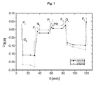
Figure 7 shows the response of the sensory organic material according to another embodiment of the invention, in particular, the variation in the resistance of an organic sensor formed of (BEDT-TTF)2I3 and polycarbonate in a vacuum (P0), and in the presence of O2, N2 and He. -
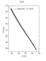
Figure 8 shows the response of the sensory organic material according to another embodiment of the invention, in particular, the variation, at ambient pressure, of the resistance with the temperature applied in an organic sensor device formed of (BET-TTF)2IxBr3-x and polycarbonate. - A mixture of 0.98 g of poly-(bisphenol-A-carbonate) (PC) and 0.02 g of bis(ethylendithio)-tetrathiafulvalene (BEDT-TTF) was prepared in 50 ml of 1.2-dichlorobenzene and heated at 80°C until the total dissolution thereof. The resulting solution was deposited on a glass surface at 130°C, allowing the solvent to evaporate, thereby obtaining a film having a thickness of 20 microns. Next, the film surface was exposed to the vapours of a dissolution saturated with iodine in methylene chloride for three minutes. This gave rise to the formation of a semiconductive superficial layer having a thickness of 1.5 microns formed by (BEDT-TTF)2I3 salt micro- and nanocrystals.
- A circular sample having a diameter of 8 mm (resistance to ambient conditions of 4.8 kOhm) of the film was cut and mounted on a glass tube with epoxy. The dependence of the resistance with pressure was measured using the four-point dc method with four platinum cables having a diameter of 20 microns (
Figure 4 ). The resistance of the film demonstrates a high piezoelectric effect (Figure 5 ). Within a pressure range of 0-100 mbar, resistance increased linearly at a speed of 45% bar-1. - A mixture of 0.98 g of poly-(bisphenol-A-carbonate) (PC) and 0.02 g of bis(ethylenthio)-tetrathiafulvalene (BET-TTF) was prepared in 50 ml of 1.2-dichlorobenzene and heated at 80°C until the total dissolution thereof. The resulting solution was deposited on a glass surface at 130°C, allowing the solvent to evaporate, thereby obtaining a film having a thickness of 25 microns.
- The surface of said film was exposed to the vapours of a dissolution saturated with iodine bromide in methylene chloride for five minutes. This gave rise to the formation of a semiconductive superficial layer having a thickness of 1.5 microns formed by (BET-TTF)2IxBr3-x salt micro- and nanocrystals.
- A circular sample having a diameter of 10 mm (resistance to ambient conditions of 4.3 kOhm) of the film was cut and mounted on a glass tube with epoxy. In order to activate the gas-sensing properties, the sensor was placed in a vacuum chamber to eliminate the possible gases or impurities that could be absorbed in the film. The dependence of the resistance with the presence of a CO2-bearing gas that contained water or methanol was measured using the four-point dc method with four platinum cables having a diameter of 20 microns (
Figure 4 ). The response of the sensor is shown inFigure 6 , where we can observe that the sensor is very sensitive and responds to the two gas mixtures in a selective manner: resistance increases significantly when the CO2 contains methanol and diminishes when it contains water. Upon producing a vacuum the initial value of the resistance is recovered. - Said film surface was exposed to the vapours of a dissolution saturated with iodine bromide in methylene chloride for six minutes. This gave rise to the formation of a semiconductive superficial layer having a thickness of 1.5 microns formed of (BET-TTF)2IxBr3-x salt micro- and nanocrystals.
- A circular sample having a diameter of 10 mm (resistance to ambient conditions of 3.0 kOhm) of the film was cut and mounted on a glass tube with epoxy. In order to activate the gas-sensing properties, the sensor was placed in a vacuum chamber to eliminate the possible gases or impurities that could be absorbed in the film. The film was exposed to O2, N2 and He gases and the electric response was measured using the four-point dc method with four platinum cables having a diameter of 20 microns. The response of the sensor device is shown in
Figure 7 . We can observe that the sensor reacts differently to the presence of these gases: in a vacuum, N2 or He atmosphere the resistance of the organic conductor increases with respect to the resistance in an O2 atmosphere. After producing the vacuum, the initial value of the resistance is recovered. - Said film surface was exposed to the vapours of a dissolution saturated with iodine bromide in methylene chloride for eight minutes. This gave rise to the formation of a semiconductive superficial layer having a thickness of 2 microns formed of (BET-TTF)2IxBr3-x salt micro- and nanocrystals.
- A circular sample having a diameter of 10 mm (resistance to ambient conditions of 2.6 kOhm) of the film was cut and mounted on a glass tube with epoxy. In order to activate the gas-sensing properties, the sensor was placed in a vacuum chamber to eliminate the possible gases or impurities that could be absorbed in the film. The film was exposed to O2, N2 and He gases and the electric response was measured using the four-point dc method with four platinum cables having a diameter of 20 microns. The response of the sensor device is shown in
Figure 7 . We can observe that the film is very sensitive to the gases to which it is exposed, although the response is lower than in the case of the film described in Example 2b. After producing the vacuum, the initial value of the resistance was recovered. - Said film surface was exposed to the vapours of a dissolution of 1 mg/ml of iodine bromide in methylene chloride for two minutes. This gave rise to the formation of a semiconductive superficial layer having a thickness of 1.5 microns formed of (BET-TTF)2IxBr3-x salt micro- and nanocrystals.
- A 2x1 mm2 rectangular sample of the film was cut and the dependence of the resistance with the temperature was measured using the four-point dc method with four platinum cables having a diameter of 20 microns. The resistance of the film reveals a high effect with the temperature (
Figure 8 ). Within a temperature range of 28-65°C resistance diminishes linearly at a speed of 7% °C-1. - The results (see Table 1, Table 2 and Table 3) of the trials conducted on an organic sensor device in accordance with the present invention are included below:
Table 1 N ΔP (mbar) ΔR (Ohm) ΔR/R0 (%) 1 0 0 0 2 2.5 4.5 0.09 3 5.5 10.4 0.22 4 9.0 16.2 0.34 5 12.0 24.4 0.51 6 15.4 31.3 0.65 7 19.0 38.7 0.80 8 22.0 45.5 0.95 9 25.7 54.5 1.14 10 30.7 66.9 1,39 11 37.3 82.3 1.71 12 41.0 89.9 1.87 13 44.8 104.2 2.17 14 53.8 119.9 2.50 15 61.5 134.6 2.80 16 67.7 147.1 3.06 17 75.1 161.2 3.36 18 79.5 169.2 3.51 19 84.0 179.6 3.74 20 87.7 187.9 3.91 21 90.6 194.4 4.05 22 94.0 200.4 4.18 23 97.5 208.6 4.35 24 101.3 214.9 4.48 25 93.9 207.5 4.32 26 90.0 200.6 4.18 27 86.0 193.0 4.02 28 82.2 183.5 3.82 29 77.8 176.1 3.66 30 70.1 161.4 3.36 31 52.5 123.9 2.58 32 27.0 67.7 1.41 33 20.6 54.3 1.13 34 13.0 34.3 0.71 35 0 0 0 Piezosensitivity κ = ΔR/ΔP R0; κ ≅ 45% - Said Table 1 shows the results obtained in a sensor device based on a layer of organic material (BEDT-TTF)2|3, where ΔP=P-P0 is the pressure differential between the applied pressure P and the ambient pressure P0; and where ΔR=R(P)-R0 is the resistance differential between the resistance to an applied pressure R(P) and the resistance to the ambient pressure R0.
Table 2 Gas ΔR/R0 Nitrogen -0.01 Helium -0.01 CO2 0.01 CO2+H2O -0.13 CO2+CH3OH 0.23 Oxygen -0.22 - Said Table 2 shows a summary of the results on the sensitivity of the gases of the resistance of the layer of sensor organic material to gas changes in a sensor device based on the molecular conductor (BET-TTF)2|xBr3-x, where ΔR=R(gas)-R0 is the resistance differential between the resistance of layer i) in the presence of a gas and the resistance R0 of the layer i) in a vacuum (R0=18 kOhm).
Table 3 N T R(T) ΔR ΔR/R0 (°C) (kΩ) (kΩ) (%) 1 28.000 51.164 0 0 2 29.276 50.681 -0.483 -0.94 3 30.552 50.083 -1.081 -2.11 4 31.828 49.559 -1.605 -3.14 5 33.103 49.059 -2.105 -4.11 6 34.379 48.587 -2.577 -5.04 7 35.655 48.111 -3.053 -5.97 8 36.931 47.607 -3.557 -6.95 9 38.207 47.119 -4.045 -7.91 10 39.483 46.665 -4.499 -8.79 11 40.759 46.206 -4.958 -9.69 12 42.034 45.747 -5.417 -10.59 13 43.310 45.287 -5.877 -11.49 14 44.586 44.848 -6.316 -12.34 15 45.862 44.401 -6.763 -13.22 16 47.138 43.980 -7.184 -14.04 17 48.414 43.547 -7.617 -14.89 18 49.690 43.106 -8.058 -15.75 19 50.966 42.660 -8.504 -16.62 20 52.241 42.212 -8.952 -17.50 21 53.517 41.826 -9.338 -18.25 22 54.793 41.379 -9.785 -19.13 23 56.069 40.938 -10.226 -19.99 24 57.345 40.551 -10.613 -20.74 25 58.621 40.118 -11.046 -21.59 26 59.897 39.691 -11.473 -22.42 27 61.172 39.258 -11.906 -23.27 28 62.448 38.788 -12.376 -24.19 29 63.724 38.297 -12.867 -25.15 30 65.000 37.820 -13.344 -26.08 - Said Table 3 shows the results obtained in a sensor device based on a layer of organic material (BET)2IxBr3-x, where ΔR = R(T) - R0 is the resistance differential between resistance at an applied temperature and resistance at ambient temperature.
Claims (18)
- Organic sensor device characterised in that it consists of:i) a layer of organic material sensitive to changes in pressure, voltage, deformation, gases and/or temperature; wherein said layer of organic material is formed of at least one salt or conductive complex including a molecule A and a dopant D, said molecule A being an electron donor or acceptor organic molecule or macromolecule capable of forming a conductive salt or complex, which without doping is not conductive, and said dopant D being a compound that is an electron acceptor or donor capable of forming a salt or conductive complex with the molecule or macromolecule A; andii) a base substrate, in close contact with said layer of organic material i), where said base substrate is inert with respect to said layer of organic material i).
- Organic sensor device, according to claim 1, characterised in that said molecule or macromolecule A will be selected from among an acene, coronene, tetrathiafulvalene or tetracyanoquinodimethane derivative.
- Organic sensor device, according to claim 2, characterised in that said molecule or macromolecule A is selected from among bis(ethylenthio)tetrathiafulvalene (BET-TTF) or bis(etylendithio)tetrathiafulvalene (BEDT-TTF).
- Organic sensor device, according to claim 1, characterised in that said dopant D is a volatile species.
- Organic sensor device, according to claim 4, characterised in that said volatile species is selected from among iodine, bromine, iodine bromide, chorine or iodine chloride.
- Organic sensor device, according to claim 1, characterised in that said salt is selected from among BEDT-TTF)2I3 and (BET-TTF)2IxBr3-x, where BET-TTF is bis(ethylenthio)tetrathiafulvalene and BEDT-TTF is bis(etylendithio)tetrathiafulvalene.
- Organic sensor device, according to claim 1, characterised in that said base substrate is inert with respect to said organic layer sensitive to changes in pressure, voltage, deformation, temperature or gases, and may be inorganic, metallic, polymeric or a three-dimensional crystal.
- Organic sensor device, according to claim 7, characterised in that said inorganic base substrate is selected from among silicium oxide or aluminum oxide.
- Organic sensor device, according to claim 7, characterised in that said base substrate is a non-conductive organic polymer.
- Organic sensor device, according to claim 9, characterised in that said base substrate is a thermoplastic polymer or elastomer.
- Organic sensor device, according to claim 10, characterised in that said base substrate is selected from among polycarbonate, polymethylmetacrilate, polyethylene or polypropylene.
- Organic sensor device, according to any of the preceding claims, characterised in that due to said layer of organic material i) being of (BEDT-TTF)2I3, said device is susceptible of application as a pressure, voltage and/or deformation sensor.
- Organic sensor device, according to any of claims 1-11, characterised in that due to said layer of organic material i) being of (BET-TTF)2IxBr3-x, said device is susceptible of application as a gas sensor.
- Organic sensor device, according to any of claims 1-11, characterised in that, said layer of organic material i) being of (BET-TTF)2IxBr3-x, said device being susceptible of application as a temperature sensor.
- Use of the sensor device, according to claims 1 to 14, in the field of molecular electronics or plastic electronics and in the field of sensors.
- Use of the sensor device, according to claim 15, characterised in that it is used in breathing masks, in medicinal devices in general, motoring, clothing or textiles and intelligent footwear.
- Use of an organic material formed by at least one salt or conductive complex including a molecule A and a dopant D, said molecule A being an electron donor or acceptor organic molecule or macromolecule capable of forming a conductive salt or complex, which without doping is not conductive, and said dopant D being a compound that is an electron donor or acceptor capable of forming a salt or conductive complex with the molecule or macromolecule A as a sensor of changes in pressure, voltage, deformation and/or gases.
- Use of an organic material, according to claim 17, as a sensor of changes in temperature.
Applications Claiming Priority (2)
| Application Number | Priority Date | Filing Date | Title |
|---|---|---|---|
| ES200602887A ES2299392B1 (en) | 2006-11-14 | 2006-11-14 | ORGANIC SENSOR DEVICE AND ITS APPLICATIONS. |
| PCT/ES2007/070184 WO2008059095A1 (en) | 2006-11-14 | 2007-11-13 | Organic sensor device and its applications |
Publications (2)
| Publication Number | Publication Date |
|---|---|
| EP2091093A1 true EP2091093A1 (en) | 2009-08-19 |
| EP2091093A4 EP2091093A4 (en) | 2014-01-01 |
Family
ID=39363852
Family Applications (1)
| Application Number | Title | Priority Date | Filing Date |
|---|---|---|---|
| EP07848127.2A Withdrawn EP2091093A4 (en) | 2006-11-14 | 2007-11-13 | ORGANIC SENSOR AND ITS APPLICATIONS |
Country Status (7)
| Country | Link |
|---|---|
| US (1) | US8343436B2 (en) |
| EP (1) | EP2091093A4 (en) |
| JP (1) | JP2010509603A (en) |
| CN (1) | CN101669223A (en) |
| CA (1) | CA2669614A1 (en) |
| ES (1) | ES2299392B1 (en) |
| WO (1) | WO2008059095A1 (en) |
Cited By (1)
| Publication number | Priority date | Publication date | Assignee | Title |
|---|---|---|---|---|
| WO2017003552A1 (en) * | 2015-06-30 | 2017-01-05 | GM Global Technology Operations LLC | Method of determining volatile organic compounds |
Families Citing this family (7)
| Publication number | Priority date | Publication date | Assignee | Title |
|---|---|---|---|---|
| ES2330405B1 (en) * | 2008-06-06 | 2010-09-21 | Consejo Superior De Investigaciones Cientificas (Csic) (45%) | SENSOR CONTACT LENS, SYSTEM FOR NON-INVASIVE MONITORING OF INTRAOCULAR PRESSURE AND METHOD TO PUT YOUR MEASUREMENT. |
| ES2372082B1 (en) * | 2010-03-02 | 2013-01-30 | Consejo Superior De Investigaciones Científicas (Csic) | NON INVASIVE SENSOR TO DETERMINE FUNCTIONAL CHARACTERISTICS OF THE CORNEA AND DEVICE INCLUDING SUCH SENSOR. |
| GB2492549B (en) * | 2011-07-04 | 2015-08-26 | Pelsis Ltd | Deterrent Device |
| DK3003910T3 (en) * | 2013-05-28 | 2017-08-14 | Nestec Sa | COVER FOR DRINK PREPARATION |
| US10813384B2 (en) | 2017-12-29 | 2020-10-27 | Altria Client Services Llc | Electronic vaping device having formulation level indicator |
| CN110987250A (en) * | 2019-12-09 | 2020-04-10 | 武汉纺织大学 | Flexible pressure sensor with multiple stimulus response structure |
| CN111122024A (en) * | 2019-12-09 | 2020-05-08 | 武汉纺织大学 | Pressure sensor with multi-stimulus response structure |
Family Cites Families (15)
| Publication number | Priority date | Publication date | Assignee | Title |
|---|---|---|---|---|
| JPS5970515A (en) | 1982-10-14 | 1984-04-21 | Japan Vilene Co Ltd | Preparation of glass fiber reinforced phenol resin foam |
| FR2538110A1 (en) * | 1982-12-21 | 1984-06-22 | Commissariat Energie Atomique | PIEZORESISTIVE GAUGE AND METHOD FOR MANUFACTURING THE SAME |
| JPS61223526A (en) * | 1985-03-28 | 1986-10-04 | Agency Of Ind Science & Technol | High pressure measurement |
| SU1668855A1 (en) | 1989-05-29 | 1991-08-07 | Физико-Технический Институт Им.С.У.Умарова | Tensosensitive element |
| JPH04372179A (en) * | 1991-06-21 | 1992-12-25 | Sumitomo Electric Ind Ltd | Manufacture of element using organic superconductor |
| GB9116360D0 (en) | 1991-07-29 | 1991-09-11 | Neotronics Ltd | Device for sensing volatile materials |
| US5386715A (en) * | 1993-12-06 | 1995-02-07 | Motorola, Inc. | Gas vapor sensor |
| JPH11195792A (en) * | 1997-12-26 | 1999-07-21 | Kurabe Ind Co Ltd | Semiconductor type sensing element and method of manufacturing the same |
| JP2000292295A (en) * | 1999-04-05 | 2000-10-20 | Tokin Corp | Sensor for detecting the internal pressure of a sealed container |
| KR100552866B1 (en) * | 2001-08-09 | 2006-02-20 | 아사히 가세이 가부시키가이샤 | Organic semiconductor devices |
| US7037767B2 (en) * | 2003-03-24 | 2006-05-02 | Konica Minolta Holdings, Inc. | Thin-film transistor, thin-film transistor sheet and their manufacturing method |
| DE102004016155B3 (en) * | 2004-04-01 | 2006-05-24 | Infineon Technologies Ag | Force sensor with organic field effect transistors, pressure sensor based thereon, position sensor and fingerprint sensor |
| US7811433B2 (en) * | 2004-10-15 | 2010-10-12 | Giner, Inc. | Electrochemical carbon dioxide sensor |
| US7059196B1 (en) | 2004-11-22 | 2006-06-13 | Honeywell International Inc. | Disposable wireless pressure sensor |
| ES2272172B1 (en) * | 2005-07-29 | 2008-04-01 | Consejo Superior Investig. Cientificas | PROCEDURE FOR OBTAINING PATTERNS IN AN ORGANIC SUBSTRATE DRIVER AND ORGANIC NATURE MATERIAL AS OBTAINED. |
-
2006
- 2006-11-14 ES ES200602887A patent/ES2299392B1/en not_active Expired - Fee Related
-
2007
- 2007-11-13 CA CA002669614A patent/CA2669614A1/en not_active Abandoned
- 2007-11-13 CN CN200780049848A patent/CN101669223A/en active Pending
- 2007-11-13 EP EP07848127.2A patent/EP2091093A4/en not_active Withdrawn
- 2007-11-13 WO PCT/ES2007/070184 patent/WO2008059095A1/en not_active Ceased
- 2007-11-13 JP JP2009536755A patent/JP2010509603A/en active Pending
- 2007-11-13 US US12/515,009 patent/US8343436B2/en not_active Expired - Fee Related
Cited By (1)
| Publication number | Priority date | Publication date | Assignee | Title |
|---|---|---|---|---|
| WO2017003552A1 (en) * | 2015-06-30 | 2017-01-05 | GM Global Technology Operations LLC | Method of determining volatile organic compounds |
Also Published As
| Publication number | Publication date |
|---|---|
| WO2008059095A1 (en) | 2008-05-22 |
| ES2299392A1 (en) | 2008-05-16 |
| CA2669614A1 (en) | 2008-05-22 |
| US20100028209A1 (en) | 2010-02-04 |
| US8343436B2 (en) | 2013-01-01 |
| CN101669223A (en) | 2010-03-10 |
| EP2091093A4 (en) | 2014-01-01 |
| JP2010509603A (en) | 2010-03-25 |
| ES2299392B1 (en) | 2009-04-16 |
Similar Documents
| Publication | Publication Date | Title |
|---|---|---|
| US8343436B2 (en) | Organic sensor device and its applications | |
| Li et al. | Porous ionic membrane based flexible humidity sensor and its multifunctional applications | |
| US7270002B2 (en) | Humidity sensor element, device and method for manufacturing thereof | |
| Wohltjen et al. | A vapor-sensitive chemiresistor fabricated with planar microelectrodes and a Langmuir-Blodgett organic semiconductor film | |
| Wu et al. | Free‐standing and eco‐friendly polyaniline thin films for multifunctional sensing of physical and chemical stimuli | |
| Kim | Microheater-integrated single gas sensor array chip fabricated on flexible polyimide substrate | |
| Dan et al. | Dielectrophoretically assembled polymer nanowires for gas sensing | |
| Fan et al. | Vapor sensing properties of thermoplastic polyurethane multifilament covered with carbon nanotube networks | |
| Karuthedath et al. | Characterization of carbon black filled PDMS-composite membranes for sensor applications | |
| EP1923697A1 (en) | High sensitive resistive-type gas sensor and its manufacturing process comprising an organic-inorganic intercalated hydbrid sensing material | |
| Lee et al. | Humidity effects according to the type of carbon nanotubes | |
| ur Rahman et al. | Electrical and hysteric properties of organic compound-based humidity sensor and its dualistic interactive approach to H2O molecules | |
| Bruschi et al. | Gas and vapour effects on the resistance fluctuation spectra of conducting polymer thin-film resistors | |
| Nikolaeva et al. | ZnO nanowire-based flexible sensors for pressure and temperature monitoring | |
| Kang et al. | Three-dimensionally printed pressure sensor arrays from hysteresis-less stretchable piezoresistive composites | |
| Li et al. | Fabrication of a prototype humidity-sensitive capacitor via layer-by-layer self-assembling technique | |
| JPS62185102A (en) | Strain gage with thin discontinuous metallic layer | |
| Bruschi et al. | Sensing properties of polypyrrole-polytetrafluoroethylene composite thin films from granular metal-polymer precursors | |
| KR102838323B1 (en) | A large surface area, vertical device design gas sensor based on thiophene-based high-performance organic semiconductor materials | |
| US9976975B2 (en) | Method of making thin film humidity sensors | |
| JP2021067688A (en) | Highly-sensitive temperature sensor and manufacturing method for the same | |
| Neitzert et al. | Humidity sensing of an epoxy/MWCNT composite by electrical conductivity measurements | |
| Johari | Development of MEMS sensors for measurements of pressure, relative humidity, and temperature | |
| KR20230158471A (en) | Dopant complexes and electronic components | |
| KR101758454B1 (en) | Structure including the vacuum sensing unit using graphene |
Legal Events
| Date | Code | Title | Description |
|---|---|---|---|
| PUAI | Public reference made under article 153(3) epc to a published international application that has entered the european phase |
Free format text: ORIGINAL CODE: 0009012 |
|
| 17P | Request for examination filed |
Effective date: 20090529 |
|
| AK | Designated contracting states |
Kind code of ref document: A1 Designated state(s): AT BE BG CH CY CZ DE DK EE ES FI FR GB GR HU IE IS IT LI LT LU LV MC MT NL PL PT RO SE SI SK TR |
|
| DAX | Request for extension of the european patent (deleted) | ||
| A4 | Supplementary search report drawn up and despatched |
Effective date: 20131203 |
|
| RIC1 | Information provided on ipc code assigned before grant |
Ipc: G01L 1/22 20060101ALI20131127BHEP Ipc: B05D 5/12 20060101ALI20131127BHEP Ipc: H01L 51/00 20060101AFI20131127BHEP Ipc: G01N 27/12 20060101ALI20131127BHEP |
|
| STAA | Information on the status of an ep patent application or granted ep patent |
Free format text: STATUS: THE APPLICATION IS DEEMED TO BE WITHDRAWN |
|
| 18D | Application deemed to be withdrawn |
Effective date: 20140701 |