EP2090945A1 - Input components and method for recognising errors - Google Patents
Input components and method for recognising errors Download PDFInfo
- Publication number
- EP2090945A1 EP2090945A1 EP08002771A EP08002771A EP2090945A1 EP 2090945 A1 EP2090945 A1 EP 2090945A1 EP 08002771 A EP08002771 A EP 08002771A EP 08002771 A EP08002771 A EP 08002771A EP 2090945 A1 EP2090945 A1 EP 2090945A1
- Authority
- EP
- European Patent Office
- Prior art keywords
- analog
- input
- multiplexer
- digital converter
- input value
- Prior art date
- Legal status (The legal status is an assumption and is not a legal conclusion. Google has not performed a legal analysis and makes no representation as to the accuracy of the status listed.)
- Granted
Links
- 238000000034 method Methods 0.000 title claims abstract description 13
- 238000005259 measurement Methods 0.000 claims description 15
- 238000012360 testing method Methods 0.000 claims description 12
- 238000001514 detection method Methods 0.000 claims description 10
- 238000011156 evaluation Methods 0.000 description 3
- 241001136792 Alle Species 0.000 description 2
- 230000006978 adaptation Effects 0.000 description 1
- 230000002950 deficient Effects 0.000 description 1
- 238000010586 diagram Methods 0.000 description 1
- 238000013507 mapping Methods 0.000 description 1
- 239000004065 semiconductor Substances 0.000 description 1
Images
Classifications
-
- G—PHYSICS
- G05—CONTROLLING; REGULATING
- G05B—CONTROL OR REGULATING SYSTEMS IN GENERAL; FUNCTIONAL ELEMENTS OF SUCH SYSTEMS; MONITORING OR TESTING ARRANGEMENTS FOR SUCH SYSTEMS OR ELEMENTS
- G05B19/00—Programme-control systems
- G05B19/02—Programme-control systems electric
- G05B19/04—Programme control other than numerical control, i.e. in sequence controllers or logic controllers
- G05B19/042—Programme control other than numerical control, i.e. in sequence controllers or logic controllers using digital processors
- G05B19/0428—Safety, monitoring
-
- G—PHYSICS
- G05—CONTROLLING; REGULATING
- G05B—CONTROL OR REGULATING SYSTEMS IN GENERAL; FUNCTIONAL ELEMENTS OF SUCH SYSTEMS; MONITORING OR TESTING ARRANGEMENTS FOR SUCH SYSTEMS OR ELEMENTS
- G05B2219/00—Program-control systems
- G05B2219/20—Pc systems
- G05B2219/24—Pc safety
- G05B2219/24196—Plausibility check in channels for correct sequence or result
-
- G—PHYSICS
- G05—CONTROLLING; REGULATING
- G05B—CONTROL OR REGULATING SYSTEMS IN GENERAL; FUNCTIONAL ELEMENTS OF SUCH SYSTEMS; MONITORING OR TESTING ARRANGEMENTS FOR SUCH SYSTEMS OR ELEMENTS
- G05B2219/00—Program-control systems
- G05B2219/20—Pc systems
- G05B2219/25—Pc structure of the system
- G05B2219/25435—Multiplex for analog signals
Definitions
- the invention relates to an input module for acquiring analog measured values, comprising a first input channel for a first measurement signal, a second input channel for a second measurement signal, a first multiplexer, a second multiplexer, a first analog-to-digital converter, a second analog-to-digital converter , wherein each one input channel is assigned to a multiplexer and the first multiplexer is connected to the first and the second analog-to-digital converter such that the first measurement signal as the first input value at the first analog-to-digital converter and as a second input value at the second analog Digital converter is applied. Furthermore, the invention relates to a method for error detection in the operation of an input module for acquiring analog measured values.
- the object of the invention is to provide an input module which detects errors in internal errors allows. For example, the error detection of the errors caused by the multiplexers used in the input modules.
- the object is achieved in that means for forming a difference between the first input value and the second input value are arranged between the input channels and the analog-to-digital converters.
- the invention is based on the finding that within a voltage mesh, the input voltage of the analog-to-digital converter can be influenced.
- a potential applied as input to the analog-to-digital converter can be shifted.
- symmetrical conditions exist in the voltage meshes of an input module in the error-free case.
- the symmetry is disturbed in the event of a fault. This asymmetry can be evaluated and thus a fault within the input module can be determined.
- the means for forming the difference are formed as arranged between the multiplexers and the inputs of the analog-to-digital converters series resistors.
- a current flowing through the series resistor results in a voltage drop across this series resistor and thus influences the symmetry of the voltage mesh or provides a difference between the first input value and the second input value.
- the input channels are designed as voltage dividers.
- a process signal flowing across the voltage divider e.g. 4 ... 20 mA causes two equal voltage drops on the voltage divider, which consists of two equivalent resistors.
- These two equal partial voltages are conducted by means of the multiplexer via a plurality of switches and via the series resistors on the one hand as a first partial voltage to the first analog-to-digital converter and on the other as a second partial voltage to the second analog-to-digital converter. In the fault-free state, an input voltage of the same level must therefore be present at both analog-to-digital converters.
- a microcontroller is connected to the analog-to-digital converter for comparison of the input values digitized by the analog-to-digital converter.
- the microcontroller which is designed as an evaluation unit, a comparison of the digitized analog values determined by the analog-to-digital converters takes place.
- Such an evaluation unit can be designed, for example, as an ASIC or FPGA.
- the digitized analog first input value is preferably compared with the digitized analog second input value, and if the difference exceeds a determinable limit, an error is reported.
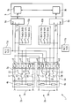
- an input module 1 for detecting an analog first measurement signal 3a and an analog second measurement signal 3b is shown in simplified form.
- the first measuring signal 3a is applied to the first input channel 2a and is divided over the first voltage divider 4a into two partial voltages of the same height.
- the switches S1 to S6 of the first multiplexer 5a are closed.
- the first partial voltage of the first voltage divider 4a is fed via the following current path to the first analog-to-digital converter 6a.
- the series resistors 8 have a value of 15 k ⁇ compared with the input resistance of the analog-to-digital converters 6a, 6b, with the analog-to-digital converters 6a, 6b having an input resistance of 80 M ⁇ . Since the ratio of the series resistors 8 to the input resistors of the analog-to-digital converters 6a, 6b is very high, the series resistors 8 do not influence the measurement result of the analog-to-digital converters 6a, 6b in the error-free case.
- the second partial voltage of the first voltage divider 4a from the first input channel 2a is also conducted via a fourth switch S4 and a fifth switch S5 of the first multiplexer 5a by means of a series resistor 8 to the second analog-to-digital converter 6b.
- the current which in this case causes the voltage for the second input value 7b at the second analog-digital converter 6b finds its way back to the first input channel 2a via a further series resistor 8 and via a sixth switch S6 of the first multiplexer 5a. Due to the redundant mapping of the first measurement signal 3a to a mutually independently operating analog-to-digital converter 6a, 6b, the availability of detection of the first measurement signal 3a already increases.
- test level A of 2.05 V
- test level B of 1.25 V
- test level C of 0.45 V
- the connection of the test levels A to C takes place in each case in conjunction with a test of a reference signal 11a or 11b of 1.25 V.
- all switching active devices can be considered, e.g. Semiconductor switches such as transistors.
Landscapes
- Physics & Mathematics (AREA)
- General Physics & Mathematics (AREA)
- Engineering & Computer Science (AREA)
- Automation & Control Theory (AREA)
- Analogue/Digital Conversion (AREA)
Abstract
Description
Die Erfindung betrifft eine Eingabebaugruppe zur Erfassung analoger Messwerte, umfassend einen ersten Eingangskanal für ein erstes Messsignal, einen zweiten Eingangskanal für ein zweites Messsignal, einen ersten Multiplexer, einen zweiten Multiplexer, einen ersten Analog-Digital-Umsetzer, einen zweiten Analog-Digital-Umsetzer, wobei je einem Eingangskanal je ein Multiplexer zugeordnet ist und der erste Multiplexer mit dem ersten und dem zweiten Analog-Digital-Umsetzer derart verschaltet ist, dass das erste Messsignal als erster Eingangswert am ersten Analog-Digital-Umsetzer und als zweiter Eingangswert am zweiten Analog-Digital-Umsetzer anliegt. Des Weiteren betrifft die Erfindung ein Verfahren zur Fehlererkennung bei dem Betrieb einer Eingabebaugruppe zur Erfassung analoger Messwerte.The invention relates to an input module for acquiring analog measured values, comprising a first input channel for a first measurement signal, a second input channel for a second measurement signal, a first multiplexer, a second multiplexer, a first analog-to-digital converter, a second analog-to-digital converter , wherein each one input channel is assigned to a multiplexer and the first multiplexer is connected to the first and the second analog-to-digital converter such that the first measurement signal as the first input value at the first analog-to-digital converter and as a second input value at the second analog Digital converter is applied. Furthermore, the invention relates to a method for error detection in the operation of an input module for acquiring analog measured values.
In der Automatisierungstechnik ist es bei sicherheitsrelevanten Prozessen erforderlich, bestimmte Prozessgrößen fehlersicher zu erfassen. Hierbei erfolgt die Erfassung von analogen Eingangssignalen, wie z.B. Druck, Temperatur, Durchfluss, Füllstand, usw., z.B. durch eine 0...20 mA- oder 4...20 mA-Schnittstelle. Bedingt durch Normen, gesetzliche Auflagen und/oder zum Schutz von Mensch und Maschine ist es erforderlich, diese als Eingangssignale vorliegenden Messwerte nahezu fehlerfrei zu erfassen.In automation technology, it is necessary for safety-relevant processes to detect certain process variables with fail-safe operation. Here, the detection of analog input signals, such as e.g. Pressure, temperature, flow, level, etc., e.g. through a 0 ... 20 mA or 4 ... 20 mA interface. Due to standards, legal requirements and / or the protection of man and machine, it is necessary to record these measured values present as input signals almost error-free.
Nach dem Stand der Technik gibt es bereits Eingabebaugruppen, welche Analogwerte redundant und fehlersicher erfassen können. Nachteilig an den nach dem Stand der Technik bekannten Eingabebaugruppen ist es, dass Fehler, welche beispielsweise bei den Multiplexern oder allgemein innerhalb der Baugruppe auftreten, nicht erkannt werden.According to the state of the art, there are already input modules which can record analog values redundantly and fail-safe. A disadvantage of the input modules known from the prior art is that errors that occur, for example, in the multiplexers or generally within the module are not recognized.
Aufgabe der Erfindung ist es, eine Eingabebaugruppe bereitzustellen, welche eine Fehleraufdeckung bei internen Fehlern ermöglicht. Beispielsweise die Fehleraufdeckung der Fehler, die durch die bei den Eingabebaugruppen eingesetzten Multiplexern hervorgerufen werden.The object of the invention is to provide an input module which detects errors in internal errors allows. For example, the error detection of the errors caused by the multiplexers used in the input modules.
Die Aufgabe wird, bezogen auf die eingangs genannte Eingabebaugruppe dadurch gelöst, dass zwischen den Eingangskanälen und den Analog-Digital-Umsetzern Mittel zur Bildung einer Differenz zwischen dem ersten Eingangswert und dem zweiten Eingangswert angeordnet sind. Der Erfindung liegt die Erkenntnis zugrunde, dass innerhalb einer Spannungsmasche die Eingangsspannung des Analog-Digital-Umsetzers beeinflusst werden kann. Durch das Einfügen von Mitteln zur Bildung einer Differenz in der Spannungsmasche, welche im Wesentlichen durch die Eingangsspannung am Analog-Digital-Umsetzer und die Eingangsspannung des Messsignals gebildet wird, lässt sich ein als Eingangswert am Analog-Digital-Umsetzer anliegendes Potenzial verschieben. Beispielsweise liegen in der Spannungsmaschen einer Eingabebaugruppe im fehlerfreien Fall symmetrische Verhältnisse vor. Hingegen wird die Symmetrie im Fehlerfall gestört. Diese Unsymmetrie lässt sich auswerten und damit ein Fehlerfall innerhalb der Eingabebaugruppe feststellen.With regard to the input module mentioned at the outset, the object is achieved in that means for forming a difference between the first input value and the second input value are arranged between the input channels and the analog-to-digital converters. The invention is based on the finding that within a voltage mesh, the input voltage of the analog-to-digital converter can be influenced. By introducing means for forming a difference in the voltage mesh, which is essentially formed by the input voltage at the analog-to-digital converter and the input voltage of the measurement signal, a potential applied as input to the analog-to-digital converter can be shifted. For example, symmetrical conditions exist in the voltage meshes of an input module in the error-free case. On the other hand, the symmetry is disturbed in the event of a fault. This asymmetry can be evaluated and thus a fault within the input module can be determined.
In einer bevorzugten Ausgestaltung der Erfindung sind die Mittel zur Bildung der Differenz als zwischen den Multiplexern und den Eingängen der Analog-Digital-Umsetzer angeordnete Längswiderstände ausgebildet. Ein über den Längswiderstand fließender Strom hat einen Spannungsabfall an diesen Längswiderstand zur Folge und beeinflusst somit die Symmetrie der Spannungsmasche bzw. sorgt er für eine Differenz zwischen dem ersten Eingangswert und dem zweiten Eingangswert. Durch die Längswiderstände, welche dem Multiplexer nachgeschaltet sind, ist es möglich, beliebige Fehler, wie z.B. Unterbrechungen, Kurzschlüsse oder Common Cause-Fehler bei den Multiplexern durch den Vergleich bzw. den Test der Analog-Digital-Umsetzer aufzudecken.In a preferred embodiment of the invention, the means for forming the difference are formed as arranged between the multiplexers and the inputs of the analog-to-digital converters series resistors. A current flowing through the series resistor results in a voltage drop across this series resistor and thus influences the symmetry of the voltage mesh or provides a difference between the first input value and the second input value. By the series resistors, which are connected downstream of the multiplexer, it is possible to detect any errors, such as interruptions, short circuits or common cause errors in the multiplexers by the comparison or the test of the analog-to-digital converter.
In einer weiteren bevorzugten Ausgestaltung sind die Eingangskanäle als Spannungsteiler ausgebildet. Ein über den Spannungsteiler fließendes Prozesssignal, z.B. 4...20 mA ruft an dem Spannungsteiler, welcher aus zwei gleichwertigen Widerständen besteht, zwei gleiche Spannungsabfälle hervor. Diese zwei gleichen Teilspannungen werden mittels des Multiplexers über mehrere Schalter und über die Längswiderstände zum Einen als eine erste Teilspannung an den ersten Analog-Digital-Umsetzer geführt und zum Anderen als eine zweite Teilspannung an den zweiten Analog-Digital-Umsetzer geführt. Im fehlerfreien Zustand muss somit an beiden Analog-Digital-Umsetzern eine Eingangsspannung gleicher Höhe anliegen.In a further preferred embodiment, the input channels are designed as voltage dividers. A process signal flowing across the voltage divider, e.g. 4 ... 20 mA causes two equal voltage drops on the voltage divider, which consists of two equivalent resistors. These two equal partial voltages are conducted by means of the multiplexer via a plurality of switches and via the series resistors on the one hand as a first partial voltage to the first analog-to-digital converter and on the other as a second partial voltage to the second analog-to-digital converter. In the fault-free state, an input voltage of the same level must therefore be present at both analog-to-digital converters.
Vorzugsweise ist zum Vergleich der durch den Analog-Digital-Umsetzer digitalisierten Eingangswerte ein Microcontroller mit dem Analog-Digital-Umsetzer verschaltet. In dem Microcontroller, welcher als eine Auswerteeinheit ausgelegt ist, findet ein Vergleich der von den Analog-Digital-Umsetzern ermittelten digitalisierten Analogwerte statt. Solch eine Auswerteeinheit kann beispielsweise als ein ASIC oder FPGA ausgestaltet sein.Preferably, a microcontroller is connected to the analog-to-digital converter for comparison of the input values digitized by the analog-to-digital converter. In the microcontroller, which is designed as an evaluation unit, a comparison of the digitized analog values determined by the analog-to-digital converters takes place. Such an evaluation unit can be designed, for example, as an ASIC or FPGA.
Weiterhin ist es vorteilhaft, wenn in der Eingabebaugruppe eine Aufschaltvorrichtung zum Aufschalten von Testpegeln an den Analog-Digital-Umsetzer vorhanden ist. Durch die Aufschaltung mehrerer verschiedener Messwerte wird die Fehleraufdeckung in einer Eingabebaugruppe durch ein weiteres erhöht.Furthermore, it is advantageous if in the input module, a Aufschaltvorrichtung for connecting test levels to the analog-to-digital converter is present. By connecting several different measured values, the fault detection in one input module is increased by another.
Verfahrensmäßig wird die Fehlererkennung bei einer Eingabebaugruppe zur Erfassung analoger Messwerte, wobei über einen ersten Eingangskanal ein erstes Messsignal mittels eines Multiplexers an den Eingang eines ersten Analog-Digital-Umsetzers als erster Eingangswert und an den Eingang eines zweiten Analog-Digital-Umsetzer als zweiten Eingangswert geschaltet wird, dadurch gelöst, dass im Fehlerfall die Eingangswerte über Mittel zur Bildung einer Differenz beeinflusst werden und diese Differenz als Fehler erkannt wird.The method of error detection in an input module for detecting analog measured values, wherein via a first input channel, a first measurement signal by means of a multiplexer to the input of a first analog-to-digital converter as a first input value and to the input of a second analog-to-digital converter as a second input value is switched off, solved in that in case of error, the input values are influenced by means for forming a difference and this difference is detected as an error.
Weitere verfahrensgemäße Vorteile sind dem Beispiel zu entnehmen.Further advantages according to the method can be found in the example.
Bevorzugt wird bei dem Verfahren der digitalisierte analoge ersten Eingangswert mit dem digitalisierten analogen zweiten Eingangswert verglichen und wenn die Differenz eine bestimmbare Grenze überschreitet ein Fehler gemeldet. Durch den Vergleich der bereits digitalisierten Werte ist es möglich, auch die fehlerfreie Funktion der Analog-Digital-Umsetzer zu betrachten.In the method, the digitized analog first input value is preferably compared with the digitized analog second input value, and if the difference exceeds a determinable limit, an error is reported. By comparing the already digitized values, it is possible to consider the error-free function of the analog-to-digital converter.
Im Folgenden wird die Erfindung anhand der Figuren näher beschrieben und erläutert. Es zeigt:
- FIG 1
- ein Blockschaltbild einer Eingabebaugruppe mit Längswiderständen und Multiplexer.
- FIG. 1
- a block diagram of an input module with series resistors and multiplexer.
Gemäß
Die zweite Teilspannung des ersten Spannungsteilers 4a vom ersten Eingangskanal 2a wird über einen vierten Schalter S4 und einen fünften Schalter S5 des ersten Multiplexers 5a ebenfalls mittels eines Längswiderstandes 8 an den zweiten Analog-Digital-Umsetzer 6b geführt. Der Strom, der hierbei am zweiten Analog-Digital-Umsetzer 6b die Spannung für den zweiten Eingangswert 7b hervorruft, findet seinen Rückweg zum ersten Eingangskanal 2a über einen weiteren Längswiderstand 8 und über einen sechsten Schalter S6 des ersten Multiplexers 5a. Durch die redundante Abbildung des ersten Messsignals 3a an jeweils einen voneinander unabhängig arbeitenden Analog-Digital-Umsetzer 6a,6b erhöht sich bereits die Verfügbarkeit der Erfassung des ersten Messsignals 3a.The second partial voltage of the
Da aber auch die Schalter S1 bis S6 der Multiplexer 5a,5b fehleranfällig sind und bisher keine Möglichkeit zur Verfügung stand, die Funktionsweise der Schalter S1 bis S6 der Multiplexer 5a,5b zu testen, wird durch die Reihenschaltung der Längswiderstände 8 nun die Möglichkeit der Fehleraufdeckung für Fehler der Multiplexer 5a,5b gegeben. Folgender Fehlerfall wäre vorstellbar:
- Während der Erfassung des ersten Messsignals 3a über den ersten Eingangskanal 2a ist der erste
Multiplexer 5a aktiv und der zweiteMultiplexer 5b inaktiv. Aktiv bedeutet hierbei, dass alle Schalter S1 bis S6 des erstenMultiplexers 5a im fehlerfreien Zustand geschlossen sind. Inaktiv bedeutet hierbei, dass alle Schalter S1 bis S6 des zweitenMultiplexers 5b im fehlerfreien Zustand geöffnet sind. Als Fehlerim zweiten Multiplexer 5b liegt nun vor, dass der erste Schalter S1 nicht mehr öffnet. Über diesen defekten Schalter S1 des zweitenMultiplexers 5b kann nun ein Ausgleichsstrom fließen. Dieser Ausgleichsstrom macht sich an dem relativ niederohmigen Längswiderstand 8 als Spannungsabfall bemerkbar. Dieser zusätzlicheSpannungsabfall am Längswiderstand 8 führt dazu, dass eine Differenz zwischen dem ersten Eingangswert 7a und dem zweiten Eingangswert 7b auftritt. Ein mit dem ersten und zweiten Analog-Digital-Umsetzer 6b verbundener Microcontroller 9 wertet die digitalisierten Analogwerte aus und vergleicht sie miteinander. Wird bei diesem Vergleich eine vorgegebene Grenze überschritten, so wird dasüber den Microcontroller 9 als Fehler gemeldet.Der Microcontroller 9 hat des Weiteren die Aufgabe, über nicht dargestellte Signalleitungen dieMultiplexer Der Microcontroller 9 weist weiterhin für die Erfassung der digitalisierten Werte einen ersten und einen zweitenMicrocontroller
- During the detection of the
first measurement signal 3a via the first input channel 2a, thefirst multiplexer 5a is active and thesecond multiplexer 5b is inactive. Active here means that all switches S1 to S6 of thefirst multiplexer 5a in error-free state are closed. Inactive here means that all switches S1 to S6 of thesecond multiplexer 5b are open in the faultless state. As an error in thesecond multiplexer 5b is now that the first switch S1 does not open. A compensating current can now flow via this defective switch S1 of thesecond multiplexer 5b. This compensating current is noticeable at the relatively low-resistance series resistor 8 as a voltage drop. This additional voltage drop across theseries resistor 8 causes a difference to occur between thefirst input value 7a and thesecond input value 7b. Amicrocontroller 9 connected to the first and second analog-to-digital converters microcontroller 9 as an error. Furthermore, themicrocontroller 9 has the task of controlling themultiplexers device microcontroller 9 furthermore has a first and asecond microcontroller
Für weitere Tests der Funktionstüchtigkeit des ersten und zweiten Multiplexers 5a,5b und der Funktionstüchtigkeit des ersten und zweiten Analog-Digital-Umsetzers 6a,6b können für den ersten Eingangskanal 2a und den zweiten Eingangskanal 2b über eine erste Aufschaltvorrichtung 10a und über eine zweite Aufschaltvorrichtung 10b je ein Testpegel A von 2,05 V, ein Testpegel B von 1,25 V und ein Testpegel C von 0,45 V an die Analog-Digital-Umsetzer 6a,6b angeschaltet werden. Aufgrund der im Fehlerfall über den Längswiderständen 8 abfallenden Spannung und der dadurch entstehenden Unsymmetrien in den unterschiedlichen Spannungsmaschen können Fehler aufgedeckt werden. Die Aufschaltung der Testpegel A bis C erfolgt jeweils in Verbindung mit einer Prüfung eines Referenzsignales 11a bzw. 11b von 1,25 V.For further tests of the operability of the first and
Durch die Integration von Längswiderständen 8 in die Messwerterfassung von Analogwerten und einer entsprechenden Anpassung einer Auswerteeinheit, hier der Microcontroller 9, kann die Fehlersicherheit, d.h. das sichere Erkennen eines Fehlers innerhalb der Eingabebaugruppe 1, erheblich erhöht werden. Des Weiteren kann bei einer Eingabebaugruppe 1 durch die Verwendung von Delta-Sigma-Umsetzern, aufgrund der spezifischen Eigenart dieser Umsetzer ein Test mit den Testpegeln A bis C in einer kürzeren Zeit erfolgen als bei dem Einsatz von herkömmlichen Umsetzern.By integrating
Als Schalter können sämtliche schaltende aktive Bauelemente betrachtet werden, z.B. Halbleiterschalter wie Transistoren.As a switch, all switching active devices can be considered, e.g. Semiconductor switches such as transistors.
Claims (9)
dadurch gekennzeichnet, dass
zwischen den Eingangskanälen (2a,2b) und den Analog-Digital-Umsetzern (6a,6b) Mittel zur Bildung einer Differenz zwischen dem ersten Eingangswert (7a) und dem zweiten Eingangswert (7b) angeordnet sind.Input module (1) for acquiring analog measured values, comprising a first input channel (2a) for a first measurement signal (3a), a second input channel (2b) for a second measurement signal (3b), a first multiplexer (5a), a second multiplexer (5b ), a first analog-to-digital converter (6a), a second analog-to-digital converter (6b), each one input channel (2a, 2b) each having a multiplexer (5a, 5b) is assigned and the first multiplexer (5a) is connected to the first and the second analog-to-digital converter (6a, 6b) in such a way that the first measuring signal (3a) acts as a first input value (7a) at the first analog-to-digital converter (6a) and as a second input value (7b). is applied to the second analog-to-digital converter (6b),
characterized in that
means for forming a difference between the first input value (7a) and the second input value (7b) are arranged between the input channels (2a, 2b) and the analog-to-digital converters (6a, 6b).
dadurch gekennzeichnet, dass
im Fehlerfall die Eingangswerte (7a,7b) über Mittel zur Bildung einer Differenz beeinflusst werden und diese Differenz als Fehler erkannt wird.A method for error detection in an input module (1) for acquiring analog measured values (3a, 3b), wherein a first input channel (2a) receives a first measuring signal (3a) by means of a multiplexer (5a) to the input of a first analog-to-digital converter (5a). 6a) is connected as a first input value (7a) and to the input of a second analog-to-digital converter (6b) as a second input value (7b),
characterized in that
in the event of an error, the input values (7a, 7b) are influenced by means for forming a difference and this difference is recognized as an error.
Priority Applications (1)
| Application Number | Priority Date | Filing Date | Title |
|---|---|---|---|
| EP20080002771 EP2090945B1 (en) | 2008-02-14 | 2008-02-14 | Input components and method for recognising errors |
Applications Claiming Priority (1)
| Application Number | Priority Date | Filing Date | Title |
|---|---|---|---|
| EP20080002771 EP2090945B1 (en) | 2008-02-14 | 2008-02-14 | Input components and method for recognising errors |
Publications (2)
| Publication Number | Publication Date |
|---|---|
| EP2090945A1 true EP2090945A1 (en) | 2009-08-19 |
| EP2090945B1 EP2090945B1 (en) | 2011-10-26 |
Family
ID=39579957
Family Applications (1)
| Application Number | Title | Priority Date | Filing Date |
|---|---|---|---|
| EP20080002771 Active EP2090945B1 (en) | 2008-02-14 | 2008-02-14 | Input components and method for recognising errors |
Country Status (1)
| Country | Link |
|---|---|
| EP (1) | EP2090945B1 (en) |
Cited By (2)
| Publication number | Priority date | Publication date | Assignee | Title |
|---|---|---|---|---|
| DE102013111888A1 (en) * | 2013-10-29 | 2015-04-30 | Phoenix Contact Gmbh & Co. Kg | Safety device for multi-channel processing of an analog input signal |
| US10749563B1 (en) | 2019-02-15 | 2020-08-18 | Siemens Aktiengesellschaft | Analog input module |
Citations (5)
| Publication number | Priority date | Publication date | Assignee | Title |
|---|---|---|---|---|
| DE4210676A1 (en) * | 1992-04-01 | 1993-10-07 | Abb Patent Gmbh | Programmable logic controller with analogue controlled stages - has analogue input and outputs set by values determined by processor as part of correction cycle |
| US5589766A (en) * | 1995-04-06 | 1996-12-31 | General Electric Company | Field-testable integrated circuit and method of testing |
| EP1282859B1 (en) | 2000-05-18 | 2003-10-15 | Siemens Aktiengesellschaft | Peripheral component with high error protection for memory programmable command apparatuses |
| US20040078715A1 (en) | 2000-05-18 | 2004-04-22 | Vaeth Joachim | Peripheral component with high error protection for stored programmable controls |
| WO2005083535A1 (en) * | 2004-03-01 | 2005-09-09 | Siemens Aktiengesellschaft | Automation system and method for identifying and correcting connection errors |
-
2008
- 2008-02-14 EP EP20080002771 patent/EP2090945B1/en active Active
Patent Citations (5)
| Publication number | Priority date | Publication date | Assignee | Title |
|---|---|---|---|---|
| DE4210676A1 (en) * | 1992-04-01 | 1993-10-07 | Abb Patent Gmbh | Programmable logic controller with analogue controlled stages - has analogue input and outputs set by values determined by processor as part of correction cycle |
| US5589766A (en) * | 1995-04-06 | 1996-12-31 | General Electric Company | Field-testable integrated circuit and method of testing |
| EP1282859B1 (en) | 2000-05-18 | 2003-10-15 | Siemens Aktiengesellschaft | Peripheral component with high error protection for memory programmable command apparatuses |
| US20040078715A1 (en) | 2000-05-18 | 2004-04-22 | Vaeth Joachim | Peripheral component with high error protection for stored programmable controls |
| WO2005083535A1 (en) * | 2004-03-01 | 2005-09-09 | Siemens Aktiengesellschaft | Automation system and method for identifying and correcting connection errors |
Cited By (6)
| Publication number | Priority date | Publication date | Assignee | Title |
|---|---|---|---|---|
| DE102013111888A1 (en) * | 2013-10-29 | 2015-04-30 | Phoenix Contact Gmbh & Co. Kg | Safety device for multi-channel processing of an analog input signal |
| EP2869147A3 (en) * | 2013-10-29 | 2016-06-08 | PHOENIX CONTACT GmbH & Co. KG | Safety device for multiple channels processing of an analogue input signal |
| DE102013111888B4 (en) | 2013-10-29 | 2018-06-14 | Phoenix Contact Gmbh & Co. Kg | Safety device for multi-channel processing of an analog input signal |
| US10749563B1 (en) | 2019-02-15 | 2020-08-18 | Siemens Aktiengesellschaft | Analog input module |
| EP3696625A1 (en) * | 2019-02-15 | 2020-08-19 | Siemens Aktiengesellschaft | Analog installation module |
| CN111580451A (en) * | 2019-02-15 | 2020-08-25 | 西门子股份公司 | Analog input module |
Also Published As
| Publication number | Publication date |
|---|---|
| EP2090945B1 (en) | 2011-10-26 |
Similar Documents
| Publication | Publication Date | Title |
|---|---|---|
| EP3265754B1 (en) | Measuring bridge arrangement with improved error detection | |
| WO2014009207A1 (en) | Apparatus for diagnosing a circuit arrangement | |
| DE102005016127B4 (en) | sensor system | |
| EP1695055A1 (en) | Measuring device, in particular a temperature measuring transducer | |
| EP2378663B1 (en) | Secure input circuit with single channel peripheral connection for the input of a bus participant | |
| DE102008018244B3 (en) | Apparatus and method for detecting a fault in a power bridge circuit | |
| EP3612846B1 (en) | Device and power supply for a control unit and method for monitoring a power supply | |
| DE10347979A1 (en) | Diagnosable switch arrangement has potential divider and state of switch arrangement can be determined by measuring voltage between potential divider node and earth potential of potential divider | |
| DE10203148B4 (en) | Error detection method and device for a sensor network | |
| EP1134589A2 (en) | Method for detecting a faulty earth connection e.g. in a vehicle | |
| DE102007046488B4 (en) | Method and device for diagnosis in integrated power bridge circuits | |
| WO2018024838A2 (en) | Protection device with a pressure-sensitive sensor for monitoring an industrial plant | |
| EP2090945B1 (en) | Input components and method for recognising errors | |
| EP1594021B1 (en) | Circuit device and method for testing relay switching contacts of a digital output circuit | |
| EP3365784B1 (en) | Circuit assembly and method for monitoring a micro-controller based on a watchdog voltage | |
| DE102007062974B4 (en) | Signal processing device | |
| EP3200033B1 (en) | Assembly comprising at least two peripheral units with a sensor | |
| EP1538453A1 (en) | Apparatus and method for fault diagnosis on digital outputs of a control element | |
| DE102013210002A1 (en) | Method and apparatus for detecting a fault in a bridge circuit | |
| DE102021111734A1 (en) | Diagnosable circuit arrangement and method for diagnosing a circuit arrangement | |
| DE102021111771A1 (en) | Diagnosis-capable circuit arrangement, sensor device with a circuit arrangement and method for diagnosing a circuit arrangement and/or sensor device | |
| EP1423719B1 (en) | Method and device for monitoring a sensor unit | |
| EP4028783A1 (en) | Battery sensor | |
| EP3226010A1 (en) | Arrangement with at least two redundant analog input units for a measuring current | |
| EP4106200B1 (en) | Proximity switch with functional safety |
Legal Events
| Date | Code | Title | Description |
|---|---|---|---|
| PUAI | Public reference made under article 153(3) epc to a published international application that has entered the european phase |
Free format text: ORIGINAL CODE: 0009012 |
|
| AK | Designated contracting states |
Kind code of ref document: A1 Designated state(s): AT BE BG CH CY CZ DE DK EE ES FI FR GB GR HR HU IE IS IT LI LT LU LV MC MT NL NO PL PT RO SE SI SK TR |
|
| AX | Request for extension of the european patent |
Extension state: AL BA MK RS |
|
| 17P | Request for examination filed |
Effective date: 20100208 |
|
| 17Q | First examination report despatched |
Effective date: 20100303 |
|
| AKX | Designation fees paid |
Designated state(s): DE FR GB IT |
|
| GRAP | Despatch of communication of intention to grant a patent |
Free format text: ORIGINAL CODE: EPIDOSNIGR1 |
|
| GRAS | Grant fee paid |
Free format text: ORIGINAL CODE: EPIDOSNIGR3 |
|
| GRAA | (expected) grant |
Free format text: ORIGINAL CODE: 0009210 |
|
| AK | Designated contracting states |
Kind code of ref document: B1 Designated state(s): DE FR GB IT |
|
| REG | Reference to a national code |
Ref country code: GB Ref legal event code: FG4D Free format text: NOT ENGLISH |
|
| REG | Reference to a national code |
Ref country code: DE Ref legal event code: R096 Ref document number: 502008005302 Country of ref document: DE Effective date: 20111229 |
|
| PLBE | No opposition filed within time limit |
Free format text: ORIGINAL CODE: 0009261 |
|
| STAA | Information on the status of an ep patent application or granted ep patent |
Free format text: STATUS: NO OPPOSITION FILED WITHIN TIME LIMIT |
|
| 26N | No opposition filed |
Effective date: 20120727 |
|
| REG | Reference to a national code |
Ref country code: DE Ref legal event code: R097 Ref document number: 502008005302 Country of ref document: DE Effective date: 20120727 |
|
| REG | Reference to a national code |
Ref country code: FR Ref legal event code: PLFP Year of fee payment: 9 |
|
| REG | Reference to a national code |
Ref country code: FR Ref legal event code: PLFP Year of fee payment: 10 |
|
| REG | Reference to a national code |
Ref country code: FR Ref legal event code: PLFP Year of fee payment: 11 |
|
| PGFP | Annual fee paid to national office [announced via postgrant information from national office to epo] |
Ref country code: FR Payment date: 20230905 Year of fee payment: 17 |
|
| PGFP | Annual fee paid to national office [announced via postgrant information from national office to epo] |
Ref country code: DE Payment date: 20230808 Year of fee payment: 17 Ref country code: GB Payment date: 20240304 Year of fee payment: 17 |
|
| PGFP | Annual fee paid to national office [announced via postgrant information from national office to epo] |
Ref country code: IT Payment date: 20230922 Year of fee payment: 17 |