EP2090900A1 - Dual range photon detector - Google Patents
Dual range photon detector Download PDFInfo
- Publication number
- EP2090900A1 EP2090900A1 EP08101698A EP08101698A EP2090900A1 EP 2090900 A1 EP2090900 A1 EP 2090900A1 EP 08101698 A EP08101698 A EP 08101698A EP 08101698 A EP08101698 A EP 08101698A EP 2090900 A1 EP2090900 A1 EP 2090900A1
- Authority
- EP
- European Patent Office
- Prior art keywords
- sdd
- detector
- scintillator
- previous
- radiation
- Prior art date
- Legal status (The legal status is an assumption and is not a legal conclusion. Google has not performed a legal analysis and makes no representation as to the accuracy of the status listed.)
- Granted
Links
Images


Classifications
-
- G—PHYSICS
- G01—MEASURING; TESTING
- G01T—MEASUREMENT OF NUCLEAR OR X-RADIATION
- G01T1/00—Measuring X-radiation, gamma radiation, corpuscular radiation, or cosmic radiation
- G01T1/16—Measuring radiation intensity
- G01T1/20—Measuring radiation intensity with scintillation detectors
- G01T1/2006—Measuring radiation intensity with scintillation detectors using a combination of a scintillator and photodetector which measures the means radiation intensity
Definitions
- the invention is related to a dual range photon detector for detecting gamma and x-ray radiation, comprising a scintillator crystal and a semiconductor detector.
- High purity germanium (HPGe) systems are in fact distinguished by superior resolution, but size, power consumption, i.e. for cooling, and prize restrict their applicability.
- the identification performance is, consequently, controlled by the limited detector resolution, in spite of recent developments like the LaBr 3 (Ce 3+ ) scintillator and the progress made in manufacturing of Cadmium-Zinc-Telluride (CZT) detectors.
- the resolution of scintiallator crystal detectors is significantly limited when the radiation energy is below 100 keV.
- SDD Silicon Drift Detectors
- SDD's can be operated without cooling and show a good energy resolution for photon energies below 100 keV. This is known for example from P. Lechner, C. Fiorini, R. Hartmann, J. Kemmer, N. Krause, P. honegger, A. Longoni, H. Soltau, D. Stötter, R. Stötter, L. Strüder, U. Weber, "Silicon drift detectors for high count rate X-ray spectroscopy at room temperature," Nucl. Instr. Meth., vol. A 458, pp. 281-287, 2001 .
- the photons emitted from the scintillator are collected and measured with a SDD, which, therefore, is mounted at the rear side of the crystal, that is the side, being opposite to where the radiation to be measured is entering the crystal.
- the SDD is not used to detect direct hits, that is low energy gamma-radiation, but only to collect and measure the amount of light emitted by the scintillator, following an absorption of gamma-radiation.
- the low energy gamma or x-ray photons are detected within the SDD, the higher energy photons within the scintillation crystal.
- the light emitted by the scintillator is again measured with the SDD.
- Marisaldi et al. make use of the significantly different timing properties, being necessary to distinguish between direct hits (SDD) and light emission (scintillator).
- An SDD creates a fast signal with a rise time between 50ns and 200ns.
- the CsI(T1) scintillator was chosen by Marisaldi et al not only because it is a non hygroscopic easy to handle material, but mainly because of its long de-excitation times of 680ns and 3.340ns respectively.
- the pulses are sent through two independent amplification chains with different shaping times of 500ns (fast chain) and 3.000ns (slow chain). As the ratio of the pulse heights are approximately constant for pulses of common shape, this will allow discrimination between the interactions taking place in SDD or in the scintillator.
- the main purpose of the present invention is therefore to avoid those disadvantages and to provide a dual range photon detector with an increased resolution especially at higher energies. Therefore, a new detector, being able to bypass those constraints, has been successfully identified and tested. It combines two distinct detection mechanisms in a compact, state-of-the-art solid-state detector, providing complementary information in different but overlapping energy ranges.
- a detector for measuring nuclear radiation especially gamma-radiation and x-rays, comprising a scintillator crystal with a light decay time of less than 200ns, preferably less than 100ns or even less than 50ns, in combination with a silicon drift detector (SDD) for the measurement of both direct hits of low energy radiation and the light, being emitted from the scintillator crystal, whereas the silicon drift detector is mounted between the scintillation crystal and the radiation entry window.
- SDD silicon drift detector
- the detector comprises a preamplifier, connected to the SDD, electronic devices, being capable of determining the signal rise time of the measured signals and of separating the signals on the basis of said rise time, as well as electronic devices, being capable of separately collecting the energy spectra of SDD and scintillator detection events on the basis of the different rise times.
- the detector comprises an LaBr3(Ce3+) scintillation crystal, having a light decay time in the order of 40ns.
- the preamplifier is partly integrated in the SDD.
- the energy resolution may be improved by providing means for cooling the detector. In most of the cases it is sufficient to cool down the detector for a limited time only, so that the cooling may be provided by a Peltier element. In most of the times it is sufficient to provide cooling for a time period in between 10s to 600s.
- the detector according to the invention provides means for spectrum analysis and radio-nuclide identification, either hard- or software implemented.
- the signals are sampled with a preferred sampling rate of 5 MS/s to 5000MS/s, especially preferred of 5 MS/s to 500MS/s.
- the detector provides means for digital signal processing, including means for preventing ballistic deficit.
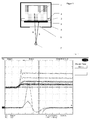
- Figure 1 shows dual-range detector, consisting of a LaBr 3 (Ce 3+ ) scintillator (1) coupled to a silicon drift detector (SDD) (2), mounted within a housing (5).
- the SDD-chip (2) is connected to the scintillation crystal (1) by an optical glue or grease (3).
- the SDD-chip (2) itself is connected to a backing (4).
- the gamma radiation, emitted from a source (7) enters the detector from SDD side through an entrance window (6).
- Low energy radiation (9) is absorbed and detected mostly within the SDD (2), whereas higher energy radiation (8) will mostly be absorbed in the scintillator crystal (1).
- the SDD (2) serves as a high-resolution X-ray and low-energy gamma detector on its own, and in parallel as a light readout device for the LaBr 3 (Ce 3+ ) scintillator (1) ensuring best possible resolution at higher energies.
- This dual-range detector based on a fast scintillator with silicon readout combines for the first time the excellent performance of an SDD as photon detector below 100 keV with the striking energy resolution of LaBr 3 (Ce 3+ ) read out by an SDD at higher energies.
- the pulse shapes due to photon absorption in silicon or scintillator differ only because of a geometrical effect, which has been employed in a detector by this invention for the first time:
- the scintillation flash illuminates a large area of the SDD; the drift paths of corresponding photoelectrons and, consequently, their drift times to the anode are very different. This causes a long slope of the anode signal composed of contributions from different SDD regions. Photon detection in the SDD is, in contrary, a local process yielding steep signals.
- One SDD module is distinguished by a perforated backing and Peltier element, which allowed exposing the SDD side of the detector configuration to gamma radiation as can be seen in figure 1 .
- FIG. 1 presents a screen shot with detector signals taken while exposing the SDD side of S-2 to a 137 Cs source.
- the screen shots of Figure 2 show preamplifier (PA, Ch1; upper part of the figure) and shaping amplifier (SPA, Ch3; lower part of the figure) output signals.
- SDD events are distinguished by rise times ⁇ 200 ns (PA, Ch1). Scintillator events exhibit longer rise times (-800 ns), even if the light decay time of the scintillator crystal is just 41ns. This reflects the drift path and drift time variance of the photo electrons.
- pulse shape discrimination allows separating the SDD and scintillator events, as demonstrated later on with the digitizing system in Figure 3 .
- Detector counts versus pulse amplitude and pulse width (PSD) measured with 137 Cs source at room temperature can be seen here.
- Pulse shape discrimination allows distinguishing scintillator and SDD events. Dominating peaks are due to 662keV gammas absorbed in the scintillator, and due to 32keV Ba-X rays absorbed in the SDD.
- the system S-2 was exposed to gamma radiation from different sources.
- the detector signals were shaped with a preamplifier from PNSensor followed by a Canberra 2020 spectroscopy amplifier, and digitized at a sampling rate of 20 MHz with a GaGe CompuScope ® .
- Simple algorithms modeling the standard analogue signal processing including PSD allowed collecting the energy spectra of scintillator and SDD events in parallel. Results are shown in Figures 4 to 8 .
- the overall detection range covers almost three decades. In practice, the lower energy limit will be controlled by absorption in the entrance window (6) of a protective housing.
- the upper limit is due to the small crystal size; but larger SDD chips and SDD arrays are available and could be combined with larger LaBr 3 (Ce 3+ ) crystals.
- the SDD spectrum covering the low-energy range up to (at least) 80keV, exhibits superior resolution if compared with a scintillator. It uncovers line structures which could never be observed with a scintillator or Cadmium Zink Telluride (CZT) detector, and which are well suited for nuclide identification and for the identification of shielding materials by analyzing corresponding X-ray fluorescence radiation.
- the SDD resolution here compensates the decreasing detection efficiency at energies >30keV (cf. Figure 4 , 133 Ba and 241 Am spectra).
- the quantum efficiency and low noise contribution of the SDD provide a better energy resolution of the scintillator spectrum if compared with a scintillator-photomultiplier combination.
- the invention is very useful for many applications. Examples are compact, handheld radionuclide identification devices, or modular, large-area imaging (standoff) radiation detection systems based on multiple dual-range detectors.
Landscapes
- Physics & Mathematics (AREA)
- Health & Medical Sciences (AREA)
- Life Sciences & Earth Sciences (AREA)
- General Physics & Mathematics (AREA)
- High Energy & Nuclear Physics (AREA)
- Molecular Biology (AREA)
- Spectroscopy & Molecular Physics (AREA)
- Measurement Of Radiation (AREA)
Abstract
Description
- The invention is related to a dual range photon detector for detecting gamma and x-ray radiation, comprising a scintillator crystal and a semiconductor detector.
- Compact, ruggedized instruments capable of detecting and classifying radioactive materials are urgently needed to uncover and to prevent illicit trafficking. The classification of sources and materials is based on nuclide identification using gamma radiation as a fingerprint.
- Most instruments exploit scintillation or CZT detectors. High purity germanium (HPGe) systems are in fact distinguished by superior resolution, but size, power consumption, i.e. for cooling, and prize restrict their applicability.
- The identification performance is, consequently, controlled by the limited detector resolution, in spite of recent developments like the LaBr3(Ce3+) scintillator and the progress made in manufacturing of Cadmium-Zinc-Telluride (CZT) detectors. In addition, the resolution of scintiallator crystal detectors is significantly limited when the radiation energy is below 100 keV.
- Semiconductor detectors, for example Silicon Drift Detectors (SDD), are also known from prior art. A SDD is mainly a rather thin Silicon disc with an anode in its center and at least one ring-like cathode in the outer part of the detector. When a photon is absorbed in the SDD, the negative charged particles move - drift - towards the center and create a pulse when the charged particles arrive at the anode.
- SDD's can be operated without cooling and show a good energy resolution for photon energies below 100 keV. This is known for example from P. Lechner, C. Fiorini, R. Hartmann, J. Kemmer, N. Krause, P. Leutenegger, A. Longoni, H. Soltau, D. Stötter, R. Stötter, L. Strüder, U. Weber, "Silicon drift detectors for high count rate X-ray spectroscopy at room temperature," Nucl. Instr. Meth., vol. A 458, pp. 281-287, 2001.
- As a consequence, combinations of scintillator crystals with silicon detectors (SD), including with silicon drift detectors (SDD), have been used for decades.
- From C. Fiorini, A. Gola, M. Zanchi, A. Longoni, P. Lechner, H. Soltau, and L. Strüder, "Gamma-Ray Spectroscopy With LaBr3:Ce Scintillator Readout by a Silicon Drift Detector," IEEE Trans. Nucl. Sci., vol. 53, no. 4, pp. 2392-2397, 2006, a gamma-ray detector is known, using LaBr3(Ce3+) as a scintillator crystal. The photons emitted from the scintillator are collected and measured with a SDD, which, therefore, is mounted at the rear side of the crystal, that is the side, being opposite to where the radiation to be measured is entering the crystal. The SDD is not used to detect direct hits, that is low energy gamma-radiation, but only to collect and measure the amount of light emitted by the scintillator, following an absorption of gamma-radiation.
- If the light decay time of the scintillator is large compared with the charge collection time in the SDD, the interactions of photons or charged particles with the SDD and with the scintillator generate detector signals with different time characteristics. M. Marisaldi, C. Labanti, and H. Soltau, "A Pulse Shape Discrimination Gamma-Ray Detector Based on a Silicon Drift Chamber Coupled to a CsI(T1) Scintillator: Prospects for a 1 keV - 1 MeV Monolithic Detector," IEEE Trans. Nucl. Sci., vol. 51, no. 4, pp. 1916-1922, 2004, disclose a dual range photon dectecor, combining a CsI(T1) scintillation crystal having a large light decay time with a silicon drift chamber or SDD with a much faster charge collection time.
- The low energy gamma or x-ray photons are detected within the SDD, the higher energy photons within the scintillation crystal. The light emitted by the scintillator is again measured with the SDD.
- In order to distinguish between the direct (low energy) hits in the SDD and the light emission from the scintillator, Marisaldi et al. make use of the significantly different timing properties, being necessary to distinguish between direct hits (SDD) and light emission (scintillator). An SDD creates a fast signal with a rise time between 50ns and 200ns. The CsI(T1) scintillator was chosen by Marisaldi et al not only because it is a non hygroscopic easy to handle material, but mainly because of its long de-excitation times of 680ns and 3.340ns respectively. According to this disclosure, the pulses are sent through two independent amplification chains with different shaping times of 500ns (fast chain) and 3.000ns (slow chain). As the ratio of the pulse heights are approximately constant for pulses of common shape, this will allow discrimination between the interactions taking place in SDD or in the scintillator.
- One of the main disadvantages of such a system is the need for a scintillation crystal like CsI(T1) with a light decay time, being substantially higher than the signal rise time of the SDD. Scintillation crystals with a short light decay time, coming down into the order of the signal rise time of the SDD cannot be used as the shaping time difference of the slow and the fast amplification channel would not be sufficient to allow for a comparable discrimination. As the light decay time of the scintillator does have an impact to the underlying noise and its energy resolution, the overall resolution of a detector as proposed by Marisaldi et al is limited.
- The main purpose of the present invention is therefore to avoid those disadvantages and to provide a dual range photon detector with an increased resolution especially at higher energies. Therefore, a new detector, being able to bypass those constraints, has been successfully identified and tested. It combines two distinct detection mechanisms in a compact, state-of-the-art solid-state detector, providing complementary information in different but overlapping energy ranges.
- More specifically, this problem is solved by providing a detector for measuring nuclear radiation, especially gamma-radiation and x-rays, comprising a scintillator crystal with a light decay time of less than 200ns, preferably less than 100ns or even less than 50ns, in combination with a silicon drift detector (SDD) for the measurement of both direct hits of low energy radiation and the light, being emitted from the scintillator crystal, whereas the silicon drift detector is mounted between the scintillation crystal and the radiation entry window. In addition, the detector comprises a preamplifier, connected to the SDD, electronic devices, being capable of determining the signal rise time of the measured signals and of separating the signals on the basis of said rise time, as well as electronic devices, being capable of separately collecting the energy spectra of SDD and scintillator detection events on the basis of the different rise times.
- In a preferred embodiment, the detector comprises an LaBr3(Ce3+) scintillation crystal, having a light decay time in the order of 40ns.
- It is an advantage if the preamplifier is partly integrated in the SDD. The energy resolution may be improved by providing means for cooling the detector. In most of the cases it is sufficient to cool down the detector for a limited time only, so that the cooling may be provided by a Peltier element. In most of the times it is sufficient to provide cooling for a time period in between 10s to 600s.
- It is a further advantage if the detector according to the invention provides means for spectrum analysis and radio-nuclide identification, either hard- or software implemented. The signals are sampled with a preferred sampling rate of 5 MS/s to 5000MS/s, especially preferred of 5 MS/s to 500MS/s.
- It is an advantage also if the detector provides means for digital signal processing, including means for preventing ballistic deficit.
- A specific embodiment of the invention is discussed in the following, using
figures 1 to 8 : - Figure 1
- shows the principal setup of the inventive detector,
- Figure 2
- shows measured preamplifier and shaping amplifier output signals, whereas
- Figure 3
- shows a three dimensional detector count spectrum, showing the effect of the achieved pulse shape discrimination.
- Figures 4 to 8
- show measured energy spectra of scintillator and SDD events for a set of radiaoactive sources at room temperature.
-
Figure 1 shows dual-range detector, consisting of a LaBr3(Ce3+) scintillator (1) coupled to a silicon drift detector (SDD) (2), mounted within a housing (5). The SDD-chip (2) is connected to the scintillation crystal (1) by an optical glue or grease (3). The SDD-chip (2) itself is connected to a backing (4). The gamma radiation, emitted from a source (7) enters the detector from SDD side through an entrance window (6). Low energy radiation (9) is absorbed and detected mostly within the SDD (2), whereas higher energy radiation (8) will mostly be absorbed in the scintillator crystal (1). The SDD (2) serves as a high-resolution X-ray and low-energy gamma detector on its own, and in parallel as a light readout device for the LaBr3(Ce3+) scintillator (1) ensuring best possible resolution at higher energies. - This dual-range detector based on a fast scintillator with silicon readout combines for the first time the excellent performance of an SDD as photon detector below 100 keV with the striking energy resolution of LaBr3(Ce3+) read out by an SDD at higher energies. Here, the pulse shapes due to photon absorption in silicon or scintillator differ only because of a geometrical effect, which has been employed in a detector by this invention for the first time: The scintillation flash illuminates a large area of the SDD; the drift paths of corresponding photoelectrons and, consequently, their drift times to the anode are very different. This causes a long slope of the anode signal composed of contributions from different SDD regions. Photon detection in the SDD is, in contrary, a local process yielding steep signals.
- Two experimental detection systems were mounted and have been tested in order to investigate prospects of such an arrangement. The SDD modules of type SDD-30-138, with an optical coating suitable for λ=380nm, were purchased from PNSensor. Both modules comprise an SDD chip mounted on a ceramics backing with Peltier cooling element in a compact housing. Encapsulated 6mm×6mm LaBr3(Ce3+) (BrilLanCe®380) crystals were purchased from Saint Gobain Crystals. The scintillators (1) were fixed with optical grease (3) on the rear contact sides of the 30mm2 SDD chips (2). One SDD module is distinguished by a perforated backing and Peltier element, which allowed exposing the SDD side of the detector configuration to gamma radiation as can be seen in
figure 1 . - All data presented in the following figures were taken at room temperature without using the Peltier element, with the SDD operated at 23-28°C.
- The two LaBr3(Ce3+)-SDD systems, S-1 and S-2, are distinguished by an energy resolution of 2.7% and 2.9% at 662 keV, respectively, while the resolution measured with the same crystals combined with common photomultiplier tubes (PMT) was only ∼3.5%. The quantum efficiency of both systems was measured and consistently found to be about 55%.
Figure 2 presents a screen shot with detector signals taken while exposing the SDD side of S-2 to a 137Cs source. The screen shots ofFigure 2 show preamplifier (PA, Ch1; upper part of the figure) and shaping amplifier (SPA, Ch3; lower part of the figure) output signals. SDD events are distinguished by rise times < 200 ns (PA, Ch1). Scintillator events exhibit longer rise times (-800 ns), even if the light decay time of the scintillator crystal is just 41ns. This reflects the drift path and drift time variance of the photo electrons. - It is evident that pulse shape discrimination (PSD) allows separating the SDD and scintillator events, as demonstrated later on with the digitizing system in
Figure 3 . Detector counts versus pulse amplitude and pulse width (PSD) measured with 137Cs source at room temperature can be seen here. Pulse shape discrimination allows distinguishing scintillator and SDD events. Dominating peaks are due to 662keV gammas absorbed in the scintillator, and due to 32keV Ba-X rays absorbed in the SDD. - In order to fathom the benefit of such dual-range detectors for nuclide identification, the system S-2 was exposed to gamma radiation from different sources. The detector signals were shaped with a preamplifier from PNSensor followed by a Canberra 2020 spectroscopy amplifier, and digitized at a sampling rate of 20 MHz with a GaGe CompuScope®. Simple algorithms modeling the standard analogue signal processing including PSD allowed collecting the energy spectra of scintillator and SDD events in parallel. Results are shown in
Figures 4 to 8 . - There, energy spectra of scintillator and SDD events, separated by PSD, as measured for a set of radioactive sources at room temperature are presented.
Figure 4 shows a measurement with 109Cd as a radioactive source,Figure 5 with 241Am,Figure 6 with 137Cs,Figure 7 with 133Ba andFigure 8 with 152Eu. The dual-range detector according to the invention is gathering complementary information in different energy ranges with the two detection mechanisms combined in a monolithic device. An 8keV XRF line due to the copper block (4) is present with all sources. This demonstrates that the invention is capable of detecting shielding material surrounding a radioactive source, which is important for classifying suspicious materials and for estimating absolute activities of sources. - The overall detection range covers almost three decades. In practice, the lower energy limit will be controlled by absorption in the entrance window (6) of a protective housing. The upper limit is due to the small crystal size; but larger SDD chips and SDD arrays are available and could be combined with larger LaBr3(Ce3+) crystals.
- The SDD spectrum, covering the low-energy range up to (at least) 80keV, exhibits superior resolution if compared with a scintillator. It uncovers line structures which could never be observed with a scintillator or Cadmium Zink Telluride (CZT) detector, and which are well suited for nuclide identification and for the identification of shielding materials by analyzing corresponding X-ray fluorescence radiation. The SDD resolution here compensates the decreasing detection efficiency at energies >30keV (cf.
Figure 4 , 133Ba and 241Am spectra). - At the high energy end, the quantum efficiency and low noise contribution of the SDD provide a better energy resolution of the scintillator spectrum if compared with a scintillator-photomultiplier combination.
- In practical applications one has to consider that the electron drift times, ranging up to some hundred nanoseconds, are influenced by the device temperature. Cooling decreases the charge carrier mobility, which is reflected in a larger maximum drift time (from the edge of the SDD to the anode). In case of scintillator events this results in a larger signal rise time. This means a temperature dependent ballistic deficit if analogue shaping with the optimum shaping time around 1 µs is applied. Digital signal processing with appropriate algorithms preventing a ballistic deficit is therefore strongly recommended.
- The invention is very useful for many applications. Examples are compact, handheld radionuclide identification devices, or modular, large-area imaging (standoff) radiation detection systems based on multiple dual-range detectors.
Claims (10)
- Detector for measuring nuclear radiation, especially gamma-radiation, comprising- a scintillator crystal with a light decay time of less than 100ns,- a silicon drift detector (SDD) for the measurement of both direct hits of low energy radiation and the light, being emitted from the scintillator crystal,- the silicon drift detector being mounted between the scintillation crystal and the radiation entry window,- a preamplifier, connected to the SDD,- electronic devices, being capable of determining the signal rise time of the measured signals and of separating the signals on the basis of said rise time,- electronic devices, being capable of separately collecting the energy spectra of SDD and scintillator detection events on the basis of the different rise times.
- Detector according to claim 1, characterized in that the scintillator crystal used has a light decay time of less than 50ns.
- Detector according to the previous claim, characterized in that the scintillator crystal comprises LaBr3(Ce3+).
- Detector according to one of the previous claims, characterized in that the preamplifier is partly integrated in the SDD.
- Detector according to one of the previous claims, comprising means for cooling the detector.
- Detector according to the previous claim, comprising a Peltier cooling element for providing a temporary temperature drop at the detector.
- Detector according to the previous claim, characterized in that the cooling element is selected so that it is able to provide cooling for a time period in between 10s to 600s.
- Detector according to one of the previous claims, comprising means for spectrum analysis and radio-nuclide identification.
- Detector according to one of the previous claims, comprising means for digital sampling of the signals with sampling rates of 5 MS/s to 5000MS/s, preferably of 5 MS/s to 500MS/s.
- Detector according to the previous claim, comprising means for digital signal processing, including means for preventing ballistic deficit.
Priority Applications (3)
| Application Number | Priority Date | Filing Date | Title |
|---|---|---|---|
| EP08101698A EP2090900B1 (en) | 2008-02-15 | 2008-02-15 | Dual range photon detector |
| PCT/EP2009/001057 WO2009100941A2 (en) | 2008-02-15 | 2009-02-16 | Dual-range photon detector |
| US12/674,932 US8212221B2 (en) | 2008-02-15 | 2009-02-16 | Dual-range photon detector |
Applications Claiming Priority (1)
| Application Number | Priority Date | Filing Date | Title |
|---|---|---|---|
| EP08101698A EP2090900B1 (en) | 2008-02-15 | 2008-02-15 | Dual range photon detector |
Publications (2)
| Publication Number | Publication Date |
|---|---|
| EP2090900A1 true EP2090900A1 (en) | 2009-08-19 |
| EP2090900B1 EP2090900B1 (en) | 2012-05-16 |
Family
ID=39870610
Family Applications (1)
| Application Number | Title | Priority Date | Filing Date |
|---|---|---|---|
| EP08101698A Not-in-force EP2090900B1 (en) | 2008-02-15 | 2008-02-15 | Dual range photon detector |
Country Status (3)
| Country | Link |
|---|---|
| US (1) | US8212221B2 (en) |
| EP (1) | EP2090900B1 (en) |
| WO (1) | WO2009100941A2 (en) |
Families Citing this family (7)
| Publication number | Priority date | Publication date | Assignee | Title |
|---|---|---|---|---|
| US8575750B1 (en) * | 2010-08-12 | 2013-11-05 | Yongdong Zhou | Semiconductor detector element configuration for very high efficiency gamma-ray detection |
| US20130187051A1 (en) * | 2011-10-06 | 2013-07-25 | Massachusetts Institute Of Technology | Frequency multiplexed superconducting nanowire photon detectors |
| RU2594991C1 (en) * | 2015-07-06 | 2016-08-20 | Федеральное государственное автономное образовательное учреждение высшего профессионального образования "Уральский федеральный университет имени первого Президента России Б.Н. Ельцина" | Detector of charged particles with thin scintillator |
| CN210442511U (en) | 2015-11-13 | 2020-05-01 | 菲力尔探测公司 | Dose rate measurement system |
| WO2017083114A1 (en) | 2015-11-13 | 2017-05-18 | Flir Detection, Inc. | Radiation detector module systems and methods |
| CN110044938A (en) * | 2019-06-05 | 2019-07-23 | 成都理工大学 | A kind of uranium concentration measuring device of spentnuclear fuel extract liquor |
| CN113835114B (en) * | 2021-08-25 | 2024-04-26 | 吉林大学 | A compact high energy gamma ray anticoincidence stack detector |
Citations (1)
| Publication number | Priority date | Publication date | Assignee | Title |
|---|---|---|---|---|
| WO2000028351A1 (en) * | 1998-11-09 | 2000-05-18 | Iwanczyk Jan S | Gamma-ray detector employing scintillators coupled to semiconductor drift photodetectors |
Family Cites Families (2)
| Publication number | Priority date | Publication date | Assignee | Title |
|---|---|---|---|---|
| US5684850A (en) * | 1995-08-14 | 1997-11-04 | William K. Warburton | Method and apparatus for digitally based high speed x-ray spectrometer |
| US5773829A (en) * | 1996-11-05 | 1998-06-30 | Iwanczyk; Jan S. | Radiation imaging detector |
-
2008
- 2008-02-15 EP EP08101698A patent/EP2090900B1/en not_active Not-in-force
-
2009
- 2009-02-16 WO PCT/EP2009/001057 patent/WO2009100941A2/en not_active Ceased
- 2009-02-16 US US12/674,932 patent/US8212221B2/en not_active Expired - Fee Related
Patent Citations (1)
| Publication number | Priority date | Publication date | Assignee | Title |
|---|---|---|---|---|
| WO2000028351A1 (en) * | 1998-11-09 | 2000-05-18 | Iwanczyk Jan S | Gamma-ray detector employing scintillators coupled to semiconductor drift photodetectors |
Non-Patent Citations (7)
| Title |
|---|
| C. FIORINI ET AL.: "Gamma-Ray Spectroscopy With LaBr3:Ce Scintillator Readout by a Silicon Drift Detector", IEEE TRANS. NUCL. SCI., vol. 53, no. 4, 2006, pages 2392 - 2397 |
| FIORINI C ET AL: "A Small Prototype of LSO-SDD Anger Camera", 1 August 2004, IEEE TRANSACTIONS ON NUCLEAR SCIENCE, IEEE SERVICE CENTER, NEW YORK, NY, US, PAGE(S) 1625 - 1630, ISSN: 0018-9499, XP011116235 * |
| FIORINI C ET AL: "Gamma-Ray Spectroscopy with LaBr3:Ce Scintillator Readout by a Silicon Drift Detector", NUCLEAR SCIENCE SYMPOSIUM CONFERENCE RECORD, 2005 IEEE WYNDHAM EL CONQUISTADOR RESORT, PUERTO RICO OCTOBER 23 - 29, 2005, PISCATAWAY, NJ, USA,IEEE, vol. 1, 23 October 2005 (2005-10-23), pages 230 - 234, XP010895579, ISBN: 978-0-7803-9221-2 * |
| FIORINI ET AL: "A large-area monolithic array of silicon drift detectors for medical imaging", NUCLEAR INSTRUMENTS & METHODS IN PHYSICS RESEARCH, SECTION - A:ACCELERATORS, SPECTROMETERS, DETECTORS AND ASSOCIATED EQUIPMENT, ELSEVIER, AMSTERDAM, NL, vol. 568, no. 1, 8 November 2006 (2006-11-08), pages 96 - 100, XP005753085, ISSN: 0168-9002 * |
| LABANTI C ET AL: "A Pulse Shape Discrimination Gamma-Ray Detector Based on a Silicon Drift Chamber Coupled to a CsI(Tl) Scintillator: Prospects for a 1 keV-1 MeV Monolithic Detector", IEEE TRANSACTIONS ON NUCLEAR SCIENCE, IEEE SERVICE CENTER, NEW YORK, NY, US, vol. 51, no. 4, 1 August 2004 (2004-08-01), pages 1916 - 1922, XP011116473, ISSN: 0018-9499 * |
| M. MARISALDI; C. LABANTI; H. SOLTAU: "A Pulse Shape Discrimination Gamma-Ray Detector Based on a Silicon Drift Chamber Coupled to a CsI(Tl) Scintillator: Prospects for a 1 keV - 1 MeV Monolithic Detector", IEEE TRANS. NUCL. SCI., vol. 51, no. 4, 2004, pages 1916 - 1922, XP011116473, DOI: doi:10.1109/TNS.2004.832679 |
| P. LECHNER ET AL.: "Silicon drift detectors for high count rate X-ray spectroscopy at room temperature", NUCL. INSTR. METH., vol. A 458, 2001, pages 281 - 287, XP027324631 |
Also Published As
| Publication number | Publication date |
|---|---|
| EP2090900B1 (en) | 2012-05-16 |
| WO2009100941A2 (en) | 2009-08-20 |
| US8212221B2 (en) | 2012-07-03 |
| WO2009100941A3 (en) | 2010-04-15 |
| US20100200762A1 (en) | 2010-08-12 |
Similar Documents
| Publication | Publication Date | Title |
|---|---|---|
| US10234572B2 (en) | Multiple spatial resolution scintillation detectors | |
| Nassalski et al. | Comparative study of scintillators for PET/CT detectors | |
| CN110082368B (en) | A Positron Annihilation Lifetime Spectrometer Based on Silicon Photomultiplier (SiPM) | |
| EP2090900B1 (en) | Dual range photon detector | |
| Schlosser et al. | Expanding the detection efficiency of silicon drift detectors | |
| WO2000028351A1 (en) | Gamma-ray detector employing scintillators coupled to semiconductor drift photodetectors | |
| EP3401706A1 (en) | Method for the detection of neutrons with scintillation detectors used for gamma ray spectroscopy | |
| US11927704B2 (en) | Hybrid radiation detector | |
| US11650338B2 (en) | Scintillation detector | |
| Farsoni et al. | A system for simultaneous beta and gamma spectroscopy | |
| Pausch et al. | Demonstration of a Dual-Range Photon Detector With SDD and ${\hbox {LaBr}} _ {3}({\hbox {Ce}}^{3+}) $ Scintillator | |
| Ford et al. | Evaluation of Eu: LiCAF for neutron detection utilizing SiPMs and portable electronics | |
| Pausch et al. | Application of 6LiI (Eu) scintillators with photodiode readout for neutron counting in mixed gamma-neutron fields | |
| Heemskerk et al. | An enhanced high-resolution EMCCD-based gamma camera using SiPM side detection | |
| EP3657221A1 (en) | Scintillation detector | |
| Herbert et al. | Investigating the energy resolution of arrays of small scintillation crystals | |
| Fiorini et al. | First experimental results of a new gamma-ray detector based on a silicon drift chamber coupled to a scintillator | |
| RU2386147C1 (en) | Multilayer detector | |
| Fiorini et al. | Performances of a silicon drift chamber as fast scintillator photodetector for gamma-ray spectroscopy | |
| RU2347241C1 (en) | Detector for recording of ionising radiation | |
| Das et al. | Development of a GAGG (Ce)-based compact 3D scanning setup for assessment of active volume in γ-ray detectors | |
| Perkins et al. | ◾ Detector Design for Small Field of View (SFOV) Nuclear Cameras | |
| Syntfeld-Kazuch et al. | Performance of CsI (Na) scintillators in γ-Ray spectrometry | |
| Kaye et al. | Beta-gated gamma coincidence counting with a phoswich detector | |
| Shah et al. | Planar APD arrays for high-resolution PET |
Legal Events
| Date | Code | Title | Description |
|---|---|---|---|
| PUAI | Public reference made under article 153(3) epc to a published international application that has entered the european phase |
Free format text: ORIGINAL CODE: 0009012 |
|
| AK | Designated contracting states |
Kind code of ref document: A1 Designated state(s): AT BE BG CH CY CZ DE DK EE ES FI FR GB GR HR HU IE IS IT LI LT LU LV MC MT NL NO PL PT RO SE SI SK TR |
|
| AX | Request for extension of the european patent |
Extension state: AL BA MK RS |
|
| 17P | Request for examination filed |
Effective date: 20100118 |
|
| AKX | Designation fees paid |
Designated state(s): AT BE BG CH CY CZ DE DK EE ES FI FR GB GR HR HU IE IS IT LI LT LU LV MC MT NL NO PL PT RO SE SI SK TR |
|
| 17Q | First examination report despatched |
Effective date: 20110330 |
|
| GRAP | Despatch of communication of intention to grant a patent |
Free format text: ORIGINAL CODE: EPIDOSNIGR1 |
|
| GRAS | Grant fee paid |
Free format text: ORIGINAL CODE: EPIDOSNIGR3 |
|
| GRAA | (expected) grant |
Free format text: ORIGINAL CODE: 0009210 |
|
| RAP1 | Party data changed (applicant data changed or rights of an application transferred) |
Owner name: FLIR RADIATION GMBH |
|
| AK | Designated contracting states |
Kind code of ref document: B1 Designated state(s): AT BE BG CH CY CZ DE DK EE ES FI FR GB GR HR HU IE IS IT LI LT LU LV MC MT NL NO PL PT RO SE SI SK TR |
|
| REG | Reference to a national code |
Ref country code: GB Ref legal event code: FG4D |
|
| REG | Reference to a national code |
Ref country code: CH Ref legal event code: EP |
|
| REG | Reference to a national code |
Ref country code: AT Ref legal event code: REF Ref document number: 558341 Country of ref document: AT Kind code of ref document: T Effective date: 20120615 |
|
| REG | Reference to a national code |
Ref country code: IE Ref legal event code: FG4D |
|
| REG | Reference to a national code |
Ref country code: DE Ref legal event code: R096 Ref document number: 602008015523 Country of ref document: DE Effective date: 20120726 |
|
| REG | Reference to a national code |
Ref country code: NL Ref legal event code: VDEP Effective date: 20120516 |
|
| REG | Reference to a national code |
Ref country code: LT Ref legal event code: MG4D Effective date: 20120516 |
|
| PG25 | Lapsed in a contracting state [announced via postgrant information from national office to epo] |
Ref country code: CY Free format text: LAPSE BECAUSE OF FAILURE TO SUBMIT A TRANSLATION OF THE DESCRIPTION OR TO PAY THE FEE WITHIN THE PRESCRIBED TIME-LIMIT Effective date: 20120516 Ref country code: LT Free format text: LAPSE BECAUSE OF FAILURE TO SUBMIT A TRANSLATION OF THE DESCRIPTION OR TO PAY THE FEE WITHIN THE PRESCRIBED TIME-LIMIT Effective date: 20120516 Ref country code: IS Free format text: LAPSE BECAUSE OF FAILURE TO SUBMIT A TRANSLATION OF THE DESCRIPTION OR TO PAY THE FEE WITHIN THE PRESCRIBED TIME-LIMIT Effective date: 20120916 Ref country code: SE Free format text: LAPSE BECAUSE OF FAILURE TO SUBMIT A TRANSLATION OF THE DESCRIPTION OR TO PAY THE FEE WITHIN THE PRESCRIBED TIME-LIMIT Effective date: 20120516 Ref country code: NO Free format text: LAPSE BECAUSE OF FAILURE TO SUBMIT A TRANSLATION OF THE DESCRIPTION OR TO PAY THE FEE WITHIN THE PRESCRIBED TIME-LIMIT Effective date: 20120816 Ref country code: FI Free format text: LAPSE BECAUSE OF FAILURE TO SUBMIT A TRANSLATION OF THE DESCRIPTION OR TO PAY THE FEE WITHIN THE PRESCRIBED TIME-LIMIT Effective date: 20120516 Ref country code: PL Free format text: LAPSE BECAUSE OF FAILURE TO SUBMIT A TRANSLATION OF THE DESCRIPTION OR TO PAY THE FEE WITHIN THE PRESCRIBED TIME-LIMIT Effective date: 20120516 |
|
| REG | Reference to a national code |
Ref country code: AT Ref legal event code: MK05 Ref document number: 558341 Country of ref document: AT Kind code of ref document: T Effective date: 20120516 |
|
| PG25 | Lapsed in a contracting state [announced via postgrant information from national office to epo] |
Ref country code: GR Free format text: LAPSE BECAUSE OF FAILURE TO SUBMIT A TRANSLATION OF THE DESCRIPTION OR TO PAY THE FEE WITHIN THE PRESCRIBED TIME-LIMIT Effective date: 20120817 Ref country code: SI Free format text: LAPSE BECAUSE OF FAILURE TO SUBMIT A TRANSLATION OF THE DESCRIPTION OR TO PAY THE FEE WITHIN THE PRESCRIBED TIME-LIMIT Effective date: 20120516 Ref country code: LV Free format text: LAPSE BECAUSE OF FAILURE TO SUBMIT A TRANSLATION OF THE DESCRIPTION OR TO PAY THE FEE WITHIN THE PRESCRIBED TIME-LIMIT Effective date: 20120516 Ref country code: PT Free format text: LAPSE BECAUSE OF FAILURE TO SUBMIT A TRANSLATION OF THE DESCRIPTION OR TO PAY THE FEE WITHIN THE PRESCRIBED TIME-LIMIT Effective date: 20120917 Ref country code: HR Free format text: LAPSE BECAUSE OF FAILURE TO SUBMIT A TRANSLATION OF THE DESCRIPTION OR TO PAY THE FEE WITHIN THE PRESCRIBED TIME-LIMIT Effective date: 20120516 |
|
| PG25 | Lapsed in a contracting state [announced via postgrant information from national office to epo] |
Ref country code: BE Free format text: LAPSE BECAUSE OF FAILURE TO SUBMIT A TRANSLATION OF THE DESCRIPTION OR TO PAY THE FEE WITHIN THE PRESCRIBED TIME-LIMIT Effective date: 20120516 |
|
| PG25 | Lapsed in a contracting state [announced via postgrant information from national office to epo] |
Ref country code: SK Free format text: LAPSE BECAUSE OF FAILURE TO SUBMIT A TRANSLATION OF THE DESCRIPTION OR TO PAY THE FEE WITHIN THE PRESCRIBED TIME-LIMIT Effective date: 20120516 Ref country code: NL Free format text: LAPSE BECAUSE OF FAILURE TO SUBMIT A TRANSLATION OF THE DESCRIPTION OR TO PAY THE FEE WITHIN THE PRESCRIBED TIME-LIMIT Effective date: 20120516 Ref country code: EE Free format text: LAPSE BECAUSE OF FAILURE TO SUBMIT A TRANSLATION OF THE DESCRIPTION OR TO PAY THE FEE WITHIN THE PRESCRIBED TIME-LIMIT Effective date: 20120516 Ref country code: DK Free format text: LAPSE BECAUSE OF FAILURE TO SUBMIT A TRANSLATION OF THE DESCRIPTION OR TO PAY THE FEE WITHIN THE PRESCRIBED TIME-LIMIT Effective date: 20120516 Ref country code: RO Free format text: LAPSE BECAUSE OF FAILURE TO SUBMIT A TRANSLATION OF THE DESCRIPTION OR TO PAY THE FEE WITHIN THE PRESCRIBED TIME-LIMIT Effective date: 20120516 Ref country code: CZ Free format text: LAPSE BECAUSE OF FAILURE TO SUBMIT A TRANSLATION OF THE DESCRIPTION OR TO PAY THE FEE WITHIN THE PRESCRIBED TIME-LIMIT Effective date: 20120516 Ref country code: AT Free format text: LAPSE BECAUSE OF FAILURE TO SUBMIT A TRANSLATION OF THE DESCRIPTION OR TO PAY THE FEE WITHIN THE PRESCRIBED TIME-LIMIT Effective date: 20120516 |
|
| PLBE | No opposition filed within time limit |
Free format text: ORIGINAL CODE: 0009261 |
|
| STAA | Information on the status of an ep patent application or granted ep patent |
Free format text: STATUS: NO OPPOSITION FILED WITHIN TIME LIMIT |
|
| 26N | No opposition filed |
Effective date: 20130219 |
|
| PG25 | Lapsed in a contracting state [announced via postgrant information from national office to epo] |
Ref country code: ES Free format text: LAPSE BECAUSE OF FAILURE TO SUBMIT A TRANSLATION OF THE DESCRIPTION OR TO PAY THE FEE WITHIN THE PRESCRIBED TIME-LIMIT Effective date: 20120827 |
|
| REG | Reference to a national code |
Ref country code: DE Ref legal event code: R097 Ref document number: 602008015523 Country of ref document: DE Effective date: 20130219 |
|
| PG25 | Lapsed in a contracting state [announced via postgrant information from national office to epo] |
Ref country code: BG Free format text: LAPSE BECAUSE OF FAILURE TO SUBMIT A TRANSLATION OF THE DESCRIPTION OR TO PAY THE FEE WITHIN THE PRESCRIBED TIME-LIMIT Effective date: 20120816 |
|
| PG25 | Lapsed in a contracting state [announced via postgrant information from national office to epo] |
Ref country code: MC Free format text: LAPSE BECAUSE OF NON-PAYMENT OF DUE FEES Effective date: 20130228 |
|
| REG | Reference to a national code |
Ref country code: CH Ref legal event code: PL |
|
| PG25 | Lapsed in a contracting state [announced via postgrant information from national office to epo] |
Ref country code: LI Free format text: LAPSE BECAUSE OF NON-PAYMENT OF DUE FEES Effective date: 20130228 Ref country code: CH Free format text: LAPSE BECAUSE OF NON-PAYMENT OF DUE FEES Effective date: 20130228 |
|
| REG | Reference to a national code |
Ref country code: IE Ref legal event code: MM4A |
|
| PG25 | Lapsed in a contracting state [announced via postgrant information from national office to epo] |
Ref country code: IE Free format text: LAPSE BECAUSE OF NON-PAYMENT OF DUE FEES Effective date: 20130215 |
|
| PGFP | Annual fee paid to national office [announced via postgrant information from national office to epo] |
Ref country code: DE Payment date: 20140220 Year of fee payment: 7 |
|
| PGFP | Annual fee paid to national office [announced via postgrant information from national office to epo] |
Ref country code: FR Payment date: 20140218 Year of fee payment: 7 Ref country code: IT Payment date: 20140225 Year of fee payment: 7 |
|
| PGFP | Annual fee paid to national office [announced via postgrant information from national office to epo] |
Ref country code: GB Payment date: 20140220 Year of fee payment: 7 |
|
| PG25 | Lapsed in a contracting state [announced via postgrant information from national office to epo] |
Ref country code: MT Free format text: LAPSE BECAUSE OF FAILURE TO SUBMIT A TRANSLATION OF THE DESCRIPTION OR TO PAY THE FEE WITHIN THE PRESCRIBED TIME-LIMIT Effective date: 20120516 |
|
| PG25 | Lapsed in a contracting state [announced via postgrant information from national office to epo] |
Ref country code: TR Free format text: LAPSE BECAUSE OF FAILURE TO SUBMIT A TRANSLATION OF THE DESCRIPTION OR TO PAY THE FEE WITHIN THE PRESCRIBED TIME-LIMIT Effective date: 20120516 |
|
| PG25 | Lapsed in a contracting state [announced via postgrant information from national office to epo] |
Ref country code: HU Free format text: LAPSE BECAUSE OF FAILURE TO SUBMIT A TRANSLATION OF THE DESCRIPTION OR TO PAY THE FEE WITHIN THE PRESCRIBED TIME-LIMIT; INVALID AB INITIO Effective date: 20080215 Ref country code: LU Free format text: LAPSE BECAUSE OF NON-PAYMENT OF DUE FEES Effective date: 20130215 |
|
| REG | Reference to a national code |
Ref country code: DE Ref legal event code: R119 Ref document number: 602008015523 Country of ref document: DE |
|
| GBPC | Gb: european patent ceased through non-payment of renewal fee |
Effective date: 20150215 |
|
| REG | Reference to a national code |
Ref country code: FR Ref legal event code: ST Effective date: 20151030 |
|
| PG25 | Lapsed in a contracting state [announced via postgrant information from national office to epo] |
Ref country code: IT Free format text: LAPSE BECAUSE OF NON-PAYMENT OF DUE FEES Effective date: 20150215 |
|
| PG25 | Lapsed in a contracting state [announced via postgrant information from national office to epo] |
Ref country code: GB Free format text: LAPSE BECAUSE OF NON-PAYMENT OF DUE FEES Effective date: 20150215 Ref country code: DE Free format text: LAPSE BECAUSE OF NON-PAYMENT OF DUE FEES Effective date: 20150901 |
|
| PG25 | Lapsed in a contracting state [announced via postgrant information from national office to epo] |
Ref country code: FR Free format text: LAPSE BECAUSE OF NON-PAYMENT OF DUE FEES Effective date: 20150302 |