EP2088626A1 - Process for producing silicon carbide semiconductor device - Google Patents
Process for producing silicon carbide semiconductor device Download PDFInfo
- Publication number
- EP2088626A1 EP2088626A1 EP07792461A EP07792461A EP2088626A1 EP 2088626 A1 EP2088626 A1 EP 2088626A1 EP 07792461 A EP07792461 A EP 07792461A EP 07792461 A EP07792461 A EP 07792461A EP 2088626 A1 EP2088626 A1 EP 2088626A1
- Authority
- EP
- European Patent Office
- Prior art keywords
- silicon carbide
- trench
- conductivity type
- carbide crystal
- semiconductor device
- Prior art date
- Legal status (The legal status is an assumption and is not a legal conclusion. Google has not performed a legal analysis and makes no representation as to the accuracy of the status listed.)
- Withdrawn
Links
Images



Classifications
-
- H—ELECTRICITY
- H10—SEMICONDUCTOR DEVICES; ELECTRIC SOLID-STATE DEVICES NOT OTHERWISE PROVIDED FOR
- H10D—INORGANIC ELECTRIC SEMICONDUCTOR DEVICES
- H10D30/00—Field-effect transistors [FET]
- H10D30/60—Insulated-gate field-effect transistors [IGFET]
- H10D30/64—Double-diffused metal-oxide semiconductor [DMOS] FETs
- H10D30/66—Vertical DMOS [VDMOS] FETs
- H10D30/668—Vertical DMOS [VDMOS] FETs having trench gate electrodes, e.g. UMOS transistors
-
- H—ELECTRICITY
- H10—SEMICONDUCTOR DEVICES; ELECTRIC SOLID-STATE DEVICES NOT OTHERWISE PROVIDED FOR
- H10P—GENERIC PROCESSES OR APPARATUS FOR THE MANUFACTURE OR TREATMENT OF DEVICES COVERED BY CLASS H10
- H10P95/00—Generic processes or apparatus for manufacture or treatments not covered by the other groups of this subclass
-
- H—ELECTRICITY
- H10—SEMICONDUCTOR DEVICES; ELECTRIC SOLID-STATE DEVICES NOT OTHERWISE PROVIDED FOR
- H10D—INORGANIC ELECTRIC SEMICONDUCTOR DEVICES
- H10D12/00—Bipolar devices controlled by the field effect, e.g. insulated-gate bipolar transistors [IGBT]
- H10D12/01—Manufacture or treatment
- H10D12/031—Manufacture or treatment of IGBTs
-
- H—ELECTRICITY
- H10—SEMICONDUCTOR DEVICES; ELECTRIC SOLID-STATE DEVICES NOT OTHERWISE PROVIDED FOR
- H10D—INORGANIC ELECTRIC SEMICONDUCTOR DEVICES
- H10D48/00—Individual devices not covered by groups H10D1/00 - H10D44/00
- H10D48/30—Devices controlled by electric currents or voltages
-
- H—ELECTRICITY
- H10—SEMICONDUCTOR DEVICES; ELECTRIC SOLID-STATE DEVICES NOT OTHERWISE PROVIDED FOR
- H10D—INORGANIC ELECTRIC SEMICONDUCTOR DEVICES
- H10D62/00—Semiconductor bodies, or regions thereof, of devices having potential barriers
- H10D62/80—Semiconductor bodies, or regions thereof, of devices having potential barriers characterised by the materials
- H10D62/83—Semiconductor bodies, or regions thereof, of devices having potential barriers characterised by the materials being Group IV materials, e.g. B-doped Si or undoped Ge
- H10D62/832—Semiconductor bodies, or regions thereof, of devices having potential barriers characterised by the materials being Group IV materials, e.g. B-doped Si or undoped Ge being Group IV materials comprising two or more elements, e.g. SiGe
- H10D62/8325—Silicon carbide
-
- H—ELECTRICITY
- H10—SEMICONDUCTOR DEVICES; ELECTRIC SOLID-STATE DEVICES NOT OTHERWISE PROVIDED FOR
- H10P—GENERIC PROCESSES OR APPARATUS FOR THE MANUFACTURE OR TREATMENT OF DEVICES COVERED BY CLASS H10
- H10P10/00—Bonding of wafers, substrates or parts of devices
-
- H—ELECTRICITY
- H10—SEMICONDUCTOR DEVICES; ELECTRIC SOLID-STATE DEVICES NOT OTHERWISE PROVIDED FOR
- H10P—GENERIC PROCESSES OR APPARATUS FOR THE MANUFACTURE OR TREATMENT OF DEVICES COVERED BY CLASS H10
- H10P95/00—Generic processes or apparatus for manufacture or treatments not covered by the other groups of this subclass
- H10P95/90—Thermal treatments, e.g. annealing or sintering
-
- H—ELECTRICITY
- H10—SEMICONDUCTOR DEVICES; ELECTRIC SOLID-STATE DEVICES NOT OTHERWISE PROVIDED FOR
- H10D—INORGANIC ELECTRIC SEMICONDUCTOR DEVICES
- H10D62/00—Semiconductor bodies, or regions thereof, of devices having potential barriers
- H10D62/40—Crystalline structures
- H10D62/405—Orientations of crystalline planes
-
- H—ELECTRICITY
- H10—SEMICONDUCTOR DEVICES; ELECTRIC SOLID-STATE DEVICES NOT OTHERWISE PROVIDED FOR
- H10D—INORGANIC ELECTRIC SEMICONDUCTOR DEVICES
- H10D64/00—Electrodes of devices having potential barriers
- H10D64/20—Electrodes characterised by their shapes, relative sizes or dispositions
- H10D64/27—Electrodes not carrying the current to be rectified, amplified, oscillated or switched, e.g. gates
- H10D64/311—Gate electrodes for field-effect devices
- H10D64/411—Gate electrodes for field-effect devices for FETs
- H10D64/511—Gate electrodes for field-effect devices for FETs for IGFETs
- H10D64/512—Disposition of the gate electrodes, e.g. buried gates
- H10D64/513—Disposition of the gate electrodes, e.g. buried gates within recesses in the substrate, e.g. trench gates, groove gates or buried gates
-
- H—ELECTRICITY
- H10—SEMICONDUCTOR DEVICES; ELECTRIC SOLID-STATE DEVICES NOT OTHERWISE PROVIDED FOR
- H10D—INORGANIC ELECTRIC SEMICONDUCTOR DEVICES
- H10D64/00—Electrodes of devices having potential barriers
- H10D64/20—Electrodes characterised by their shapes, relative sizes or dispositions
- H10D64/27—Electrodes not carrying the current to be rectified, amplified, oscillated or switched, e.g. gates
- H10D64/311—Gate electrodes for field-effect devices
- H10D64/411—Gate electrodes for field-effect devices for FETs
- H10D64/511—Gate electrodes for field-effect devices for FETs for IGFETs
- H10D64/517—Gate electrodes for field-effect devices for FETs for IGFETs characterised by the conducting layers
- H10D64/519—Gate electrodes for field-effect devices for FETs for IGFETs characterised by the conducting layers characterised by their top-view geometrical layouts
Definitions
- the present invention relates to a method of manufacturing a silicon carbide semiconductor device, and more particularly to a method of manufacturing a silicon carbide semiconductor device in which mobility of carriers in a channel of the silicon carbide semiconductor device can be improved.
- Patent Document 1 Japanese Patent Laying-Open No. 9-199724
- Patent Document 2 Japanese Patent Laying-Open No. 10-247732
- this conventional trench-gate power MOSFET is formed of a semiconductor stacked substrate 4 including an n + -type silicon carbide crystal substrate 1, an n - -type silicon carbide crystal layer 2 formed on n + -type silicon carbide crystal substrate 1, a p-type silicon carbide crystal layer 3 formed on n - -type silicon carbide crystal layer 2, and an n + -type source region 5 and a p + -type region 6 formed in a surface of p-type silicon carbide crystal layer 3.
- a hexagonal silicon carbide crystal is used as a silicon carbide crystal and an upper surface (a principal surface) of semiconductor stacked substrate 4 is a carbon surface of a substantial (0001-) surface.
- a trench 7 extending from a surface of semiconductor stacked substrate 4 through n + -type source region 5 and p-type silicon carbide crystal layer 3 into n - -type silicon carbide crystal layer 2 is formed.
- This trench 7 has side surfaces 7a perpendicular to a surface of n - -type silicon carbide crystal layer 2 and a bottom surface 7b parallel to the surface of n - -type silicon carbide crystal layer 2.
- a thin film semiconductor layer 8 made from an n-type silicon carbide crystal is epitaxially grown on side surfaces 7a of trench 7, and a gate insulating film 9 is formed on a surface of thin film semiconductor layer 8.
- a gate electrode layer 10 is formed inside gate insulating film 9.
- An interlayer insulating film 11 is formed on gate electrode layer 10, and a source electrode layer 12 is formed on n + -type source region 5 and p-type silicon carbide crystal layer 3 as well as on interlayer insulating film 11.
- a drain electrode layer 13 is formed on a surface of n + -type silicon carbide crystal substrate 1 (a lower surface of semiconductor stacked substrate 4).
- the application of an electric field to gate insulating film 9 by the application of a voltage to gate electrode layer 10 causes a storage type channel to be induced at thin film semiconductor layer 8, so that a current flows between source electrode layer 12 and drain electrode layer 13.
- trench 7 is formed by RIE (Reactive Ion Etching).
- RIE Reactive Ion Etching
- trench 7 is formed by the RIE in the method disclosed in Patent Documents 1 and 2, side surfaces 7a of trench 7 are damaged in some cases at the formation of trench 7.
- an object of the present invention is to provide a method of manufacturing a silicon carbide semiconductor device having excellent properties such as low on-resistance with the improved mobility of carriers in a channel.
- the present invention is directed to a method of manufacturing a silicon carbide semiconductor device including the steps of: in a semiconductor stacked substrate including a first conductivity type silicon carbide crystal substrate made from a hexagonal silicon carbide crystal of a first conductivity type, a first conductivity type silicon carbide crystal layer made from a hexagonal silicon carbide crystal of a first conductivity type and formed on the first conductivity type silicon carbide crystal substrate, a second conductivity type silicon carbide crystal layer made from a hexagonal silicon carbide crystal of a second conductivity type and formed on the first conductivity type silicon carbide crystal layer, and a first conductivity type semiconductor region formed on a surface of the second conductivity type silicon carbide crystal layer, forming a trench extending from a surface of the semiconductor stacked substrate through the first conductivity type semiconductor region and the second conductivity type silicon carbide crystal layer into the first conductivity type silicon carbide crystal layer defined as a bottom surface; forming a silicon film in at least a part of the trench; heating the semiconductor stacked substrate having the silicon film formed to a
- the trench is formed such that side surfaces of the trench are parallel to a [11-00] direction.
- shift and/or damage of a crystal face forming the surface exposed after the heated silicon film is removed can be reduced. Therefore, it is more likely that the mobility of the carriers in the channel of the silicon carbide semiconductor device can be further improved and a silicon carbide semiconductor device having excellent properties such as low on-resistance can be fabricated.
- the trench is formed in a hexagonal shape whose interior angles are equal to one another in the surface of the semiconductor stacked substrate.
- any side surface of the trench is made equivalent in terms of the crystal engineering. Therefore, it is more likely that a silicon carbide semiconductor device having excellent properties such as low on-resistance that has more channels with the improved mobility of the carriers can be fabricated.
- a method of manufacturing a silicon carbide semiconductor device having excellent properties such as low on-resistance with the improved mobility of carriers in a channel can be provided.
- n + -type silicon carbide crystal substrate 1 n + -type silicon carbide crystal substrate, 2 n - -type silicon carbide crystal layer, 3 p-type silicon carbide crystal layer, 4 semiconductor stacked substrate, 5 n + -type source region, 6 p + -type region, 7 trench, 7a side surface, 7b bottom surface, 8 thin film semiconductor layer, 9 gate insulating film, 10 gate electrode layer, 11 interlayer insulating film, 12 source electrode layer, 13 drain electrode layer, 14 silicon film
- an n - -type silicon carbide crystal layer 2 as a first conductivity type silicon carbide crystal layer made from an n-type hexagonal silicon carbide crystal is epitaxially grown on a surface of an n + -type silicon carbide crystal substrate 1 as a first conductivity type silicon carbide crystal substrate made from the n-type hexagonal silicon carbide crystal, whose principal surface is a carbon surface of a (0001-) crystal face.
- the (0001-) crystal face indicates a crystal face that is inclined at an angle not more than ⁇ 8° with respect to the (0001-) crystal face (including a crystal face that is not inclined with respect to the (0001-) crystal face).
- the carrier concentration of n + -type silicon carbide crystal substrate 1 is higher than that of n - -type silicon carbide crystal layer 2.
- a p-type silicon carbide crystal layer 3 as a second conductivity type silicon carbide crystal layer made from a p-type hexagonal silicon carbide crystal is epitaxially grown on a surface of n - -type silicon carbide crystal layer 2.
- an n + -type source region 5 as a first conductivity type semiconductor region is formed in a part of a surface of p-type silicon carbide crystal layer 3, for example by nitrogen ion implantation or the like.
- a p + -type region 6 is formed in a portion of the surface of p-type silicon carbide crystal layer 3 where n + -type source region 5 is not formed, for example by aluminum ion implantation or the like.
- a semiconductor stacked substrate 4 is formed. It should be noted that the carrier concentration of p + -type region 6 is higher than that of p-type silicon carbide crystal layer 3.
- a trench 7 is formed by RIE representing a dry etching method, that extends through both n + -type source region 5 and p-type silicon carbide crystal layer 3 to reach n - -type silicon carbide crystal layer 2 and has a bottom surface 7b defined by the surface of n - -type silicon carbide crystal layer 2.
- RIE a dry etching method
- trench 7 in order to form trench 7 such that side surfaces 7a of the trench are parallel to the [11-00] direction, trench 7 has only to be formed such that side surfaces 7a of the trench are parallel to any one of the six directions of ⁇ 11-00>, ⁇ 101-0>, ⁇ 011-0>, ⁇ 1-100>, ⁇ 1-010>, and ⁇ 01-10>.
- being parallel to the [11-00] direction indicates being inclined at an angle not more than ⁇ 8° with respect to any one of the above-described six directions (including the case where the above-described angle is 0°).
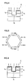
- trench 7 in the surface of semiconductor stacked substrate 4 has a hexagonal two-dimensional shape whose interior angles are equal to one another, for example as shown in a schematic plan view of Fig. 5 .
- a hexagon whose interior angles are equal to one another indicates a hexagon in which an absolute value of a difference between a maximum interior angle and a minimum interior angle is not more than 32°.
- a silicon film 14 is formed on the surface of semiconductor stacked substrate 4.
- side surfaces 7a of trench 7 are covered with silicon film 14.
- Silicon film 14 can be formed, for example, by a sputtering method.
- semiconductor stacked substrate 4 having silicon film 14 formed is heated to a temperature that is not less than the melting temperature of silicon film 14.
- a crystal face forming side surfaces 7a of trench 7 is reconfigured and side surfaces 7a of trench 7 tend to become a crystal face that is stable in terms of energy.
- the present invention from the viewpoint of the improvement in the mobility of the carriers in the channel of the silicon carbide semiconductor device, it is preferable to heat semiconductor stacked substrate 4 having silicon film 14 formed on side surfaces 7a of trench 7 at a temperature that is not less than 1300°C and not more than 1700°C. Furthermore, in the present invention, from the viewpoint of the improvement in the mobility of the carriers in the channel of the silicon carbide semiconductor device, it is preferable to heat semiconductor stacked substrate 4 having silicon film 14 formed on side surfaces 7a of trench 7, preferably at a temperature that is not less than 1300°C and not more than 1700°C for 20 minutes or longer.
- silicon film 14 formed on the surface of semiconductor stacked substrate 4 is removed.
- silicon film 14 is removed by immersion, for example, into a mixture of nitric acid and hydrogen fluoride or the like.
- a gate insulating film 9 is formed such that the surface of semiconductor stacked substrate 4, side surfaces 7a of trench 7 and bottom surface 7b of trench 7 are covered.
- a gate electrode layer 10 is formed inside gate insulating film 9 in trench 7.
- an interlayer insulating film 11 is formed on the surface of semiconductor stacked substrate 4 as well as on gate electrode layer 10.
- a source electrode layer 12 is formed on n + -type source region 5 and p + -type region 6 as well as on interlayer insulating film 11 as shown in a schematic cross-sectional view of Fig. 11 .
- a drain electrode layer 13 is formed on a back surface of semiconductor stacked substrate 4 (a back surface of n + -type silicon carbide crystal substrate 1).
- a surface exposed after the heated silicon film is removed can have a crystal face with reduced nonuniformity and/or damage as well as reduced surface level, and thus the mobility of the carriers in the channel implemented by such crystal face can be improved.
- the surface level density in the channel can be controlled to be low and a trench-gate power MOSFET having excellent properties such as low on-resistance can be fabricated.
- materials for gate electrode layer 10, source electrode layer 12 and drain electrode layer 13 are not particularly limited as long as they are conductive.
- materials for interlayer insulating film 11 are not particularly limited as long as they are insulating.
- p + -type region 6 is formed in the foregoing, p + -type region 6 may not be formed in the present invention.
- side surfaces 7a of trench 7 are formed perpendicular to the surface of semiconductor stacked substrate 4 in the foregoing, side surfaces 7a of trench 7 and the surface of semiconductor stacked substrate 4 may not necessarily form a vertical angle in the present invention.
- trench 7 may be V-shaped without having bottom surface 7b, for example as shown in a schematic cross-sectional view of Fig. 13 .
- side surface 7a of trench 7 may be curved, for example as shown in a schematic cross-sectional view of Fig. 14 .
- gate electrode layer 10 may be formed in such a shape that at least a part of an upper portion of gate electrode layer 10 is located above n + -type source region 5, for example as shown in a schematic cross-sectional view of Fig. 15 .
- a method of manufacturing a silicon carbide semiconductor device having excellent properties such as low on-resistance with the improved mobility of carriers in a channel can be provided.
Landscapes
- Electrodes Of Semiconductors (AREA)
- Insulated Gate Type Field-Effect Transistor (AREA)
Abstract
Description
- The present invention relates to a method of manufacturing a silicon carbide semiconductor device, and more particularly to a method of manufacturing a silicon carbide semiconductor device in which mobility of carriers in a channel of the silicon carbide semiconductor device can be improved.
- For example, a trench-gate power MOSFET (Metal Oxide Semiconductor Field Effect Transistor) that achieves low on-resistance and high breakdown voltage has been proposed as a conventional silicon carbide semiconductor device (see Patent Document 1 (Japanese Patent Laying-Open No.
9-199724 10-247732 - As shown in
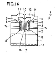
Fig. 16 , for example, this conventional trench-gate power MOSFET is formed of a semiconductor stackedsubstrate 4 including an n+-type siliconcarbide crystal substrate 1, an n--type siliconcarbide crystal layer 2 formed on n+-type siliconcarbide crystal substrate 1, a p-type siliconcarbide crystal layer 3 formed on n--type siliconcarbide crystal layer 2, and an n+-type source region 5 and a p+-type region 6 formed in a surface of p-type siliconcarbide crystal layer 3. A hexagonal silicon carbide crystal is used as a silicon carbide crystal and an upper surface (a principal surface) of semiconductor stackedsubstrate 4 is a carbon surface of a substantial (0001-) surface. - In this conventional trench-gate power MOSFET, a
trench 7 extending from a surface of semiconductor stackedsubstrate 4 through n+-type source region 5 and p-type siliconcarbide crystal layer 3 into n--type siliconcarbide crystal layer 2 is formed. Thistrench 7 hasside surfaces 7a perpendicular to a surface of n--type siliconcarbide crystal layer 2 and abottom surface 7b parallel to the surface of n--type siliconcarbide crystal layer 2. - A thin
film semiconductor layer 8 made from an n-type silicon carbide crystal is epitaxially grown onside surfaces 7a oftrench 7, and agate insulating film 9 is formed on a surface of thinfilm semiconductor layer 8. Agate electrode layer 10 is formed insidegate insulating film 9. Aninterlayer insulating film 11 is formed ongate electrode layer 10, and asource electrode layer 12 is formed on n+-type source region 5 and p-type siliconcarbide crystal layer 3 as well as on interlayerinsulating film 11. Adrain electrode layer 13 is formed on a surface of n+-type silicon carbide crystal substrate 1 (a lower surface of semiconductor stacked substrate 4). - In the conventional silicon carbide semiconductor device having such a configuration, the application of an electric field to
gate insulating film 9 by the application of a voltage togate electrode layer 10 causes a storage type channel to be induced at thinfilm semiconductor layer 8, so that a current flows betweensource electrode layer 12 anddrain electrode layer 13. - Patent Document 1: Japanese Patent Laying-Open No.
9-199724 - Patent Document 2: Japanese Patent Laying-Open No.
10-247732 - In the conventional silicon carbide semiconductor device disclosed in the above-described
Patent Documents side surfaces 7a oftrench 7 are formed in parallel to a [11-00] direction or a [112-0] direction, and thus the properties of low on-resistance and high breakdown voltage are achieved. - In a method disclosed in
Patent Documents trench 7 is formed by RIE (Reactive Ion Etching). On the other hand, even if a photolithography process is employed in the RIE, it is difficult to formside surfaces 7a oftrench 7 such that a direction thereof is completely aligned with the above-described prescribed direction. - Furthermore, since
trench 7 is formed by the RIE in the method disclosed inPatent Documents side surfaces 7a oftrench 7 are damaged in some cases at the formation oftrench 7. - Therefore, in the conventional silicon carbide semiconductor device disclosed in
Patent Documents side surfaces 7a oftrench 7 is shifted and/or damaged, and thus a crystal face of thinfilm semiconductor layer 8 formed on such a crystal face is also shifted and/or damaged in some cases. As a result, a surface level is created on the surface of thinfilm semiconductor layer 8 serving as a channel and the surface level blocks the movement of carriers. Thus, there exists a problem that the carriers in the channel do not have enough mobility and a silicon carbide semiconductor device having excellent properties such as low on-resistance cannot be provided. - Therefore, an object of the present invention is to provide a method of manufacturing a silicon carbide semiconductor device having excellent properties such as low on-resistance with the improved mobility of carriers in a channel.
- The present invention is directed to a method of manufacturing a silicon carbide semiconductor device including the steps of: in a semiconductor stacked substrate including a first conductivity type silicon carbide crystal substrate made from a hexagonal silicon carbide crystal of a first conductivity type, a first conductivity type silicon carbide crystal layer made from a hexagonal silicon carbide crystal of a first conductivity type and formed on the first conductivity type silicon carbide crystal substrate, a second conductivity type silicon carbide crystal layer made from a hexagonal silicon carbide crystal of a second conductivity type and formed on the first conductivity type silicon carbide crystal layer, and a first conductivity type semiconductor region formed on a surface of the second conductivity type silicon carbide crystal layer, forming a trench extending from a surface of the semiconductor stacked substrate through the first conductivity type semiconductor region and the second conductivity type silicon carbide crystal layer into the first conductivity type silicon carbide crystal layer defined as a bottom surface; forming a silicon film in at least a part of the trench; heating the semiconductor stacked substrate having the silicon film formed to a temperature that is not less than the melting temperature of the silicon film; removing the heated silicon film; forming a gate insulating film on a surface exposed after the silicon film is removed; and forming a gate electrode layer on a surface of the gate insulating film. By such a configuration, the mobility of carriers in a channel of the silicon carbide semiconductor device can be improved and a silicon carbide semiconductor device having excellent properties such as low on-resistance can be fabricated.
- Preferably, in the method of manufacturing a silicon carbide semiconductor device of the present invention, the trench is formed such that side surfaces of the trench are parallel to a [11-00] direction. By such a configuration, shift and/or damage of a crystal face forming the surface exposed after the heated silicon film is removed can be reduced. Therefore, it is more likely that the mobility of the carriers in the channel of the silicon carbide semiconductor device can be further improved and a silicon carbide semiconductor device having excellent properties such as low on-resistance can be fabricated.
- More preferably, in the method of manufacturing a silicon carbide semiconductor device of the present invention, the trench is formed in a hexagonal shape whose interior angles are equal to one another in the surface of the semiconductor stacked substrate. By such a configuration, any side surface of the trench is made equivalent in terms of the crystal engineering. Therefore, it is more likely that a silicon carbide semiconductor device having excellent properties such as low on-resistance that has more channels with the improved mobility of the carriers can be fabricated.
- According to the present invention, there can be provided a method of manufacturing a silicon carbide semiconductor device having excellent properties such as low on-resistance with the improved mobility of carriers in a channel.
-
-
Fig. 1 is a schematic cross-sectional view showing a part of a manufacturing process of a preferable example of a trench-gate power MOSFET as a silicon carbide semiconductor device of the present invention. -
Fig. 2 is a schematic cross-sectional view showing a part of a manufacturing process of a preferable example of a trench-gate power MOSFET as a silicon carbide semiconductor device of the present invention. -
Fig. 3 is a schematic cross-sectional view showing a part of a manufacturing process of a preferable example of a trench-gate power MOSFET as a silicon carbide semiconductor device of the present invention. -
Fig. 4 is a schematic cross-sectional view showing a part of a manufacturing process of a preferable example of a trench-gate power MOSFET as a silicon carbide semiconductor device of the present invention. -
Fig. 5 is a schematic plan view of a preferable example of a two-dimensional shape of a trench formed in the present invention. -
Fig. 6 is a schematic cross-sectional view showing a part of a manufacturing process of a preferable example of a trench-gate power MOSFET as a silicon carbide semiconductor device of the present invention. -
Fig. 7 is a schematic cross-sectional view showing a part of a manufacturing process of a preferable example of a trench-gate power MOSFET as a silicon carbide semiconductor device of the present invention. -
Fig. 8 is a schematic cross-sectional view showing a part of a manufacturing process of a preferable example of a trench-gate power MOSFET as a silicon carbide semiconductor device of the present invention. -
Fig. 9 is a schematic cross-sectional view showing a part of a manufacturing process of a preferable example of a trench-gate power MOSFET as a silicon carbide semiconductor device of the present invention. -
Fig. 10 is a schematic cross-sectional view showing a part of a manufacturing process of a preferable example of a trench-gate power MOSFET as a silicon carbide semiconductor device of the present invention. -
Fig. 11 is a schematic cross-sectional view showing a part of a manufacturing process of a preferable example of a trench-gate power MOSFET as a silicon carbide semiconductor device of the present invention. -
Fig. 12 is a schematic cross-sectional view of a preferable example of a trench-gate power MOSFET as a silicon carbide semiconductor device of the present invention. -
Fig. 13 is a schematic cross-sectional view of another preferable example of a trench-gate power MOSFET as a silicon carbide semiconductor device obtained by the present invention. -
Fig. 14 is a schematic cross-sectional view of another preferable example of a trench-gate power MOSFET as a silicon carbide semiconductor device obtained by the present invention. -
Fig. 15 is a schematic cross-sectional view of another preferable example of a trench-gate power MOSFET as a silicon carbide semiconductor device obtained by the present invention. -
Fig. 16 is a schematic cross-sectional view of a conventional trench-gate power MOSFET. - 1 n+-type silicon carbide crystal substrate, 2 n--type silicon carbide crystal layer, 3 p-type silicon carbide crystal layer, 4 semiconductor stacked substrate, 5 n+-type source region, 6 p+-type region, 7 trench, 7a side surface, 7b bottom surface, 8 thin film semiconductor layer, 9 gate insulating film, 10 gate electrode layer, 11 interlayer insulating film, 12 source electrode layer, 13 drain electrode layer, 14 silicon film
- The embodiments of the present invention will be described below. The same or corresponding parts are represented by the same reference numerals in the drawings of the present invention.
- Referring to
Figs. 1-12 , a manufacturing process of a preferable example of a trench-gate power MOSFET as a silicon carbide semiconductor device of the present invention will be described. First, as shown in a schematic cross-sectional view ofFig. 1 , an n--type siliconcarbide crystal layer 2 as a first conductivity type silicon carbide crystal layer made from an n-type hexagonal silicon carbide crystal is epitaxially grown on a surface of an n+-type siliconcarbide crystal substrate 1 as a first conductivity type silicon carbide crystal substrate made from the n-type hexagonal silicon carbide crystal, whose principal surface is a carbon surface of a (0001-) crystal face. In the present invention, the (0001-) crystal face indicates a crystal face that is inclined at an angle not more than ±8° with respect to the (0001-) crystal face (including a crystal face that is not inclined with respect to the (0001-) crystal face). The carrier concentration of n+-type siliconcarbide crystal substrate 1 is higher than that of n--type siliconcarbide crystal layer 2. - Next, as shown in a schematic cross-sectional view of
Fig. 2 , a p-type siliconcarbide crystal layer 3 as a second conductivity type silicon carbide crystal layer made from a p-type hexagonal silicon carbide crystal is epitaxially grown on a surface of n--type siliconcarbide crystal layer 2. Then, as shown in a schematic cross-sectional view ofFig. 3 , an n+-type source region 5 as a first conductivity type semiconductor region is formed in a part of a surface of p-type siliconcarbide crystal layer 3, for example by nitrogen ion implantation or the like. Furthermore, a p+-type region 6 is formed in a portion of the surface of p-type siliconcarbide crystal layer 3 where n+-type source region 5 is not formed, for example by aluminum ion implantation or the like. Thus, a semiconductor stackedsubstrate 4 is formed. It should be noted that the carrier concentration of p+-type region 6 is higher than that of p-type siliconcarbide crystal layer 3. - Then, as shown in a schematic cross-sectional view of
Fig. 4 , atrench 7 is formed by RIE representing a dry etching method, that extends through both n+-type source region 5 and p-type siliconcarbide crystal layer 3 to reach n--type siliconcarbide crystal layer 2 and has abottom surface 7b defined by the surface of n--type siliconcarbide crystal layer 2. Here, it is preferable to formtrench 7 such that side surfaces 7a of the trench are parallel to a [11-00] direction. In the present invention, in order to formtrench 7 such that side surfaces 7a of the trench are parallel to the [11-00] direction,trench 7 has only to be formed such that side surfaces 7a of the trench are parallel to any one of the six directions of <11-00>, <101-0>, <011-0>, <1-100>, <1-010>, and <01-10>. Furthermore, in the present invention, being parallel to the [11-00] direction indicates being inclined at an angle not more than ±8° with respect to any one of the above-described six directions (including the case where the above-described angle is 0°). - When
trench 7 is formed such that side surfaces 7a of the trench are parallel to the [11-00] direction,trench 7 in the surface of semiconductor stackedsubstrate 4 has a hexagonal two-dimensional shape whose interior angles are equal to one another, for example as shown in a schematic plan view ofFig. 5 . In the present invention, a hexagon whose interior angles are equal to one another indicates a hexagon in which an absolute value of a difference between a maximum interior angle and a minimum interior angle is not more than 32°. - Then, as shown in a schematic cross-sectional view of
Fig. 6 , asilicon film 14 is formed on the surface of semiconductor stackedsubstrate 4. Here, side surfaces 7a oftrench 7 are covered withsilicon film 14.Silicon film 14 can be formed, for example, by a sputtering method. - Then, semiconductor stacked
substrate 4 havingsilicon film 14 formed is heated to a temperature that is not less than the melting temperature ofsilicon film 14. Here, a crystal face formingside surfaces 7a oftrench 7 is reconfigured andside surfaces 7a oftrench 7 tend to become a crystal face that is stable in terms of energy. In other words, by performing the steps ofheating silicon film 14 formed onside surfaces 7a oftrench 7 to a temperature that is not less than the melting temperature ofsilicon film 14 and reconfiguring the crystal face formingside surfaces 7a oftrench 7, even if the crystal face is shifted and/or damaged atside surfaces 7a oftrench 7, the shift and/or damage of the crystal face can be recovered. Therefore, in the present invention, creation of a surface level due to the shift and/or damage of the crystal face in a channel can be reduced, and thus the mobility of carriers in the channel can be improved. - In the present invention, from the viewpoint of the improvement in the mobility of the carriers in the channel of the silicon carbide semiconductor device, it is preferable to heat semiconductor stacked
substrate 4 havingsilicon film 14 formed onside surfaces 7a oftrench 7 at a temperature that is not less than 1300°C and not more than 1700°C. Furthermore, in the present invention, from the viewpoint of the improvement in the mobility of the carriers in the channel of the silicon carbide semiconductor device, it is preferable to heat semiconductor stackedsubstrate 4 havingsilicon film 14 formed onside surfaces 7a oftrench 7, preferably at a temperature that is not less than 1300°C and not more than 1700°C for 20 minutes or longer. - As shown in a schematic cross-sectional view of
Fig. 7 , above-describedheated silicon film 14 formed on the surface of semiconductor stackedsubstrate 4 is removed. Here,silicon film 14 is removed by immersion, for example, into a mixture of nitric acid and hydrogen fluoride or the like. - Then, as shown in a schematic cross-sectional view of
Fig. 8 , agate insulating film 9 is formed such that the surface of semiconductor stackedsubstrate 4, side surfaces 7a oftrench 7 andbottom surface 7b oftrench 7 are covered. - Then, as shown in a schematic cross-sectional view of
Fig. 9 , agate electrode layer 10 is formed insidegate insulating film 9 intrench 7. Thereafter, as shown in a schematic cross-sectional view ofFig. 10 , aninterlayer insulating film 11 is formed on the surface of semiconductor stackedsubstrate 4 as well as ongate electrode layer 10. - After a part of
gate insulating film 9 andinterlayer insulating film 11 is removed, asource electrode layer 12 is formed on n+-type source region 5 and p+-type region 6 as well as oninterlayer insulating film 11 as shown in a schematic cross-sectional view ofFig. 11 . Then, as shown in a schematic cross-sectional view ofFig. 12 , adrain electrode layer 13 is formed on a back surface of semiconductor stacked substrate 4 (a back surface of n+-type silicon carbide crystal substrate 1). Thus, a trench-gate power MOSFET as an example of a silicon carbide semiconductor device of the present invention is completed. - In the trench-gate power MOSFET as an example of a silicon carbide semiconductor device of the present invention obtained in the above-described manner, a surface exposed after the heated silicon film is removed can have a crystal face with reduced nonuniformity and/or damage as well as reduced surface level, and thus the mobility of the carriers in the channel implemented by such crystal face can be improved.
- As a result, the surface level density in the channel can be controlled to be low and a trench-gate power MOSFET having excellent properties such as low on-resistance can be fabricated.
- In the present invention, materials for
gate electrode layer 10,source electrode layer 12 anddrain electrode layer 13 are not particularly limited as long as they are conductive. In addition, materials forinterlayer insulating film 11 are not particularly limited as long as they are insulating. - Although p+-
type region 6 is formed in the foregoing, p+-type region 6 may not be formed in the present invention. - Although side surfaces 7a of
trench 7 are formed perpendicular to the surface of semiconductor stackedsubstrate 4 in the foregoing, side surfaces 7a oftrench 7 and the surface of semiconductor stackedsubstrate 4 may not necessarily form a vertical angle in the present invention. - In the present invention,
trench 7 may be V-shaped without havingbottom surface 7b, for example as shown in a schematic cross-sectional view ofFig. 13 . In addition, in the present invention,side surface 7a oftrench 7 may be curved, for example as shown in a schematic cross-sectional view ofFig. 14 . - In the present invention,
gate electrode layer 10 may be formed in such a shape that at least a part of an upper portion ofgate electrode layer 10 is located above n+-type source region 5, for example as shown in a schematic cross-sectional view ofFig. 15 . - In the present invention, all of the above-described conductivity types of n-type and p-type may be reversed. Although crystal faces and directions should be represented essentially by putting bars over required numerals, they are represented herein by putting "-" after the required numerals, instead of putting bars over the required numerals, because a method of representing them is restricted.
- It should be understood that the embodiments disclosed herein are illustrative and not limitative in any respect. The scope of the present invention is defined by the terms of the claims, rather than the description above, and is intended to include any modifications within the scope and meaning equivalent to the terms of the claims.
- According to the present invention, there can be provided a method of manufacturing a silicon carbide semiconductor device having excellent properties such as low on-resistance with the improved mobility of carriers in a channel.
Claims (3)
- A method of manufacturing a silicon carbide semiconductor device, comprising the steps of:in a semiconductor stacked substrate (4) including a first conductivity type silicon carbide crystal substrate (1) made from a hexagonal silicon carbide crystal of a first conductivity type, a first conductivity type silicon carbide crystal layer (2) made from a hexagonal silicon carbide crystal of a first conductivity type and formed on said first conductivity type silicon carbide crystal substrate (1), a second conductivity type silicon carbide crystal layer (3) made from a hexagonal silicon carbide crystal of a second conductivity type and formed on said first conductivity type silicon carbide crystal layer (2), and a first conductivity type semiconductor region (5) formed in a surface of said second conductivity type silicon carbide crystal layer (3), forming a trench (7) extending from a surface of said semiconductor stacked substrate (4) through said first conductivity type semiconductor region (5) and said second conductivity type silicon carbide crystal layer (3) into said first conductivity type silicon carbide crystal layer (2) defined as a bottom surface (7b);forming a silicon film (14) in at least a part of said trench (7);heating said semiconductor stacked substrate (4) having said silicon film (14) formed to a temperature that is not less than a melting temperature of said silicon film (14);removing heated said silicon film (14);forming a gate insulating film (9) on a surface exposed after said silicon film (14) is removed; andforming a gate electrode layer (10) on a surface of said gate insulating film (9).
- The method of manufacturing a silicon carbide semiconductor device according to claim 1, wherein
said trench (7) is formed such that side surfaces of said trench (7) are parallel to a [11-00] direction. - The method of manufacturing a silicon carbide semiconductor device according to claim 1, wherein
said trench (7) is formed in a hexagonal shape whose interior angles are equal to one another in the surface of said semiconductor stacked substrate (4).
Applications Claiming Priority (2)
| Application Number | Priority Date | Filing Date | Title |
|---|---|---|---|
| JP2006322095A JP4046140B1 (en) | 2006-11-29 | 2006-11-29 | Method for manufacturing silicon carbide semiconductor device |
| PCT/JP2007/065818 WO2008065782A1 (en) | 2006-11-29 | 2007-08-13 | Process for producing silicon carbide semiconductor device |
Publications (2)
| Publication Number | Publication Date |
|---|---|
| EP2088626A1 true EP2088626A1 (en) | 2009-08-12 |
| EP2088626A4 EP2088626A4 (en) | 2010-12-01 |
Family
ID=39124558
Family Applications (1)
| Application Number | Title | Priority Date | Filing Date |
|---|---|---|---|
| EP07792461A Withdrawn EP2088626A4 (en) | 2006-11-29 | 2007-08-13 | METHOD FOR MANUFACTURING SEMICONDUCTOR DEVICE WITH SILICON CARBIDE |
Country Status (8)
| Country | Link |
|---|---|
| US (1) | US8043949B2 (en) |
| EP (1) | EP2088626A4 (en) |
| JP (1) | JP4046140B1 (en) |
| KR (1) | KR101223284B1 (en) |
| CN (1) | CN101529598B (en) |
| CA (1) | CA2669949A1 (en) |
| TW (1) | TW200828585A (en) |
| WO (1) | WO2008065782A1 (en) |
Cited By (2)
| Publication number | Priority date | Publication date | Assignee | Title |
|---|---|---|---|---|
| EP2693484A4 (en) * | 2011-03-30 | 2015-03-11 | Sumitomo Electric Industries | ISOLATED GRID BIPOLAR TRANSISTOR |
| EP2797118A4 (en) * | 2011-12-19 | 2015-08-12 | Sumitomo Electric Industries | SEMICONDUCTOR DEVICE |
Families Citing this family (26)
| Publication number | Priority date | Publication date | Assignee | Title |
|---|---|---|---|---|
| CN1056829C (en) * | 1995-10-20 | 2000-09-27 | 清华大学 | Method for preparing nitrochlorobenzene by catalytic nitration |
| JP5935821B2 (en) * | 2008-12-01 | 2016-06-15 | 富士電機株式会社 | Method for manufacturing silicon carbide semiconductor element and silicon carbide semiconductor element |
| JP2010219109A (en) * | 2009-03-13 | 2010-09-30 | Sanken Electric Co Ltd | Trench gate type semiconductor device, and method of manufacturing the same |
| JP5741583B2 (en) | 2010-08-03 | 2015-07-01 | 住友電気工業株式会社 | Semiconductor device and manufacturing method thereof |
| JP5707770B2 (en) * | 2010-08-03 | 2015-04-30 | 住友電気工業株式会社 | Semiconductor device and manufacturing method thereof |
| US9018101B2 (en) | 2011-03-17 | 2015-04-28 | Georgia Tech Research Corporation | Patterned graphene structures on silicon carbide |
| JP5668576B2 (en) | 2011-04-01 | 2015-02-12 | 住友電気工業株式会社 | Silicon carbide semiconductor device |
| JP5667926B2 (en) * | 2011-05-12 | 2015-02-12 | 新電元工業株式会社 | Semiconductor element |
| JP2013004636A (en) * | 2011-06-15 | 2013-01-07 | Sumitomo Electric Ind Ltd | Silicon carbide semiconductor device and manufacturing method of the same |
| JP5699878B2 (en) | 2011-09-14 | 2015-04-15 | 住友電気工業株式会社 | Silicon carbide semiconductor device and manufacturing method thereof |
| JP5209152B1 (en) * | 2011-09-22 | 2013-06-12 | パナソニック株式会社 | Silicon carbide semiconductor device and manufacturing method thereof |
| JP2013069964A (en) | 2011-09-26 | 2013-04-18 | Sumitomo Electric Ind Ltd | Silicon carbide semiconductor device |
| WO2013049144A1 (en) | 2011-09-27 | 2013-04-04 | Georgia Tech Research Corporation | Graphene transistor |
| JP5764046B2 (en) | 2011-11-21 | 2015-08-12 | 住友電気工業株式会社 | Method for manufacturing silicon carbide semiconductor device |
| JP2013131512A (en) * | 2011-12-20 | 2013-07-04 | Sumitomo Electric Ind Ltd | Semiconductor device and method of manufacturing the same |
| JP2013145770A (en) | 2012-01-13 | 2013-07-25 | Sumitomo Electric Ind Ltd | Semiconductor device and manufacturing method of the same |
| JP6177812B2 (en) * | 2013-02-05 | 2017-08-09 | 三菱電機株式会社 | Insulated gate type silicon carbide semiconductor device and method of manufacturing the same |
| JP6098447B2 (en) * | 2013-09-06 | 2017-03-22 | 住友電気工業株式会社 | Silicon carbide semiconductor device and manufacturing method thereof |
| JP2015099845A (en) * | 2013-11-19 | 2015-05-28 | 住友電気工業株式会社 | Semiconductor device |
| JP2015156429A (en) * | 2014-02-20 | 2015-08-27 | 住友電気工業株式会社 | Silicon carbide semiconductor device and manufacturing method thereof |
| JP6256148B2 (en) * | 2014-03-27 | 2018-01-10 | 住友電気工業株式会社 | Silicon carbide semiconductor device and manufacturing method thereof |
| JP6115678B1 (en) * | 2016-02-01 | 2017-04-19 | 富士電機株式会社 | Silicon carbide semiconductor device and method for manufacturing silicon carbide semiconductor device |
| CN108735795B (en) * | 2017-04-21 | 2021-09-03 | 苏州能屋电子科技有限公司 | (0001) Hexagonal phase SiC wafer with surface epitaxy, UMOSFET device and manufacturing method thereof |
| KR102518586B1 (en) * | 2018-10-05 | 2023-04-05 | 현대자동차 주식회사 | Semiconductor device and method manufacturing the same |
| JP7230477B2 (en) * | 2018-12-12 | 2023-03-01 | 株式会社デンソー | Manufacturing method of trench gate type switching element |
| CN115513297B (en) * | 2022-11-09 | 2023-09-22 | 中芯越州集成电路制造(绍兴)有限公司 | Silicon carbide planar MOSFET device and manufacturing method thereof |
Family Cites Families (18)
| Publication number | Priority date | Publication date | Assignee | Title |
|---|---|---|---|---|
| JP3208189B2 (en) * | 1992-10-09 | 2001-09-10 | 株式会社東芝 | Liquid crystal display |
| US5723376A (en) * | 1994-06-23 | 1998-03-03 | Nippondenso Co., Ltd. | Method of manufacturing SiC semiconductor device having double oxide film formation to reduce film defects |
| KR100199997B1 (en) | 1995-09-06 | 1999-07-01 | 오카메 히로무 | Silicon carbide semiconductor device |
| JP3471509B2 (en) | 1996-01-23 | 2003-12-02 | 株式会社デンソー | Silicon carbide semiconductor device |
| US6057558A (en) * | 1997-03-05 | 2000-05-02 | Denson Corporation | Silicon carbide semiconductor device and manufacturing method thereof |
| JP3719323B2 (en) | 1997-03-05 | 2005-11-24 | 株式会社デンソー | Silicon carbide semiconductor device |
| JP3610721B2 (en) | 1997-03-05 | 2005-01-19 | 株式会社デンソー | Silicon carbide semiconductor device |
| KR100238161B1 (en) | 1997-03-31 | 2000-01-15 | 손욱 | Optical alignment polymer, optical alignment layer formed therefrom and liquid crystal display having the optical alignmnet layer |
| US6228720B1 (en) * | 1999-02-23 | 2001-05-08 | Matsushita Electric Industrial Co., Ltd. | Method for making insulated-gate semiconductor element |
| JP5178988B2 (en) * | 2000-12-11 | 2013-04-10 | クリー インコーポレイテッド | Method of manufacturing self-aligned bipolar junction transistor in silicon carbide and device made thereby |
| JP4029595B2 (en) * | 2001-10-15 | 2008-01-09 | 株式会社デンソー | Method for manufacturing SiC semiconductor device |
| JP4096569B2 (en) | 2002-01-31 | 2008-06-04 | 株式会社デンソー | Silicon carbide semiconductor device and manufacturing method thereof |
| CN1251315C (en) * | 2003-04-15 | 2006-04-12 | 财团法人工业技术研究院 | Silicon carbide trench metal oxide semiconductor field effect transistor |
| US7407837B2 (en) * | 2004-01-27 | 2008-08-05 | Fuji Electric Holdings Co., Ltd. | Method of manufacturing silicon carbide semiconductor device |
| SE527205C2 (en) * | 2004-04-14 | 2006-01-17 | Denso Corp | Process for manufacturing semiconductor device with channel in silicon carbide semiconductor substrate |
| DE102005017814B4 (en) * | 2004-04-19 | 2016-08-11 | Denso Corporation | Silicon carbide semiconductor device and process for its production |
| JP4862254B2 (en) * | 2004-09-28 | 2012-01-25 | 日産自動車株式会社 | Manufacturing method of semiconductor device |
| JP5228291B2 (en) * | 2006-07-06 | 2013-07-03 | 日産自動車株式会社 | Manufacturing method of semiconductor device |
-
2006
- 2006-11-29 JP JP2006322095A patent/JP4046140B1/en not_active Expired - Fee Related
-
2007
- 2007-08-13 CA CA002669949A patent/CA2669949A1/en not_active Abandoned
- 2007-08-13 KR KR1020097007568A patent/KR101223284B1/en not_active Expired - Fee Related
- 2007-08-13 EP EP07792461A patent/EP2088626A4/en not_active Withdrawn
- 2007-08-13 US US12/516,684 patent/US8043949B2/en not_active Expired - Fee Related
- 2007-08-13 CN CN2007800398106A patent/CN101529598B/en not_active Expired - Fee Related
- 2007-08-13 WO PCT/JP2007/065818 patent/WO2008065782A1/en not_active Ceased
- 2007-08-23 TW TW096131256A patent/TW200828585A/en unknown
Cited By (2)
| Publication number | Priority date | Publication date | Assignee | Title |
|---|---|---|---|---|
| EP2693484A4 (en) * | 2011-03-30 | 2015-03-11 | Sumitomo Electric Industries | ISOLATED GRID BIPOLAR TRANSISTOR |
| EP2797118A4 (en) * | 2011-12-19 | 2015-08-12 | Sumitomo Electric Industries | SEMICONDUCTOR DEVICE |
Also Published As
| Publication number | Publication date |
|---|---|
| CA2669949A1 (en) | 2008-06-05 |
| KR20090094220A (en) | 2009-09-04 |
| WO2008065782A1 (en) | 2008-06-05 |
| US20100062582A1 (en) | 2010-03-11 |
| CN101529598A (en) | 2009-09-09 |
| TW200828585A (en) | 2008-07-01 |
| US8043949B2 (en) | 2011-10-25 |
| JP2008135653A (en) | 2008-06-12 |
| JP4046140B1 (en) | 2008-02-13 |
| CN101529598B (en) | 2012-04-04 |
| KR101223284B1 (en) | 2013-01-16 |
| EP2088626A4 (en) | 2010-12-01 |
Similar Documents
| Publication | Publication Date | Title |
|---|---|---|
| US8043949B2 (en) | Method of manufacturing silicon carbide semiconductor device | |
| KR101584023B1 (en) | SiC SEMICONDUCTOR ELEMENT AND MANUFACTURING METHOD THEREOF | |
| CN102844868B (en) | The method be used for producing the semiconductor devices | |
| KR100199997B1 (en) | Silicon carbide semiconductor device | |
| CN107615492B (en) | Semiconductor device and method of manufacturing the same | |
| JP5776610B2 (en) | Silicon carbide semiconductor device and manufacturing method thereof | |
| US8952391B2 (en) | Silicon carbide semiconductor device and its manufacturing method | |
| JP4744958B2 (en) | Semiconductor device and manufacturing method thereof | |
| US11245016B2 (en) | Silicon carbide trench semiconductor device | |
| CN101960606B (en) | Silicon carbide semiconductor device and manufacturing method thereof | |
| US20140042523A1 (en) | Semiconductor device and manufacturing method of the same | |
| US20130001592A1 (en) | Silicon carbide semiconductor device | |
| US20220246745A1 (en) | Silicon Carbide Devices, Semiconductor Devices and Methods for Forming Silicon Carbide Devices and Semiconductor Devices | |
| JP2011023675A (en) | Semiconductor device and manufacturing method thereof | |
| KR20140049986A (en) | Method for manufacturing semiconductor device | |
| US20130248881A1 (en) | Semiconductor device and method for manufacturing the same | |
| US20160126347A1 (en) | Silicon carbide semiconductor device | |
| US20210134960A1 (en) | Silicon Carbide Device with Trench Gate Structure and Method of Manufacturing | |
| JP2012234908A (en) | Silicon carbide semiconductor device | |
| US20080038890A1 (en) | Method for improved trench protection in vertical umosfet devices | |
| JP2008091934A (en) | Silicon carbide semiconductor device | |
| JP2022052774A (en) | Silicon carbide semiconductor device | |
| JP2007142116A (en) | Silicon carbide semiconductor device and manufacturing method thereof |
Legal Events
| Date | Code | Title | Description |
|---|---|---|---|
| PUAI | Public reference made under article 153(3) epc to a published international application that has entered the european phase |
Free format text: ORIGINAL CODE: 0009012 |
|
| 17P | Request for examination filed |
Effective date: 20090415 |
|
| AK | Designated contracting states |
Kind code of ref document: A1 Designated state(s): AT BE BG CH CY CZ DE DK EE ES FI FR GB GR HU IE IS IT LI LT LU LV MC MT NL PL PT RO SE SI SK TR |
|
| DAX | Request for extension of the european patent (deleted) | ||
| A4 | Supplementary search report drawn up and despatched |
Effective date: 20101028 |
|
| RIC1 | Information provided on ipc code assigned before grant |
Ipc: H01L 29/423 20060101ALN20101022BHEP Ipc: H01L 29/24 20060101ALN20101022BHEP Ipc: H01L 21/04 20060101AFI20101022BHEP Ipc: H01L 29/78 20060101ALI20101022BHEP |
|
| 17Q | First examination report despatched |
Effective date: 20120214 |
|
| STAA | Information on the status of an ep patent application or granted ep patent |
Free format text: STATUS: THE APPLICATION IS DEEMED TO BE WITHDRAWN |
|
| 18D | Application deemed to be withdrawn |
Effective date: 20160301 |