EP2088623A1 - A multi-component electrical module - Google Patents
A multi-component electrical module Download PDFInfo
- Publication number
- EP2088623A1 EP2088623A1 EP08151151A EP08151151A EP2088623A1 EP 2088623 A1 EP2088623 A1 EP 2088623A1 EP 08151151 A EP08151151 A EP 08151151A EP 08151151 A EP08151151 A EP 08151151A EP 2088623 A1 EP2088623 A1 EP 2088623A1
- Authority
- EP
- European Patent Office
- Prior art keywords
- electrical
- electrical components
- electrical module
- components
- holder element
- Prior art date
- Legal status (The legal status is an assumption and is not a legal conclusion. Google has not performed a legal analysis and makes no representation as to the accuracy of the status listed.)
- Withdrawn
Links
Images



Classifications
-
- H—ELECTRICITY
- H10—SEMICONDUCTOR DEVICES; ELECTRIC SOLID-STATE DEVICES NOT OTHERWISE PROVIDED FOR
- H10W—GENERIC PACKAGES, INTERCONNECTIONS, CONNECTORS OR OTHER CONSTRUCTIONAL DETAILS OF DEVICES COVERED BY CLASS H10
- H10W72/00—Interconnections or connectors in packages
-
- H—ELECTRICITY
- H10—SEMICONDUCTOR DEVICES; ELECTRIC SOLID-STATE DEVICES NOT OTHERWISE PROVIDED FOR
- H10W—GENERIC PACKAGES, INTERCONNECTIONS, CONNECTORS OR OTHER CONSTRUCTIONAL DETAILS OF DEVICES COVERED BY CLASS H10
- H10W70/00—Package substrates; Interposers; Redistribution layers [RDL]
- H10W70/60—Insulating or insulated package substrates; Interposers; Redistribution layers
- H10W70/611—Insulating or insulated package substrates; Interposers; Redistribution layers for connecting multiple chips together
-
- H—ELECTRICITY
- H10—SEMICONDUCTOR DEVICES; ELECTRIC SOLID-STATE DEVICES NOT OTHERWISE PROVIDED FOR
- H10W—GENERIC PACKAGES, INTERCONNECTIONS, CONNECTORS OR OTHER CONSTRUCTIONAL DETAILS OF DEVICES COVERED BY CLASS H10
- H10W70/00—Package substrates; Interposers; Redistribution layers [RDL]
- H10W70/60—Insulating or insulated package substrates; Interposers; Redistribution layers
- H10W70/67—Insulating or insulated package substrates; Interposers; Redistribution layers characterised by their insulating layers or insulating parts
- H10W70/688—Flexible insulating substrates
-
- H—ELECTRICITY
- H10—SEMICONDUCTOR DEVICES; ELECTRIC SOLID-STATE DEVICES NOT OTHERWISE PROVIDED FOR
- H10W—GENERIC PACKAGES, INTERCONNECTIONS, CONNECTORS OR OTHER CONSTRUCTIONAL DETAILS OF DEVICES COVERED BY CLASS H10
- H10W90/00—Package configurations
-
- Y—GENERAL TAGGING OF NEW TECHNOLOGICAL DEVELOPMENTS; GENERAL TAGGING OF CROSS-SECTIONAL TECHNOLOGIES SPANNING OVER SEVERAL SECTIONS OF THE IPC; TECHNICAL SUBJECTS COVERED BY FORMER USPC CROSS-REFERENCE ART COLLECTIONS [XRACs] AND DIGESTS
- Y10—TECHNICAL SUBJECTS COVERED BY FORMER USPC
- Y10T—TECHNICAL SUBJECTS COVERED BY FORMER US CLASSIFICATION
- Y10T29/00—Metal working
- Y10T29/53—Means to assemble or disassemble
- Y10T29/5313—Means to assemble electrical device
Definitions
- the invention relates to a mechanical construction of an electrical module that comprises two or more electrical components. Furthermore, the invention relates to an electrical converter device comprising one or more electrical modules and to a method for assembling an electrical converter device.
- An assembly process of an electrical converter device can be made simpler, faster, and more cost effective by using electrical modules that contain two or more electrical components such as, for example, diodes and/or insulated gate bipolar transistors (IGBT).
- IGBT insulated gate bipolar transistors
- Certain electrical components are installed in such a way that an electrical component is pressed against a surface of an electrical conductor element that forms a galvanic contact with a contact surface of the electrical component.
- the said contact surface represents an electrical terminal of the electrical component, e.g. a cathode or an anode of a diode, an emitter or a collector of a bipolar transistor, or a drain or a source of a field effect transistor.
- the electrical module comprises:
- Each electrical component of the electrical module is able to align with e.g. a surface of an electrical conductor element independently of other electrical components. Therefore, it is easier to guarantee that all the electrical components of the electrical module are pressed against e.g. the surface of the electrical conductor element in a sufficiently uniform manner and, as a consequence, a need for derating the electrical components of the electrical module with respect to rating of corresponding separate electrical components is usually mitigated.
- the electrical converter device comprises at least one an electrical module according to the invention.
- the electrical converter device can be, e.g. an inverter, a rectifier, and/or a frequency converter.
- a new method for assembling an electrical converter device comprises installing, as an element of the electrical converter device, at least one electrical module that comprises:
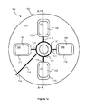
- Figure 1a shows an electrical module 100 according to an embodiment of the invention.
- Figure 1b shows a section view A - A of the electrical module in an exemplifying situation in which the electrical module is between electrical conductor elements 127 and 128.
- the electrical conductor elements 127 and 128 are arranged to press the electrical module in a direction perpendicular to surfaces 125 and 126 of the electrical conductor elements.
- the electrical module comp rises electrical components 102-105.
- Each of the electrical components has a first contact surface 106-109 that is capable of forming a galvanic contact with the electrical conductor element 127.
- the electrical module comprises a holder element 101 including flexible material that is arranged to support the electrical components with respect to each other in such a way that the first contact surfaces of the electrical components are capable of aligning with the surface 125 independently of each other.
- the fact that the electrical components 102-105 are supported in a flexible manner with respect to each other allows a greater tolerance between the shape of the surface 125 and an ideal plane.
- the electrical components have second contact surfaces, e.g. 122 and 123 in figure 1b , on opposite sides of the electrical components with respect to the first contact surfaces.
- the second contact surfaces are capable of forming galvanic contacts with the electrical conductor element 128.
- the electrical module 100 contains four electrical components 102-105. It should be noted that in a general case, the number of electrical components of an electrical module according to this embodiment of the invention can be any number greater than one.
- An electrical component 102, 103, 104, and/or 105 of the electrical module can be, for example, a diode, a thyristor, a gate turn-off thyristor (GTO), a field effect transistor (FET), a bipolar transistor, or an insulated gate bipolar transistor (IGBT).
- the electrical components of the electrical module can be mutually similar or some electrical components can be different from some other electrical components.
- An electrical component 102, 103, 104, and/or 105 of the electrical module can be as well a combination of two or more different sub-components.
- an electrical component of the electrical module can be an antiparallel pair of a diode and a thyristor, an antiparallel pair of a diode and a gate turn-off thyristor (GTO), an antiparallel pair of a diode and a field effect transistor (FET), an antiparallel pair of a diode and a bipolar transistor, or an antiparallel pair of a diode and an insulated gate bipolar transistor (IGBT).
- GTO gate turn-off thyristor
- FET field effect transistor
- IGBT antiparallel pair of a diode and a bipolar transistor
- IGBT insulated gate bipolar transistor
- An electrical component 102, 103, 104, and/or 105 of the electrical module can be as well a monolithic component that is arranged to realize functionality of two or more different electrical components, e.g. functionalities of a diode and an IGBT.
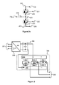
- Figure 1c shows a circuit diagram that corresponds to figure 1b .
- the electrical components 102-105 are depicted with ovals in figure 1c .
- the reference numbers in figure 1c correspond to same entities as in figures 1a and 1b .
- the circuit diagram illustrates how the electrical components 102-105 are parallel connected between the electrical conductor elements 127 and 128. Due to the fact that the holder element 101 is capable of supporting the electrical components 102-105 in a flexible manner, the electrical components 102-105 are pressed against the surfaces 127 and 128 in a sufficiently uniform manner. This fact is important from the viewpoint of balanced division of electrical current i between the electrical components 102-105 and from the viewpoint of thermal conductivity between the electrical components and the electrical conductor elements 127 and 128.
- the holder element 101 is made of flexible material.
- the holder element can be made of, for example, silicone, epoxy, plastic or a suitable composition of two or more of the said materials.
- suitable silicone materials are SE2003, QSil573 and AS1420 by ACC Silicones, and SOLARITE SI221FR and SOLARITE SI222HTC by Solar compounds.
- suitable epoxy materials are 20-3006 and 20-3001 by Epoxies etc, Circalok 6031 A/B by Lord, and Scotchcast 280 by 3M.
- the holder element can also be made of suitable hot melt adhesive.
- the holder element should maintain its flexibility at least till the time the electrical module has been installed into a product, e.g. into a frequency converter.
- the material of the holder element 101 is preferably able to withstand temperatures up to about 175°C.
- Figures 1d and 1e show an illustration of installing an electrical module whose holder element 101 is made of flexible material.
- Figure 1d shows an exemplifying situation in which the contact surfaces of the electrical components 102 and 103 are not aligned according to a same plane.
- the misalignment of the electrical components may be e.g. a consequence of limited manufacturing accuracy.
- Figure 1e shows a situation that takes place after the electrical module is pressed between the surfaces 125 and 126 of the electrical conductor elements 127 and 128.
- the flexible material of the holder element 101 is elastic in such a way that each electrical component is able to align with the surfaces 125 and 126 independently of the other electrical components of the electrical module.
- misalignment of the electrical components is exaggerated for illustrative purposes.
- the holder element comprises both rigid material and flexible material.
- the flexible material is located between the electrical components 102-105 and a part of the holder element that is made of the rigid material.
- the flexible material provides the flexible support for the electrical components.
- the flexible material can be e.g. silicone, epoxy, plastic, or a suitable composition of two or more of the said materials.
- the flexible material can also contain e.g. suitable hot melt adhesive.
- the flexible material should maintain its flexibility at least till the time the electrical module has been installed into a product, e.g. into a frequency converter.
- the flexible material is preferably able to withstand temperatures up to about 175°C.
- the holder element 101 is made of electrically insulating material. In this case it can be allowed that the holder element is in touch with the first and/or second contact surfaces of the electrical components 102-105.
- the holder element 101 comprises electrically insulating material 117-120 between a body 144 of the holder element and the first and second contact surfaces of the electrical components 102-105.
- the body of the holder element is made of electrically insulating material.
- the body 144 of the holder element can be made of rigid material if the electrically insulating material 117-120 is suff i-ciently flexible material.
- An electrical module comprises a control terminal 116 that is common to the electrical components 102-105.
- Electrical conductors 110-115 from the control terminal to the electrical components can be, for example, inside the holder element or the electrical conductors can be on a surface of the holder element.
- the holder element 101 comprises a hole 121.
- the hole can be utilized e.g. when installing the electrical module between the electrical conductor elements 127 and 128.
- the electrical conductor element 127 comprises an overhang 129 that fits into the hole.
- Figure 2a shows an electrical module 200 according to an embodiment of the invention.
- Figure 2b shows a section view A - A of the electrical module in an exemplifying situation in which the electrical module is between a support element 228 and a connection element 227 that comprises electrical conductor plates 234, 235, and 236.
- the support element 228 and the connection element 227 are arranged to press the electrical module in a direction perpendicular to a surface 225.
- the electrical module comprises electrical components 202 and 203.
- the electrical component 202 has a contact surface 206 that is capable of forming a galvanic contact with the electrical conductor plate 234.
- the electrical component 203 has a contact surface 207 that is capable of forming a galvanic contact with the electrical conductor plate 235.
- the electrical module comprises an electrical conductor plate 240 that has a contact surface 230 capable of forming a galvanic contact with the electrical conductor plate 236.
- the electrical module comprises an electrical conductor 233 that is arranged to connect one terminal of the electrical component 202 to the contact surface 230 and one terminal of the electrical component 203 to the contact surface 230.
- the electrical components 202 and 203 are antiparallel pairs of a diode and an insulated gate bipolar transistor (IGBT).
- Figure 2c shows a circuit diagram that corresponds to figures 2a and 2b .
- the reference numbers in figure 2c correspond to same entities as in figures 2a and 2b .
- the electrical module comprises control terminals 231 and 232 that are connected to the gates of the electrical components 202 and 203, respectively.
- the electrical module can constitute, for example, an output phase of an inverter bridge.
- the electrical module 200 comprises a holder element 201 that includes flexible material arranged to flexibly support the electrical components 202 and 203 and the electrical conductor plate 240 with respect to each other in such a way that the contact surfaces 206 and 207 of the electrical components and the contact surface 230 of the electrical conductor plate 240 are capable of aligning with surfaces of the electrical conductor plates 234, 235, 236 independently of each others.
- Figure 2b illustrates a situation in which the surfaces of the electrical conductor plates 234, 235, 236 are not in a same plane and, as a consequence, the electrical components 202 and 203 and the electrical conductor plate 240 are individually aligned with the surfaces of the electrical conductor plates 234, 235, 236.
- the deviation of the surfaces of the electrical conductor plates 234, 235, 236 from the same plane is exaggerated for illustrative purposes.
- the holder element 201 is provided with grooves 260 or fins that are arranged to increase creeping distances between the electrical components 202 and 203 and/or between the electrical components and the electrical conductor plate 240. It is also possible that physical dimensions of the holder element 201 are selected in such a way that sufficient creeping distances are obtained.
- An electrical converter device comprises at least one an electrical module according to an embodiment of the invention.
- Figure 3 shows an electrical converter device according to an embodiment of the invention.
- the electrical converter device comprises an electrical terminal 351 for connecting the electrical converter device to an alternating voltage network (not shown) and an electrical terminal 352 for connecting the electrical converter device to a load (not shown).
- the electrical converter device comprises a converter unit 353 that can be e.g. a rectifier that is arranged to transfer energy from an alternating voltage network to an intermediate circuit 366 of the electrical converter device.
- the converter unit 353 can be as well a device that is capable of transferring energy, not only from the alternating voltage network to the intermediate circuit 366, but also from the intermediate circuit back to the alternating voltage network.
- the electrical converter device comprises an inverter bridge 354 that is able to transfer energy from the intermediate circuit 366 to the load and also to transfer energy from the load to the intermediate circuit.
- the main circuit of the inverter bridge comprises electrical conductor elements 355 and 356 that are connected to the intermediate circuit, and electrical conductor elements 357, 358, and 359 that are connected to different phases of the electrical terminal 352.
- the main circuit of the inverter bridge comprises electrical modules 360-365 that are located between the electrical conductor elements as shown in figure 10. Each of the electrical modules 360-365 comprises:
- the electrical modules 360-365 can be, for example, according to what is described in figures 1 a and 1 b and in the text passages related to figures 1 a and 1 b.
- the electrical module 360 may correspond to the electrical module depicted in figures 1 a and 1b
- the electrical conductor elements 355 and 357 may correspond to the electrical conductor elements 127 and 128 depicted in figure 1b .
- the electrical converter device shown in figure 3 is a frequency converter.
- An electrical converter device according to an embodiment of the invention can be as well, for example, a mere inverter or a mere rectifier.
- Figure 4 is a flow chart of a method according to an embodiment of the invention for assembling an electrical converter device.
- One of the method phases for assembling the electrical converter device comprises installing 401, as an element of the electrical converter device, at least one electrical module (e.g. 100 in figure 1 a) that comprises:
- each of the electrical components of the electrical module has a second contact surface (e.g. 122 and 123 in figure 1a ) on an opposite side of that electrical component with respect to the first contact surface of that electrical component, the second contact surface being capable of forming a galvanic contact with another external electrical conductor.
- a second contact surface e.g. 122 and 123 in figure 1a
- each of the electrical components of the electrical module is one of the following: a diode, a thyristor, a gate turn-off thyristor (GTO), a field effect transistor (FET), a bipolar transistor, and an insulated gate bipolar transistor (IGBT).
- GTO gate turn-off thyristor
- FET field effect transistor
- IGBT insulated gate bipolar transistor
- each of the electrical components of the electrical module is one of the following: an antiparallel pair of a diode and a thyristor, an antiparallel pair of a diode and a gate turn-off thyristor (GTO), an antiparallel pair of a diode and a field effect transistor (FET), an antiparallel pair of a diode and a bipolar transistor, and an antiparallel pair of a diode and an insulated gate bipolar transistor (IGBT).
- GTO gate turn-off thyristor
- FET field effect transistor
- IGBT antiparallel pair of a diode and a bipolar transistor
- IGBT insulated gate bipolar transistor
- one of the following is used as the flexible material of the holder element: silicone, epoxy, and plastic.
- hot melt adhesive is used as the flexible material of the holder element.
- the holder element is made of electrically insulating material.
- the holder element comprises electrically insulating material (e.g. 117-120 in figure 1a ) between a body (e.g. 144 in figure 1a ) of the holder element and the first and second contact surfaces of the electrical components.
- the electrical module comprises a control terminal (e.g. 116 in figure 1a ) that is common to the electrical components of the electrical module.
- Electrical conductors e.g. 110-115 in figure 1a
- the control terminal can be, for example, inside or on a surface of the holder element.
- the holder element comprises a hole (e.g. 121 in figure 1a ) that makes the installation of the electrical module easier.
Landscapes
- Inverter Devices (AREA)
Abstract
Description
- The invention relates to a mechanical construction of an electrical module that comprises two or more electrical components. Furthermore, the invention relates to an electrical converter device comprising one or more electrical modules and to a method for assembling an electrical converter device.
- An assembly process of an electrical converter device, e.g. a frequency converter, can be made simpler, faster, and more cost effective by using electrical modules that contain two or more electrical components such as, for example, diodes and/or insulated gate bipolar transistors (IGBT). In an assembly process of an electrical converter device it is significantly faster, simpler, and more cost effective to install a single electrical module than to install a corresponding amount of separate electrical components such as e.g. diodes and IGBTs.
- Certain electrical components, especially high power electrical components, are installed in such a way that an electrical component is pressed against a surface of an electrical conductor element that forms a galvanic contact with a contact surface of the electrical component. The said contact surface represents an electrical terminal of the electrical component, e.g. a cathode or an anode of a diode, an emitter or a collector of a bipolar transistor, or a drain or a source of a field effect transistor. As the output power and thus the current rating of an electrical converter device increases, parallel connection of the electrical components becomes usually inevitable. In the situation in which there are parallel connected electrical components, it is important that all the electrical components are pressed against an electrical conductor element in a sufficiently uniform manner with regard to pressing forces and mutual alignments between contact surfaces of the electrical components and the surface of the electrical conductor el ement. The above-mentioned facts are important from the viewpoint of balance of electrical current division between the parallel connected electrical components and from the viewpoint of thermal conductivity between the electrical components and the electrical conductor element. The requirements related to pressing forces and to mutual alignments between contact surfaces of electrical components and a surface of an electrical conductor element complicate the applicability of multi-component electrical modules and limit the amount of electrical components that can be integrated into a single electrical module. When using a multi-component electrical module it is more challenging to guarantee that all electrical components of the multi-component electrical module are pressed against an electrical conductor element in a sufficiently uniform manner than when using separate electrical components.
- In accordance with a first aspect of the invention, there is provided a new electrical module. The electrical module comprises:
- two or more electrical components, each of the electrical components having a contact surface that is capable of forming a galvanic contact with an external electrical conductor, and
- a holder element including flexible material arranged to support the electrical components with respect to each other in such a way that the contact surfaces of the electrical components are capable of aligning with external surfaces independently of each other.
- Each electrical component of the electrical module is able to align with e.g. a surface of an electrical conductor element independently of other electrical components. Therefore, it is easier to guarantee that all the electrical components of the electrical module are pressed against e.g. the surface of the electrical conductor element in a sufficiently uniform manner and, as a consequence, a need for derating the electrical components of the electrical module with respect to rating of corresponding separate electrical components is usually mitigated.
- In accordance with a second aspect of the invention, there is provided a new electrical converter device. The electrical converter device comprises at least one an electrical module according to the invention. The electrical converter device can be, e.g. an inverter, a rectifier, and/or a frequency converter.
- In accordance with a third aspect of the invention, there is provided a new method for assembling an electrical converter device. The method comprises installing, as an element of the electrical converter device, at least one electrical module that comprises:
- two or more electrical components, each of the electrical components having a contact surface that is capable of forming a galvanic contact with an external electrical conductor, and
- a holder element,
- A number of exemplifying embodiments of the invention are described in accompanied dependent claims.
- Various embodiments of the invention both as to constructions and to methods of operation, together with additional objects and advantages thereof, will be best understood from the following description of specific exemplifying embodiments when read in connection with the accompanying drawings.
- The exemplifying embodiments of the invention presented in this document are not to be interpreted to pose limitations to the applicability of the appended claims. The verb "to comprise" is used in this document as an open limitation that does not exclude the existence of also unrecited features. The features recited in depending claims are mutually freely combinable unless otherwise explicitly stated.
- The exemplifying embodiments of the invention and their advantages are explained in greater detail below in the sense of examples and with reference to the accompanying drawings, in which:
-
figures 1a ,1b ,1c ,1d, and 1e show an electrical module according to an embodiment of the invention, a section view of the electrical module in an exemplifying operating environment, a circuit diagram that corresponds tofigure 1b , and an illustration of installing the electrical module, -
figures 2a ,2b , and2c show an electrical module according to an embodiment of the invention, a section view of the electrical module in an exemplifying operating environment, and an exemplifying circuit diagram that corresponds tofigure 2b , -
figure 3 shows an electrical converter device according to an embodiment of the invention, and -
figure 4 is a flow chart of a method according to an embodiment of the invention for assembling an electrical converter device. -
Figure 1a shows anelectrical module 100 according to an embodiment of the invention.Figure 1b shows a section view A - A of the electrical module in an exemplifying situation in which the electrical module is betweenelectrical conductor elements electrical conductor elements surfaces electrical conductor element 127. The electrical module comprises aholder element 101 including flexible material that is arranged to support the electrical components with respect to each other in such a way that the first contact surfaces of the electrical components are capable of aligning with thesurface 125 independently of each other. The fact that the electrical components 102-105 are supported in a flexible manner with respect to each other allows a greater tolerance between the shape of thesurface 125 and an ideal plane. The electrical components have second contact surfaces, e.g. 122 and 123 infigure 1b , on opposite sides of the electrical components with respect to the first contact surfaces. The second contact surfaces are capable of forming galvanic contacts with theelectrical conductor element 128. Theelectrical module 100 contains four electrical components 102-105. It should be noted that in a general case, the number of electrical components of an electrical module according to this embodiment of the invention can be any number greater than one. - An
electrical component - An
electrical component electrical component -
Figure 1c shows a circuit diagram that corresponds tofigure 1b . The electrical components 102-105 are depicted with ovals infigure 1c . The reference numbers infigure 1c correspond to same entities as infigures 1a and1b . The circuit diagram illustrates how the electrical components 102-105 are parallel connected between theelectrical conductor elements holder element 101 is capable of supporting the electrical components 102-105 in a flexible manner, the electrical components 102-105 are pressed against thesurfaces electrical conductor elements - In an electrical module according to an embodiment of the invention, the
holder element 101 is made of flexible material. The holder element can be made of, for example, silicone, epoxy, plastic or a suitable composition of two or more of the said materials. Some examples of suitable silicone materials are SE2003, QSil573 and AS1420 by ACC Silicones, and SOLARITE SI221FR and SOLARITE SI222HTC by Solar compounds. Examples of suitable epoxy materials are 20-3006 and 20-3001 by Epoxies etc, Circalok 6031 A/B by Lord, and Scotchcast 280 by 3M. The holder element can also be made of suitable hot melt adhesive. The holder element should maintain its flexibility at least till the time the electrical module has been installed into a product, e.g. into a frequency converter. The material of theholder element 101 is preferably able to withstand temperatures up to about 175°C. -
Figures 1d and 1e show an illustration of installing an electrical module whoseholder element 101 is made of flexible material.Figure 1d shows an exemplifying situation in which the contact surfaces of theelectrical components Figure 1e shows a situation that takes place after the electrical module is pressed between thesurfaces electrical conductor elements holder element 101 is elastic in such a way that each electrical component is able to align with thesurfaces figure 1d th e misalignment of the electrical components is exaggerated for illustrative purposes. - In an electrical module according to an embodiment of the invention, the holder element comprises both rigid material and flexible material. The flexible material is located between the electrical components 102-105 and a part of the holder element that is made of the rigid material. The flexible material provides the flexible support for the electrical components. The flexible material can be e.g. silicone, epoxy, plastic, or a suitable composition of two or more of the said materials. The flexible material can also contain e.g. suitable hot melt adhesive. The flexible material should maintain its flexibility at least till the time the electrical module has been installed into a product, e.g. into a frequency converter. The flexible material is preferably able to withstand temperatures up to about 175°C.
- In an electrical module according to an embodiment of the invention, the
holder element 101 is made of electrically insulating material. In this case it can be allowed that the holder element is in touch with the first and/or second contact surfaces of the electrical components 102-105. - In an electrical module according to an embodiment of the invention, the
holder element 101 comprises electrically insulating material 117-120 between abody 144 of the holder element and the first and second contact surfaces of the electrical components 102-105. In this case it is not necessary that the body of the holder element is made of electrically insulating material. Furthermore, in the electrical module shown infigures 1 a and 1 b, thebody 144 of the holder element can be made of rigid material if the electrically insulating material 117-120 is suff i-ciently flexible material. - An electrical module according to an embodiment of the invention comprises a
control terminal 116 that is common to the electrical components 102-105. Electrical conductors 110-115 from the control terminal to the electrical components can be, for example, inside the holder element or the electrical conductors can be on a surface of the holder element. - In an electrical module according to an embodiment of the invention, the
holder element 101 comprises ahole 121. The hole can be utilized e.g. when installing the electrical module between theelectrical conductor elements electrical conductor element 127 comprises anoverhang 129 that fits into the hole. -
Figure 2a shows anelectrical module 200 according to an embodiment of the invention.Figure 2b shows a section view A - A of the electrical module in an exemplifying situation in which the electrical module is between asupport element 228 and aconnection element 227 that compriseselectrical conductor plates support element 228 and theconnection element 227 are arranged to press the electrical module in a direction perpendicular to asurface 225. The electrical module compriseselectrical components electrical component 202 has acontact surface 206 that is capable of forming a galvanic contact with theelectrical conductor plate 234. Theelectrical component 203 has acontact surface 207 that is capable of forming a galvanic contact with theelectrical conductor plate 235. The electrical module comprises anelectrical conductor plate 240 that has acontact surface 230 capable of forming a galvanic contact with theelectrical conductor plate 236. The electrical module comprises anelectrical conductor 233 that is arranged to connect one terminal of theelectrical component 202 to thecontact surface 230 and one terminal of theelectrical component 203 to thecontact surface 230. In this exemplifying embodiment of the invention theelectrical components Figure 2c shows a circuit diagram that corresponds tofigures 2a and2b . The reference numbers infigure 2c correspond to same entities as infigures 2a and2b . The electrical module comprisescontrol terminals electrical components - The
electrical module 200 comprises aholder element 201 that includes flexible material arranged to flexibly support theelectrical components electrical conductor plate 240 with respect to each other in such a way that the contact surfaces 206 and 207 of the electrical components and thecontact surface 230 of theelectrical conductor plate 240 are capable of aligning with surfaces of theelectrical conductor plates Figure 2b illustrates a situation in which the surfaces of theelectrical conductor plates electrical components electrical conductor plate 240 are individually aligned with the surfaces of theelectrical conductor plates figure 2b , the deviation of the surfaces of theelectrical conductor plates - In an electrical module according to an embodiment of the invention the
holder element 201 is provided withgrooves 260 or fins that are arranged to increase creeping distances between theelectrical components electrical conductor plate 240. It is also possible that physical dimensions of theholder element 201 are selected in such a way that sufficient creeping distances are obtained. - An electrical converter device according to an embodiment of the invention comprises at least one an electrical module according to an embodiment of the invention.
Figure 3 shows an electrical converter device according to an embodiment of the invention. The electrical converter device comprises anelectrical terminal 351 for connecting the electrical converter device to an alternating voltage network (not shown) and anelectrical terminal 352 for connecting the electrical converter device to a load (not shown). The electrical converter device comprises aconverter unit 353 that can be e.g. a rectifier that is arranged to transfer energy from an alternating voltage network to anintermediate circuit 366 of the electrical converter device. Theconverter unit 353 can be as well a device that is capable of transferring energy, not only from the alternating voltage network to theintermediate circuit 366, but also from the intermediate circuit back to the alternating voltage network. - The electrical converter device comprises an
inverter bridge 354 that is able to transfer energy from theintermediate circuit 366 to the load and also to transfer energy from the load to the intermediate circuit. The main circuit of the inverter bridge compriseselectrical conductor elements electrical conductor elements electrical terminal 352. The main circuit of the inverter bridge comprises electrical modules 360-365 that are located between the electrical conductor elements as shown in figure 10. Each of the electrical modules 360-365 comprises: - two or more electrical components, each of the electrical components having contact surfaces that are capable of forming galvanic contacts with electrical conductor elements between which the electrical module in question is located, and
- a holder element including flexible material arranged to support the electrical components with respect to each other in such a way that the electrical components are capable of aligning, independently of each other, with the electrical conductor elements between which the electrical module in question is located.
- The electrical modules 360-365 can be, for example, according to what is described in
figures 1 a and 1 b and in the text passages related tofigures 1 a and 1 b. For example, theelectrical module 360 may correspond to the electrical module depicted infigures 1 a and 1b, and theelectrical conductor elements electrical conductor elements figure 1b . - The electrical converter device shown in
figure 3 is a frequency converter. An electrical converter device according to an embodiment of the invention can be as well, for example, a mere inverter or a mere rectifier. -
Figure 4 is a flow chart of a method according to an embodiment of the invention for assembling an electrical converter device. One of the method phases for assembling the electrical converter device comprises installing 401, as an element of the electrical converter device, at least one electrical module (e.g. 100 infigure 1 a) that comprises: - two or more electrical components (e.g. 102-105 in
figures 1 a and 1 b), each of the electrical components having a first contact surface (e.g. 106-109 infigure 1a ) that is capable of forming a galvanic contact with an external electrical conductor (e.g. 127 infigure 1 b) , and - a holder element (e.g. 101 in
figures 1 a and 1 b), - In a method according to an embodiment of the invention, each of the electrical components of the electrical module has a second contact surface (e.g. 122 and 123 in
figure 1a ) on an opposite side of that electrical component with respect to the first contact surface of that electrical component, the second contact surface being capable of forming a galvanic contact with another external electrical conductor. - In a method according to an embodiment of the invention, each of the electrical components of the electrical module is one of the following: a diode, a thyristor, a gate turn-off thyristor (GTO), a field effect transistor (FET), a bipolar transistor, and an insulated gate bipolar transistor (IGBT).
- In a method according to an embodiment of the invention, each of the electrical components of the electrical module is one of the following: an antiparallel pair of a diode and a thyristor, an antiparallel pair of a diode and a gate turn-off thyristor (GTO), an antiparallel pair of a diode and a field effect transistor (FET), an antiparallel pair of a diode and a bipolar transistor, and an antiparallel pair of a diode and an insulated gate bipolar transistor (IGBT).
- In a method according to an embodiment of the invention, one of the following is used as the flexible material of the holder element: silicone, epoxy, and plastic.
- In a method according to an embodiment of the invention, hot melt adhesive is used as the flexible material of the holder element.
- In a method according to an embodiment of the invention, the holder element is made of electrically insulating material.
- In a method according to an embodiment of the invention, the holder element comprises electrically insulating material (e.g. 117-120 in
figure 1a ) between a body (e.g. 144 infigure 1a ) of the holder element and the first and second contact surfaces of the electrical components. - In a method according to an embodiment of the invention, the electrical module comprises a control terminal (e.g. 116 in
figure 1a ) that is common to the electrical components of the electrical module. Electrical conductors (e.g. 110-115 infigure 1a ) from the control terminal to the electrical components can be, for example, inside or on a surface of the holder element. - In a method according to an embodiment of the invention the holder element comprises a hole (e.g. 121 in
figure 1a ) that makes the installation of the electrical module easier. - While there have been shown and described and pointed out fundamental novel features of the invention as applied to embodiments thereof, it will be understood that various omissions and substitutions and changes in the form and details of the devices and methods described may be made by those skilled in the art without departing from the spirit of the invention. For example, it is expressly intended that all combinations of those elements and/or method steps which perform substantially the same function in substantially the same way to achieve the same results are within the scope of the invention. Moreover, it should be recognized that structures and/or elements and/or method steps shown and/or described in connection with any disclosed form or embodiment of the invention may be incorporated in any other disclosed or described or suggested form or embodiment as a general matter of design choice. The specific examples provided in the description given above should not be construed as limiting. Therefore, the invention is not limited merely to the embodiments described above, many variants being possible without departing from the scope of the inventive idea defined in the independent claims.
Claims (15)
- An electrical module comprising two or more electrical components (102-105, 202, 203), each of the electrical components having a first contact surface (106-109, 206, 207) capable of forming a galvanic contact with an external electrical conductor, characterized in that the electrical module comprises a holder element (101, 201) including flexible material arranged to support the electrical components with respect to each other in such a way that the first contact surfaces of the electrical components are capable of aligning with external surfaces independently of each other.
- An electrical module according to claim 1, wherein each of the electrical components has a second contact surface (122, 123) on an opposite side of that electrical component with respect to the first contact surface of that electrical component, the second contact surface being capable of forming a galvanic contact with another external electrical conductor.
- An electrical module according to claim 1, wherein each of the electrical components is one of the following: a diode, a thyristor, a gate turn-off thyristor (GTO), a field effect transistor (FET), a bipolar transistor, and an insulated gate bipolar transistor (IGBT).
- An electrical module according to claim 1, wherein each of the electrical components is one of the following: an antiparallel pair of a diode and a thyristor, an antiparallel pair of a diode and a gate turn-off thyristor (GTO), an antiparallel pair of a diode and a field effect transistor (FET), an antiparallel pair of a diode and a bipolar transistor, and an antiparallel pair of a diode and an insulated gate bipolar transistor (IGBT).
- An electrical module according to claim 1, wherein the flexible material of the holder element contains at least one of the following: silicone, epoxy, and plastic.
- An electrical module according to claim 1, wherein the flexible material of the holder element contains hot melt adhesive.
- An electrical module according to claim 1, wherein the holder element is made of electrically insulating material.
- An electrical module according to claim 1, wherein the holder element comprises electrically insulating material (117-120) between a body (144) of the holder element and the first contact surfaces of the electrical components.
- An electrical module according to claim 1, wherein the electrical module comprises a control terminal (116) common to the electrical components, and electrical conductors (110-115) from the control terminal to the electrical components are inside the holder element.
- An electrical module according to claim 1, wherein the electrical module comprises a control terminal (116) common to the electrical components, and electrical conductors (110-115) from the control terminal to the electrical components are on a surface of the holder element.
- An electrical module according to claim 1, wherein the electrical module comprises a separate control terminal (231, 232) for at least one of the electrical components ( 202, 203), each separate control terminal being electrically connected to at least one of the electrical components.
- An electrical module according to claim 1, wherein the holder element comprises a hole (121).
- An electrical module according to claim 1, wherein the electrical module comprises an electrical conductor (233) arranged to electrically connect an electrical terminal of one electrical component (202) of the electrical module to an electrical terminal of another electrical component (203) of the electrical module.
- An electrical converter device, characterized in that the electrical converter device comprises at least one an electrical module (360-365) according to claim 1.
- A method for assembling an electrical converter device, characterized in that the method comprises installing (401), as an element of the electrical converter device, at least one electrical module (100) that comprises:- two or more electrical components (102-105), each of the electrical components having a contact surface (106-109) that is capable of forming a galvanic contact with an external electrical conductor, and- a holder element (101),wherein the holder element includes material that is, at least during the installation of the electrical module, flexible and arranged to support the electrical components of the electrical module with respect to each other in such a way that the contact surfaces of the electrical components are capable of aligning with external surfaces independently of each other.
Priority Applications (2)
| Application Number | Priority Date | Filing Date | Title |
|---|---|---|---|
| EP08151151A EP2088623A1 (en) | 2008-02-07 | 2008-02-07 | A multi-component electrical module |
| US12/366,182 US7968914B2 (en) | 2008-02-07 | 2009-02-05 | Multi-component electrical module |
Applications Claiming Priority (1)
| Application Number | Priority Date | Filing Date | Title |
|---|---|---|---|
| EP08151151A EP2088623A1 (en) | 2008-02-07 | 2008-02-07 | A multi-component electrical module |
Publications (1)
| Publication Number | Publication Date |
|---|---|
| EP2088623A1 true EP2088623A1 (en) | 2009-08-12 |
Family
ID=39564247
Family Applications (1)
| Application Number | Title | Priority Date | Filing Date |
|---|---|---|---|
| EP08151151A Withdrawn EP2088623A1 (en) | 2008-02-07 | 2008-02-07 | A multi-component electrical module |
Country Status (2)
| Country | Link |
|---|---|
| US (1) | US7968914B2 (en) |
| EP (1) | EP2088623A1 (en) |
Citations (4)
| Publication number | Priority date | Publication date | Assignee | Title |
|---|---|---|---|---|
| EP0637080A1 (en) * | 1993-07-27 | 1995-02-01 | Fuji Electric Co. Ltd. | Pressure contact type semiconductor device and assembly method therefor |
| US5926372A (en) * | 1997-12-23 | 1999-07-20 | Ford Global Technologies, Inc. | Power block assembly and method of making same |
| EP0962973A1 (en) * | 1998-06-02 | 1999-12-08 | Fuji Electric Co., Ltd. | Multichip press-contact power semiconductor device |
| US20030001258A1 (en) * | 1998-01-22 | 2003-01-02 | Hironori Kodama | Semiconductor device, including an arrangementto provide a uniform press contact and converter using same |
-
2008
- 2008-02-07 EP EP08151151A patent/EP2088623A1/en not_active Withdrawn
-
2009
- 2009-02-05 US US12/366,182 patent/US7968914B2/en not_active Expired - Fee Related
Patent Citations (4)
| Publication number | Priority date | Publication date | Assignee | Title |
|---|---|---|---|---|
| EP0637080A1 (en) * | 1993-07-27 | 1995-02-01 | Fuji Electric Co. Ltd. | Pressure contact type semiconductor device and assembly method therefor |
| US5926372A (en) * | 1997-12-23 | 1999-07-20 | Ford Global Technologies, Inc. | Power block assembly and method of making same |
| US20030001258A1 (en) * | 1998-01-22 | 2003-01-02 | Hironori Kodama | Semiconductor device, including an arrangementto provide a uniform press contact and converter using same |
| EP0962973A1 (en) * | 1998-06-02 | 1999-12-08 | Fuji Electric Co., Ltd. | Multichip press-contact power semiconductor device |
Also Published As
| Publication number | Publication date |
|---|---|
| US20090201659A1 (en) | 2009-08-13 |
| US7968914B2 (en) | 2011-06-28 |
Similar Documents
| Publication | Publication Date | Title |
|---|---|---|
| KR101755769B1 (en) | Dual side cooling power module and Method for manufacturing the same | |
| EP2725609B1 (en) | Semiconductor module | |
| CN105097716A (en) | Power semiconductor module with switching device and assembly | |
| US9001518B2 (en) | Power module with press-fit clamps | |
| JP2003197864A (en) | Power semiconductor module | |
| JP6474790B2 (en) | Spacer system for semiconductor switching devices | |
| WO2011016360A1 (en) | Power converter | |
| EP3370255A1 (en) | Power conversion device | |
| US9437508B2 (en) | Method for manufacturing semiconductor device and semiconductor device | |
| CN101438403A (en) | Semiconductor device and method for manufacturing same | |
| US20210367526A1 (en) | Packaged power module | |
| US10811337B2 (en) | Semiconductor device and power convertor | |
| KR20150036347A (en) | Semiconductor device | |
| JP2017531924A (en) | Semiconductor module and stack arrangement of semiconductor modules | |
| US7968914B2 (en) | Multi-component electrical module | |
| WO2018050713A1 (en) | Press-pack power module | |
| KR20220113415A (en) | Electrical Assemblies and Voltage Converters | |
| JP2013128065A (en) | Wiring body with wiring sheet, semiconductor device, and method for manufacturing the semiconductor device | |
| US12446197B2 (en) | Voltage converter and method for manufacturing a voltage converter | |
| CN113328605B (en) | Power conversion device | |
| EP2017887A1 (en) | Package for electronic components and method for packaging semiconductor devices | |
| JP2001230373A (en) | Flat semiconductor device and power converter using the same | |
| CN118589881A (en) | Half-bridge switch components | |
| WO2025079490A1 (en) | Power conversion device | |
| WO2025079556A1 (en) | Electric power converter |
Legal Events
| Date | Code | Title | Description |
|---|---|---|---|
| PUAI | Public reference made under article 153(3) epc to a published international application that has entered the european phase |
Free format text: ORIGINAL CODE: 0009012 |
|
| AK | Designated contracting states |
Kind code of ref document: A1 Designated state(s): AT BE BG CH CY CZ DE DK EE ES FI FR GB GR HR HU IE IS IT LI LT LU LV MC MT NL NO PL PT RO SE SI SK TR |
|
| AX | Request for extension of the european patent |
Extension state: AL BA MK RS |
|
| 17P | Request for examination filed |
Effective date: 20090901 |
|
| AKX | Designation fees paid |
Designated state(s): AT BE BG CH CY CZ DE DK EE ES FI FR GB GR HR HU IE IS IT LI LT LU LV MC MT NL NO PL PT RO SE SI SK TR |
|
| 17Q | First examination report despatched |
Effective date: 20160121 |
|
| STAA | Information on the status of an ep patent application or granted ep patent |
Free format text: STATUS: THE APPLICATION IS DEEMED TO BE WITHDRAWN |
|
| 18D | Application deemed to be withdrawn |
Effective date: 20180901 |