EP2088617A1 - Methods and apparatus for manufacturing semiconductor wafers - Google Patents
Methods and apparatus for manufacturing semiconductor wafers Download PDFInfo
- Publication number
- EP2088617A1 EP2088617A1 EP09151743A EP09151743A EP2088617A1 EP 2088617 A1 EP2088617 A1 EP 2088617A1 EP 09151743 A EP09151743 A EP 09151743A EP 09151743 A EP09151743 A EP 09151743A EP 2088617 A1 EP2088617 A1 EP 2088617A1
- Authority
- EP
- European Patent Office
- Prior art keywords
- melt
- release coating
- setter
- semiconductor
- predetermined
- Prior art date
- Legal status (The legal status is an assumption and is not a legal conclusion. Google has not performed a legal analysis and makes no representation as to the accuracy of the status listed.)
- Withdrawn
Links
Images



Classifications
-
- H—ELECTRICITY
- H10—SEMICONDUCTOR DEVICES; ELECTRIC SOLID-STATE DEVICES NOT OTHERWISE PROVIDED FOR
- H10F—INORGANIC SEMICONDUCTOR DEVICES SENSITIVE TO INFRARED RADIATION, LIGHT, ELECTROMAGNETIC RADIATION OF SHORTER WAVELENGTH OR CORPUSCULAR RADIATION
- H10F71/00—Manufacture or treatment of devices covered by this subclass
-
- C—CHEMISTRY; METALLURGY
- C30—CRYSTAL GROWTH
- C30B—SINGLE-CRYSTAL GROWTH; UNIDIRECTIONAL SOLIDIFICATION OF EUTECTIC MATERIAL OR UNIDIRECTIONAL DEMIXING OF EUTECTOID MATERIAL; REFINING BY ZONE-MELTING OF MATERIAL; PRODUCTION OF A HOMOGENEOUS POLYCRYSTALLINE MATERIAL WITH DEFINED STRUCTURE; SINGLE CRYSTALS OR HOMOGENEOUS POLYCRYSTALLINE MATERIAL WITH DEFINED STRUCTURE; AFTER-TREATMENT OF SINGLE CRYSTALS OR A HOMOGENEOUS POLYCRYSTALLINE MATERIAL WITH DEFINED STRUCTURE; APPARATUS THEREFOR
- C30B13/00—Single-crystal growth by zone-melting; Refining by zone-melting
- C30B13/16—Heating of the molten zone
-
- C—CHEMISTRY; METALLURGY
- C30—CRYSTAL GROWTH
- C30B—SINGLE-CRYSTAL GROWTH; UNIDIRECTIONAL SOLIDIFICATION OF EUTECTIC MATERIAL OR UNIDIRECTIONAL DEMIXING OF EUTECTOID MATERIAL; REFINING BY ZONE-MELTING OF MATERIAL; PRODUCTION OF A HOMOGENEOUS POLYCRYSTALLINE MATERIAL WITH DEFINED STRUCTURE; SINGLE CRYSTALS OR HOMOGENEOUS POLYCRYSTALLINE MATERIAL WITH DEFINED STRUCTURE; AFTER-TREATMENT OF SINGLE CRYSTALS OR A HOMOGENEOUS POLYCRYSTALLINE MATERIAL WITH DEFINED STRUCTURE; APPARATUS THEREFOR
- C30B29/00—Single crystals or homogeneous polycrystalline material with defined structure characterised by the material or by their shape
- C30B29/02—Elements
- C30B29/06—Silicon
-
- H—ELECTRICITY
- H10—SEMICONDUCTOR DEVICES; ELECTRIC SOLID-STATE DEVICES NOT OTHERWISE PROVIDED FOR
- H10P—GENERIC PROCESSES OR APPARATUS FOR THE MANUFACTURE OR TREATMENT OF DEVICES COVERED BY CLASS H10
- H10P14/00—Formation of materials, e.g. in the shape of layers or pillars
- H10P14/20—Formation of materials, e.g. in the shape of layers or pillars of semiconductor materials
- H10P14/38—Formation of materials, e.g. in the shape of layers or pillars of semiconductor materials characterised by treatments done after the formation of the materials
- H10P14/3802—Crystallisation or recrystallisation of non-monocrystalline semiconductor materials, e.g. regrowth
Definitions
- This invention relates generally to semiconductor sheets, and more specifically to methods and apparatus for manufacturing semiconductor wafers.
- Wafers formed of semiconductor materials are used in a variety of applications and most, if not all, such applications require an increasing number of such wafers.
- the use of photovoltaic systems has become more common and of greater importance in the production of energy.
- the use of photovoltaic systems is therefore expected to increase dramatically.
- At least some known photovoltaic systems use a semiconductor substrate, such as a substrate consisting of single crystal or poly-crystalline silicon.
- the use of photovoltaic technology may be limited by the cost of semiconductor wafers used in the photovoltaic systems.
- poly-crystalline silicon wafers for use in solar cells are produced by melting a high-purity material in an inert atmosphere.
- the resulting silicon melt is cooled to form a polycrystalline ingot which is then sliced with a wire saw or an inner diameter blade to produce wafers of a desired thickness and size.
- a method for fabricating a semiconductor wafer includes applying a layer of semiconductor material across a portion of a setter material, introducing the setter material and the semiconductor material to a predetermined thermal gradient to form a melt, wherein the thermal gradient includes a predetermined nucleation and growth region, and forming at least one local cold spot in the nucleation and growth region to facilitate inducing crystal nucleation at the at least one desired location.
- a method for fabricating a wafer includes providing a setter, applying a release coating across a top surface of the setter, depositing a semiconductor material across a top surface of the release coating, forming a melt by introducing the release coating and the semiconductor material to a predetermined temperature gradient, and applying a thermal pattern to the melt to induce nucleation in at least one desired location.
- a semiconductor wafer in another aspect, includes a body having a substantially uniform crystallization defined by a predetermined pattern.
- the wafer is fabricated by applying a release coating across a top surface of a setter material, applying at least one layer of at least one semiconductor material across a top surface of the release coating, introducing the setter material, release coating, and the at least one semiconductor material to a predetermined temperature gradient to form a melt across the at least one semiconductor material layer, and forming at least one local cold spot according to the predetermined pattern.
- silicon is one of the most commonly used semiconductor materials, also referred to as feedstock, used in the fabrication of semiconductor wafers. Accordingly, as used herein, the terms “semiconductor” and “semiconductor materials” refer to silicon based components and silicon materials. However, as will be readily appreciated by one of ordinary skill in the art, other semiconductor materials in addition to the silicon materials and/or including non-silicon materials can be fabricated using the apparatus and methods described herein. Although only the use of silicon powder feedstock is described herein for use in fabricating a silicon sheet, liquid silicon feedstock and/or crystallized silicon feedstock may be used without deviating from the present invention.
- FIG. 1 is a schematic diagram of an exemplary fabrication apparatus 100 that may be used to manufacture semiconductor wafers.
- fabrication apparatus 100 is a controlled atmosphere furnace that includes a plurality of zones able to operate with different temperature conditions.
- Fabrication apparatus 100 in the exemplary embodiment, includes a plurality of rollers 104, a hopper 108, a doctor blade 110, and a heating/cooling region 116.
- setter 102 is propelled by rollers 104 to enable setter 102 to be moved under a hopper 108 that deposits a desired quantity of semiconductor material 112, and any desired additives, across a portion of a top surface 118 of setter 102.
- At least one layer of semiconductor material 112 is deposited on top surface 118.
- a second hopper (not shown) may be used to dispense additional semiconductor material 112 across a portion of top surface 118 and/or across a layer of material previously deposited on setter 102. The portion of setter 102 containing semiconductor material 112 is then moved beneath a doctor blade 110 and into heating/cooling region 116.
- heating/cooling region 116 includes at least one thermal treatment device 114.
- Thermal treatment device 114 provides heat energy to heating/cooling region 116 and, thus, induces heat to anything placed within region 116. Any heat source may be used that enables fabrication apparatus 100 to function as described herein.
- heating/cooling region 116 also includes at least one heat extractor 122. Heat extractor 122 removes heat from an object positioned within heating/cooling region 116.
- An inert atmosphere is preferably maintained within an interior of fabrication apparatus 100. More specifically, in the exemplary embodiment, the interior of fabrication apparatus 100 is sealed to facilitate preventing the inert materials from escaping from the fabrication apparatus 100 and/or to prevent the influx of contaminants from external to fabrication apparatus 100.
- Figure 2 is a flow chart illustrating an exemplary method 200 of fabricating a semiconductor wafer 144 using fabrication apparatus 100 (shown in Figure 1 ).
- a setter 102 is initially selected 201. More specifically, the shape of the setter 102 selected determines the shape of the finished semiconductor wafer 144 produced. Accordingly, setter 102 may provide, for example and without limitation, substantially square wafers, substantially circular wafers, and/or substantially rectangular wafers.
- Setter 102 may include one or more recesses (not shown) that have a predetermined shape and/or a predetermined topography that imparts a pattern (not shown in Figures 1 and 2 ) on material layers during the fabrication process.
- setter 102 includes one or more recesses defined on each of a first surface (not shown) and an opposite second surface (not shown). Providing recesses on both the first and second surfaces allows setter 102 to be moved through a furnace, such as apparatus 100, with either side facing upward and with either side against the setter 102.
- a release coating 124 is applied 202 across setter top surface 118 to enable that setter 102 to easily separate from the finished semiconductor wafer 144.
- the release coating 124 is silicon nitride (Si 3 N 4 ).
- Alternative embodiments may use silicon dioxide (SiO 2 ) or silicon carbide (SiC) as a release agent.
- any other ingredient can be used as a release agent that enables wafers 144 to be produced as described herein.
- a liquid slurry containing the release coating 124 is applied to setter 102.
- the release coating 124 may be applied to setter 102 using known application means including, but not limited to, a painting process and/or a spraying process.
- the release coating 124 is applied to setter 102 in a predetermined pattern.
- release coating 124 is applied in a predetermined thickness gradient.
- At least one semiconductor material 112 is then deposited 203 across the release coating 124.
- semiconductor material 112 is deposited 203 after the release coating 124 has dried.
- semiconductor material 112 is deposited in a predetermined amount from a hopper 108, as described above.
- semiconductor material 112 is deposited over release coating 124 with a substantially constant thickness.
- semiconductor material 112 is deposited over release coating 124 in a predetermined pattern and/or with a predetermined thickness gradient.
- thermal profile 140 includes a plurality of regions having varying temperatures and wherein the semiconductor material 112 undergoes physical changes.
- a preheat region 130 occurs after setter 102, including release coating 124 and semiconductor material 112 is passed under doctor blade 110.
- a melt region 132 is then introduced to coating 124 and material 112, such that within melt region 132, the temperature exceeds, by a predetermined amount, the melting temperature of semiconductor material 112.
- melt region 132 At least a top surface 128 of semiconductor material 112 forms a melt 126.
- Setter 102 then enters crystallization region 134, wherein a liquid layer (not shown) and crystallized layer (not shown) coexist.
- the temperature in crystallization region 134 is reduced in a predetermined manner to facilitate crystallization of melt 126.
- the temperature may be modified by positioning and/or repositioning heat sources 114 and/or heat extractor 122.
- Thermal profile 142 also includes a cooling region 136, wherein the crystallized semiconductor material 112 is further cooled.
- the cooled wafers 144 are unloaded from apparatus 100 in a wafer unload region 138.
- a predetermined thermal pattern is applied 205 to melt 126 to induce nucleation of semiconductor material 112 in a predetermined location or locations.
- nucleation is induced by changing the heat transfer properties of melt 126, such that a local cold spot 142 is formed on a surface 128 of melt 126. Inducing nucleation at a local cold spot 142 facilitates an orderly crystal formation within melt 126.
- the heat transfer properties may be changed using a variety of methods.
- release coating 124 may be applied to setter 102 in a predetermined pattern (not shown in Figures 1 and 2 ).
- release coating 124 may be applied to setter 102 in a predetermined thickness gradient.
- the thermal pattern is applied 205 using heat extractor 122, as described below.
- FIG 3 is an illustration of an exemplary heat extractor 122 that may be used with apparatus 100 (shown in Figure 1 ). More specifically, in one embodiment, heat extractor 122 includes a pattern 306, a cooled layer 302, and an insulation layer 304. In an alternative embodiment, cooled layer 302 and insulation layer 304 are composed of substantially different materials and are positioned such that there is no contact between layers 302 and 304. In such an embodiment, insulation layer 304 includes a plurality of holes such that insulation layer 304 acts as a patterned mask between cooled layer 302 and melt 126. Moreover, in one embodiment, cooled layer 302 consists substantially of a metal. In an alternative embodiment, cooled layer 302 consists substantially of graphite.
- heat extractor 122 is positioned within apparatus 100 such that a first surface 308 of heat extractor 122 is closer to melt 126 than an opposite second surface 310 of heat extractor 122. In one embodiment heat extractor 122 is positioned in close proximity to melt 126. In such an embodiment, heat extractor 122 is fabricated substantially from a refractory metal and/or a ceramic material. Alternatively, heat extractor 122 may be fabricated from any material that allows heat extractor 122 to function as described herein. Alternatively, in the embodiment described above, in which heat extractor 122 is positioned in contact with melt 126, heat extractor 122 is fabricated from a material or combination of materials that facilitate preventing melt 126 from adhering to heat extractor 122. Further, heat extractor 122 is fabricated from a material or combination of materials that enables heat extractor 122 to withstand the high temperatures used within apparatus 100.
- heat extractor 122 is used in crystallization region 134 to apply a thermal gradient to melt 126 (shown in Figure 1 ).
- heat extractor 122 is positioned in close proximity to melt 126. More specifically, in such an embodiment, heat extractor 122 is positioned approximately between 0.5 and 15.0 millimeters (mm) and, more specifically, between approximately 1.0 and 10.0 mm from top surface 128 of melt 126. In another embodiment, heat extractor 122 is positioned against melt top surface 128. Heat extractor 122 may include, but is not limited to including, pattern and/or substantially planar surface.
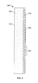
- Figure 4 is a diagram of an exemplary pattern 400 that may be induced to release coating 124, and/or used with setter 102, and/or heat extractor 122 (each shown in Figure 1 ).
- Figure 5 is a diagram of an alternative pattern 500 that may be applied/used to/with these same elements. More specifically, in an exemplary embodiment and as illustrated in both Figures 4 and 5 , dark dots and/or lines represent portions 402 and 502 that are raised or elongated with respect to substantially planar and/or recessed portions 404 and 504. In an alternative embodiment, the dark dots and/or lines may represent substantially planar and/or recessed portions 402 and 502 relative to raised or elevated portions 404 and 504.
- the patterns 400 and 500 When patterns 400 and 500 are imparted to a surface of melt 126, such as top surface 128, the patterns 400 and 500 facilitate inducing nucleation at raised portions 402 and 502 by reducing the temperature of melt 126 at predetermined portions 402 and 502. Moreover, the portions 402 and 502 facilitate reducing the temperature of melt 126 by modifying the heat exchange properties in such locations. For example, when a heat extractor 122, including pattern 400, is positioned in close proximity to melt 126 such that portions 402 are positioned closer to or against melt 126 than portions 404, heat transfer between melt 126 and portions 402 is faster than heat transfer between melt 128 and portions 404. As heat transfers from melt 126 continues, the temperature at which melt 126 will begin nucleation is reached more quickly at the locations of melt 126 that are closest to portions 402 than at the locations of melt 126 that are closest to portions 404.
- a pattern such as pattern 400 or pattern 500 (shown in Figures 4 and 5 , respectively), may be used to apply a thermal gradient to melt 126 (shown in Figure 1 ).
- applying a thermal gradient facilitates reducing the temperature of melt 126 at predetermined locations 142. Reducing the temperature of melt 126 at predetermined locations 142 facilitates inducing nucleation in a more controlled manner.
- the above-described embodiments of methods and apparatus for fabricating a semiconductor wafer facilitate inducing nucleation at predetermined locations of a semiconductor melt.
- Inducing nucleation at predetermined locations within a semiconductor melt facilitates a more ordered nucleation, thereby increasing the quality of the wafers.
- Increased wafer quality facilitates increasing performance of the associated component including the wafer, i.e., the associated solar cell, by causing a substantially uniform distribution across the wafer while maintaining low cost.
- inducing nucleation at predetermined locations within a semiconductor melt facilitates growth of larger grains and/or a more columnar grain structure. Such a grain structure facilitates improving the electrical qualities of a semiconductor wafer, thereby increasing the efficiency of the solar cells having such semiconductor wafers.
Landscapes
- Chemical & Material Sciences (AREA)
- Engineering & Computer Science (AREA)
- Crystallography & Structural Chemistry (AREA)
- Materials Engineering (AREA)
- Metallurgy (AREA)
- Organic Chemistry (AREA)
- Photovoltaic Devices (AREA)
- Liquid Deposition Of Substances Of Which Semiconductor Devices Are Composed (AREA)
- Recrystallisation Techniques (AREA)
- Crystals, And After-Treatments Of Crystals (AREA)
Abstract
Description
- This invention relates generally to semiconductor sheets, and more specifically to methods and apparatus for manufacturing semiconductor wafers.
- Wafers formed of semiconductor materials are used in a variety of applications and most, if not all, such applications require an increasing number of such wafers. For example, the use of photovoltaic systems has become more common and of greater importance in the production of energy. Moreover, the use of photovoltaic systems is therefore expected to increase dramatically. At least some known photovoltaic systems use a semiconductor substrate, such as a substrate consisting of single crystal or poly-crystalline silicon. However, the use of photovoltaic technology may be limited by the cost of semiconductor wafers used in the photovoltaic systems.
- A wide variety of fabrication methods exist for producing semiconductor wafers. In at least one known fabrication method, poly-crystalline silicon wafers for use in solar cells are produced by melting a high-purity material in an inert atmosphere. In such a method, the resulting silicon melt is cooled to form a polycrystalline ingot which is then sliced with a wire saw or an inner diameter blade to produce wafers of a desired thickness and size.
- Other known fabrication methods of producing wafers rely on a random nucleation of crystals in the semiconductor material melt. Such methods generally produce low-cost wafers, but because control of the nucleation of the semiconductor material melt is difficult, such wafers are generally of a low quality. Use of low-quality wafers within photovoltaic cells generally lowers the efficiency of such cells. Moreover, because the control of the nucleation of the semiconductor material is difficult, the costs of manufacturing such wafers is generally higher than with other fabrication methods.
- In one aspect according to the present invention, a method for fabricating a semiconductor wafer is provided. The method includes applying a layer of semiconductor material across a portion of a setter material, introducing the setter material and the semiconductor material to a predetermined thermal gradient to form a melt, wherein the thermal gradient includes a predetermined nucleation and growth region, and forming at least one local cold spot in the nucleation and growth region to facilitate inducing crystal nucleation at the at least one desired location.
- In another aspect, a method for fabricating a wafer is provided. The method includes providing a setter, applying a release coating across a top surface of the setter, depositing a semiconductor material across a top surface of the release coating, forming a melt by introducing the release coating and the semiconductor material to a predetermined temperature gradient, and applying a thermal pattern to the melt to induce nucleation in at least one desired location.
- In another aspect, a semiconductor wafer is provided. The wafer includes a body having a substantially uniform crystallization defined by a predetermined pattern. The wafer is fabricated by applying a release coating across a top surface of a setter material, applying at least one layer of at least one semiconductor material across a top surface of the release coating, introducing the setter material, release coating, and the at least one semiconductor material to a predetermined temperature gradient to form a melt across the at least one semiconductor material layer, and forming at least one local cold spot according to the predetermined pattern.
- Various aspects and embodiments of the present invention will now be described in connection with the accompanying drawings, in which:
-
Figure 1 is a schematic diagram of an exemplary fabrication apparatus that may be used to manufacture semiconductor wafers; -
Figure 2 is a flow chart illustrating an exemplary method of fabricating a semiconductor wafer using the fabrication apparatus shown inFigure 1 ; -
Figure 3 is an illustration of an exemplary heat extractor that may be used with the apparatus shown inFigure 1 ; -
Figure 4 is a diagram of an exemplary pattern that may be used with the apparatus shown inFigure 1 using the method shown inFigure 2 ; and -
Figure 5 is a diagram of an alternative pattern that may be used with the apparatus shown inFigure 1 using the method shown inFigure 2 . - Currently, silicon is one of the most commonly used semiconductor materials, also referred to as feedstock, used in the fabrication of semiconductor wafers. Accordingly, as used herein, the terms "semiconductor" and "semiconductor materials" refer to silicon based components and silicon materials. However, as will be readily appreciated by one of ordinary skill in the art, other semiconductor materials in addition to the silicon materials and/or including non-silicon materials can be fabricated using the apparatus and methods described herein. Although only the use of silicon powder feedstock is described herein for use in fabricating a silicon sheet, liquid silicon feedstock and/or crystallized silicon feedstock may be used without deviating from the present invention.
-
Figure 1 is a schematic diagram of anexemplary fabrication apparatus 100 that may be used to manufacture semiconductor wafers. In the exemplary embodiment,fabrication apparatus 100 is a controlled atmosphere furnace that includes a plurality of zones able to operate with different temperature conditions.Fabrication apparatus 100, in the exemplary embodiment, includes a plurality ofrollers 104, ahopper 108, adoctor blade 110, and a heating/cooling region 116. Moreover, in the exemplary embodiment,setter 102 is propelled byrollers 104 to enablesetter 102 to be moved under ahopper 108 that deposits a desired quantity ofsemiconductor material 112, and any desired additives, across a portion of atop surface 118 ofsetter 102. More specifically, in the exemplary embodiment, at least one layer ofsemiconductor material 112 is deposited ontop surface 118. In an alternative embodiment, a second hopper (not shown) may be used to dispenseadditional semiconductor material 112 across a portion oftop surface 118 and/or across a layer of material previously deposited onsetter 102. The portion ofsetter 102 containingsemiconductor material 112 is then moved beneath adoctor blade 110 and into heating/cooling region 116. - In the exemplary embodiment, heating/
cooling region 116 includes at least onethermal treatment device 114.Thermal treatment device 114 provides heat energy to heating/cooling region 116 and, thus, induces heat to anything placed withinregion 116. Any heat source may be used that enablesfabrication apparatus 100 to function as described herein. In the exemplary embodiment, heating/cooling region 116 also includes at least oneheat extractor 122.Heat extractor 122 removes heat from an object positioned within heating/cooling region 116. - An inert atmosphere is preferably maintained within an interior of
fabrication apparatus 100. More specifically, in the exemplary embodiment, the interior offabrication apparatus 100 is sealed to facilitate preventing the inert materials from escaping from thefabrication apparatus 100 and/or to prevent the influx of contaminants from external tofabrication apparatus 100. -
Figure 2 is a flow chart illustrating anexemplary method 200 of fabricating asemiconductor wafer 144 using fabrication apparatus 100 (shown inFigure 1 ). Referring to bothFigures 1 and2 , when fabricating asemiconductor wafer 144, asetter 102 is initially selected 201. More specifically, the shape of thesetter 102 selected determines the shape of the finishedsemiconductor wafer 144 produced. Accordingly,setter 102 may provide, for example and without limitation, substantially square wafers, substantially circular wafers, and/or substantially rectangular wafers.Setter 102 may include one or more recesses (not shown) that have a predetermined shape and/or a predetermined topography that imparts a pattern (not shown inFigures 1 and2 ) on material layers during the fabrication process. For example, the recesses may be organized into a series of peaks and valleys. In the exemplary embodiment,setter 102 includes one or more recesses defined on each of a first surface (not shown) and an opposite second surface (not shown). Providing recesses on both the first and second surfaces allowssetter 102 to be moved through a furnace, such asapparatus 100, with either side facing upward and with either side against thesetter 102. - A
release coating 124 is applied 202 across settertop surface 118 to enable thatsetter 102 to easily separate from the finishedsemiconductor wafer 144. In one embodiment, therelease coating 124 is silicon nitride (Si3N4). Alternative embodiments may use silicon dioxide (SiO2) or silicon carbide (SiC) as a release agent. In other alternative embodiments, any other ingredient can be used as a release agent that enableswafers 144 to be produced as described herein. More specifically, in the exemplary embodiment, a liquid slurry containing therelease coating 124 is applied tosetter 102. Therelease coating 124 may be applied to setter 102 using known application means including, but not limited to, a painting process and/or a spraying process. In one embodiment, therelease coating 124 is applied tosetter 102 in a predetermined pattern. In another embodiment,release coating 124 is applied in a predetermined thickness gradient. - At least one
semiconductor material 112 is then deposited 203 across therelease coating 124. In the exemplary embodiment,semiconductor material 112 is deposited 203 after therelease coating 124 has dried. Moreover, in the exemplary embodiment,semiconductor material 112 is deposited in a predetermined amount from ahopper 108, as described above. In one embodiment,semiconductor material 112 is deposited overrelease coating 124 with a substantially constant thickness. In another embodiment,semiconductor material 112 is deposited overrelease coating 124 in a predetermined pattern and/or with a predetermined thickness gradient. - In the exemplary embodiment,
setter 102, includingrelease coating 124 andsemiconductor material 112, is then moved 204 through heating/cooling region 116.Heat sources 114 andheat extractor 122 within heating/region 116 induce a desiredthermal profile 140 tomaterial 112 andcoating 124. In the exemplary embodiment,thermal profile 140 includes a plurality of regions having varying temperatures and wherein thesemiconductor material 112 undergoes physical changes. For example, apreheat region 130 occurs aftersetter 102, includingrelease coating 124 andsemiconductor material 112 is passed underdoctor blade 110. Amelt region 132 is then introduced tocoating 124 andmaterial 112, such that withinmelt region 132, the temperature exceeds, by a predetermined amount, the melting temperature ofsemiconductor material 112. As a result, withinmelt region 132 at least atop surface 128 ofsemiconductor material 112 forms amelt 126.Setter 102 then enterscrystallization region 134, wherein a liquid layer (not shown) and crystallized layer (not shown) coexist. In the exemplary embodiment, the temperature incrystallization region 134 is reduced in a predetermined manner to facilitate crystallization ofmelt 126. The temperature may be modified by positioning and/orrepositioning heat sources 114 and/orheat extractor 122.Thermal profile 142 also includes acooling region 136, wherein the crystallizedsemiconductor material 112 is further cooled. Finally, the cooledwafers 144 are unloaded fromapparatus 100 in a wafer unloadregion 138. - While in
crystallization region 134, a predetermined thermal pattern is applied 205 to melt 126 to induce nucleation ofsemiconductor material 112 in a predetermined location or locations. In the exemplary embodiment, nucleation is induced by changing the heat transfer properties ofmelt 126, such that a localcold spot 142 is formed on asurface 128 ofmelt 126. Inducing nucleation at a localcold spot 142 facilitates an orderly crystal formation withinmelt 126. The heat transfer properties may be changed using a variety of methods. In one embodiment,release coating 124 may be applied tosetter 102 in a predetermined pattern (not shown inFigures 1 and2 ). In another embodiment,release coating 124 may be applied tosetter 102 in a predetermined thickness gradient. In another embodiment, the thermal pattern is applied 205 usingheat extractor 122, as described below. -
Figure 3 is an illustration of anexemplary heat extractor 122 that may be used with apparatus 100 (shown inFigure 1 ). More specifically, in one embodiment,heat extractor 122 includes apattern 306, a cooledlayer 302, and aninsulation layer 304. In an alternative embodiment, cooledlayer 302 andinsulation layer 304 are composed of substantially different materials and are positioned such that there is no contact betweenlayers insulation layer 304 includes a plurality of holes such thatinsulation layer 304 acts as a patterned mask between cooledlayer 302 and melt 126. Moreover, in one embodiment, cooledlayer 302 consists substantially of a metal. In an alternative embodiment, cooledlayer 302 consists substantially of graphite. In the exemplary embodiment,heat extractor 122 is positioned withinapparatus 100 such that afirst surface 308 ofheat extractor 122 is closer to melt 126 than an oppositesecond surface 310 ofheat extractor 122. In oneembodiment heat extractor 122 is positioned in close proximity to melt 126. In such an embodiment,heat extractor 122 is fabricated substantially from a refractory metal and/or a ceramic material. Alternatively,heat extractor 122 may be fabricated from any material that allowsheat extractor 122 to function as described herein. Alternatively, in the embodiment described above, in whichheat extractor 122 is positioned in contact withmelt 126,heat extractor 122 is fabricated from a material or combination of materials that facilitate preventingmelt 126 from adhering toheat extractor 122. Further,heat extractor 122 is fabricated from a material or combination of materials that enablesheat extractor 122 to withstand the high temperatures used withinapparatus 100. - During operation,
heat extractor 122 is used incrystallization region 134 to apply a thermal gradient to melt 126 (shown inFigure 1 ). In one embodiment,heat extractor 122 is positioned in close proximity to melt 126. More specifically, in such an embodiment,heat extractor 122 is positioned approximately between 0.5 and 15.0 millimeters (mm) and, more specifically, between approximately 1.0 and 10.0 mm fromtop surface 128 ofmelt 126. In another embodiment,heat extractor 122 is positioned against melttop surface 128.Heat extractor 122 may include, but is not limited to including, pattern and/or substantially planar surface. -
Figure 4 is a diagram of anexemplary pattern 400 that may be induced to release coating 124, and/or used withsetter 102, and/or heat extractor 122 (each shown inFigure 1 ).Figure 5 is a diagram of analternative pattern 500 that may be applied/used to/with these same elements. More specifically, in an exemplary embodiment and as illustrated in bothFigures 4 and 5 , dark dots and/or lines representportions portions portions elevated portions patterns melt 126, such astop surface 128, thepatterns portions melt 126 atpredetermined portions portions melt 126 by modifying the heat exchange properties in such locations. For example, when aheat extractor 122, includingpattern 400, is positioned in close proximity to melt 126 such thatportions 402 are positioned closer to or againstmelt 126 thanportions 404, heat transfer betweenmelt 126 andportions 402 is faster than heat transfer betweenmelt 128 andportions 404. As heat transfers frommelt 126 continues, the temperature at which melt 126 will begin nucleation is reached more quickly at the locations ofmelt 126 that are closest toportions 402 than at the locations ofmelt 126 that are closest toportions 404. - During operation, a pattern, such as
pattern 400 or pattern 500 (shown inFigures 4 and 5 , respectively), may be used to apply a thermal gradient to melt 126 (shown inFigure 1 ). In the exemplary embodiment, and as described above, applying a thermal gradient facilitates reducing the temperature ofmelt 126 atpredetermined locations 142. Reducing the temperature ofmelt 126 atpredetermined locations 142 facilitates inducing nucleation in a more controlled manner. - The above-described embodiments of methods and apparatus for fabricating a semiconductor wafer facilitate inducing nucleation at predetermined locations of a semiconductor melt. Inducing nucleation at predetermined locations within a semiconductor melt facilitates a more ordered nucleation, thereby increasing the quality of the wafers. Increased wafer quality facilitates increasing performance of the associated component including the wafer, i.e., the associated solar cell, by causing a substantially uniform distribution across the wafer while maintaining low cost. Moreover, inducing nucleation at predetermined locations within a semiconductor melt facilitates growth of larger grains and/or a more columnar grain structure. Such a grain structure facilitates improving the electrical qualities of a semiconductor wafer, thereby increasing the efficiency of the solar cells having such semiconductor wafers.
- Exemplary embodiments of methods and apparatus for fabricating a semiconductor wafer are described above in detail. The methods and apparatus are not limited to the specific embodiments described herein, but rather, components of the methods and apparatus may be utilized independently and separately from the other components described herein.
- While the invention has been described in terms of various specific embodiments, those skilled in the art will recognize that the invention can be practiced with modification within the spirit and scope of the claims.
- Various aspects and embodiments of the present invention are now defined by the following numbered clauses:
- 1. A method for fabricating a semiconductor wafer, said method comprising:
- applying a layer of semiconductor material across a portion of a setter material;
- introducing the setter material and the semiconductor material to a predetermined thermal gradient, including a predetermined nucleation and growth region, to form a melt; and
- forming at least one local cold spot in the nucleation and growth region to facilitate inducing crystal nucleation at the at least one desired location.
- 2. A method in accordance with Clause 1 further comprising applying a release coating layer to the setter material such that the release coating is between the setter material and the semiconductor material layer, wherein the release coating is applied with at least one of a predetermined pattern and a thickness gradient.
- 3. A method in accordance with any preceding Clause wherein applying a layer of semiconductor material comprises applying the semiconductor material across a release coating applied across the setter material, wherein the setter material is formed with a predetermined pattern.
- 4. A method in accordance with any preceding Clause wherein forming at least one local cold spot comprises positioning a heat extractor at a predetermined distance from the melt.
- 5. A method in accordance with any preceding Clause wherein positioning a heat extractor at a predetermined distance from the melt comprises positioning a heat extractor formed with a pattern at a predetermined distance from the melt.
- 6. A method in accordance with any preceding Clause wherein forming at least one local cold spot comprises contacting the melt with at least a portion of a heat extractor.
- 7. A method in accordance with any preceding Clause wherein contacting the melt with at least a portion of a heat extractor comprises contacting the melt with at least a patterned portion of the heat extractor.
- 8. A method for fabricating a wafer, said method comprising:
- providing a setter;
- applying a release coating across a top surface of the setter;
- depositing a semiconductor material across a top surface of the release coating;
- forming a melt by introducing the release coating and the semiconductor material to a predetermined temperature gradient; and
- applying a thermal pattern to the melt to induce nucleation in at least one desired location.
- 9. A method in accordance with Clause 8 wherein applying a release coating comprises applying a release coating across a top surface of the setter, wherein the release coating is applied with at least one of a predetermined pattern and a thickness gradient.
- 10. A method in accordance with Clause 8 or 9 wherein depositing a semiconductor material comprises depositing the semiconductor material across a top surface of a release coating, wherein the setter includes a predetermined pattern.
- 11. A method in accordance with any of Clauses 8 to 10 wherein applying a thermal pattern to the melt comprises positioning a heat extractor in close proximity to the melt.
- 12. A method in accordance with any of Clauses 8 to 11 wherein positioning a heat extractor in close proximity to the melt comprises positioning a heat extractor formed with a pattern in close proximity to the melt.
- 13. A method in accordance with any of Clauses 8 to 12 wherein applying a thermal pattern to the melt comprises placing a heat extractor in contact with an outer surface of the melt.
- 14. A method in accordance with any of Clauses 8 to 13 wherein placing a heat extractor in contact with a surface of the melt comprises placing a patterned portion of the heat extractor in contact with the outer surface of the melt.
- 15. A semiconductor wafer comprising a body having a substantially uniform crystallization defined by a predetermined pattern, said semiconductor wafer fabricated by:
- applying a release coating across a top surface of a setter material;
- applying at least one layer of at least one semiconductor material across a top surface of the release coating;
- introducing the setter material, release coating, and the at least one semiconductor material to a predetermined temperature gradient to form a melt across the at least one semiconductor material layer; and
- forming at least one local cold spot according to the predetermined pattern.
- 16. A semiconductor wafer in accordance with Clause 15 wherein the release coating is applied with the predetermined pattern.
- 17. A semiconductor wafer in accordance with Clause 15 or 16 wherein the release coating is applied with a predetermined thickness gradient.
- 18. A semiconductor wafer in accordance with any of Clauses 15 to 17 wherein the setter material includes the predetermined pattern.
- 19. A semiconductor wafer in accordance with any of Clauses 15 to 18 wherein the predetermined pattern is applied to the melt by positioning a heat extractor at a predetermined distance from the melt, wherein the heat extractor includes at least one of the predetermined pattern and a substantially planar surface.
- 20. A semiconductor wafer in accordance with any of Clauses 15 to 19 wherein the predetermined pattern is applied to the melt by contacting the melt with at least a portion of a heat extractor, wherein the heat extractor includes at least one of the predetermined pattern and a substantially planar surface.
Claims (6)
- A semiconductor wafer (144) comprising a body having a substantially uniform crystallization defined by a predetermined pattern (306), said semiconductor wafer fabricated by:applying (202) a release coating (124) any preceding across a top surface (118) of a setter material (102);applying (203) at least one layer of at least one semiconductor material (112) across a top surface of the release coating;introducing (204) the setter material, release coating, and the at least one semiconductor material to a predetermined temperature gradient to form a melt (126) across the at least one semiconductor material layer; andforming (205) at least one local cold spot (142) according to the predetermined pattern.
- A semiconductor wafer (144) in accordance with Claim 1 wherein the release coating (124) is applied (202) with the predetermined pattern (306).
- A semiconductor wafer (144) in accordance with any preceding Claim wherein the release coating (124) is applied (202) with a predetermined thickness gradient.
- A semiconductor wafer (144) in accordance with any preceding Claim wherein the setter material (102) includes the predetermined pattern (306).
- A semiconductor wafer (144) in accordance with any preceding Claim wherein the predetermined pattern (306) is applied to the melt (126) by positioning a heat extractor (122) at a predetermined distance from the melt, wherein the heat extractor includes at least one of the predetermined pattern and a substantially planar surface.
- A semiconductor wafer (144) in accordance with any preceding Claim wherein the predetermined pattern (306) is applied to the melt (126) by contacting the melt with at least a portion of a heat extractor (122), wherein the heat extractor includes at least one of the predetermined pattern and a substantially planar surface.
Applications Claiming Priority (1)
| Application Number | Priority Date | Filing Date | Title |
|---|---|---|---|
| US12/026,586 US8334194B2 (en) | 2008-02-06 | 2008-02-06 | Methods and apparatus for manufacturing semiconductor wafers |
Publications (1)
| Publication Number | Publication Date |
|---|---|
| EP2088617A1 true EP2088617A1 (en) | 2009-08-12 |
Family
ID=40622284
Family Applications (1)
| Application Number | Title | Priority Date | Filing Date |
|---|---|---|---|
| EP09151743A Withdrawn EP2088617A1 (en) | 2008-02-06 | 2009-01-30 | Methods and apparatus for manufacturing semiconductor wafers |
Country Status (2)
| Country | Link |
|---|---|
| US (1) | US8334194B2 (en) |
| EP (1) | EP2088617A1 (en) |
Citations (2)
| Publication number | Priority date | Publication date | Assignee | Title |
|---|---|---|---|---|
| EP0591949A1 (en) * | 1992-10-09 | 1994-04-13 | ASTROPOWER Inc. | Improved columnar-grained polycrystalline silicon solar cell and process of manufacture |
| WO2004012257A1 (en) * | 2002-07-31 | 2004-02-05 | Astropower, Inc. | Method and apparatus for manufacturing net shape semiconductor wafers |
Family Cites Families (10)
| Publication number | Priority date | Publication date | Assignee | Title |
|---|---|---|---|---|
| US4050507A (en) | 1975-06-27 | 1977-09-27 | International Business Machines Corporation | Method for customizing nucleate boiling heat transfer from electronic units immersed in dielectric coolant |
| US4330363A (en) | 1980-08-28 | 1982-05-18 | Xerox Corporation | Thermal gradient control for enhanced laser induced crystallization of predefined semiconductor areas |
| US4389904A (en) | 1981-03-23 | 1983-06-28 | The United States Of America As Represented By The Administrator Of The National Aeronautics And Space Administration | Method and apparatus for supercooling and solidifying substances |
| CA1239706A (en) | 1984-11-26 | 1988-07-26 | Hisao Hayashi | Method of forming a thin semiconductor film |
| US5893948A (en) | 1996-04-05 | 1999-04-13 | Xerox Corporation | Method for forming single silicon crystals using nucleation sites |
| US6555449B1 (en) | 1996-05-28 | 2003-04-29 | Trustees Of Columbia University In The City Of New York | Methods for producing uniform large-grained and grain boundary location manipulated polycrystalline thin film semiconductors using sequential lateral solidfication |
| KR100234895B1 (en) | 1997-05-12 | 1999-12-15 | 구본준 | Crystalizing method of amorphorous silicon |
| KR100327087B1 (en) | 1999-06-28 | 2002-03-13 | 구본준, 론 위라하디락사 | Laser annealing method |
| US6451631B1 (en) | 2000-08-10 | 2002-09-17 | Hitachi America, Ltd. | Thin film crystal growth by laser annealing |
| JP2008546203A (en) * | 2005-06-01 | 2008-12-18 | マットソン テクノロジー インコーポレイテッド | A method to optimize the heat balance during pulsed heat treatment |
-
2008
- 2008-02-06 US US12/026,586 patent/US8334194B2/en not_active Expired - Fee Related
-
2009
- 2009-01-30 EP EP09151743A patent/EP2088617A1/en not_active Withdrawn
Patent Citations (2)
| Publication number | Priority date | Publication date | Assignee | Title |
|---|---|---|---|---|
| EP0591949A1 (en) * | 1992-10-09 | 1994-04-13 | ASTROPOWER Inc. | Improved columnar-grained polycrystalline silicon solar cell and process of manufacture |
| WO2004012257A1 (en) * | 2002-07-31 | 2004-02-05 | Astropower, Inc. | Method and apparatus for manufacturing net shape semiconductor wafers |
Non-Patent Citations (1)
| Title |
|---|
| HAHN G ET AL: "TOPICAL REVIEW; New crystalline silicon ribbon materials for photovoltaics; Topical Review", JOURNAL OF PHYSICS: CONDENSED MATTER, INSTITUTE OF PHYSICS PUBLISHING, BRISTOL, GB, vol. 16, no. 50, 22 December 2004 (2004-12-22), pages R1615 - R1648, XP020060559, ISSN: 0953-8984 * |
Also Published As
| Publication number | Publication date |
|---|---|
| US8334194B2 (en) | 2012-12-18 |
| US20090194849A1 (en) | 2009-08-06 |
Similar Documents
| Publication | Publication Date | Title |
|---|---|---|
| CN101503820B (en) | Methods and apparatus for manufacturing semiconductor wafers | |
| US6946029B2 (en) | Sheet manufacturing method, sheet, sheet manufacturing apparatus, and solar cell | |
| KR101527139B1 (en) | Recrystallization of semiconductor wafers in a thin film capsule and related processes | |
| US20060043367A1 (en) | Semiconductor device and method of fabricating a low temperature poly-silicon layer | |
| CN114075699B (en) | Double-layer composite silicon carbide substrate and preparation method thereof | |
| TWI545234B (en) | Crucible and method for the production of a (near) monocrystalline semiconductor ingot | |
| CN102648310A (en) | High throughput recrystallization of semiconducting materials | |
| JP7145763B2 (en) | Crucible for silicon ingot growth with patterned protrusion structure layer | |
| WO2014056157A1 (en) | Polycrystalline silicon ingot, method for producing the same, and crucible | |
| WO2007136420A2 (en) | Apparatus for fabricating large-surface area polycrystalline silicon sheets for solar cell application | |
| KR100942185B1 (en) | Silicon Ingot Growth Method | |
| US8334194B2 (en) | Methods and apparatus for manufacturing semiconductor wafers | |
| TWI595124B (en) | Manufacturing method of polysilicon ingot | |
| CN101575732A (en) | Semiconductor sheets and methods of fabricating the same | |
| US6951585B2 (en) | Liquid-phase growth method and liquid-phase growth apparatus | |
| EP0304337B1 (en) | Hybrid substrate | |
| KR20140006940A (en) | Article and method for forming large grain polycrystalline silicon films | |
| KR101431457B1 (en) | A method for manufacturing of crucible protecting layer | |
| WO2011156976A1 (en) | Method for polycrystalline silicon ingot casting | |
| WO2018024830A1 (en) | Crucible for crystallization of molten silicon, process for its manufacture and use thereof | |
| EP2991122A1 (en) | Heat treatment method for compound semiconductor precursor layer | |
| KR100697384B1 (en) | Silicon crystallization method | |
| US20160141442A1 (en) | Use of silicon nitride as a substrate and a coating material for the rapid solidification of silicon | |
| Lee et al. | Precise control of nucleation and growth in lead zirconate titanate thin films by scanning rapid thermal annealing | |
| Rangarajan et al. | Characterization of Green Laser Crystallized GeSi Thin Films |
Legal Events
| Date | Code | Title | Description |
|---|---|---|---|
| PUAI | Public reference made under article 153(3) epc to a published international application that has entered the european phase |
Free format text: ORIGINAL CODE: 0009012 |
|
| AK | Designated contracting states |
Kind code of ref document: A1 Designated state(s): AT BE BG CH CY CZ DE DK EE ES FI FR GB GR HR HU IE IS IT LI LT LU LV MC MK MT NL NO PL PT RO SE SI SK TR |
|
| AX | Request for extension of the european patent |
Extension state: AL BA RS |
|
| 17P | Request for examination filed |
Effective date: 20100212 |
|
| AKX | Designation fees paid |
Designated state(s): DE ES IT |
|
| 17Q | First examination report despatched |
Effective date: 20100401 |
|
| RAP1 | Party data changed (applicant data changed or rights of an application transferred) |
Owner name: MOTECH AMERICAS, LLC |
|
| STAA | Information on the status of an ep patent application or granted ep patent |
Free format text: STATUS: THE APPLICATION IS DEEMED TO BE WITHDRAWN |
|
| 18D | Application deemed to be withdrawn |
Effective date: 20101012 |