EP2086221A1 - Imaging device holding structure and imaging device - Google Patents
Imaging device holding structure and imaging device Download PDFInfo
- Publication number
- EP2086221A1 EP2086221A1 EP07829711A EP07829711A EP2086221A1 EP 2086221 A1 EP2086221 A1 EP 2086221A1 EP 07829711 A EP07829711 A EP 07829711A EP 07829711 A EP07829711 A EP 07829711A EP 2086221 A1 EP2086221 A1 EP 2086221A1
- Authority
- EP
- European Patent Office
- Prior art keywords
- image pickup
- wiring board
- pickup device
- holding member
- pickup element
- Prior art date
- Legal status (The legal status is an assumption and is not a legal conclusion. Google has not performed a legal analysis and makes no representation as to the accuracy of the status listed.)
- Granted
Links
Images




Classifications
-
- H—ELECTRICITY
- H04—ELECTRIC COMMUNICATION TECHNIQUE
- H04N—PICTORIAL COMMUNICATION, e.g. TELEVISION
- H04N23/00—Cameras or camera modules comprising electronic image sensors; Control thereof
- H04N23/50—Constructional details
- H04N23/54—Mounting of pick-up tubes, electronic image sensors, deviation or focusing coils
-
- H—ELECTRICITY
- H04—ELECTRIC COMMUNICATION TECHNIQUE
- H04N—PICTORIAL COMMUNICATION, e.g. TELEVISION
- H04N23/00—Cameras or camera modules comprising electronic image sensors; Control thereof
- H04N23/50—Constructional details
- H04N23/51—Housings
Definitions
- the present invention relates to a holding structure for an image pickup device with a so-called back-incident type image pickup element, and an image pickup device.
- This semiconductor energy detector is provided with a BT-CCD (Back-Thinned CCD) for which a part of the semiconductor substrate is thinned on the opposite side to the image pickup unit and which is capable of imaging various types of energy beams including ultraviolet rays, soft X-rays, and electron beams at a high sensitivity and a package electrically connected with the BT-CCD by wire bonding.
- the back-incident type image pickup element is used as, for example, a photodetecting section of a telescope for astronomical observation.
- the image pickup device when used as, for example, a photodetecting section of a telescope for astronomical observation, a buttable arrangement structure has been adopted for increasing the resolution of the photodetecting section, where a plurality of image pickup devices are disposed in a matrix arrangement on an installation body such as a cold plate.
- the buttable arrangement structure for reducing a region (non-sensitive region) where imaging cannot be performed, to approximate (almost equalize) a wiring board that carries an image pickup element to the area of the image pickup element as much as possible and arrange the image pickup elements on the installation body at a high density.
- an object of the present invention is to provide a holding structure for an image pickup device that allows preventing damage to the peripheral edge portion of an image pickup element, and an image pickup device.
- a holding structure for an image pickup device includes: an image pickup device having an image pickup element that picks up an optical image made incident from one surface side by an image pickup unit being at the other surface side and a wiring board provided at the other surface side of the optical image pickup element; and a holding member freely attachably and detachably attached to a side face of the optical image wiring board so as to surround the optical image pickup element, the holding member holding the optical image wiring board, wherein a first engaging portion is formed at each of the opposing side faces in the optical image wiring board, and a second engaging portion to be engaged with the first engaging portion is formed at the holding member.
- the holding member that holds the wiring board is freely attachably and detachably attached to the side face of the wiring board.
- the first engaging portion is formed, and the first engaging portion and the second engaging portion formed at the holding member are fitted together.
- the holding member is thus freely attachably and detachably attached to the side face of the wiring board, handling of the image pickup device is facilitated, and an unnecessary impact to be applied to the image pickup device can also be suppressed. Accordingly, by the holding structure for an image pickup device according to the present invention, it becomes possible to prevent damage to the peripheral edge portion of the image pickup element.
- the first engaging portion is recessed and the second engaging portion is projected, and the first engaging portion and the second engaging portion are fitted together.
- the holding member can be further suppressed from coming off.
- the first engaging portion is thus recessed, it also becomes possible to arrange the image pickup devices at a further high density in the buttable arrangement structure of the image pickup devices without the obstruction by the engaging portions.
- first engaging portion may extend from one longitudinal end of the side face to the other longitudinal end, and the first engaging portion may be intermittently provided from one longitudinal end of the side face to the other longitudinal end.
- the wiring board is a laminate formed by laminating a plurality of substrates.
- the wiring board is a laminate formed by laminating a plurality of substrates.
- a part of the side face in the wiring board is recessed. That is, the engaging portion can be simply formed.
- the protecting member can inhibit an impact from being directly applied to the image pickup element, and makes it possible to prevent dust and dirt from adhering to the image pickup element.
- the protecting member includes a light transmitting region. In this case, even when the image pickup element is covered with the protecting member, an optical image can be made incident into the image pickup element from the light transmitting region.
- the image pickup device is an image pickup device that is held by a freely attachable and detachable holding member, including: an image pickup element that picks up an optical image made incident from one surface side by an image pickup unit being at the other surface side; and a wiring board provided at the other surface side of the image pickup element, wherein a first engaging portion for engaging with the holding member is formed at each of the opposing side faces in the wiring board.
- the first engaging portion for engaging with the holding member is formed at each of the opposing side faces in the wiring board. Therefore, when the holding member and the first engaging portion are engaged and the holding member is freely attachably and detachably attached to the side face of the wiring board, the following operational effects can be obtained. That is, it becomes possible, even when an impact is applied to the image pickup device during an inspection, delivery, etc., to relieve the impact to be applied to the wiring board and the image pickup element by the holding member while suppressing the holding member from coming off. Further, since the holding member is thus freely attachably and detachably attached to the side face of the wiring board, handling of the image pickup device is facilitated, and an unnecessary impact to be applied to the image pickup device can also be suppressed. Accordingly, by the image pickup device according to the present invention, it becomes possible to prevent damage to the peripheral edge portion of the image pickup element.
- 1 ⁇ image pickup device 11 ⁇ image pickup element, 12 ⁇ wiring board, 16 ⁇ CCD array (image pickup unit), 27, 27a, 27b ⁇ side face, 28 ⁇ to-be-fitted portion (first engaging portion), 51 ⁇ holding member, 53 ⁇ glass window (light transmitting region), 54 ⁇ fitting portion (second engaging portion), 55 ⁇ protecting member, 100 ⁇ holding structure for image pickup device.
- Fig. 1 is a perspective view showing an image pickup device included in a holding structure for an image pickup device according to one embodiment of the present invention
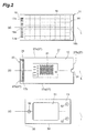
- Fig. 2(a) is a front view showing an image pickup element included in the image pickup device of Fig. 1
- Fig. 2(b) is a front view showing a wiring board included in the image pickup device of Fig. 1
- Fig. 2(c) is a front view showing a pin base included in the image pickup device of Fig. 1
- the image pickup device 1 has an image pickup element 11 that performs imaging, a wiring board 12 electrically connected to the image pickup element 11, and a pin base 13 used for installation of the image pickup device 1.
- the image pickup element 11 is a Back-Thinned CCD (BT-CCD) having a thickness of approximately 200 ⁇ m.
- the image pickup element 11 has a light-incident surface S at its back surface (one surface) side.
- a detecting region 14 that detects an optical image made incident from the light-incident surface S and a first bonding pad region 15 to serve as an output terminal of the detecting region 14 are respectively provided.
- a CCD array (image pickup unit) 16 where CCDs are arranged in, for example, a 9x7 matrix, and in the first bonding pad region 15, provided is a first bonding pad 17a electrically connected with the CCD array 16 via a predetermined pattern of aluminum wiring.
- the first bonding pads 17a are arranged in a line along one end portion of the image pickup element 11.
- positional alignment marks 18a, 18b are respectively provided so as to pass through a center line L of the image pickup element 11.
- the positional alignment marks 18a, 18b are formed simultaneously with the above-described aluminum wiring by, for example, sputtering of aluminum, and used as positional references that indicate the center line L of the image pickup element 11.
- the wiring board 12 shows a rectangular shape as a plane shape observed from its thickness direction, and is, for example, a laminate that is constructed by laminating and sintering green sheets (substrates).
- the area of the wiring board 12 is approximated to that of the image pickup element 11 as much as possible so as to be almost the same area as that of the image pickup element 11.
- the wiring board 12 has a width that is larger than the width of the image pickup element 11 by approximately 50 ⁇ m (25 ⁇ m at one side).
- to-be-fitted portions 28 In side faces 27a, 27a at the long sides of the wiring board 12, respectively formed are recessed to-be-fitted portions (first engaging portions) 28, with which a holding member to be described later is fitted.
- the to-be-fitted portion 28 extends from one longitudinal end of the side faces 27a, 27a at the long side of the wiring board 12 to the other longitudinal end.
- the to-be-fitted portion 28 is formed by laminating and sintering in a manner of sandwiching a green sheet having a narrow width in the short-side direction with green sheets having wider widths. Thereby, the to-be-fitted portions 28 are formed simply and reliably.
- a slit portion 23 and a cutaway portion 24 are provided, respectively.
- the slit portion 23 is formed in an oblong shape along one end portion of the wiring board 12, and the cutaway portion 24 is formed in a semicircular shape at almost the center of the other end portion of the wiring board 12.
- the wiring board 12 is, while being positioned so that the first bonding pad region 15 and the positional alignment mark 18a (see Fig. 2(a) ) are exposed from the slit portion 23 and the positional alignment mark 18b (see Fig. 2(a) ) is exposed from the cutaway portion 24, firmly fixed to the front surface side of the image pickup element 11 by, for example, die-bonding.
- the wiring board 12 is attached with a ceramic lid portion 29 from the front surface side of the slit portion 23.
- the lid portion 29 By attaching the lid portion 29, the first bonding pads 17a and second bonding pads 17b are protected so as not to be externally exposed.
- Fig. 2(b) shows a state where the lid portion 29 has been detached.
- a lead terminal 21 electrically connected to the second bonding pad 17b and corresponding to each CCD of the CCD array 16 is disposed.
- the lead terminal 21 is, for example, connected with a flexible PCB (Printed Circuit Board), and is externally connector-connected via the flexible PCB.
- the pin base 13 is formed of, for example, aluminum nitride in a flat rectangular parallelepiped shape.
- the pin base 13 is formed at almost the center with a rectangular opening portion 31 to expose the lead terminals 21 of the wiring board 12.
- a threaded fitting pin 32 made of, for example, titanium onto which a nut 36 can be screwed.
- a total of three threaded fitting pins 32 are provided in a manner sandwiching the opening portion 31, that is, one at the center of one end side of the pin base 13 and one each at positions close to both corner portions of the other end side of the pin base 13.
- one side face 34 along the center line L of the image pickup element 11 and a corner portion 35 of one end side in the side face 34 serve as a positioning portion of the pin base 13.
- the threaded fitting pins 32 are attached at the front surface side of the pin base 13 so as to be centered based on relative distances from the side face 34 and the corner portion 35 and positioned at a high accuracy with respect to the positioning portion, respectively.
- the pin base 13 is accurately angularly aligned with respect to the image pickup element 11 by aligning, with the center line L, the line of the side face 34 when the pin base 13 is observed from the front surface side, and is accurately positionally aligned with respect to the image pickup element 11 based on relative distances between the positional alignment marks 18a and 18b (see Fig. 2(a) ) and the corner portion 35.
- the pin base 13 is firmly adhered to the front surface side of the wiring board 12 by, for example, a thermosetting resin.
- Fig. 3 is a front view showing a part of an image pickup device according to one embodiment of the present invention in a sectioned manner
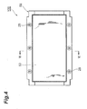
- Fig. 4 is a rear view showing the holding structure for an image pickup device shown in Fig. 3
- Fig. 5 is a side view showing a part of the holding structure for an image pickup device shown in Fig. 3 in a sectioned manner.
- the holding structure 100 for an image pickup device includes the above-mentioned image pickup device 1 and a holding member 51 that holds the image pickup device 1.
- the holding member 51 is made of, for example, aluminum, and has an almost frame shape such as to surround the image pickup element 11.
- the holding member 51 is constructed including a pair of long-side holding members 51a that abut against the side faces 27a of the long sides of the wiring board 12 and a pair of short-side holding members 51b that abut against side faces 27b of the short sides.
- screw holes 26 leading from both longitudinal end portions of the long-side holding member 51a to the short-side holding members 51b are formed.
- the long-side holding member 51a and the short-side holding member 51b are fixed to each other by attachable and detachable screws 22. These make the holding member 51 freely attachable and detachable with respect to the image pickup element 1.
- a protecting member 55 is freely attachably and detachably fixed by a screw 25 (see Fig. 4 ).
- the protecting member 55 is laminated to the light-incident surface S side of the holding member 51.
- the protecting member 55 shows, when this is observed from the light-incident surface S side, an almost rectangular shape corresponding to an outer edge of the holding member 51.
- the protecting member 55 covers the light-incident surface S of the image pickup element 11 to protect the light-incident surface S. Also, as shown in Fig.
- the protecting member 55 there provided between an inner surface of the protecting member 55 and the side face 27 of the wiring board 12 is a gap D, and the gap prevents the protecting member 55 from contacting with the image pickup element 11 on the wiring board 12 to damage the image pickup element 11.
- the protecting member 55 is provided with a glass window portion (light transmitting region) 53 having optical transparency and made of, for example, glass.
- the to-be-fitted portion 28 has a depth of, for example, approximately 700 ⁇ m and has a recessed form that is recessed toward the wiring board 12, and a bottom portion of the to-be-fitted portion 28 is formed so as to be located at the center in the thickness direction of the wiring board 12.
- the to-be-fitted portion 28 is a groove such as to be located, in the side face 27a of the long side of the wiring board 12, at the center in the thickness direction thereof. This allows suppressing a so-called chipping phenomenon where both end portions in the thickness direction of the wiring board 12 in the side face 27a of the long side of the wiring board 12, that is, parts to construct side walls of the recessed to-be-fitted portion 28, chip due to impact.
- the holding member 51 has a fitting portion (second engaging portion) 54 to be fitted with the to-be-fitted portion 28.
- a fitting portion (second engaging portion) 54 to be fitted with the to-be-fitted portion 28.
- the fitting portion 54 so as to correspond to the to-be-fitted portion 28, extends from one longitudinal end of the long-side holding member 51 a to the other longitudinal end.
- the first engaging portion is provided as the to-be-fitted portion 28 extending from one longitudinal end to the other longitudinal end at the side face 27a of the long side of the wiring board 12, as another example, there is also a case where, as another example, as shown in Fig. 8(b) , the first engaging portion is provided as a to-be-fitted portion 28b that is intermittently provided from one longitudinal end to the other longitudinal end.
- the to-be-fitted portion can be simply formed by, for example, laminating green sheets.
- a fitting portion of the holding member is, so as to correspond to the to-be-fitted portion 28b, intermittently provided from one longitudinal end of the long-side holding member to the other longitudinal end.
- the first engaging portion may even be partially provided at the side face of the long side of the wiring board.
- a fitting structure where the to-be-fitted portion is formed in a V-shape may of course be provided.
- the holding structure 100 for an image pickup device When the holding structure 100 for an image pickup device is assembled, first, the wiring board 12 is prepared, the short-side holding members 51 b are respectively attached to the side faces 27b of the short sides of the wiring board 12, and the to-be-fitted portions 28 and the fitting portions 54 are respectively fitted together to respectively attach the long-side holding members 51a to the side faces 27a of the long sides of the wiring board 12. Then, the long-side holding members 51a and the short-side holding members 51b are fixed by the screws 22, and the holding member 51 is mounted to the wiring board 12.
- the wiring board 12 is fixed to the front surface side of the image pickup element 11 by die-bonding. After the fixation is completed, the protecting member 55 is attached to the holding member 51 so as to cover the light-incident surface S of the image pickup element 11.
- the pin base 13 is laid over the front surface side of the wiring board 12.
- the line of the side face 34 when the pin base 13 is observed from the front surface side is aligned with the center line L passing through the positional alignment marks 18a, 18b of the image pickup element 11 exposed from the slit portion 23 and the cutaway portion 24 of the wiring board 12 to accurately angularly align the pin base 13 with respect to the image pickup element 11.
- the pin base 13 is accurately positionally aligned with respect to the image pickup element 11, and the pin base 13 is fixed to the front surface side of the wiring board 12 by adhesion.
- the first bonding pads 17a and the second bonding pads 17b are mutually electrically connected by bonding wires, and thereby, the assembly of the holding structure 100 for an image pickup device is completed. Thereafter, the holding structure 100 for an image pickup device that has been assembled is transferred to, for example, a later shipping test or shipping process.
- the image pickup device 1 is used as, for example, a photodetecting section 10 of a telescope for astronomical observation.
- the photodetecting section 10 includes a thermal control cold plate 2 and a plurality of image pickup devices 1.
- the cold plate 2 is formed of, for example, copper in a disk shape, and is cooled to approximately -100°C in a predetermined gas ambient when the telescope is used.
- a plurality of hole portions 4 corresponding to a threaded fitting pin 32 of each image pickup device 1 are provided in the surface of the cold plate 2.
- Each image pickup device 1 is fixed to the cold plate 2 by fitting each threaded fitting pin 32 into the hole portion 4 and screwing a nut 36 on the threaded fitting pin 32 from the back side of the cold plate 2.
- the image pickup devices 1 are arranged in, for example, an 8x 10 matrix. Such an arrangement is called a 4-side buttable arrangement since four side faces of each image pickup device 1 face the side faces of adjacent image pickup devices 1, and is suitable for increasing the resolution of the photodetecting section. Moreover, the interval between the adjacent image pickup devices 1 is provided as approximately 100 ⁇ m, thereby preventing contact of the image pickup devices 1 with each other due to thermal expansion after cooling by the cold plate 2 is cancelled. Further, in the photodetecting section 10, as described above, the area of the wiring board 12 is approximated to that of the image pickup element 11 as much as possible so that the image pickup elements 11 are arranged on the installation body at a high density, and thus the non-sensitive region is reduced.
- the holding member 51 that holds the wiring board 12 is freely attachably and detachably attached to the side face 27 of the wiring board 12, and at each of the side faces 27a of the long sides in the wiring board 12, the to-be-fitted portion 28 is formed.
- the to-be-fitted portion 28 and the fitting portion 54 formed at the holding member 51 are fitted together. Accordingly, it becomes possible, even when an impact is applied to the image pickup device 1 during an inspection, delivery, etc., to relieve the impact to be applied to the wiring board 12 and the image pickup element 11 by the holding member 51 while suppressing the holding member 51 from coming off.
- the holding member 51 is thus freely attachably and detachably attached to the side face 27 of the wiring board 12, handling of the image pickup device 1 is facilitated, and an unnecessary impact to be applied to the image pickup device 1 can also be suppressed.
- the image pickup device 1 is handled by only contact of the non-sensitive region so as not to contaminate or apply a load to the image pickup element 11. Accordingly, when the area of the wiring board 12 is approximated to that of the image pickup element 11 as much as possible and the part that can contact during handling is small, the above-mentioned effect of the holding member 51 becomes particularly remarkable. Accordingly, it becomes possible to further prevent damage to the peripheral edge portion of the image pickup element 11.
- the to-be-fitted portion 28 is recessed, and thus the image pickup devices 1 can be arranged at a further high density without the buttable arrangement structure being obstructed by adjacent image pickup devices 1.
- the light-incident surface S of the image pickup element is covered with the glass window portion 53 of the protecting member 55. This allows inhibiting an impact from being directly applied to the image pickup element 11, and makes it possible to prevent dust and dirt from adhering to the image pickup element 11. Additionally, even when the light-incident surface S has been covered with the protecting member 55, an optical image can be made incident into the image pickup element 11 from the glass window portion 53 of the protecting member 55, and it becomes possible to, for example, perform a shipping test at the time of product shipment.
- the holding member 51 is attached to the wiring board 12 to reliably hold the wiring board 12, and the protecting member 55 protects the image pickup element 11. That is, not only during an inspection, delivery, etc., but also in the assembling process, the holding structure 100 for an image pickup device of the present embodiment is very useful.
- the screw holes 26 leading from both longitudinal end portions of the long-side holding member 51a to the short-side holding members 51b are formed, and the long-side holding member 51a and the short-side holding member 51 b are freely attachably and detachably fixed by the screws 22.
- the present invention is by no means limited to the above-mentioned embodiment.
- a fitting structure where the to-be-fitted portion 28 is formed in a recessed shape and the fitting portion 54 is formed in a projection shape has been provided, however, depending on the arrangement structure of image pickup devices, there may be provided a fitting structure where the first engaging portion is formed in a recessed shape and the second engaging portion is formed in a projection shape.
- the to-be-fitted portion 28 has been formed by laminating substrates different in width as a preferred example, however, the first engaging portion may be formed by laminating substrates of the same width and then separately applying a process such as cutting away.
- the to-be-fitted portion 28 has been formed, in the wiring board 12, at only the side face 27a of the long side, however, in addition thereto, the first engaging portion may also be formed at the side face of the short side if it is possible in terms of the strength of the wiring board.
- the same effect as the above more specifically, the effect, even when an impact is applied to the image pickup device during an inspection, delivery, etc., of relieving the impact while suppressing the holding member from coming off.
- the case where the image pickup devices 1 are arranged with a 4-side buttable arrangement structure has been mentioned by way of example, however, this may of course be a case where, for example, the image pickup devices 1 are arranged with a 3-side buttable arrangement structure or the like where 3 side faces of the image pickup device face the side faces of adjacent image pickup elements by being arranged in two lines.
Landscapes
- Engineering & Computer Science (AREA)
- Multimedia (AREA)
- Signal Processing (AREA)
- Transforming Light Signals Into Electric Signals (AREA)
- Solid State Image Pick-Up Elements (AREA)
- Studio Devices (AREA)
- Camera Bodies And Camera Details Or Accessories (AREA)
Abstract
Description
- The present invention relates to a holding structure for an image pickup device with a so-called back-incident type image pickup element, and an image pickup device.
- Conventionally, so-called back-incident type image pickup elements have been known. This type of image pickup element is provided with a light-incident surface at the back surface side of a semiconductor substrate, and picks up an optical image made incident from the light-incident surface by an image pickup unit being at the front surface side. As an image pickup device with such an image pickup element, there is provided, for example, a semiconductor energy detector described in
Patent Document 1. This semiconductor energy detector is provided with a BT-CCD (Back-Thinned CCD) for which a part of the semiconductor substrate is thinned on the opposite side to the image pickup unit and which is capable of imaging various types of energy beams including ultraviolet rays, soft X-rays, and electron beams at a high sensitivity and a package electrically connected with the BT-CCD by wire bonding. The back-incident type image pickup element is used as, for example, a photodetecting section of a telescope for astronomical observation. - Patent Document 1: Japanese Published Unexamined Patent Application No.
H06-196680 - Meanwhile, in recent years, when the image pickup device is used as, for example, a photodetecting section of a telescope for astronomical observation, a buttable arrangement structure has been adopted for increasing the resolution of the photodetecting section, where a plurality of image pickup devices are disposed in a matrix arrangement on an installation body such as a cold plate. In addition, it has been desired in the buttable arrangement structure, for reducing a region (non-sensitive region) where imaging cannot be performed, to approximate (almost equalize) a wiring board that carries an image pickup element to the area of the image pickup element as much as possible and arrange the image pickup elements on the installation body at a high density.
- However, when the wiring board is approximated to the area of the image pickup element as much as possible, particularly, in the case where an impact is applied to a peripheral edge portion of the wiring board during an inspection, delivery, etc., there is a problem that the peripheral edge portion of the image pickup element is likely to be damaged. Moreover, it is common that the image pickup device is handled by only contact to the non-sensitive region so as not to contaminate or apply a load to the image pickup element. Accordingly, when the wiring board is approximated to the area of the image pickup element as much as possible, it becomes difficult to handle the image pickup device, it is likely to apply an unnecessary impact to the image pickup device, and therefore, it is likely that the peripheral edge portion of the image pickup element is damaged.
- Therefore, an object of the present invention is to provide a holding structure for an image pickup device that allows preventing damage to the peripheral edge portion of an image pickup element, and an image pickup device.
- In order to achieve the above-mentioned object, a holding structure for an image pickup device according to the present invention includes: an image pickup device having an image pickup element that picks up an optical image made incident from one surface side by an image pickup unit being at the other surface side and a wiring board provided at the other surface side of the optical image pickup element; and a holding member freely attachably and detachably attached to a side face of the optical image wiring board so as to surround the optical image pickup element, the holding member holding the optical image wiring board, wherein a first engaging portion is formed at each of the opposing side faces in the optical image wiring board, and a second engaging portion to be engaged with the first engaging portion is formed at the holding member.
- In the holding structure for an image pickup device, the holding member that holds the wiring board is freely attachably and detachably attached to the side face of the wiring board. In addition, at each of the opposing side faces in the wiring board, the first engaging portion is formed, and the first engaging portion and the second engaging portion formed at the holding member are fitted together. Thereby, the following operational effects can be obtained. That is, it becomes possible, even when an impact is applied to the image pickup device during an inspection, delivery, etc., to relieve the impact to be applied to the wiring board and the image pickup element by the holding member while suppressing the holding member from coming off. Further, since the holding member is thus freely attachably and detachably attached to the side face of the wiring board, handling of the image pickup device is facilitated, and an unnecessary impact to be applied to the image pickup device can also be suppressed. Accordingly, by the holding structure for an image pickup device according to the present invention, it becomes possible to prevent damage to the peripheral edge portion of the image pickup element.
- Here, it is preferable that the first engaging portion is recessed and the second engaging portion is projected, and the first engaging portion and the second engaging portion are fitted together. In this case, even when an impact is applied to the image pickup device during an inspection, delivery, etc., the holding member can be further suppressed from coming off. Further, since the first engaging portion is thus recessed, it also becomes possible to arrange the image pickup devices at a further high density in the buttable arrangement structure of the image pickup devices without the obstruction by the engaging portions.
- Moreover, the first engaging portion may extend from one longitudinal end of the side face to the other longitudinal end, and the first engaging portion may be intermittently provided from one longitudinal end of the side face to the other longitudinal end.
- Moreover, it is preferable that the wiring board is a laminate formed by laminating a plurality of substrates. In this case, by, for example, performing lamination so as to sandwich a substrate having a narrow width with substrates having wider widths, a part of the side face in the wiring board is recessed. That is, the engaging portion can be simply formed.
- Moreover, it is preferable to comprise a protecting member attached to the holding member, the protecting member covering one surface of the image pickup element. In this case, the protecting member can inhibit an impact from being directly applied to the image pickup element, and makes it possible to prevent dust and dirt from adhering to the image pickup element.
- Moreover, it is preferable that the protecting member includes a light transmitting region. In this case, even when the image pickup element is covered with the protecting member, an optical image can be made incident into the image pickup element from the light transmitting region.
- Moreover, the image pickup device according to the present invention is an image pickup device that is held by a freely attachable and detachable holding member, including: an image pickup element that picks up an optical image made incident from one surface side by an image pickup unit being at the other surface side; and a wiring board provided at the other surface side of the image pickup element, wherein a first engaging portion for engaging with the holding member is formed at each of the opposing side faces in the wiring board.
- In the image pickup device, at each of the opposing side faces in the wiring board, the first engaging portion for engaging with the holding member is formed. Therefore, when the holding member and the first engaging portion are engaged and the holding member is freely attachably and detachably attached to the side face of the wiring board, the following operational effects can be obtained. That is, it becomes possible, even when an impact is applied to the image pickup device during an inspection, delivery, etc., to relieve the impact to be applied to the wiring board and the image pickup element by the holding member while suppressing the holding member from coming off. Further, since the holding member is thus freely attachably and detachably attached to the side face of the wiring board, handling of the image pickup device is facilitated, and an unnecessary impact to be applied to the image pickup device can also be suppressed. Accordingly, by the image pickup device according to the present invention, it becomes possible to prevent damage to the peripheral edge portion of the image pickup element.
- According to the present invention, it becomes possible to prevent damage to the peripheral edge portion of an image pickup element.
-
- [
Fig. 1 ] A perspective view showing an image pickup device including a holding structure for an image pickup device according to one embodiment of the present invention. - [
Fig. 2 ] (a) is a front view showing an image pickup element included in the image pickup device ofFig. 1 , (b) is a front view showing a wiring board included in the image pickup device ofFig. 1 , and (c) is a front view showing a pin base included in the image pickup device ofFig. 1 . - [
Fig. 3 ] A front view showing a holding structure for an image pickup device according to one embodiment of the present invention. - [
Fig. 4 ] A rear view showing the holding structure for an image pickup device shown inFig. 3 . - [
Fig. 5 ] A side view showing a part of the holding structure for an image pickup device shown inFig. 3 in a sectioned manner. - [
Fig. 6 ] A sectional view along a line VI-VI inFig. 4 . - [
Fig. 7 ] A side view showing a part of the holding structure for an image pickup device shown inFig. 6 in an enlarged manner. - [
Fig. 8 ] (a) is a view showing a to-be-fitted portion in the holding structure for an image pickup device shown inFig. 3 , and (b) is a view showing a to-be-fitted portion according to another example in the holding structure for an image pickup device shown inFig. 3 . - [
Fig. 9 ] A view showing a photodetecting section with the image pickup device shown inFig. 1 loaded. - 1···image pickup device, 11···image pickup element, 12··· wiring board, 16···CCD array (image pickup unit), 27, 27a, 27b···side face, 28···to-be-fitted portion (first engaging portion), 51···holding member, 53···glass window (light transmitting region), 54···fitting portion (second engaging portion), 55···protecting member, 100··· holding structure for image pickup device.
- Hereinafter, a preferred embodiment of the present invention will be described in detail with reference to the drawings. Here, in the description of the drawings, identical elements are denoted by identical reference numerals and symbols so as to avoid overlapping descriptions.
- First, prior to describing a holding structure for an image pickup device of the present embodiment, description will be given of an image pickup device included in the holding structure for an image pickup device.
Fig. 1 is a perspective view showing an image pickup device included in a holding structure for an image pickup device according to one embodiment of the present invention,Fig. 2(a) is a front view showing an image pickup element included in the image pickup device ofFig. 1 ,Fig. 2(b) is a front view showing a wiring board included in the image pickup device ofFig. 1 , andFig. 2(c) is a front view showing a pin base included in the image pickup device ofFig. 1 . In each figure, theimage pickup device 1 has animage pickup element 11 that performs imaging, awiring board 12 electrically connected to theimage pickup element 11, and apin base 13 used for installation of theimage pickup device 1. - As shown in
Fig. 1 andFig. 2(a) , theimage pickup element 11 is a Back-Thinned CCD (BT-CCD) having a thickness of approximately 200µm. Theimage pickup element 11 has a light-incident surface S at its back surface (one surface) side. On the other hand, at the front surface (the other surface) side of theimage pickup element 11, a detectingregion 14 that detects an optical image made incident from the light-incident surface S and a firstbonding pad region 15 to serve as an output terminal of the detectingregion 14 are respectively provided. In the detectingregion 14, provided is a CCD array (image pickup unit) 16 where CCDs are arranged in, for example, a 9x7 matrix, and in the firstbonding pad region 15, provided is afirst bonding pad 17a electrically connected with theCCD array 16 via a predetermined pattern of aluminum wiring. Thefirst bonding pads 17a are arranged in a line along one end portion of theimage pickup element 11. - In both end portions of the front surface of the
image pickup element 11, at a dead area part on a further outer side than the detectingregion 14, cross-shapedpositional alignment marks image pickup element 11. Thepositional alignment marks image pickup element 11. - As shown in
Fig. 1 andFig. 2(b) , thewiring board 12 shows a rectangular shape as a plane shape observed from its thickness direction, and is, for example, a laminate that is constructed by laminating and sintering green sheets (substrates). The area of thewiring board 12 is approximated to that of theimage pickup element 11 as much as possible so as to be almost the same area as that of theimage pickup element 11. Here, thewiring board 12 has a width that is larger than the width of theimage pickup element 11 by approximately 50µm (25µm at one side). - In side faces 27a, 27a at the long sides of the
wiring board 12, respectively formed are recessed to-be-fitted portions (first engaging portions) 28, with which a holding member to be described later is fitted. Concretely, the to-be-fitted portion 28 extends from one longitudinal end of the side faces 27a, 27a at the long side of thewiring board 12 to the other longitudinal end. The to-be-fitted portion 28 is formed by laminating and sintering in a manner of sandwiching a green sheet having a narrow width in the short-side direction with green sheets having wider widths. Thereby, the to-be-fitted portions 28 are formed simply and reliably. - In one end portion and the other end portion of the
wiring board 12, aslit portion 23 and acutaway portion 24 are provided, respectively. Theslit portion 23 is formed in an oblong shape along one end portion of thewiring board 12, and thecutaway portion 24 is formed in a semicircular shape at almost the center of the other end portion of thewiring board 12. In addition, thewiring board 12 is, while being positioned so that the firstbonding pad region 15 and thepositional alignment mark 18a (seeFig. 2(a) ) are exposed from theslit portion 23 and thepositional alignment mark 18b (seeFig. 2(a) ) is exposed from thecutaway portion 24, firmly fixed to the front surface side of theimage pickup element 11 by, for example, die-bonding. Moreover, thewiring board 12 is attached with aceramic lid portion 29 from the front surface side of theslit portion 23. By attaching thelid portion 29, thefirst bonding pads 17a andsecond bonding pads 17b are protected so as not to be externally exposed. In addition,Fig. 2(b) shows a state where thelid portion 29 has been detached. - In an almost central part of the front surface side of the
wiring board 12, alead terminal 21 electrically connected to thesecond bonding pad 17b and corresponding to each CCD of theCCD array 16 is disposed. Thelead terminal 21 is, for example, connected with a flexible PCB (Printed Circuit Board), and is externally connector-connected via the flexible PCB. - As shown in
Fig. 1 to Fig. 2(c) , thepin base 13 is formed of, for example, aluminum nitride in a flat rectangular parallelepiped shape. Thepin base 13 is formed at almost the center with arectangular opening portion 31 to expose thelead terminals 21 of thewiring board 12. Moreover, at the front surface side of thepin base 13, provided is a threadedfitting pin 32 made of, for example, titanium onto which anut 36 can be screwed. A total of three threadedfitting pins 32 are provided in a manner sandwiching the openingportion 31, that is, one at the center of one end side of thepin base 13 and one each at positions close to both corner portions of the other end side of thepin base 13. - Of the side faces of the
pin base 13, oneside face 34 along the center line L of theimage pickup element 11 and acorner portion 35 of one end side in theside face 34 serve as a positioning portion of thepin base 13. The threadedfitting pins 32 are attached at the front surface side of thepin base 13 so as to be centered based on relative distances from theside face 34 and thecorner portion 35 and positioned at a high accuracy with respect to the positioning portion, respectively. Moreover, thepin base 13 is accurately angularly aligned with respect to theimage pickup element 11 by aligning, with the center line L, the line of theside face 34 when thepin base 13 is observed from the front surface side, and is accurately positionally aligned with respect to theimage pickup element 11 based on relative distances between the positional alignment marks 18a and 18b (seeFig. 2(a) ) and thecorner portion 35. In this state, thepin base 13 is firmly adhered to the front surface side of thewiring board 12 by, for example, a thermosetting resin. - Next, description will be given of a holding structure for an image pickup device of the present embodiment including the above-described
image pickup device 1.Fig. 3 is a front view showing a part of an image pickup device according to one embodiment of the present invention in a sectioned manner,Fig. 4 is a rear view showing the holding structure for an image pickup device shown inFig. 3 , andFig. 5 is a side view showing a part of the holding structure for an image pickup device shown inFig. 3 in a sectioned manner. In each figure, the holdingstructure 100 for an image pickup device includes the above-mentionedimage pickup device 1 and a holdingmember 51 that holds theimage pickup device 1. - As shown in
Fig. 3 to Fig. 5 , the holdingmember 51 is made of, for example, aluminum, and has an almost frame shape such as to surround theimage pickup element 11. The holdingmember 51 is constructed including a pair of long-side holding members 51a that abut against the side faces 27a of the long sides of thewiring board 12 and a pair of short-side holding members 51b that abut against side faces 27b of the short sides. In the long-side holding member 51a and the short-side holding member 51b, screw holes 26 leading from both longitudinal end portions of the long-side holding member 51a to the short-side holding members 51b are formed. In addition, the long-side holding member 51a and the short-side holding member 51b are fixed to each other by attachable anddetachable screws 22. These make the holdingmember 51 freely attachable and detachable with respect to theimage pickup element 1. - To the holding
member 51, a protectingmember 55 is freely attachably and detachably fixed by a screw 25 (seeFig. 4 ). Concretely, the protectingmember 55 is laminated to the light-incident surface S side of the holdingmember 51. The protectingmember 55 shows, when this is observed from the light-incident surface S side, an almost rectangular shape corresponding to an outer edge of the holdingmember 51. The protectingmember 55 covers the light-incident surface S of theimage pickup element 11 to protect the light-incident surface S. Also, as shown inFig. 5 , there provided between an inner surface of the protectingmember 55 and theside face 27 of thewiring board 12 is a gap D, and the gap prevents the protectingmember 55 from contacting with theimage pickup element 11 on thewiring board 12 to damage theimage pickup element 11. In addition, the protectingmember 55 is provided with a glass window portion (light transmitting region) 53 having optical transparency and made of, for example, glass. - Meanwhile, in the holding
structure 100 for an image pickup device, as described above, formed at the side faces 27a of the long sides of thewiring board 12 in theimage pickup device 1 are recessed to-be-fitted portions 28 (seeFig. 1 ) extending from one longitudinal end of theside face 27a to the other longitudinal end, respectively. As shown inFig. 6 andFig. 7 , the to-be-fitted portion 28 has a depth of, for example, approximately 700µm and has a recessed form that is recessed toward thewiring board 12, and a bottom portion of the to-be-fitted portion 28 is formed so as to be located at the center in the thickness direction of thewiring board 12. In other words, the to-be-fitted portion 28 is a groove such as to be located, in theside face 27a of the long side of thewiring board 12, at the center in the thickness direction thereof. This allows suppressing a so-called chipping phenomenon where both end portions in the thickness direction of thewiring board 12 in theside face 27a of the long side of thewiring board 12, that is, parts to construct side walls of the recessed to-be-fitted portion 28, chip due to impact. - In addition, the holding
member 51 has a fitting portion (second engaging portion) 54 to be fitted with the to-be-fitted portion 28. Concretely, in the long-side holding member 51a of the holdingmember 51, formed at an end portion of the light-incident surface S side thereof, a projection-shapedfitting portion 54 protruding to thewiring board 12 side. Thefitting portion 54, so as to correspond to the to-be-fitted portion 28, extends from one longitudinal end of the long-side holding member 51 a to the other longitudinal end. - Although, in the present embodiment, as shown in
Fig. 8(a) , the first engaging portion is provided as the to-be-fitted portion 28 extending from one longitudinal end to the other longitudinal end at theside face 27a of the long side of thewiring board 12, as another example, there is also a case where, as another example, as shown inFig. 8(b) , the first engaging portion is provided as a to-be-fitted portion 28b that is intermittently provided from one longitudinal end to the other longitudinal end. In this case as well, the to-be-fitted portion can be simply formed by, for example, laminating green sheets. Also, in this case, a fitting portion of the holding member is, so as to correspond to the to-be-fitted portion 28b, intermittently provided from one longitudinal end of the long-side holding member to the other longitudinal end. Further, the first engaging portion may even be partially provided at the side face of the long side of the wiring board. Moreover, a fitting structure where the to-be-fitted portion is formed in a V-shape may of course be provided. - Next, description will be given of an assembling process of the holding
structure 100 for an image pickup device. When the holdingstructure 100 for an image pickup device is assembled, first, thewiring board 12 is prepared, the short-side holding members 51 b are respectively attached to the side faces 27b of the short sides of thewiring board 12, and the to-be-fitted portions 28 and thefitting portions 54 are respectively fitted together to respectively attach the long-side holding members 51a to the side faces 27a of the long sides of thewiring board 12. Then, the long-side holding members 51a and the short-side holding members 51b are fixed by thescrews 22, and the holdingmember 51 is mounted to thewiring board 12. - Then, while being positioned so that the first
bonding pad region 15 and thepositional alignment mark 18a are exposed from theslit portion 23 and thepositional alignment mark 18b is exposed from thecutaway portion 24, thewiring board 12 is fixed to the front surface side of theimage pickup element 11 by die-bonding. After the fixation is completed, the protectingmember 55 is attached to the holdingmember 51 so as to cover the light-incident surface S of theimage pickup element 11. - Then, so that the
lead terminals 21 of thewiring board 12 are exposed from the openingportion 31 being at almost the center of thepin base 13, thepin base 13 is laid over the front surface side of thewiring board 12. At this time, the line of theside face 34 when thepin base 13 is observed from the front surface side is aligned with the center line L passing through thepositional alignment marks image pickup element 11 exposed from theslit portion 23 and thecutaway portion 24 of thewiring board 12 to accurately angularly align thepin base 13 with respect to theimage pickup element 11. - Then, based on the relative distances between the positional alignment marks 18a and 18b and the
corner portion 35, thepin base 13 is accurately positionally aligned with respect to theimage pickup element 11, and thepin base 13 is fixed to the front surface side of thewiring board 12 by adhesion. Lastly, thefirst bonding pads 17a and thesecond bonding pads 17b are mutually electrically connected by bonding wires, and thereby, the assembly of the holdingstructure 100 for an image pickup device is completed. Thereafter, the holdingstructure 100 for an image pickup device that has been assembled is transferred to, for example, a later shipping test or shipping process. - Here, as shown in
Fig. 9 , there is a case where theimage pickup device 1 is used as, for example, aphotodetecting section 10 of a telescope for astronomical observation. Thephotodetecting section 10 includes a thermal controlcold plate 2 and a plurality ofimage pickup devices 1. Thecold plate 2 is formed of, for example, copper in a disk shape, and is cooled to approximately -100°C in a predetermined gas ambient when the telescope is used. In the surface of thecold plate 2, a plurality ofhole portions 4 corresponding to a threadedfitting pin 32 of eachimage pickup device 1 are provided. Eachimage pickup device 1 is fixed to thecold plate 2 by fitting each threadedfitting pin 32 into thehole portion 4 and screwing anut 36 on the threadedfitting pin 32 from the back side of thecold plate 2. - In this
photodetecting section 10, theimage pickup devices 1 are arranged in, for example, an8x 10 matrix. Such an arrangement is called a 4-side buttable arrangement since four side faces of eachimage pickup device 1 face the side faces of adjacentimage pickup devices 1, and is suitable for increasing the resolution of the photodetecting section. Moreover, the interval between the adjacentimage pickup devices 1 is provided as approximately 100µm, thereby preventing contact of theimage pickup devices 1 with each other due to thermal expansion after cooling by thecold plate 2 is cancelled. Further, in thephotodetecting section 10, as described above, the area of thewiring board 12 is approximated to that of theimage pickup element 11 as much as possible so that theimage pickup elements 11 are arranged on the installation body at a high density, and thus the non-sensitive region is reduced. - At this time, particularly, when the
wiring board 12 is approximated to the area of theimage pickup element 11 as much as possible, in the case where an impact is applied to a peripheral edge portion of thewiring board 12 during an inspection, delivery, etc., the peripheral edge portion of theimage pickup element 11 is likely to be damaged. Therefore, according to the holdingstructure 100 for an image pickup device, as has been described above, the holdingmember 51 that holds thewiring board 12 is freely attachably and detachably attached to theside face 27 of thewiring board 12, and at each of the side faces 27a of the long sides in thewiring board 12, the to-be-fitted portion 28 is formed. In addition, as described above, the to-be-fitted portion 28 and thefitting portion 54 formed at the holdingmember 51 are fitted together. Accordingly, it becomes possible, even when an impact is applied to theimage pickup device 1 during an inspection, delivery, etc., to relieve the impact to be applied to thewiring board 12 and theimage pickup element 11 by the holdingmember 51 while suppressing the holdingmember 51 from coming off. - Further, since the holding
member 51 is thus freely attachably and detachably attached to theside face 27 of thewiring board 12, handling of theimage pickup device 1 is facilitated, and an unnecessary impact to be applied to theimage pickup device 1 can also be suppressed. In general, theimage pickup device 1 is handled by only contact of the non-sensitive region so as not to contaminate or apply a load to theimage pickup element 11. Accordingly, when the area of thewiring board 12 is approximated to that of theimage pickup element 11 as much as possible and the part that can contact during handling is small, the above-mentioned effect of the holdingmember 51 becomes particularly remarkable. Accordingly, it becomes possible to further prevent damage to the peripheral edge portion of theimage pickup element 11. - Moreover, in the holding
structure 100 for an image pickup element of the present embodiment, as described above, the to-be-fitted portion 28 is recessed, and thus theimage pickup devices 1 can be arranged at a further high density without the buttable arrangement structure being obstructed by adjacentimage pickup devices 1. - Moreover, as described above, the light-incident surface S of the image pickup element is covered with the
glass window portion 53 of the protectingmember 55. This allows inhibiting an impact from being directly applied to theimage pickup element 11, and makes it possible to prevent dust and dirt from adhering to theimage pickup element 11. Additionally, even when the light-incident surface S has been covered with the protectingmember 55, an optical image can be made incident into theimage pickup element 11 from theglass window portion 53 of the protectingmember 55, and it becomes possible to, for example, perform a shipping test at the time of product shipment. - Moreover, as described above, in the assembling process, the holding
member 51 is attached to thewiring board 12 to reliably hold thewiring board 12, and the protectingmember 55 protects theimage pickup element 11. That is, not only during an inspection, delivery, etc., but also in the assembling process, the holdingstructure 100 for an image pickup device of the present embodiment is very useful. - Further, as described above, in the holding
member 51, the screw holes 26 leading from both longitudinal end portions of the long-side holding member 51a to the short-side holding members 51b are formed, and the long-side holding member 51a and the short-side holding member 51 b are freely attachably and detachably fixed by thescrews 22. Thereby, in comparison with the case where screw holes leading from both longitudinal end portions of the short-side holding member to the long-side holding members are formed, and these are freely attachably and detachably fixed by screws, a warp or flexure of thewiring board 12 caused because of fixation by the screws is avoided. - In the above, a preferred embodiment according to the present invention has been described in detail, the present invention is by no means limited to the above-mentioned embodiment. For example, in the above-mentioned embodiment, a fitting structure where the to-
be-fitted portion 28 is formed in a recessed shape and thefitting portion 54 is formed in a projection shape has been provided, however, depending on the arrangement structure of image pickup devices, there may be provided a fitting structure where the first engaging portion is formed in a recessed shape and the second engaging portion is formed in a projection shape. - Moreover, in the above-mentioned embodiment, the to-
be-fitted portion 28 has been formed by laminating substrates different in width as a preferred example, however, the first engaging portion may be formed by laminating substrates of the same width and then separately applying a process such as cutting away. - Moreover, in the above-mentioned embodiment, the to-
be-fitted portion 28 has been formed, in thewiring board 12, at only theside face 27a of the long side, however, in addition thereto, the first engaging portion may also be formed at the side face of the short side if it is possible in terms of the strength of the wiring board. In this case as well, provided is the same effect as the above, more specifically, the effect, even when an impact is applied to the image pickup device during an inspection, delivery, etc., of relieving the impact while suppressing the holding member from coming off. - Still moreover, in the above-mentioned embodiment, the case where the
image pickup devices 1 are arranged with a 4-side buttable arrangement structure has been mentioned by way of example, however, this may of course be a case where, for example, theimage pickup devices 1 are arranged with a 3-side buttable arrangement structure or the like where 3 side faces of the image pickup device face the side faces of adjacent image pickup elements by being arranged in two lines.
Claims (8)
- A holding structure for an image pickup device comprising:an image pickup device having an image pickup element that picks up an optical image made incident from one surface side by an image pickup unit being at the other surface side and a wiring board provided at the other surface side of the image pickup element; anda holding member freely attachably and detachably attached to a side face of the wiring board so as to surround the image pickup element, the holding member holding the wiring board, whereina first engaging portion is formed at each of the opposing side faces in the wiring board, anda second engaging portion to be engaged with the first engaging portion is formed at the holding member.
- The holding structure for the image pickup device according to Claim 1, wherein the first engaging portion is recessed and the second engaging portion is projected, and
the first engaging portion and the second engaging portion are fitted together. - The holding structure for the image pickup device according to Claim 1 or 2, wherein the first engaging portion extends from one longitudinal end of the side face to the other longitudinal end.
- The holding structure for the image pickup device according to Claim 1 or 2, wherein the first engaging portion is intermittently provided from one longitudinal end of the side face to the other longitudinal end.
- The holding structure for the image pickup device according to any one of Claims 1 to 4, wherein the wiring board is a laminate formed by laminating a plurality of substrates.
- The holding structure for the image pickup device according to any one of Claims 1 to 5, comprising a protecting member attached to the holding member, the protecting member covering one surface of the image pickup element.
- The holding structure for the image pickup device according to Claim 6, wherein the protecting member includes a light transmitting region.
- An image pickup device that is held by a freely attachable and detachable holding member, comprising:an image pickup element that picks up an optical image made incident from one surface side by an image pickup unit being at the other surface side; anda wiring board provided at the other surface side of the image pickup element, whereina first engaging portion for engaging with the holding member is formed at each of the opposing side faces in the wiring board.
Applications Claiming Priority (2)
| Application Number | Priority Date | Filing Date | Title |
|---|---|---|---|
| JP2006283956A JP4908150B2 (en) | 2006-10-18 | 2006-10-18 | Imaging device holding structure and imaging device |
| PCT/JP2007/069975 WO2008047717A1 (en) | 2006-10-18 | 2007-10-12 | Imaging device holding structure and imaging device |
Publications (3)
| Publication Number | Publication Date |
|---|---|
| EP2086221A1 true EP2086221A1 (en) | 2009-08-05 |
| EP2086221A4 EP2086221A4 (en) | 2011-11-16 |
| EP2086221B1 EP2086221B1 (en) | 2012-12-05 |
Family
ID=39313948
Family Applications (1)
| Application Number | Title | Priority Date | Filing Date |
|---|---|---|---|
| EP07829711A Active EP2086221B1 (en) | 2006-10-18 | 2007-10-12 | Imaging device holding structure and imaging device |
Country Status (6)
| Country | Link |
|---|---|
| US (1) | US8947587B2 (en) |
| EP (1) | EP2086221B1 (en) |
| JP (1) | JP4908150B2 (en) |
| KR (1) | KR101369667B1 (en) |
| CN (1) | CN101523892B (en) |
| WO (1) | WO2008047717A1 (en) |
Families Citing this family (1)
| Publication number | Priority date | Publication date | Assignee | Title |
|---|---|---|---|---|
| JP6038733B2 (en) * | 2013-06-18 | 2016-12-07 | 浜松ホトニクス株式会社 | Manufacturing method of radiation detection unit |
Family Cites Families (14)
| Publication number | Priority date | Publication date | Assignee | Title |
|---|---|---|---|---|
| JPH06196680A (en) | 1992-12-22 | 1994-07-15 | Hamamatsu Photonics Kk | Semiconductor energy detector and manufacturing method thereof |
| JP4588837B2 (en) * | 2000-04-11 | 2010-12-01 | 浜松ホトニクス株式会社 | Semiconductor photo detector |
| TW548479B (en) | 2001-02-27 | 2003-08-21 | Matsushita Electric Industrial Co Ltd | Display device, display panel for the device, and the manufacturing method thereof |
| US6825540B2 (en) * | 2001-12-05 | 2004-11-30 | Matsushita Electric Industrial Co., Ltd. | Miniaturized, resin-sealed solid state imaging apparatus |
| US7035113B2 (en) * | 2003-01-30 | 2006-04-25 | Endicott Interconnect Technologies, Inc. | Multi-chip electronic package having laminate carrier and method of making same |
| JP4373695B2 (en) * | 2003-04-16 | 2009-11-25 | 浜松ホトニクス株式会社 | Manufacturing method of backside illuminated photodetector |
| JP4351012B2 (en) | 2003-09-25 | 2009-10-28 | 浜松ホトニクス株式会社 | Semiconductor device |
| JP4280990B2 (en) * | 2003-12-19 | 2009-06-17 | ソニー株式会社 | Imaging device |
| US6943425B2 (en) * | 2004-01-23 | 2005-09-13 | Intevac, Inc. | Wavelength extension for backthinned silicon image arrays |
| JP4236594B2 (en) * | 2004-01-27 | 2009-03-11 | シャープ株式会社 | Optical device module and method of manufacturing optical device module |
| CN1674262A (en) * | 2004-03-25 | 2005-09-28 | 郑明德 | Image sensor and packaging method thereof |
| JP4379295B2 (en) * | 2004-10-26 | 2009-12-09 | ソニー株式会社 | Semiconductor image sensor module and manufacturing method thereof |
| KR100674833B1 (en) * | 2005-02-16 | 2007-01-26 | 삼성전기주식회사 | Camera module |
| US8064146B2 (en) * | 2006-07-28 | 2011-11-22 | Sony Corporation | Image pickup apparatus |
-
2006
- 2006-10-18 JP JP2006283956A patent/JP4908150B2/en active Active
-
2007
- 2007-10-12 US US12/445,630 patent/US8947587B2/en active Active
- 2007-10-12 WO PCT/JP2007/069975 patent/WO2008047717A1/en not_active Ceased
- 2007-10-12 KR KR1020097001456A patent/KR101369667B1/en active Active
- 2007-10-12 EP EP07829711A patent/EP2086221B1/en active Active
- 2007-10-12 CN CN2007800379887A patent/CN101523892B/en active Active
Also Published As
| Publication number | Publication date |
|---|---|
| CN101523892B (en) | 2011-10-12 |
| JP4908150B2 (en) | 2012-04-04 |
| US20100188564A1 (en) | 2010-07-29 |
| CN101523892A (en) | 2009-09-02 |
| JP2008103926A (en) | 2008-05-01 |
| EP2086221A4 (en) | 2011-11-16 |
| US8947587B2 (en) | 2015-02-03 |
| WO2008047717A1 (en) | 2008-04-24 |
| EP2086221B1 (en) | 2012-12-05 |
| KR20090065506A (en) | 2009-06-22 |
| KR101369667B1 (en) | 2014-03-04 |
Similar Documents
| Publication | Publication Date | Title |
|---|---|---|
| JP6597729B2 (en) | Imaging unit and imaging apparatus | |
| EP2077583B1 (en) | Light detecting device | |
| US9111827B2 (en) | Manufacturing method of solid-state imaging apparatus, solid-state imaging apparatus, and electronic imaging apparatus | |
| US7829833B2 (en) | Arranging and/or supporting an image pickup device in an image pickup apparatus | |
| EP2086221B1 (en) | Imaging device holding structure and imaging device | |
| EP2077582B1 (en) | Light detecting device | |
| US20120286385A1 (en) | Semiconductor device, camera module, and semiconductor device manufacturing method | |
| JP4145619B2 (en) | OPTICAL MODULE AND ITS MANUFACTURING METHOD, CIRCUIT BOARD AND ELECTRONIC DEVICE | |
| US10319867B2 (en) | Electronic component, manufacturing method of electronic component, and electronic equipment | |
| US20250107257A1 (en) | Electronic component and equipment | |
| JP2024074533A (en) | Electronic Components and Equipment | |
| JP2007305806A (en) | Imaging unit and imaging apparatus including the same | |
| JP2007134493A (en) | Semiconductor device package | |
| JP2011205454A (en) | Photoelectric conversion element unit and imaging device |
Legal Events
| Date | Code | Title | Description |
|---|---|---|---|
| PUAI | Public reference made under article 153(3) epc to a published international application that has entered the european phase |
Free format text: ORIGINAL CODE: 0009012 |
|
| 17P | Request for examination filed |
Effective date: 20090422 |
|
| AK | Designated contracting states |
Kind code of ref document: A1 Designated state(s): AT BE BG CH CY CZ DE DK EE ES FI FR GB GR HU IE IS IT LI LT LU LV MC MT NL PL PT RO SE SI SK TR |
|
| DAX | Request for extension of the european patent (deleted) | ||
| A4 | Supplementary search report drawn up and despatched |
Effective date: 20111017 |
|
| RIC1 | Information provided on ipc code assigned before grant |
Ipc: H04N 5/32 20060101ALI20111011BHEP Ipc: H04N 5/225 20060101AFI20111011BHEP Ipc: H01L 27/14 20060101ALI20111011BHEP Ipc: H04N 5/335 20110101ALI20111011BHEP |
|
| GRAP | Despatch of communication of intention to grant a patent |
Free format text: ORIGINAL CODE: EPIDOSNIGR1 |
|
| GRAS | Grant fee paid |
Free format text: ORIGINAL CODE: EPIDOSNIGR3 |
|
| GRAA | (expected) grant |
Free format text: ORIGINAL CODE: 0009210 |
|
| AK | Designated contracting states |
Kind code of ref document: B1 Designated state(s): AT BE BG CH CY CZ DE DK EE ES FI FR GB GR HU IE IS IT LI LT LU LV MC MT NL PL PT RO SE SI SK TR |
|
| REG | Reference to a national code |
Ref country code: GB Ref legal event code: FG4D |
|
| REG | Reference to a national code |
Ref country code: CH Ref legal event code: EP |
|
| REG | Reference to a national code |
Ref country code: AT Ref legal event code: REF Ref document number: 587829 Country of ref document: AT Kind code of ref document: T Effective date: 20121215 |
|
| REG | Reference to a national code |
Ref country code: IE Ref legal event code: FG4D |
|
| REG | Reference to a national code |
Ref country code: DE Ref legal event code: R096 Ref document number: 602007027203 Country of ref document: DE Effective date: 20130131 |
|
| REG | Reference to a national code |
Ref country code: AT Ref legal event code: MK05 Ref document number: 587829 Country of ref document: AT Kind code of ref document: T Effective date: 20121205 |
|
| PG25 | Lapsed in a contracting state [announced via postgrant information from national office to epo] |
Ref country code: ES Free format text: LAPSE BECAUSE OF FAILURE TO SUBMIT A TRANSLATION OF THE DESCRIPTION OR TO PAY THE FEE WITHIN THE PRESCRIBED TIME-LIMIT Effective date: 20130316 Ref country code: LT Free format text: LAPSE BECAUSE OF FAILURE TO SUBMIT A TRANSLATION OF THE DESCRIPTION OR TO PAY THE FEE WITHIN THE PRESCRIBED TIME-LIMIT Effective date: 20121205 Ref country code: FI Free format text: LAPSE BECAUSE OF FAILURE TO SUBMIT A TRANSLATION OF THE DESCRIPTION OR TO PAY THE FEE WITHIN THE PRESCRIBED TIME-LIMIT Effective date: 20121205 Ref country code: SE Free format text: LAPSE BECAUSE OF FAILURE TO SUBMIT A TRANSLATION OF THE DESCRIPTION OR TO PAY THE FEE WITHIN THE PRESCRIBED TIME-LIMIT Effective date: 20121205 |
|
| REG | Reference to a national code |
Ref country code: NL Ref legal event code: VDEP Effective date: 20121205 |
|
| REG | Reference to a national code |
Ref country code: LT Ref legal event code: MG4D |
|
| PG25 | Lapsed in a contracting state [announced via postgrant information from national office to epo] |
Ref country code: SI Free format text: LAPSE BECAUSE OF FAILURE TO SUBMIT A TRANSLATION OF THE DESCRIPTION OR TO PAY THE FEE WITHIN THE PRESCRIBED TIME-LIMIT Effective date: 20121205 Ref country code: LV Free format text: LAPSE BECAUSE OF FAILURE TO SUBMIT A TRANSLATION OF THE DESCRIPTION OR TO PAY THE FEE WITHIN THE PRESCRIBED TIME-LIMIT Effective date: 20121205 Ref country code: CY Free format text: LAPSE BECAUSE OF FAILURE TO SUBMIT A TRANSLATION OF THE DESCRIPTION OR TO PAY THE FEE WITHIN THE PRESCRIBED TIME-LIMIT Effective date: 20121205 Ref country code: GR Free format text: LAPSE BECAUSE OF FAILURE TO SUBMIT A TRANSLATION OF THE DESCRIPTION OR TO PAY THE FEE WITHIN THE PRESCRIBED TIME-LIMIT Effective date: 20130306 Ref country code: PL Free format text: LAPSE BECAUSE OF FAILURE TO SUBMIT A TRANSLATION OF THE DESCRIPTION OR TO PAY THE FEE WITHIN THE PRESCRIBED TIME-LIMIT Effective date: 20121205 |
|
| PG25 | Lapsed in a contracting state [announced via postgrant information from national office to epo] |
Ref country code: AT Free format text: LAPSE BECAUSE OF FAILURE TO SUBMIT A TRANSLATION OF THE DESCRIPTION OR TO PAY THE FEE WITHIN THE PRESCRIBED TIME-LIMIT Effective date: 20121205 |
|
| PG25 | Lapsed in a contracting state [announced via postgrant information from national office to epo] |
Ref country code: SK Free format text: LAPSE BECAUSE OF FAILURE TO SUBMIT A TRANSLATION OF THE DESCRIPTION OR TO PAY THE FEE WITHIN THE PRESCRIBED TIME-LIMIT Effective date: 20121205 Ref country code: CZ Free format text: LAPSE BECAUSE OF FAILURE TO SUBMIT A TRANSLATION OF THE DESCRIPTION OR TO PAY THE FEE WITHIN THE PRESCRIBED TIME-LIMIT Effective date: 20121205 Ref country code: IS Free format text: LAPSE BECAUSE OF FAILURE TO SUBMIT A TRANSLATION OF THE DESCRIPTION OR TO PAY THE FEE WITHIN THE PRESCRIBED TIME-LIMIT Effective date: 20130405 Ref country code: BG Free format text: LAPSE BECAUSE OF FAILURE TO SUBMIT A TRANSLATION OF THE DESCRIPTION OR TO PAY THE FEE WITHIN THE PRESCRIBED TIME-LIMIT Effective date: 20130305 Ref country code: EE Free format text: LAPSE BECAUSE OF FAILURE TO SUBMIT A TRANSLATION OF THE DESCRIPTION OR TO PAY THE FEE WITHIN THE PRESCRIBED TIME-LIMIT Effective date: 20121205 Ref country code: BE Free format text: LAPSE BECAUSE OF FAILURE TO SUBMIT A TRANSLATION OF THE DESCRIPTION OR TO PAY THE FEE WITHIN THE PRESCRIBED TIME-LIMIT Effective date: 20121205 |
|
| PG25 | Lapsed in a contracting state [announced via postgrant information from national office to epo] |
Ref country code: RO Free format text: LAPSE BECAUSE OF FAILURE TO SUBMIT A TRANSLATION OF THE DESCRIPTION OR TO PAY THE FEE WITHIN THE PRESCRIBED TIME-LIMIT Effective date: 20121205 Ref country code: NL Free format text: LAPSE BECAUSE OF FAILURE TO SUBMIT A TRANSLATION OF THE DESCRIPTION OR TO PAY THE FEE WITHIN THE PRESCRIBED TIME-LIMIT Effective date: 20121205 Ref country code: PT Free format text: LAPSE BECAUSE OF FAILURE TO SUBMIT A TRANSLATION OF THE DESCRIPTION OR TO PAY THE FEE WITHIN THE PRESCRIBED TIME-LIMIT Effective date: 20130405 |
|
| PLBE | No opposition filed within time limit |
Free format text: ORIGINAL CODE: 0009261 |
|
| STAA | Information on the status of an ep patent application or granted ep patent |
Free format text: STATUS: NO OPPOSITION FILED WITHIN TIME LIMIT |
|
| PG25 | Lapsed in a contracting state [announced via postgrant information from national office to epo] |
Ref country code: DK Free format text: LAPSE BECAUSE OF FAILURE TO SUBMIT A TRANSLATION OF THE DESCRIPTION OR TO PAY THE FEE WITHIN THE PRESCRIBED TIME-LIMIT Effective date: 20121205 |
|
| 26N | No opposition filed |
Effective date: 20130906 |
|
| PG25 | Lapsed in a contracting state [announced via postgrant information from national office to epo] |
Ref country code: IT Free format text: LAPSE BECAUSE OF FAILURE TO SUBMIT A TRANSLATION OF THE DESCRIPTION OR TO PAY THE FEE WITHIN THE PRESCRIBED TIME-LIMIT Effective date: 20121205 |
|
| REG | Reference to a national code |
Ref country code: DE Ref legal event code: R097 Ref document number: 602007027203 Country of ref document: DE Effective date: 20130906 |
|
| PG25 | Lapsed in a contracting state [announced via postgrant information from national office to epo] |
Ref country code: MC Free format text: LAPSE BECAUSE OF FAILURE TO SUBMIT A TRANSLATION OF THE DESCRIPTION OR TO PAY THE FEE WITHIN THE PRESCRIBED TIME-LIMIT Effective date: 20121205 |
|
| REG | Reference to a national code |
Ref country code: CH Ref legal event code: PL |
|
| REG | Reference to a national code |
Ref country code: IE Ref legal event code: MM4A |
|
| PG25 | Lapsed in a contracting state [announced via postgrant information from national office to epo] |
Ref country code: LI Free format text: LAPSE BECAUSE OF NON-PAYMENT OF DUE FEES Effective date: 20131031 Ref country code: CH Free format text: LAPSE BECAUSE OF NON-PAYMENT OF DUE FEES Effective date: 20131031 |
|
| PG25 | Lapsed in a contracting state [announced via postgrant information from national office to epo] |
Ref country code: IE Free format text: LAPSE BECAUSE OF NON-PAYMENT OF DUE FEES Effective date: 20131012 |
|
| PG25 | Lapsed in a contracting state [announced via postgrant information from national office to epo] |
Ref country code: TR Free format text: LAPSE BECAUSE OF FAILURE TO SUBMIT A TRANSLATION OF THE DESCRIPTION OR TO PAY THE FEE WITHIN THE PRESCRIBED TIME-LIMIT Effective date: 20121205 |
|
| PG25 | Lapsed in a contracting state [announced via postgrant information from national office to epo] |
Ref country code: HU Free format text: LAPSE BECAUSE OF FAILURE TO SUBMIT A TRANSLATION OF THE DESCRIPTION OR TO PAY THE FEE WITHIN THE PRESCRIBED TIME-LIMIT; INVALID AB INITIO Effective date: 20071012 Ref country code: LU Free format text: LAPSE BECAUSE OF NON-PAYMENT OF DUE FEES Effective date: 20131012 |
|
| PG25 | Lapsed in a contracting state [announced via postgrant information from national office to epo] |
Ref country code: MT Free format text: LAPSE BECAUSE OF FAILURE TO SUBMIT A TRANSLATION OF THE DESCRIPTION OR TO PAY THE FEE WITHIN THE PRESCRIBED TIME-LIMIT Effective date: 20121205 |
|
| REG | Reference to a national code |
Ref country code: FR Ref legal event code: PLFP Year of fee payment: 10 |
|
| REG | Reference to a national code |
Ref country code: FR Ref legal event code: PLFP Year of fee payment: 11 |
|
| REG | Reference to a national code |
Ref country code: FR Ref legal event code: PLFP Year of fee payment: 12 |
|
| REG | Reference to a national code |
Ref country code: DE Ref legal event code: R079 Ref document number: 602007027203 Country of ref document: DE Free format text: PREVIOUS MAIN CLASS: H04N0005225000 Ipc: H04N0023000000 |
|
| P01 | Opt-out of the competence of the unified patent court (upc) registered |
Effective date: 20230509 |
|
| PGFP | Annual fee paid to national office [announced via postgrant information from national office to epo] |
Ref country code: GB Payment date: 20250828 Year of fee payment: 19 |
|
| PGFP | Annual fee paid to national office [announced via postgrant information from national office to epo] |
Ref country code: FR Payment date: 20250908 Year of fee payment: 19 |
|
| PGFP | Annual fee paid to national office [announced via postgrant information from national office to epo] |
Ref country code: DE Payment date: 20250902 Year of fee payment: 19 |