EP2086102A2 - Inverter for converting an electric direct current into an alternating current or an alternating voltage - Google Patents
Inverter for converting an electric direct current into an alternating current or an alternating voltage Download PDFInfo
- Publication number
- EP2086102A2 EP2086102A2 EP09006359A EP09006359A EP2086102A2 EP 2086102 A2 EP2086102 A2 EP 2086102A2 EP 09006359 A EP09006359 A EP 09006359A EP 09006359 A EP09006359 A EP 09006359A EP 2086102 A2 EP2086102 A2 EP 2086102A2
- Authority
- EP
- European Patent Office
- Prior art keywords
- voltage
- switch units
- inverter
- energy
- switch
- Prior art date
- Legal status (The legal status is an assumption and is not a legal conclusion. Google has not performed a legal analysis and makes no representation as to the accuracy of the status listed.)
- Granted
Links
Images

Classifications
-
- H—ELECTRICITY
- H02—GENERATION; CONVERSION OR DISTRIBUTION OF ELECTRIC POWER
- H02M—APPARATUS FOR CONVERSION BETWEEN AC AND AC, BETWEEN AC AND DC, OR BETWEEN DC AND DC, AND FOR USE WITH MAINS OR SIMILAR POWER SUPPLY SYSTEMS; CONVERSION OF DC OR AC INPUT POWER INTO SURGE OUTPUT POWER; CONTROL OR REGULATION THEREOF
- H02M7/00—Conversion of ac power input into dc power output; Conversion of dc power input into ac power output
- H02M7/42—Conversion of dc power input into ac power output without possibility of reversal
- H02M7/44—Conversion of dc power input into ac power output without possibility of reversal by static converters
- H02M7/48—Conversion of dc power input into ac power output without possibility of reversal by static converters using discharge tubes with control electrode or semiconductor devices with control electrode
- H02M7/53—Conversion of dc power input into ac power output without possibility of reversal by static converters using discharge tubes with control electrode or semiconductor devices with control electrode using devices of a triode or transistor type requiring continuous application of a control signal
- H02M7/537—Conversion of dc power input into ac power output without possibility of reversal by static converters using discharge tubes with control electrode or semiconductor devices with control electrode using devices of a triode or transistor type requiring continuous application of a control signal using semiconductor devices only, e.g. single switched pulse inverters
- H02M7/5387—Conversion of dc power input into ac power output without possibility of reversal by static converters using discharge tubes with control electrode or semiconductor devices with control electrode using devices of a triode or transistor type requiring continuous application of a control signal using semiconductor devices only, e.g. single switched pulse inverters in a bridge configuration
-
- H—ELECTRICITY
- H02—GENERATION; CONVERSION OR DISTRIBUTION OF ELECTRIC POWER
- H02J—CIRCUIT ARRANGEMENTS OR SYSTEMS FOR SUPPLYING OR DISTRIBUTING ELECTRIC POWER; SYSTEMS FOR STORING ELECTRIC ENERGY
- H02J3/00—Circuit arrangements for ac mains or ac distribution networks
- H02J3/38—Arrangements for parallely feeding a single network by two or more generators, converters or transformers
- H02J3/381—Dispersed generators
-
- H—ELECTRICITY
- H02—GENERATION; CONVERSION OR DISTRIBUTION OF ELECTRIC POWER
- H02J—CIRCUIT ARRANGEMENTS OR SYSTEMS FOR SUPPLYING OR DISTRIBUTING ELECTRIC POWER; SYSTEMS FOR STORING ELECTRIC ENERGY
- H02J2300/00—Systems for supplying or distributing electric power characterised by decentralized, dispersed, or local generation
- H02J2300/20—The dispersed energy generation being of renewable origin
- H02J2300/22—The renewable source being solar energy
- H02J2300/24—The renewable source being solar energy of photovoltaic origin
-
- Y—GENERAL TAGGING OF NEW TECHNOLOGICAL DEVELOPMENTS; GENERAL TAGGING OF CROSS-SECTIONAL TECHNOLOGIES SPANNING OVER SEVERAL SECTIONS OF THE IPC; TECHNICAL SUBJECTS COVERED BY FORMER USPC CROSS-REFERENCE ART COLLECTIONS [XRACs] AND DIGESTS
- Y02—TECHNOLOGIES OR APPLICATIONS FOR MITIGATION OR ADAPTATION AGAINST CLIMATE CHANGE
- Y02E—REDUCTION OF GREENHOUSE GAS [GHG] EMISSIONS, RELATED TO ENERGY GENERATION, TRANSMISSION OR DISTRIBUTION
- Y02E10/00—Energy generation through renewable energy sources
- Y02E10/50—Photovoltaic [PV] energy
- Y02E10/56—Power conversion systems, e.g. maximum power point trackers
Definitions
- the invention relates to an inverter for converting a direct electrical voltage into an alternating current or an alternating voltage.
- Such converters are, for example, used for electrical energy supply in the public power grid or to form a self-sufficient island grid in cases where only DC power sources are available, such.
- an inverter for feeding energy into an existing alternating voltage network it is necessary to generate an alternating current which, in relation to the phase position and amplitude, is to be matched to the potential profile of the alternating voltage, preferably a 50 or 60 Hz sinusoidally formed mains voltage.
- an inverter for feeding a self-sufficient island grid it is necessary to generate an AC voltage that is stable in voltage and frequency.
- such an inverter For operation of any capacitive and inductive loads, such an inverter must be capable of delivering or receiving reactive power.
- Galvanic isolation between DC and AC side is generally not required.
- a circuit which has been the most favorable under these boundary conditions represents a transformerless full bridge circuit, which is described in detail in [3] and [1].
- the different types of timing of the full bridge circuit explained in more detail below are also shown.
- An advantage of this topology is a high conversion efficiency and a low volume and weight.
- a disadvantage is, depending on the used Taktungsart, a poor EMC behavior on the input side and partly the lack of a 4-quadrant operation (reactive power capability).
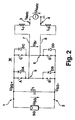
- a single-phase, transformerless inverter which according to the known embodiment in FIG. 2 two DC voltage terminals 1, 2, to which in this example an external solar generator SG is connected as a DC voltage source, and two AC voltage connections 3, 4 provides that are either connected to the conventional 50 Hz power grid or connected in the case of island operation to the electrical loads ,
- the single-phase, transformerless inverter W provides a buffer capacitor C 1 which is connected in parallel to a full bridge consisting of four switch units A, B, C, D and in each case with these anti-parallel connected, designated as freewheeling diodes rectifier diodes DA, DB, DC and DD.
- the individual switch units A, B, C, D are designed as high-frequency switches, which are suitable to realize switching operations with frequencies of up to several 100 kHz.
- Such switches are preferably designed as MOS field-effect transistors or as IGBT (Insulated Gate Bipolar Tansistor).
- a bridge tap takes place in each case in the middle of the parallel branches of the bridge circuit at the connection nodes 5, 6 between the respective switch units A, B and C, D by means of the connecting lines 7, 8.
- Both connecting lines 7, 8 are each via a reactor inductance L 1 and L 2 connected to the AC voltage terminals 3, 4. Between the connecting lines 7, 8 is the bridge voltage U Br at. Further, for safe operation of the in FIG. 2 components shown are not shown for reasons of clarity, such as. Filter to improve the electromagnetic compatibility (EMC) and parasitic elements, in particular capacities.
- EMC electromagnetic compatibility
- the switch units A, B, C, D In order to convert the solar generator voltage U SG into an alternating current required for mains supply or into an alternating voltage required in isolated operation, the switch units A, B, C, D must have a specific, high-frequency clock pattern which can have switching frequencies between a few kHz and a few 100 kHz to open in a coordinated manner and close to generate a time-discrete distinguishable voltage pulses whose potential location is matched to the externally applied in the islanding operation or alternating voltage generated U network. With the aid of the choke inductances L 1 , L 2 provided in the connecting lines 7, 8, it is possible to obtain a smooth, sinusoidal current or voltage curve at the outputs of the AC voltage terminals 3, 4.
- the diagonally opposite switch units ie A and D or B and C
- the control of the individual switch units takes place for a successful feed of electrical energy into the network such that during a positive half cycle of the AC voltage terminals 3, 4 AC voltage lying the switch units A, D according to a fixed clock pattern, eg. Based on a pulse width modulation ( PWM), high-frequency closed and opened, while the switch units B and C remain in the open state or are also driven in phase opposition to the switches A, D.
- PWM pulse width modulation
- the bridge voltage U Br takes in the case of closed switch units A and D or conductive free-wheeling diodes DA and DD the voltage + U SG , and in the case of the closed switch units B and C or conductive freewheeling diodes DB and DC the voltage -U SG .
- the reactor inductances L 1 and L 2 are ideally identical, the solar generator voltage U SG is divided symmetrically in all cases of symmetrical timing to the reference potential defined by the externally applied AC voltage (instantaneous value of the AC line voltage).
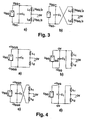
- FIGS. 3a and 3b Referenced In the case of FIG. 3a the switch units A and D are closed or DA and DD are conducting and an external reference potential of 0 V is assumed. Since the solar generator voltage is distributed symmetrically to the reference potential as shown above, the two connecting cables of the solar generator are at the potentials + U SG / 2 or -U SG / 2.
- FIG. 3b the case of the closed switch units B and C or conductive freewheeling diodes DB and DC is shown, which leads to the same potential ratios on the connection lines of the solar generator.
- the connecting cables of the solar generator are in accordance with FIG. 3a or FIG. 3b despite high-frequency clocking of the individual switch units A, B, C, D constant on the potentials + U SG / 2 and -U SG / 2.
- the switch positions A, B, C, D are each closed in pairs: A and D or B and C (as described above for the symmetrical case) or A and C or B and D are simultaneously closed and immediately alternate in a specific order, without allowing a circuit state in which all four switch units A, B, C, D are permanently open.
- This clocking has the following advantages: In the case of the additional switch configurations referred to as asymmetrical, in which A and C or B and D are closed at the same time, the bridge voltage U Br is reduced to 0 V.
- This circuit state also referred to as the "zero pointer" thus prevents this a commutation of the coil current via any freewheeling diodes to the buffer capacitor C 1 , whereby the efficiency of the inverter is decisively improved over the symmetric timing.
- the sum of instantaneous mains voltage and solar generator voltage U SG is not applied via the inductor inductances L 1 , L 2 , but only the instantaneous mains voltage U Netz , which contributes to the reduction of the coil current. Due to the much lower voltage, the current fluctuations (current ripple) in the output current are significantly smaller, which increases the efficiency and improves the electromagnetic compatibility.
- FIGS. 4a to 4d a disadvantage is inevitably associated with the unbalanced timing, based on the FIGS. 4a to 4d is shown. Only for the sake of easier understanding, it is assumed that the instantaneous AC voltage in the FIGS. 4a-d Removable equivalent circuits 0 V corresponds.
- the equivalent circuit diagrams according to the FIGS. 4a and 4c correspond to the circuit states with closed switch units A and D as well as B and C, thus according to the symmetrical clocking. In both cases, constant potentials are present at the connection lines of the solar generator SG, namely + U SG / 2 or - U SG / 2. In the in the Figures 4b and 4d shown circuit states, the switches A and C or B and D are closed.
- the connecting lines of the solar generator SG are no longer at the constant potentials + U SG / 2 or - U SG / 2, but they jump in the case of FIG. 4b to the values 0 V or - U SG and in the case of FIG. 4d on + U SG or 0 V.
- a third kind of clocking is the so-called single-phase chopping.
- a bridge branch e.g. B. the switches C, D, only with the mains frequency (50 Hz or 60 Hz) periodically switched, while the other bridge branch is clocked high-frequency sinusoidal modulation.
- the present invention seeks to provide an inverter, which combines the advantages of symmetrical and unbalanced clocking as well as the single-phase choping explained above and at the same time avoids the disadvantages associated with the above technique.
- an inverter is to be given while avoiding the use of complicated and costly circuit topologies, which has improved efficiency and better electromagnetic compatibility than previously known inverter.
- it is necessary to create a possibility for an optional grid or island operation of the inverter.
- an inverter with two DC voltage terminals, between which an intermediate energy storage device and a bridge circuit are provided in parallel circuit arrangement, which provides at least two parallel branches, each having two series-connected switch units, to each one Rectifier diode is connected in parallel, and with at least two AC voltage terminals, each of which is individually connected via a connecting line, in each of which a throttle inductance is connected to one of the parallel branches of the bridge circuit between two switch units via a connection node, further developed that between the at least two connection lines are provided two electrical connection paths, in each of which a switch and a rectifier diode connected in series are provided, and that the rectifier diodes are connected in the individual connection paths to each other in the opposite forward direction.
- the switches E and F are operated clocked during operation of the inverter.
- inventive concept also extends to possible equivalent embodiments of the circuit topology according to the invention, which can be obtained by using alternative electronic Bauelemenan extract and corresponding substitution of the combination of switch and rectifier diode in the connecting lines and the same or similar electrical or electronic Show effects in the switching behavior.
- a combination of switch and rectifier diode in training only a single electronic component is conceivable, its use is quite subsumed under the general concept of the invention.
- inverter which according to claim 1 provides two parallel connection paths between the two connecting lines.
- the measure according to the invention of providing the additional connection paths between the connection lines for tapping off the bridge voltage opens up the possibility for alternative freewheeling paths, along which the inductor current can propagate due to demagnetization processes of the inductor inductances.
- the efficiency of the inverter is significantly improved because no energy losses associated with the energy recovery in the buffer capacitor can occur.
- the sum of solar generator voltage and instantaneous mains voltage on the Drosselinduktstreeten but only the instantaneous mains voltage, which significantly reduces in the output current indicated in the prior art (symmetric timing) as shown disadvantageous current ripple can be.
- the additional freewheeling paths provided according to the invention during the freewheeling phase enable complete ohmic decoupling between the DC voltage connections and the DC voltage source connected thereto, preferably a solar generator, and the AC voltage connections.
- This has the consequence advantageously that high-frequency voltage jumps on the connecting lines of the solar generator, as they occur in the prior art (asymmetrical clocking or single-phase chopping), are avoided in principle.
- the hazard potential explained at the outset as well as the discussed problem with respect to the electromagnetic compatibility during operation of such an inverter is reduced to a degree of safety.
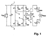
- inverter FIG. 1 a As the closest prior art described circuitry for an inverter, also has the invention designed according to inverter FIG. 1 a connected between the DC voltage terminals 1, 2 parallel circuit consisting of an intermediate energy storage C 1 , preferably in the form of a buffer capacitor, and a bridge circuit.
- the bridge circuit has the same as in FIG. 2 Bridge circuit shown four switch units A, B, C, D, to which respective rectifier diodes DA, DB, DC, DD are connected in parallel.
- the inventive difference to the known topology according to FIG. 2 consists in the provision of two additional electrical connection paths 9, 10 between the connecting lines 7, 8 for tapping the bridge voltage U Br to the connection node 5, 6.
- connection paths 9, 10 are each a switch E, F and a rectifier diode DE, DF , which are connected to each other in the opposite passage direction. All other circuit components correspond to those in FIG. 2 shown, known circuitry, so that no further reference must be made to the individual components.
- switch E and diode DE or switch F and diode DF in the individual connection paths 9, 10 is also to be replaced by the same effect component components that have the same Strom mallasseigenschaften in the individual connection paths 9, 10 as the switch E or F in combination with the diodes DE and DF respectively.
- the dashed diagonal connection 11 can optionally be inserted for this purpose, whereby the behavior of the circuit does not fundamentally change, but in practice the advantageous summary of the switch E and the diode DF or F and DE in one component, eg ., a parasitic diode MOSFET or in the form of an IGBT / diode co-pack.
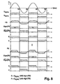
- the mode of operation of the inventively embodied inverter is carried out according to the symmetrical timing provided in the bridge circuit switch units A, B, C, D, ie, depending on the polarity of the half-waves of the mains voltage U net , the switch pairs A and D or B and C closed and opened according to a specified clock pattern.
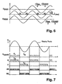
- the timing with which the individual switch units are switched AD is in the FIGS. 7 and 10 shown.
- FIG. 7 is the timing in the mode "grid feed" again, in which there is no reactive power demand, so at no time is a return of energy from the network in the buffer capacitor C 1 and in the DC voltage source U SG .
- the timing scheme shown enables complete so-called 4-quadrant operation, ie, the inverter serves as a voltage source for supplying energy to a load, the output of the inverter not being connected to a fixed AC voltage potential.
- This case corresponds to the island operation mentioned in the beginning.
- the choice of the two types of timing can be made depending on the application.
- time diagrams corresponds to the top diagram representation of the time course of the externally applied mains voltage U network .
- a suitable comparator circuit which is not discussed in detail, a rectangular synchronizing voltage U synch. are obtained, which at times of the positive half-wave of the mains voltage assumes a constant positive voltage value T P and at times of the negative half-wave, for example, 0 V.
- the switch units A, D and B, C in FIG. 7 driven.
- the switch units A, D synchronously closed at the beginning of the positive half-cycle in short successive clock pulses and open, in the middle of the time half of the positive half-wave, the periods extend in the closed state, until it towards the end of the positive half-wave in same as at the beginning only briefly closed.
- the switch units B, C are modulated, if the half-wave of the AC voltage is negative.
- PWM pulse width modulation
- the switching units A, B, C, D are applied with switching frequencies of up to several 100 kHz.
- the switches E, F are operated in the additional connection paths 9, 10 time synchronous with the AC frequency of the mains voltage U network , ie usually with 50 Hz.
- the switch E is closed during the majority of the positive half cycle while the switch F is open.
- the switch F closes during the majority of the negative half-wave when the switch position E.
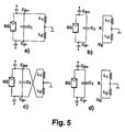
- FIGS. 5a and c provide equivalent circuit diagrams for the inverter topology in the cases of closed switch units A, D (see FIG. 5a ) and B, C (see FIG. 5c ). There is basically no difference to the known case (see FIG. 4a, c ).
- the freewheeling phases ie with open switch units A, D
- the in FIG. 5b illustrated state whereas the equivalent circuit diagram for the open switch position with respect to the switch units B, C of the FIG. 5d can be seen.
- FIG. 6 is a diagram showing that shows the voltages applied to the solar generator lines voltage curves. Symmetrical and time-synchronized, the positive and negative connection potential behave on the solar generator connection lines, with a maximum amplitude of U SG / 2 + in the case of the presence of an AC line voltage 2 ⁇ 230 / 2 V occurs at a frequency of 50 Hz.
- the rectifier diodes DA, DB, DC and DD serve as the prior art described above.
- the inductor current during the positive half cycle commutes with open switches A-F via the diodes DB and DC into the capacitor C 1 . Since the opening of the switches E and F takes place in time ranges in which the inductor currents have largely subsided, however, there are no appreciable current ripple effects which are capable of impairing the advantage of the circuit topology according to the invention.
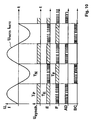
- a preferred embodiment of the timing of the switches E, F is based on the use of the error signal of the current controller and the phase information about the mains voltage.
- Such a present in the inverter control according to the prior art current controller always forms the difference between a sinusoidal current setpoint and the actual actual value of the current.
- the difference between the current setpoint value and the current actual value referred to as the error signal FS, is positive in the positive half-cycle, provided that the output current is lower than the setpoint value and negative, if it is above the setpoint value.
- This error signal FS has approximately a sinusoidal profile and controls the switch-on times of the switch units A to D via a pulse width modulator (PWM).
- PWM pulse width modulator
- the regulator reacts during the positive half cycle with a negative error signal, and vice versa during the negative half cycle (see in this regard FIG. 8 the small trained negative half-wave in the error signal FS towards the end of a positive half-wave or the formation of a small positive half-wave towards the end of the negative half-wave).
- This behavior in the error signal FS is advantageously used to control the switches E and F, in which the sign of the error signal SIGN (FS) with the synchronization signal U synch is logically connected via an AND operation.
- SIGN FS
- the feeding energy source can either be a solar generator (for example for emergency power supply with sufficient momentary solar generator power) or typically a battery storage or a fuel cell.
- the inverter itself must provide a voltage and frequency stable sinusoidal output voltage, for which he internally a sinusoidal voltage setpoint of z. As a table or generated by real-time calculation. Furthermore, it must also allow energy return from the grid towards the buffer capacitor or the feeding source (eg a battery) (4-quadrant operation). This is absolutely necessary in the case of island operation with reactive loads and corresponding phase shifts between current and voltage.
- the circuit is off FIG. 1 according to FIG. 9 extended by an output capacitor C 2 , which is connected via a switch S in the mode island operation in parallel with the output terminals of the inverter.
- This output capacitor C 2 acts in a known manner as an energy buffer in the output circuit and serves z.
- As the maintenance of the desired sinusoidal voltage at sudden load changes eg., For a load with phase control). Furthermore, a change in the timing of the switch according to FIG. 10 required in relation to grid-connected operation. While in the operating mode "mains supply” the inverter always works like a step-down converter and generates a sinus modulated lower output voltage from the high solar generator voltage, a temporary reversal of the energy flow direction is required in the mode "stand-alone operation", where the inverter works as a boost converter and energy from the low output voltage level to the higher voltage level of the input capacitor C 1 and the supplying battery high.
- the necessary behavior of the inverter as a boost converter can be controlled by a control of the switch FIG. 10 to reach.
- the switches E and F are clocked in push-pull to the bridge switches A, D and B, C in corresponding sections of the voltage setpoint here. So z. B. during the positive half cycle of the switch E as described permanently switched on, the switch F but in opposite phase to the switch pair A, D driven. This results in the possibility that a negative, in flowing into the inverter inductor current I establishes network with positive output voltage U mains through the closed switch F.
- the inductor current first commutates to the diodes DA and DD, so that an energy flow into the buffer capacitor C 1 or in the case of a supply of the inverter from a battery into this battery is possible. If after a small delay time, which is required to avoid overlaps of the closing times of the switches, the switches A and D are closed, the current can flow alternatively via these two elements back into the source.
- the freewheeling path 9 with the switch E and the diode DE is without function during this process of energy recovery, but immediately assumes its task as a freewheeling path for positive output currents I network in a reversal of the energy flow direction.
- the switch between the two modes can be done easily during operation, so that a 4-quadrant operation is also possible in grid parallel operation, if the inverter z. B. to be used for reactive current compensation or as an active harmonic filter. Furthermore, a switching between the types of clocking described in the prior art and the novel methods is possible to z. 8. Achieve a smooth transition from one halfwave to the other near the zero crossing.
Abstract
Description
Die Erfindung bezieht sich auf einen Wechselrichter zum Umformen einer elektrischen Gleichspannung in einen Wechselstrom oder eine Wechselspannung. Derartige Stromrichter werden bspw. zur elektrischen Energieeinspeisung in das öffentliche Stromnetz oder zur Bildung eines autarken Inselnetzes in Fällen eingesetzt, in denen lediglich Gleichspannungsenergiequellen zur Verfügung stehen, wie z. B. Photovoltaikanlagen, Brennstoffzellen, Batterien, etc..The invention relates to an inverter for converting a direct electrical voltage into an alternating current or an alternating voltage. Such converters are, for example, used for electrical energy supply in the public power grid or to form a self-sufficient island grid in cases where only DC power sources are available, such. As photovoltaic systems, fuel cells, batteries, etc ..
Bei einem Wechselrichter zur Einspeisung von Energie in ein vorhandenes Wechselspannungsnetz gilt es, einen Wechselstrom zu erzeugen, der in Bezug auf Phasenlage und Amplitude an den Potenzialverlauf der Wechselspannung, vorzugsweise einer 50 oder 60 Hz sinusförmig ausgebildeten Netzspannung, anzugleichen ist. Bei einem Wechselrichter zur Speisung eines autarken Inselnetzes hingegen gilt es, eine in Spannung und Frequenz stabile Wechselspannung zu erzeugen. Zum Betrieb beliebiger kapazitiver und induktiver Verbraucher muss ein solcher Wechselrichter in der Lage sein, Blindleistung abzugeben bzw. aufzunehmen.In the case of an inverter for feeding energy into an existing alternating voltage network, it is necessary to generate an alternating current which, in relation to the phase position and amplitude, is to be matched to the potential profile of the alternating voltage, preferably a 50 or 60 Hz sinusoidally formed mains voltage. In the case of an inverter for feeding a self-sufficient island grid, on the other hand, it is necessary to generate an AC voltage that is stable in voltage and frequency. For operation of any capacitive and inductive loads, such an inverter must be capable of delivering or receiving reactive power.
In an sich bekannter Weise dienen hierzu ein- oder dreiphasige Wechselrichter mit und ohne Transformator. Ein Überblick über die Vielzahl der dabei möglichen Ausführungsformen derartiger Wechselrichter findet sich in folgenden Quellennachweisen:
- [1]
Myrzik, Johanna, Topologische Untersuchungen zur Anwendung von tief/- hochsetzenden Stellern für Wechselrichter / Johanna Myrzik. - Kassel: kassel univ. press, 2001, Zugl.: Kassel, Univ., Diss. 2000, ISBN 3-933146-62-3 - [2]
Manfred Meyer, Leistungselektronik, Einführung, Grundlagen, Überblick, Springer-Verlag, Berlin Heidelberg New York London Paris Tokyo Hong Kong Barcelona 1990 - [3]
POWER ELECTRONICS, Converters, Applications and Design, Second Edition, JOHN WILEY & SONS, INC., New York Chichester Brisbane Toronto Singapore, 1989, 1995
- [1]
Myrzik, Johanna, Topological investigations on the application of low / high setting controllers for inverters / Johanna Myrzik. Kassel: Kassel univ. Press, 2001, Zugl .: Kassel, Univ., Diss. 2000, ISBN 3-933146-62-3 - [2]
Manfred Meyer, Power Electronics, Introduction, Basics, Overview, Springer-Verlag, Berlin Heidelberg New York London Paris Tokyo Hong Kong Barcelona 1990 - [3]
POWER ELECTRONICS, Converters, Applications and Design, Second Edition, JOHN WILEY & SONS, INC., New York Chichester Brisbane Toronto Singapore, 1989, 1995
Bei den genannten Anwendungsfällen stehen immer ein bei allen Belastungen hoher Umwandlungswirkungsgrad, ein gutes EMV-Verhalten, ein geringes Volumen und Gewicht sowie ein niedriger Preis im Vordergrund. Eine galvanische Trennung zwischen Gleich- und Wechselspannungsseite ist im Allgemeinen nicht erforderlich.For the applications mentioned above, high conversion efficiency, good EMC performance, low volume and weight as well as a low price are always in the foreground. Galvanic isolation between DC and AC side is generally not required.
Eine unter diesen Randbedingungen bislang günstigste Schaltung stellt eine transformatorlose Vollbrückenschaltung dar, die detailliert in [3] und [1] beschrieben ist. Hier werden ebenfalls die im weiteren näher erläuterten unterschiedlichen Taktungsarten der Vollbrückenschaltung dargestellt. Vorteilhaft bei dieser Topologie ist ein hoher Umwandlungswirkungsgrad und ein geringes Volumen und Gewicht. Nachteilig ist jedoch, abhängig von der eingesetzten Taktungsart, ein schlechtes EMV-Verhalten auf der Eingangsseite sowie teilweise das Fehlen eines 4-Quadranten-Betriebes (Blindleistungsfähigkeit).A circuit which has been the most favorable under these boundary conditions represents a transformerless full bridge circuit, which is described in detail in [3] and [1]. Here, the different types of timing of the full bridge circuit explained in more detail below are also shown. An advantage of this topology is a high conversion efficiency and a low volume and weight. However, a disadvantage is, depending on the used Taktungsart, a poor EMC behavior on the input side and partly the lack of a 4-quadrant operation (reactive power capability).
Ferner sind aus obigem Beitrag von Myrzik transformatorlose Wechselrichter-Topologien bekannt, die aus einer Kombination von tief- und hochsetzenden Stellern (Cuk- und Zeta-Wandlern) hervorgehen. Diese haben gegenüber den oben genannten Brückenschaltungen den Vorteil, dass die Eingangsspannung betragsmäßig sowohl kleiner als auch größer als der Maximalwert (Amplitude) der sinusförmigen Netzspannung sein kann. Bei der Brückenschaltung hingegen muss sie immer größer als die Netzspannungsamplitude sein, um eine Einspeisung in das Netz zu ermöglichen.Furthermore, from the above article by Myrzik transformerless inverter topologies are known, which emerge from a combination of low- and high-setting controllers (Cuk and Zeta converters). Compared to the bridge circuits mentioned above, these have the advantage that the input voltage is smaller in magnitude and larger than the maximum value (amplitude) of the sinusoidal mains voltage can be. In the bridge circuit, however, it must always be greater than the mains voltage amplitude in order to allow it to be fed into the grid.
Auf einem vergleichbaren Ansatz beruhen auch die in den
Bei allen zuletzt genannten Topologien ist jedoch als wesentlicher Nachteil zu nennen, dass entweder die gesamte oder zumindest ein großer Anteil der zum Ausgang übertragenen Energie in einer Drosselspule zwischengespeichert oder auch über Koppelkondensatoren zum Ausgang übertragen werden muss. Daraus resultiert bei allen Schaltungen ein gegenüber der einfachen Brückenschaltung deutlich geringerer Wirkungsgrad. Weiterhin sind sie z. T. sehr komplex und regelungstechnisch schwer beherrschbar.In all of the last-mentioned topologies, however, mention should be made of the significant disadvantage that either the entire or at least a large proportion of the energy transferred to the output has to be buffered in a choke coil or else has to be transmitted to the output via coupling capacitors. This results in all circuits compared to the simple bridge circuit significantly lower efficiency. Furthermore, they are z. T. very complex and control technology difficult to control.
Aus der
Die weiteren Ausführungen sollen im einzelnen das bestehende Wechselrichterproblem erhellen, insbesondere unter Bezugnahme auf einphasige, transformatorlose Wechselrichter, doch sei an dieser Stelle angemerkt, dass die im weiteren beschriebenen Maßnahmen grundsätzlich auch auf Wechselrichter jeweils mit Transformator übertragbar sind. Nur aus Gründen der Vollständigkeit sei ferner darauf hingewiesen, dass neben einphasigen Wechselrichtern auch mehrphasig arbeitende Geräte, vorzugsweise 3-phasige Wechselrichter, existieren, mit denen bspw. die Umwandlung von Gleichspannung in drei jeweils um 120° phasenverschobene periodische Strom- bzw. Spannungsverläufe möglich ist. Auch auf derartige, mehrphasige Wechselrichtersysteme können die im weiteren dargelegten Ausführungen Anwendung finden.The further explanations are intended to illuminate in detail the existing inverter problem, in particular with reference to single-phase, transformerless inverters, but it should be noted at this point that the measures described below are in principle also applicable to inverters each with transformer. Only for the sake of completeness is further pointed out that in addition to single-phase inverters and multiphase operating devices, preferably 3-phase inverters exist, with which, for example, the conversion of DC voltage into three phase-shifted by 120 ° periodic current or voltage waveforms is possible. The embodiments set forth below can also be applied to such multiphase inverter systems.
Betrachtet werde im weiteren die oben genannte und an sich bekannte Schaltungstopologie eines einphasigen, transformatorlosen Wechselrichters, der gemäß dem bekannten Ausführungsbeispiel in
Die einzelnen Schaltereinheiten A, B, C, D sind als Hochfrequenzschalter ausgebildet, die geeignet sind, Schaltvorgänge mit Frequenzen von bis zu einigen 100 kHz zu realisieren. Derartige Schalter sind vorzugsweise als MOS-FeldeffektTransistoren oder als IGBT (Insulated Gate Bipolar Tansistor) ausgebildet.The individual switch units A, B, C, D are designed as high-frequency switches, which are suitable to realize switching operations with frequencies of up to several 100 kHz. Such switches are preferably designed as MOS field-effect transistors or as IGBT (Insulated Gate Bipolar Tansistor).
Ein Brückenabgriff erfolgt jeweils mittig in den Parallelästen der Brückenschaltung an den Verbindungsknoten 5, 6 zwischen jeweils den Schaltereinheiten A, B sowie C, D mittels der Verbindungsleitungen 7, 8. Beide Verbindungsleitungen 7, 8 sind jeweils über eine Drosselinduktivität L1 bzw. L2 mit den Wechselspannungsanschlüssen 3, 4 verbunden. Zwischen den Verbindungsleitungen 7, 8 liegt die Brückenspannung UBr an. Weitere, für einen sicheren Betrieb der in
Zur Umwandlung der Solargeneratorspannung USG in einen zur Netzeinspeisung erforderlichen Wechselstrom oder in eine im Inselbetrieb erforderliche Wechselspannung gilt es, die Schaltereinheiten A, B, C, D mit einem bestimmten, hochfrequenten Taktmuster, das Schaltfrequenzen zwischen wenigen kHz bis zu einigen 100 kHz aufweisen kann, in aufeinander abgestimmter Weise zu öffnen und zu schließen, um zeitdiskret voneinander unterscheidbare Spannungspulse zu erzeugen, deren Potenziallage auf die extern angelegte bzw. im Inselbetrieb zu erzeugende Wechselspannung UNetz abgestimmt wird. Mit Hilfe der in den Verbindungsleitungen 7, 8 vorgesehenen Drosselinduktivitäten L1, L2 ist es möglich, an den Ausgängen der Wechselspannungsanschlüssen 3, 4 einen glatten, sinusförmigen Strom- bzw. Spannungsverlauf zu erhalten.In order to convert the solar generator voltage U SG into an alternating current required for mains supply or into an alternating voltage required in isolated operation, the switch units A, B, C, D must have a specific, high-frequency clock pattern which can have switching frequencies between a few kHz and a few 100 kHz to open in a coordinated manner and close to generate a time-discrete distinguishable voltage pulses whose potential location is matched to the externally applied in the islanding operation or alternating voltage generated U network. With the aid of the choke inductances L 1 , L 2 provided in the connecting
Grundsätzlich werden drei unterschiedliche Taktungsmuster, mit denen die Schaltereinheiten A, B, C, D innerhalb der konventionellen Brückenschaltung angesteuert werden, voneinander unterschieden.In principle, three different timing patterns with which the switch units A, B, C, D are driven within the conventional bridge circuit are distinguished from one another.
Im Falle der sog. symmetrischen Taktung werden stets die sich diagonal gegenüberliegenden Schaltereinheiten, d. h. A und D oder B und C zeitsynchron geschlossen bzw. geöffnet. Die Ansteuerung der einzelnen Schaltereinheiten erfolgt für eine erfolgreiche Einspeisung elektrischer Energie in das Netz derart, dass während einer positiven Halbwelle der an den Wechselspannungsanschlüssen 3, 4 anliegenden Netzwechselspannung die Schaltereinheiten A, D gemäß eines festgelegten Taktmusters, bspw. auf Basis einer Pulsweiten-Modulation (PWM), hochfrequent geschlossen und geöffnet werden, während die Schaltereinheiten B und C im geöffneten Zustand verharren oder auch gegenphasig zu den Schaltern A, D angesteuert werden. Während der Öffnungsphasen der Schalter A und D kommutiert der Strom durch die Drosselspulen L1, L2 auf die diagonal gegenüberliegenden Freilaufdioden DB und DC bzw. die geschlossenen Schalter B, C. Im umgekehrten Fall einer vom Netz vorgegebenen negativen Halbwelle, werden die Schaltereinheiten B und C nach dem entsprechenden Taktmuster geschlossen und geöffnet, während die Schaltereinheiten A und D in der geöffneten Stellung verbleiben oder auch gegenphasig zu den Schaltern B, C angesteuert werden. Jetzt kommutiert der Drosselstrom auf die Freilaufdioden DA und DD bzw. die geschlossenen Schalter A, D.
Dies vorausgesetzt führt zu folgenden elektrischen Eigenschaften des Wechselrichters: Die Brückenspannung UBr nimmt jeweils im Falle geschlossener Schaltereinheiten A und D bzw. leitender Freilaufdioden DA und DD die Spannung +USG an, und im Falle der geschlossenen Schaltereinheiten B und C bzw. leitender Freilaufdioden DB und DC die Spannung -USG. Setzt man ferner voraus, dass die Drosselinduktivitäten L1 und L2 ideal gleich ausgebildet sind, so teilt sich die Solargeneratorspannung USG in allen Fällen der symmetrischen Taktung symmetrisch zu dem durch die extern angelegte Wechselspannung definierten Bezugspotenzial (Momentanwert der Netz-Wechselspannung) auf.In the case of so-called symmetrical clocking, the diagonally opposite switch units, ie A and D or B and C, are always closed or opened in a time-synchronized manner. The control of the individual switch units takes place for a successful feed of electrical energy into the network such that during a positive half cycle of the
Provided this leads to the following electrical properties of the inverter: The bridge voltage U Br takes in the case of closed switch units A and D or conductive free-wheeling diodes DA and DD the voltage + U SG , and in the case of the closed switch units B and C or conductive freewheeling diodes DB and DC the voltage -U SG . Assuming further that the reactor inductances L 1 and L 2 are ideally identical, the solar generator voltage U SG is divided symmetrically in all cases of symmetrical timing to the reference potential defined by the externally applied AC voltage (instantaneous value of the AC line voltage).
Zur Verdeutlichung dieser Verhältnisse sei auf die
In
Berücksichtigt man weiterhin die an den Anschlussleitungen des Wechselrichters anliegende externe Wechselspannung, die sich ebenfalls aufgrund der Induktivitäten L1 und L2 symmetrisch auf beide Anschlussleitungen aufteilt, so führt dies an den Solargeneratoranschlüssen zu einer mit halber Netzamplitude UNetz/2 niederfrequent schwankenden Spannung, die keinerlei Sicherheitsprobleme sowie auch Probleme in Bezug auf die elektromagnetische Verträglichkeit aufwirft.Taking into account the voltage applied to the connection lines of the inverter external AC voltage, which is also divided symmetrically due to the inductors L 1 and L 2 on both leads, this leads to the solar generator terminals to a half network amplitude U net / 2 low-frequency fluctuating voltage, the There are no safety issues or electromagnetic compatibility issues.
Jedoch sind mit der symmetrischen Betriebsweise des Wechselrichters zwei Nachteile unvermeidbar verbunden. Betrachtet man bspw. während der positiven Halbwelle der Netzspannung jene Zeiträume, in denen die Schaltereinheiten A und D geöffnet sind und berücksichtigt man, dass der innerhalb der Drosselinduktivitäten L1 und L2 fließende Spulenstrom aufgrund von Entmagnetisierungsvorgängen innerhalb der Drosselinduktivitäten weiter aufrecht bleibt, so kommutiert dieser Spulenstrom während der sog. "Freilaufphase" über die Dioden DB und DC bzw. die geschlossenen Schalter B, C zurück in den Pufferkondensator C1, was mit erheblichen Verlusten verbunden ist, wodurch letztlich der Wirkungsgrad des Wechselrichters entscheidend negativ beeinflusst wird.However, two disadvantages are inevitably associated with the symmetrical operation of the inverter. If, for example, during the positive half-wave of the mains voltage, those periods in which the switch units A and D are opened are taken into account and it is taken into account that the coil current flowing within the inductance inductances L 1 and L 2 continues to be maintained due to demagnetization processes within the inductor inductances this coil current during the so-called "freewheeling phase" via the diodes DB and DC or the closed switch B, C back into the buffer capacitor C 1 , which is associated with significant losses, which ultimately decisively negatively affected the efficiency of the inverter.
Weiterhin entstehen beim periodischen Einschalten der Schalter A, D erhebliche Schaltverluste aufgrund der nicht idealen dynamischen Eigenschaften der Freilaufdioden DB und DC, entsprechend auch in der negativen Halbwelle.Furthermore, when the switches A, D are switched on periodically, considerable switching losses occur due to the non-ideal dynamic properties of the freewheeling diodes DB and DC, correspondingly also in the negative half-cycle.
Hinzu kommt, dass während der Kommutierung des Spulenstromes durch die Dioden DB und DC bzw. die geschlossenen Schalter B, C in den Kondensator C1 über den Drosselinduktivitäten L1 und L2 die Summe aus Eingangsspannung (z. B. die Solargeneratorspannung USG) und momentaner Netzspannung mit umgekehrter Polarität anliegt. Ein diesbezügliches Ersatzschaltbild ist der
Bei der sog. unsymmetrische Taktung treten im Gegensatz zur vorstehend erläuterten symmetrischen Taktung folgende, jeweils paarweise geschlossene Schalterstellungen der Schaltereinheiten A, B, C, D auf: A und D oder B und C (wie vorstehend zum symmetrischen Fall geschildert) oder A und C oder B und D sind gleichzeitig geschlossen und wechseln sich unmittelbar in bestimmter Reihenfolge ab, ohne dabei einen Schaltungszustand zuzulassen, in dem alle vier Schaltereinheiten A, B, C, D dauerhaft geöffnet sind.
Diese Taktung ist mit folgenden Vorteilen verbunden: Im Falle der als unsymmetrisch bezeichneten zusätzlichen Schalterkonstellationen, in denen A und C oder B und D gleichzeitig geschlossen sind, reduziert sich die Brückenspannung UBr auf 0 V. Dieser auch als "Nullzeiger" bezeichnete Schaltungszustand verhindert somit ein Kommutieren des Spulenstromes über etwaige Freilaufdioden hin zum Pufferkondensator C1, wodurch der Wirkungsgrad des Wechselrichters entscheidend gegenüber der symmetrischen Taktung verbessert wird. Weiterhin liegt im unsymmetrischen Schaltungszustand nicht die Summe aus momentaner Netzspannung und Solargeneratorspannung USG über den Drosselinduktivitäten L1, L2 an, sondern lediglich die momentane Netzspannung UNetz, die zum Abbau des Spulenstroms beiträgt. Aufgrund der sehr viel geringeren Spannung bilden sich die Stromschwankungen (Stromrippel) im Ausgangsstrom erheblich kleiner aus, wodurch der Wirkungsgrad steigt und auch die elektromagnetische Verträglichkeit verbessert wird.In the so-called unbalanced clocking, in contrast to the symmetrical clocking explained above, the switch positions A, B, C, D are each closed in pairs: A and D or B and C (as described above for the symmetrical case) or A and C or B and D are simultaneously closed and immediately alternate in a specific order, without allowing a circuit state in which all four switch units A, B, C, D are permanently open.
This clocking has the following advantages: In the case of the additional switch configurations referred to as asymmetrical, in which A and C or B and D are closed at the same time, the bridge voltage U Br is reduced to 0 V. This circuit state, also referred to as the "zero pointer", thus prevents this a commutation of the coil current via any freewheeling diodes to the buffer capacitor C 1 , whereby the efficiency of the inverter is decisively improved over the symmetric timing. Furthermore, in the unbalanced circuit state, the sum of instantaneous mains voltage and solar generator voltage U SG is not applied via the inductor inductances L 1 , L 2 , but only the instantaneous mains voltage U Netz , which contributes to the reduction of the coil current. Due to the much lower voltage, the current fluctuations (current ripple) in the output current are significantly smaller, which increases the efficiency and improves the electromagnetic compatibility.
Jedoch ist auch mit der unsymmetrischen Taktung ein Nachteil unvermeidbar verbunden, der anhand der
Bei einer von 0 V verschiedenen Netzspannung UNetz teilt sich diese in allen Taktphasen ebenfalls symmetrisch auf die beiden Drosselinduktivitäten L1 und L2 auf, so dass bspw. an der positiven Solargenerator-Anschlussleitung periodisch folgende Potenziale auftreten: (USG/2 + UNetz/2), (UNetz/2) sowie (USG + UNetz/2).In a different from 0 V mains voltage U network , this is also divided symmetrically in all clock phases on the two inductor inductances L 1 and L 2 , so that, for example, on the positive solar generator connecting line periodically following potentials occur: (U SG / 2 + U Network / 2), (U network / 2) and (U SG + U network / 2).
Eingedenk der Tatsache, dass typische Solargeneratorspannungen im Bereich zwischen 400 V und 750 V liegen, können unter Berücksichtigung des Potenzialbeitrages durch die Netzspannung an den Anschlußleitungen des Solargenerators Potenzialschwankungen zwischen 0 V und ca. 1 kV auftreten. Diese Potenzialschwankungen treten jedoch als hochfrequente Spannungssprünge mit Frequenzen von bis zu mehr als 100 kHz auf und führen zu überaus großen Ableitströmen über parasitäre Kapazitäten, wie sie an großflächigen Solargeneratoren typischerweise vorzufinden sind, wodurch die elektromagnetische Verträglichkeit derartiger Systeme entscheidend verschlechtert wird. Zudem stellen die hochfrequenten Spannungssprünge ein beträchtliches Gefährdungspotenzial bei Berührung der isolierten Moduloberflächen aufgrund einer kapazitiven Kopplung dar.Bearing in mind the fact that typical solar generator voltages lie in the range between 400 V and 750 V, potential fluctuations between 0 V and approx. 1 kV can occur, taking into account the potential contribution due to the grid voltage at the connection lines of the solar generator. However, these potential fluctuations occur as high-frequency voltage jumps with frequencies of up to more than 100 kHz and lead to extremely large leakage currents over parasitic capacitances, as typically found on large-area solar generators, whereby the electromagnetic compatibility of such systems is significantly deteriorated. In addition, the high-frequency voltage jumps represent a considerable potential hazard when touching the isolated module surfaces due to a capacitive coupling.
Eine dritte, in der vorstehenden Dissertation von Myrzik [1] beschriebene Taktungsart, stellt das sog. Einphasen-Chopping dar. Hierbei wird ein Brückenzweig, z. B. die Schalter C, D, nur mit der Netzfrequenz (50 Hz oder 60 Hz) periodisch umgeschaltet, während der andere Brückenzweig hochfrequent sinusmoduliert getaktet wird. So ist z. B. während der positiven Halbwelle der Schalter D permanent geschlossen, und die Schalter A, B werden getaktet. Hierdurch ergibt sich für den Zeitabschnitt, in dem sowohl der Schalter B als auch D gleichzeitig geschlossen sind, eine Brückenspannung von 0 V (Nullzeiger), so dass auch mit dieser Taktungsart wie bei der oben beschriebenen unsymmetrischen Taktung ein sehr guter Wirkungsgrad erzielt wird.A third kind of clocking, described in the above dissertation by Myrzik [1], is the so-called single-phase chopping. Here, a bridge branch, e.g. B. the switches C, D, only with the mains frequency (50 Hz or 60 Hz) periodically switched, while the other bridge branch is clocked high-frequency sinusoidal modulation. So z. B. during the positive half cycle of the switch D permanently closed, and the switches A, B are clocked. This results for the period in which both the switch B and D are closed at the same time, a bridge voltage of 0 V (zero pointer), so that even with this type of timing as In the above-described unbalanced clocking a very good efficiency is achieved.
Wie oben ergibt sich aber auch beim Einphasen-Chopping der gravierende Nachteil, dass abwechselnd entweder der positive oder der negative Pol des Solargenerators über die Schalter C, D mit dem Neutralleiter verbunden wird. Das Pozential des Solargenerators springt also periodisch um die Höhe der Solargeneratorspannung gegenüber Erdpotenzial, wodurch, wie oben dargestellt, erhebliche EMV-Probleme aufgeworfen werden.As above, however, there is also the serious disadvantage in single-phase chopping that alternately either the positive or the negative pole of the solar generator is connected via the switches C, D to the neutral conductor. The potential of the solar generator thus jumps periodically by the height of the solar generator voltage to earth potential, which, as shown above, considerable EMC problems are raised.
Ausgehend von dem vorstehend geschilderten Stand der Technik liegt der Erfindung die Aufgabe zugrunde, einen Wechselrichter anzugeben, der die Vorteile der vorstehend erläuterten symmetrischen und unsymmetrischen Taktung sowie des Einphasen-Choppings in sich vereint und gleichzeitig die mit der vorstehend genannten Technik verbundenen Nachteile vermeidet. Insbesondere soll ein Wechselrichter unter Vermeidung des Einsatzes komplizierter und kostenaufwändiger Schaltungstopologien angegeben werden, der über einen verbesserten Wirkungsgrad und eine bessere elektromagnetische Verträglichkeit als bisher bekannte Wechselrichter verfügt. Zudem gilt es, eine Möglichkeit für einen wahlweisen Netz- oder Inselbetrieb des Wechselrichters zu schaffen.Based on the above-described prior art, the present invention seeks to provide an inverter, which combines the advantages of symmetrical and unbalanced clocking as well as the single-phase choping explained above and at the same time avoids the disadvantages associated with the above technique. In particular, an inverter is to be given while avoiding the use of complicated and costly circuit topologies, which has improved efficiency and better electromagnetic compatibility than previously known inverter. In addition, it is necessary to create a possibility for an optional grid or island operation of the inverter.
Die Lösung der der Erfindung zugrunde liegenden Aufgabe ist im Anspruch 1 angegeben. Gegenstand der Ansprüche 10 und 20 betrifft eine alternative Ausgestaltung des erfindungsgemäßen Wechselrichters. Den Erfindungsgedanken vorteilhaft weiterbildende Merkmale sind Gegenstand der Unteransprüche sowie der Beschreibung unter Bezugnahme auf die Ausführungsbeispiele zu entnehmen.The solution of the problem underlying the invention is specified in claim 1. Subject matter of
Erfindungsgemäß ist ein Wechselrichter mit zwei Gleichspannungsanschlüssen, zwischen denen in paralleler Schaltungsanordnung ein Energiezwischenspeicher sowie eine Brückenschaltung vorgesehen sind, die wenigstens zwei Paralleläste, die jeweils zwei in Reihe geschaltete Schaltereinheiten vorsieht, zu denen jeweils eine Gleichrichterdiode parallel geschaltet ist, sowie mit wenigstens zwei Wechselspannungsanschlüssen, von denen jeder einzeln über eine Verbindungsleitung, in der jeweils eine Drosselinduktivität vorgesehen ist, mit einem der Paralleläste der Brückenschaltung jeweils zwischen zwei Schaltereinheiten über einen Verbindungsknoten verbunden ist, dadurch weitergebildet, dass zwischen den wenigstens zwei Verbindungsleitungen zwei elektrische Verbindungspfade vorgesehen sind, in denen jeweils ein Schalter sowie eine in Reihe geschaltete Gleichrichterdiode vorgesehen sind, und dass die Gleichrichterdioden in den einzelnen Verbindungspfaden zueinander in entgegengesetzter Durchlassrichtung geschaltet sind.
Wie im einzelnen aus den weiteren Ausführungen hervorgeht, werden die Schalter E und F während des Betriebes des Wechselrichter getaktet betrieben.According to the invention, an inverter with two DC voltage terminals, between which an intermediate energy storage device and a bridge circuit are provided in parallel circuit arrangement, which provides at least two parallel branches, each having two series-connected switch units, to each one Rectifier diode is connected in parallel, and with at least two AC voltage terminals, each of which is individually connected via a connecting line, in each of which a throttle inductance is connected to one of the parallel branches of the bridge circuit between two switch units via a connection node, further developed that between the at least two connection lines are provided two electrical connection paths, in each of which a switch and a rectifier diode connected in series are provided, and that the rectifier diodes are connected in the individual connection paths to each other in the opposite forward direction.
As can be seen in detail from the other comments, the switches E and F are operated clocked during operation of the inverter.
An dieser Stelle sei vermerkt, dass sich der Erfindungsgedanke zudem auch auf mögliche äquivalente Ausführungen zur erfindungsgemäßen Schaltungstopologie erstreckt, die durch Verwendung alternativer elektronischer Bauelemenanordnungen und entsprechende Substitution der Kombination aus Schalter und Gleichrichterdiode in den Verbindungsleitungen gewonnen werden können und gleiche oder ähnliche elektrische bzw. elektronische Wirkungen im Schaltverhalten zeigen. So ist insbesondere eine Kombination aus Schalter und Gleichrichterdiode in Ausbildung nur eines einzigen elektronischen Bauelementes denkbar, dessen Einsatz durchaus auch unter den allgemeinen Erfindungsgedanken zu subsummieren ist.At this point it should be noted that the inventive concept also extends to possible equivalent embodiments of the circuit topology according to the invention, which can be obtained by using alternative electronic Bauelemenanordnungen and corresponding substitution of the combination of switch and rectifier diode in the connecting lines and the same or similar electrical or electronic Show effects in the switching behavior. Thus, in particular, a combination of switch and rectifier diode in training only a single electronic component is conceivable, its use is quite subsumed under the general concept of the invention.
Zur einfacheren Darstellung des Erfindungsgedankens sei jedoch zunächst auf einen Wechselrichter Bezug genommen, der gemäß Anspruch 1 zwei parallel geführte Verbindungspfade zwischen den zwei Verbindungsleitungen vorsieht.To simplify the presentation of the inventive concept, however, reference is first made to an inverter, which according to claim 1 provides two parallel connection paths between the two connecting lines.
Mit der erfindungsgemäßen Maßnahme des Vorsehens der zusätzlichen Verbindungspfade zwischen den Verbindungsleitungen zum Abgriff der Brückenspannung eröffnet sich die Möglichkeit für alternative Freilaufpfade, längs der sich der Drosselstrom aufgrund Entmagnetisierungsvorgänge der Drosselinduktivitäten ausbreiten kann.The measure according to the invention of providing the additional connection paths between the connection lines for tapping off the bridge voltage opens up the possibility for alternative freewheeling paths, along which the inductor current can propagate due to demagnetization processes of the inductor inductances.
Hierdurch wird der Wirkungsgrad des Wechselrichters erheblich verbessert, da keine mit der Energierückspeisung in den Pufferkondensator verbundenen Energieverluste auftreten können. Zugleich liegt im Freilauffalle nicht wie beim Stand der Technik (symmetrische Taktung) die Summe aus Solargeneratorspannung und momentaner Netzspannung über den Drosselinduktivitäten an, sondern lediglich die momentane Netzspannung, wodurch die beim Stand der Technik (symmetrische Taktung) als nachteilhaft aufgezeigten Stromrippel im Ausgangsstrom deutlich reduziert werden können.As a result, the efficiency of the inverter is significantly improved because no energy losses associated with the energy recovery in the buffer capacitor can occur. At the same time is not the freewheeling trap as in the prior art (symmetric timing), the sum of solar generator voltage and instantaneous mains voltage on the Drosselinduktivitäten, but only the instantaneous mains voltage, which significantly reduces in the output current indicated in the prior art (symmetric timing) as shown disadvantageous current ripple can be.
Schließlich ermöglichen die zusätzlichen, erfindungsgemäß vorgesehenen Freilaufpfade während der Freilaufphase eine vollständige ohmsche Entkopplung zwischen den Gleichspannungsanschlüssen und der damit verbundenen Gleichspannungsquelle, vorzugsweise einem Solargenerator, und den Wechselspannungsanschlüssen. Dies hat in vorteilhafter Weise zur Folge, dass hochfrequente Spannungssprünge an den Anschlussleitungen des Solargenerators, wie sie beim Stand der Technik (unsymmetrische Taktung bzw. Einphasen-Chopping) auftreten, prinzipiell vermieden werden. Damit ist das eingangs erläuterte Gefährdungspotenzial sowie die diskutierte Problematik in Bezug auf die elektromagnetische Verträglichkeit beim Betrieb eines derartigen Wechselrichters zu einem Grad der Unbedenklichkeit reduziert.Finally, the additional freewheeling paths provided according to the invention during the freewheeling phase enable complete ohmic decoupling between the DC voltage connections and the DC voltage source connected thereto, preferably a solar generator, and the AC voltage connections. This has the consequence advantageously that high-frequency voltage jumps on the connecting lines of the solar generator, as they occur in the prior art (asymmetrical clocking or single-phase chopping), are avoided in principle. Thus, the hazard potential explained at the outset as well as the discussed problem with respect to the electromagnetic compatibility during operation of such an inverter is reduced to a degree of safety.
Weitere, mit dem erfindungsgemäßen ausgebildeten Wechselrichter verbundene Vorteile, die sich nicht zuletzt auf die Möglichkeit einer kostengünstigen Realisierung der hierfür erforderlichen Schaltungstopologie beziehen, werden im Weiteren unter Bezugnahme auf konkrete Ausführungsbeispiele näher erläutert.Further, associated with the inverter formed according to the invention advantages, which relate not least to the possibility of a cost-effective implementation of the circuit topology required for this purpose, will be explained in more detail below with reference to specific embodiments.
Die Erfindung wird nachstehend ohne Beschränkung des allgemeinen Erfindungsgedankens anhand von Ausführungsbeispielen unter Bezugnahme auf die Zeichnungen exemplarisch beschrieben. Es zeigen:
- Fig. 1
- schematisierter Schaltungsaufbau eines erfindungsgemäß ausgebildeten Wechselrichters,
- Fig. 2
- Wechselrichtertopologie gemäß Stand der Technik,
- Fig. 3
- Ersatzschaltbilder zur Erläuterung der symmetrischen Taktung beim bekannten Wechselrichter gem.
Figur 2 - Fig. 4
- Ersatzschaltbilder zur Erläuterung der unsymmetrischen Taktung beim bekannten Wechselrichter gem.
Figur 2 - Fig. 5
- Ersatzschaltbilder zur Erläuterung des Potenzialverhaltens beim erfindungsgemäß ausgebildeten Wechselrichter,
- Fig. 6
- Spannungsverlauf an der Anschlussleitung eines Solargenerators,
- Fig. 7
- Darstellung zum Taktverhalten einzelner Schaltereinheiten,
- Fig. 8
- Darstellung des Taktverhaltens einzelner Schaltereinheiten,
- Fig. 9
- Schematisierter Schaltungsaufbau eines erfindungsgemäß ausgebildeten Wechselrichters im Inselbetrieb sowie
- Fig. 10
- Darstellung zum Taktverhalten einzelner Schaltereinheiten im Inselbetrieb.
- Fig. 1
- schematic circuit structure of an inventively designed inverter,
- Fig. 2
- Inverter topology according to the prior art,
- Fig. 3
- Equivalent circuit diagrams for explaining the symmetric timing in the known inverter gem.
FIG. 2 . - Fig. 4
- Equivalent circuit diagrams for explaining the unbalanced clocking in the known inverter gem.
FIG. 2 . - Fig. 5
- Equivalent circuit diagrams for explaining the potential behavior in the inventively designed inverter,
- Fig. 6
- Voltage curve at the connection line of a solar generator,
- Fig. 7
- Representation of the clock behavior of individual switch units,
- Fig. 8
- Representation of the tact behavior of individual switch units,
- Fig. 9
- Schematized circuit structure of an inventively designed inverter in stand-alone operation as well
- Fig. 10
- Representation of the clock behavior of individual switch units in isolated operation.
Gleichsam dem unter Bezugnahme auf
Selbstverständlich ist die Bauelementkombination aus Schalter E und Diode DE bzw. Schalter F und Diode DF in den einzelnen Verbindungspfaden 9, 10 auch durch gleichwirkende Bauelementkomponenten zu ersetzen, die in den einzelnen Verbindungspfaden 9, 10 über die gleichen Stromdurchlasseigenschaften verfügen wie die Schalter E bzw. F in Kombination jeweils mit den Dioden DE bzw. DF. Zwischen den Verbindungspfaden kann hierzu auch optional die gestrichelt eingezeichnete diagonale Verbindung 11 eingefügt sein, wodurch sich das Verhalten der Schaltung nicht grundsätzlich ändert, aber in der Praxis die vorteilhafte Zusammenfassung des Schalters E und der Diode DF bzw. F und DE in einem Bauteil, bspw. eines MOS-Fet mit parasitärer Diode oder in Form eines IGBT/Diode-Co-Pack, ermöglicht.Of course, the combination of components of switch E and diode DE or switch F and diode DF in the
Die Betriebsweise des erfindungsgemäß ausgebildeten Wechselrichters erfolgt nach der eingangs erläuterten symmetrischen Taktung der in der Brückenschaltung vorgesehenen Schaltereinheiten A, B, C, D, d. h., in Abhängigkeit der Polarität der Halbwellen der Netzspannung UNetz werden die Schalterpaare A und D bzw. B und C nach einem festgelegten Taktmuster geschlossen und geöffnet. Das Zeitverhalten, mit dem die einzelnen Schaltereinheiten A-D geschaltet werden, ist in den
Das in
In dem in
Bspw. werden im Falle einer positiven Halbwelle die Schaltereinheiten A, D synchron zu Beginn der positiven Halbwelle in kurz aufeinander folgenden Taktpulsen geschlossen und geöffnet, im Bereich der zeitlichen Mitte der positiven Halbwelle verlängern sich die Zeitabschnitte im geschlossenen Zustand, bis sie gegen Ende der positiven Halbwelle in gleicher Weise wie zu Anfang nur kurzzeitig geschlossen werden. Mit dem gleichen Taktmuster werden die Schaltereinheiten B, C moduliert, sofern die Halbwelle der Wechselspannung negativ ist. Die Art und Weise einer derartigen Schalterbetätigung ist eine an sich unter dem Begriff Pulsweitenmodulation (PWM) bekannte Technik. Wie bereits einleitend erwähnt, werden die Schaltereinheiten A, B, C, D mit Schaltfrequenzen von bis zu einigen 100 kHz beaufschlagt.For example. be in the case of a positive half-wave, the switch units A, D synchronously closed at the beginning of the positive half-cycle in short successive clock pulses and open, in the middle of the time half of the positive half-wave, the periods extend in the closed state, until it towards the end of the positive half-wave in same as at the beginning only briefly closed. With the same clock pattern, the switch units B, C are modulated, if the half-wave of the AC voltage is negative. The manner of such a switch operation is a technique known per se by the term pulse width modulation (PWM). As mentioned in the introduction, The switching units A, B, C, D are applied with switching frequencies of up to several 100 kHz.
Im Gegensatz zu der hochfrequenten Taktweise, mit der die Schaltereinheiten A, B, C, D angesteuert werden, werden die Schalter E, F in den zusätzlichen Verbindungspfaden 9, 10 zeitsynchron mit der Wechselfrequenz der Netzspannung UNetz betrieben, d. h. üblicherweise mit 50 Hz. So wird im dargestellten Beispiel gemäß
Betrachtet man nun jene kurzzeitigen Momente, in denen bspw. der Schalter E geschlossen ist, also während der positiven Halbwelle der Netzspannung, und bei geöffneter Schalterstellung der Schalter A, D, so kommutiert der positive Spulenstrom auf die Diode DE und gelangt somit nicht zum Pufferkondensator C1 zurück. Ebenso ist im Falle der negativen Halbwelle der Schalter F geschlossen und bei geöffneter Schalterstellungen B, C kommutiert der Spulenstrom auf die Gleichrichterdiode DF (siehe hierzu
Es ergeben sich somit während des Betriebes des mit symmetrischer Taktung betriebenen Wechselrichters folgende in den
Somit liegt unter Voraussetzung idealer Bauelemente während der Freilaufphasen keine ohmsche Verbindung zwischen dem Solargenerator und dem Netz vor. Dies jedoch führt zu dem erfreulichen Vorteil, dass hochfrequente Spannungssprünge, wie sie beim eingangs beschrieben bekannten Wechselrichter mit unsymmetrischer Taktung oder Einphasen-Chopping auftreten, gänzlich vermieden werden können. Überdies bleibt während der Freilaufphasen das Potenzial der Anschlussleitungen des Solargenerators aufgrund bestehender parasitärer Kapazitäten Cp+ bzw. Cp- auf konstantem Potenzial. Diese Eigenschaft führt zu einer hohen elektromagnetischen Verträglichkeit ohne jegliches Gefährdungspotenzial.Thus, during operation of the inverter operated with symmetrical timing, the following result in the
Thus, assuming ideal components during the freewheeling phases there is no ohmic connection between the solar generator and the grid. However, this leads to the pleasing advantage that high-frequency voltage jumps, as they occur in the inverter known in the introduction with asymmetrical timing or single-phase chopping, can be completely avoided. Moreover, during the freewheeling phases, the potential of the connecting lines of the solar generator remains at a constant potential due to existing parasitic capacitances C p + and C p- . This property leads to a high electromagnetic compatibility without any danger potential.
Selbst wenn die eingesetzten Drosselspulen L1 und L2 nicht exakt über identische Induktivitäten verfügen - eine Forderung, die bei einer Schaltung nach dem Stand der Technik und symmetrischer Taktung mit großem Bedacht einzuhalten ist, will man den hochfrequenten Potenzialsprüngen Einhalt gebieten -, verschieben sich bei der erfindungsgemäßen Schaltung die mittleren Potenziale während beider Halbwellen nur geringfügig gegeneinander, sie sind nicht mehr exakt +/- Usg/2. Damit tritt beim Wechsel von einer Halbwelle zur anderen, d. h. mit 50 Hz, ein kleiner Potenzialsprung auf, der aber leicht beherrschbar ist. Somit können die Drosselinduktivitäten durchaus übliche Toleranzen aufweisen, gleichwohl die EMV erheblich verbessert ist.Even if the inductors used L1 and L2 do not have exactly the same inductances - a requirement that must be observed with great care in a circuit according to the prior art and symmetrical timing, you want to stop the high-frequency potential jumps - move in the inventive Switching the mean potentials during both half waves only slightly against each other, they are no longer exactly +/- Usg / 2. This occurs when changing from one half-wave to the other, d. H. with 50 Hz, a small potential jump on, but which is easy to control. Thus, the reactor inductances may well have usual tolerances, however, the EMC is significantly improved.
Aus ![]()
![]()
Ein weiterer interessanter Aspekt betrifft die Ausbildung der Gleichrichterdioden DA, DB, DC sowie DD, für deren Diodenqualität im Falle des erfindungsgemäß ausgebildeten Wechselrichters keine besonderen Anforderungen bestehen, da sie in den Freilaufphasen keine erwähnenswerte Kommutierungsfunktionen übernehmen, da die Kommutierung des Drosselstromes während der Freilaufphasen je nach Polarität der Halbwelle der Netzspannung über die Gleichrichterdioden DE bzw. DF erfolgt. Gleichwohl ihre Bedeutung und somit der Qualitätsanspruch an die Gleichrichterdioden reduziert ist, kann auf sie nicht völlig verzichtet werden. Der Grund hierfür liegt in der Notwendigkeit einer möglichst vollständigen Entmagnetisierung der Drosselinduktivitäten L1, L2 gegen Ende einer jeden Netzhalbwelle, die bei geschlossener Stellung des Schalters E bzw. F aufgrund der niedrigen zum Stromabbau zur Verfügung stehenden Netzspannung nicht gewährleistet werden kann. Aus diesem Grund sind die Schalter E bzw. F nicht während der gesamten Dauer der jeweiligen Halbwelle geschlossen, sondern öffnen bereits kurz vor Ende der jeweiligen Halbwellen, wie dies im Übrigen auch aus der Gegenüberstellung des Zeitverhaltens der einzelnen Schalter in Bezug auf die Halbwelle gemäß
Das zeitliche Ansteuern der Schaltereinheiten E und F erfolgt über eine Steuereinheit, die im einfachsten Ausführungsbeispiel über diskrete Zeitglieder realisierbar ist. Nachteilhaft bei der Verwendung von Zeitgliedern mit konstanter Einschaltzeit TE bzw. TF ist die Tatsache, dass nicht ausgeschlossen werden kann, dass die Schalter E, F in Bezug auf den Verlauf der Wechselspannung zu früh oder zu spät geöffnet werden, wodurch Wirkungsgradverluste sowie EMV-Probleme, wie sie aus dem Stand der Technik bekannt sind, auftreten.The timing of the switch units E and F via a control unit, which in the simplest embodiment on discrete timers is feasible. What is disadvantageous about the use of timers with a constant on-time T E or T F is the fact that it can not be ruled out that the switches E, F are opened too early or too late with respect to the course of the AC voltage, as a result of which efficiency losses and EMC Problems, as they are known from the prior art occur.
Eine bevorzugte Ausführung des zeitlichen Ansteuerns der Schalter E, F basiert auf der Nutzung des Fehlersignals des Stromreglers und der Phaseninformation über die Netzspannung. Ein derartiger gemäß dem Stand der Technik in der Wechselrichtersteuerung vorhandener Stromregler bildet stets die Differenz aus einem sinusförmigen Strom-Sollwert und dem tatsächlichen Strom-Istwert.
Die als Fehlersignal FS bezeichnete Differenz aus Strom-Sollwert und Strom-Istwert ist in der positiven Halbwelle positiv, sofern der Ausgangsstrom kleiner als der Sollwert ist und negativ, falls er über dem Sollwert liegt. Dieses Fehlersignal FS verfügt näherungsweise über einen sinusförmigen Verlauf und steuert über einen Pulsweiten-Modulator (PWM) die Einschaltzeiten der Schaltereinheiten A bis D.A preferred embodiment of the timing of the switches E, F is based on the use of the error signal of the current controller and the phase information about the mains voltage. Such a present in the inverter control according to the prior art current controller always forms the difference between a sinusoidal current setpoint and the actual actual value of the current.
The difference between the current setpoint value and the current actual value, referred to as the error signal FS, is positive in the positive half-cycle, provided that the output current is lower than the setpoint value and negative, if it is above the setpoint value. This error signal FS has approximately a sinusoidal profile and controls the switch-on times of the switch units A to D via a pulse width modulator (PWM).
Im oben beschriebenen Fall eines zu langsam abklingenden Drosselstromes reagiert der Regler während der positiven Halbwelle mit einem negativen Fehlersignal, und entsprechend umgekehrt während der negativen Halbwelle (siehe hierzu in
Mit Hilfe einer derartigen, selbstregelnden Zeittaktung der Schalter E sowie F können deren Öffnungszeitpunkte automatisch optimal bestimmt werden. Auf diese Weise kann der höchste Wirkungsgrad bei geringsten Verzerrungen im Strom und geringsten EMV-Probleme beim Betrieb des erfindungsgemäßen Wechselrichters erzielt werden.With the help of such, self-regulating time clocking of the switches E and F their opening times can be automatically determined optimally. In this way For example, the highest efficiency with the lowest distortion in the current and the lowest EMC problems during operation of the inverter according to the invention can be achieved.
Eine alternative, technisch durchaus realisierbare Ausführungsform eines erfindungsgemäß ausgebildeten Wechselrichters ist ebenso denkbar, indem anstelle der vorstehend beschriebenen Verbindungspfade 9, 10 mit den darin enthaltenen Schaltern E, F sowie Gleichrichtern DE, DF ein einziger Verbindungspfad mit einem einzigen, hochfrequent schaltenden Schalter eingesetzt wird. Der einzige hochfrequent schaltende Schalter ist gerade zu jenen Zeiten zu schließen, in denen die Schaltereinheiten A bis D, wie sie vorstehend erläutert mit einer symmetrischen Taktung betrieben werden, geöffnet sind. Ebenso gilt es, den Schalter gegen Ende der Halbwellen in der entsprechenden geöffneten Stellung zu belassen, um den Entmagnetisierungsvorgang der Drosselinduktivitäten L1, L2, wie vorstehend erläutert, abklingen zu lassen.An alternative, technically quite feasible embodiment of an inventively designed inverter is also conceivable by instead of the above-described
Die in
Für einen Inselbetrieb wird daher die Schaltung aus
For island operation, therefore, the circuit is off
Dieser Ausgangskondensator C2 wirkt in bekannter Weise als Energiepuffer im Ausgangskreis und dient z. B. der Aufrechterhaltung der gewünschten sinusförmigen Spannung bei sprunghaften Laständerungen (z. B. bei einer Last mit Phasenanschnittsteuerung).
Weiterhin ist eine Änderung der Taktung der Schalter gemäß
Furthermore, a change in the timing of the switch according to
Die Umschaltung zwischen den beiden Betriebsarten kann problemlos im laufenden Betrieb erfolgen, so dass ein 4-Quadranten-Betrieb auch im Netzparallelbetrieb möglich ist, falls der Wechselrichter z. B. zur Blindstromkompensation oder als aktives Oberwellenfilter eingesetzt werden soll. Weiterhin ist auch eine Umschaltung zwischen den im Stand der Technik beschriebenen Taktungsarten und den neuartigen Verfahren möglich, um z. 8. in der Nähe des Nulldurchganges einen glatten Übergang von einer Halbwelle zur anderen zu erzielen.The switch between the two modes can be done easily during operation, so that a 4-quadrant operation is also possible in grid parallel operation, if the inverter z. B. to be used for reactive current compensation or as an active harmonic filter. Furthermore, a switching between the types of clocking described in the prior art and the novel methods is possible to z. 8. Achieve a smooth transition from one halfwave to the other near the zero crossing.
- 1, 21, 2
- GleichspannungsanschlüsseDC terminals
- 3, 43, 4
- WechselspannungsanschlüsseAC terminals
- 5, 65, 6
- Verbindungsknotenconnecting node
- 7, 87, 8
- Verbindungsleitungeninterconnectors
- 9, 109, 10
- Verbindungspfadeconnection paths
- 1111
- Elektrische VerbindungElectrical connection
- 1212
- Verbindungspfadconnection path
- SGSG
- Solargeneratorsolar generator
- C1 C 1
- Pufferkondensator (Eingang)Buffer capacitor (input)
- C2 C 2
- Pufferkondensator (Ausgang)Buffer capacitor (output)
- A, B, C, DA, B, C, D
- Schaltereinheitenswitch units
- E, F, SE, F, S
- Schalterswitch
- DA, DB, DC, DD, DE, DFDA, DB, DC, DD, DE, DF
- GleichrichterdiodenRectifier diodes
- L1, L2 L 1 , L 2
- Drosselinduktivitäteninductors
- WW
- Wechselrichterinverter
- SGSG
- Solargeneratorsolar generator
- KK
- Knotenpunktjunction
Claims (11)
dadurch gekennzeichnet, dass
characterized in that
ein Paar von Schaltereinheiten (A, D; B, C) der Brückenschaltung während einer Mehrzahl von Zeitabschnitten geöffnet sind, und
die Schaltungsanordnung zumindest in einem Teil der Mehrzahl von Zeitabschnitten in dem ersten Zustand ist.An inverter according to claim 1, which is operable such that
a pair of switch units (A, D; B, C) of the bridge circuit are opened during a plurality of periods, and
the circuitry is at least part of the plurality of time periods in the first state.
ein erstes Paar von Schaltereinheiten aus der Schaltereinheit (A) aufgebaut ist, die betreibbar ist, um eine Verbindung zwischen dem ersten Anschluss des Energiezwischenspeichers (C1) und der ersten Drosselinduktivität (L1) zu ermöglichen, sowie der Schaltereinheit (D), die betreibbar ist, um eine Verbindung zwischen dem zweiten Anschluss des Energiezwischenspeichers (C1) und der zweiten Drosselinduktivität (L2) zu ermöglichen,
ein zweites Paar von Schaltereinheiten aus der Schaltereinheit (B) aufgebaut ist, die betreibbar ist, um eine Verbindung zwischen dem zweiten Anschluss des Energiezwischenspeichers (C1) und der ersten Drosselinduktivität (L1) zu ermöglichen, sowie der Schaltereinheit (C), die betreibbar ist, um eine Verbindung zwischen dem ersten Anschluss des Energiezwischenspeichers (C1) und der zweiten Drosselinduktivität (L2) zu ermöglichen.An inverter according to claim 2, wherein
a first pair of switch units is constructed from the switch unit (A) operable to enable a connection between the first terminal of the energy accumulator (C1) and the first inductance inductor (L1) and the switch unit (D) which is operable in order to enable a connection between the second terminal of the energy buffer (C1) and the second reactor inductance (L2),
a second pair of switch units is constructed from the switch unit (B) operable to enable connection between the second terminal of the energy accumulator (C1) and the first inductance inductor (L1) and the switch unit (C) which is operable to allow a connection between the first terminal of the intermediate energy storage device (C1) and the second Drosselinduktivität (L2).
gekennzeichnet durch
marked by
Applications Claiming Priority (2)
| Application Number | Priority Date | Filing Date | Title |
|---|---|---|---|
| DE10221592A DE10221592A1 (en) | 2002-05-15 | 2002-05-15 | Current inverter for direct/alternating currents, has direct and alternating connections with an intermediate power store, a bridge circuit, rectifier diodes and a inductive choke |
| EP03009882A EP1369985B1 (en) | 2002-05-15 | 2003-05-15 | Inverter for transforming a DC voltage into an AC current or an AC voltage |
Related Parent Applications (2)
| Application Number | Title | Priority Date | Filing Date |
|---|---|---|---|
| EP03009882.6 Division | 2003-05-15 | ||
| EP03009882A Division EP1369985B1 (en) | 2002-05-15 | 2003-05-15 | Inverter for transforming a DC voltage into an AC current or an AC voltage |
Publications (3)
| Publication Number | Publication Date |
|---|---|
| EP2086102A2 true EP2086102A2 (en) | 2009-08-05 |
| EP2086102A3 EP2086102A3 (en) | 2009-12-02 |
| EP2086102B1 EP2086102B1 (en) | 2010-09-22 |
Family
ID=29413842
Family Applications (2)
| Application Number | Title | Priority Date | Filing Date |
|---|---|---|---|
| EP09006359A Expired - Lifetime EP2086102B1 (en) | 2002-05-15 | 2003-05-15 | Inverter for converting an electric direct current into an alternating current or an alternating voltage |
| EP03009882A Expired - Lifetime EP1369985B1 (en) | 2002-05-15 | 2003-05-15 | Inverter for transforming a DC voltage into an AC current or an AC voltage |
Family Applications After (1)
| Application Number | Title | Priority Date | Filing Date |
|---|---|---|---|
| EP03009882A Expired - Lifetime EP1369985B1 (en) | 2002-05-15 | 2003-05-15 | Inverter for transforming a DC voltage into an AC current or an AC voltage |
Country Status (6)
| Country | Link |
|---|---|
| EP (2) | EP2086102B1 (en) |
| AT (2) | ATE431640T1 (en) |
| DE (3) | DE10221592A1 (en) |
| DK (1) | DK2086102T3 (en) |
| ES (2) | ES2352448T3 (en) |
| PT (1) | PT2086102E (en) |
Cited By (3)
| Publication number | Priority date | Publication date | Assignee | Title |
|---|---|---|---|---|
| CN102263520A (en) * | 2011-07-08 | 2011-11-30 | 阳光电源股份有限公司 | Circuit, method and convertor for converting direct voltage into alternating voltage |
| US20130016550A1 (en) * | 2011-07-13 | 2013-01-17 | Delta Electronics, Inc. | Inverter |
| CN103904930A (en) * | 2014-04-01 | 2014-07-02 | 燕山大学 | Three-phase seven-switch photovoltaic grid-connected inverter |
Families Citing this family (75)
| Publication number | Priority date | Publication date | Assignee | Title |
|---|---|---|---|---|
| AT413914B (en) * | 2004-02-12 | 2006-07-15 | Felix Dipl Ing Dr Himmelstoss | Conversion circuit changing input voltage into two symmetrical unipolar voltages |
| DE102004030912B3 (en) | 2004-06-25 | 2006-01-19 | Sma Technologie Ag | Method for converting a direct electrical voltage of a DC voltage source, in particular a photovoltaic DC voltage source into an AC voltage |
| DE102005024465B4 (en) * | 2005-05-24 | 2010-01-07 | Hantschel, Jochen, Dipl.-Ing. (FH) | Circuit arrangement and control method for a converter |
| DE102005047373A1 (en) * | 2005-09-28 | 2007-04-05 | Schekulin, Dirk, Dr. Ing. | Low-setting plate circuit consists of input and output connections with main branches between them as well as input-side condenser and output-side diode series connections |
| DE102006012164B4 (en) * | 2005-12-23 | 2009-12-17 | Fraunhofer-Gesellschaft zur Förderung der angewandten Forschung e.V. | Circuit arrangement for generating an alternating voltage or an alternating current |
| DE102006010694B4 (en) * | 2006-03-08 | 2010-01-07 | Refu Elektronik Gmbh | Inverter circuit for extended input voltage range |
| ES2541772T3 (en) | 2006-07-31 | 2015-07-24 | Ingeteam Power Technology, S.A. | Single phase inverter circuit for conditioning and converting direct current electrical energy into alternating current electrical energy |
| DE102007026393B4 (en) | 2007-06-06 | 2009-03-12 | Refu Elektronik Gmbh | Circuit arrangement and control method for an inverter with boost converter |
| DE102007028078B4 (en) | 2007-06-15 | 2009-04-16 | Sma Solar Technology Ag | Device for feeding electrical energy into a power supply network and DC-DC converter for such a device |
| DE102007028077B4 (en) | 2007-06-15 | 2009-04-16 | Sma Solar Technology Ag | Device for feeding electrical energy into a power supply network and DC-DC converter for such a device |
| DE102007029767B3 (en) * | 2007-06-22 | 2008-12-24 | Fraunhofer-Gesellschaft zur Förderung der angewandten Forschung e.V. | inverter |
| DE102007030577A1 (en) | 2007-06-29 | 2009-01-02 | Sma Solar Technology Ag | Inverter for feeding electrical energy into a power supply network |
| EP2023475B1 (en) * | 2007-08-04 | 2016-10-12 | SMA Solar Technology AG | Inversion for a grounded DC source, in particular a photovoltaic generator |
| DE102007038959A1 (en) | 2007-08-14 | 2009-02-26 | Sma Solar Technology Ag | inverter |
| DE102007038960A1 (en) | 2007-08-14 | 2009-02-26 | Sma Solar Technology Ag | inverter |
| ATE452460T1 (en) | 2007-10-19 | 2010-01-15 | Sma Solar Technology Ag | INVERTERS, ESPECIALLY FOR PHOTOVOLTAIC SYSTEMS |
| EP2051364A3 (en) | 2007-10-19 | 2016-08-10 | Diehl AKO Stiftung & Co. KG | Method for operating an inverter |
| DE102007058633B4 (en) | 2007-10-19 | 2009-12-24 | Diehl Ako Stiftung & Co. Kg | Method for operating an inverter |
| WO2009152600A1 (en) | 2008-06-16 | 2009-12-23 | Xantrex International | Method and apparatus for converting direct current into an alternating current |
| AU2008357911B2 (en) | 2008-06-17 | 2013-10-17 | Ingeteam Power Technology, S.A. | Control method for a structure converting direct current into alternating current |
| EP2136465B1 (en) | 2008-06-18 | 2017-08-09 | SMA Solar Technology AG | Inverter realized by a bridge circuit comprising slow and fast clocked switches |
| EP2144359A2 (en) | 2008-07-09 | 2010-01-13 | SMA Solar Technology AG | DC/DC-converter |
| ATE545190T1 (en) | 2008-07-09 | 2012-02-15 | Sma Solar Technology Ag | DC/DC CONVERTER |
| DE102008048841B8 (en) | 2008-09-25 | 2010-06-10 | Fraunhofer-Gesellschaft zur Förderung der angewandten Forschung e.V. | Isolating circuit for inverter |
| DE112009004376A5 (en) * | 2008-12-20 | 2013-03-28 | Sma Solar Technology Ag | TRANSFORMERLESS INVERTER WITH A DC / DC CONVERTER |
| DE102008063201A1 (en) | 2008-12-29 | 2010-07-22 | Martin Weinmann | Method and circuit arrangement for feeding the voltage intermediate circuit of an inverter |
| EP2226926A1 (en) | 2009-03-02 | 2010-09-08 | ABB Research Ltd. | Five-level inverter |
| EP2237403A1 (en) * | 2009-03-30 | 2010-10-06 | SMA Solar Technology AG | Inverter with two asymmetric bridges and a free-wheeling path decoupling the DC input from the AC output |
| EP2309639B1 (en) * | 2009-10-09 | 2016-02-10 | SMA Solar Technology AG | Reactive power-capable inverter |
| DE102010016138A1 (en) | 2010-03-25 | 2011-09-29 | Refu Elektronik Gmbh | Solar inverter for extended irradiation value range and operating method |
| EP2577859A2 (en) | 2010-06-07 | 2013-04-10 | ABB Inc. | Inverter for solar cell array |
| JP5658368B2 (en) * | 2010-08-17 | 2015-01-21 | パイル セウPAIL Ceu | Improved circuit device for transformerless single-phase PV inverter |
| CN102611347A (en) * | 2011-01-21 | 2012-07-25 | 北京动力源科技股份有限公司 | Single-phase non-isolated solar grid-connected inverter |
| CN102624274A (en) * | 2011-01-30 | 2012-08-01 | 上海康威特吉能源技术有限公司 | Interleaving parallel grid-connected inverter and control method thereof |
| CN102163935A (en) * | 2011-03-04 | 2011-08-24 | 东南大学 | Photovoltaic grid-connected converter with alternating bypass unit |
| CN102684218B (en) * | 2011-03-16 | 2014-07-16 | 南京航空航天大学 | Non-isolating photovoltaic grid-connected inverter |
| CN102158110A (en) * | 2011-04-07 | 2011-08-17 | 江苏斯达工业科技有限公司 | Main circuit of non-isolated photovoltaic grid inverter and control realizing method thereof |
| US11901810B2 (en) | 2011-05-08 | 2024-02-13 | Koolbridge Solar, Inc. | Adaptive electrical power distribution panel |
| US8937822B2 (en) | 2011-05-08 | 2015-01-20 | Paul Wilkinson Dent | Solar energy conversion and utilization system |
| CN102185511B (en) * | 2011-05-09 | 2013-04-24 | 浙江金贝能源科技有限公司 | Noninsulated type converting circuit from direct-current voltage to alternating-current voltage |
| JP6155532B2 (en) * | 2011-05-31 | 2017-07-05 | パナソニックIpマネジメント株式会社 | Power supply system |
| DE102011051954B4 (en) * | 2011-07-19 | 2013-08-14 | Refusol Gmbh | Photovoltaic system with bias on the inverter |
| DE102011081111A1 (en) * | 2011-08-17 | 2013-02-21 | Siemens Aktiengesellschaft | Inverter assembly |
| CN103036463A (en) * | 2011-10-10 | 2013-04-10 | 艾伏新能源科技(上海)股份有限公司 | High efficiency single-phase photovoltaic grid-connected inverter |
| DE102011115728B4 (en) * | 2011-10-12 | 2022-11-17 | Sew-Eurodrive Gmbh & Co Kg | Method of operating an inverter and inverter circuit |
| CN102361408A (en) * | 2011-10-20 | 2012-02-22 | 东南大学 | Non-isolated photovoltaic grid-connected inverter and switching control time sequence thereof |
| DE102011116593B4 (en) | 2011-10-21 | 2014-11-13 | Diehl Ako Stiftung & Co. Kg | Inverter with asymmetrical chokes and a control unit for asymmetric operation of the chokes |
| EP2595305A1 (en) | 2011-11-21 | 2013-05-22 | Vincotech GmbH | Assymetric twin bridge DC/AC inverter capable of reactive power transfer |
| US8867248B2 (en) | 2011-12-20 | 2014-10-21 | Kohler Co. | High-efficiency, three-level, single-phase inverter |
| WO2014004575A1 (en) | 2012-06-25 | 2014-01-03 | Arizona Board Of Regents, For And On Behalf Of Arizona State University | Circuits and methods for photovoltaic inverters |
| CN102790399B (en) * | 2012-07-25 | 2015-09-09 | 华为技术有限公司 | Power grid reactive compensation method, device and combining inverter |
| CN103580524A (en) * | 2012-08-07 | 2014-02-12 | 郭晓瑞 | Novel H4 bridge multi-level grid-connected-connected inverter circuit |
| CN102916445B (en) * | 2012-10-24 | 2014-12-10 | 西安理工大学 | Single-phase grid-connected photovoltaic power generating device capable of inhibiting common mode current |
| CN103269174B (en) * | 2012-12-10 | 2016-12-21 | 国网江西省电力公司南昌供电分公司 | A kind of single-phase photovoltaic grid-connected inverter of low common-mode voltage |
| CN103051233B (en) * | 2012-12-12 | 2015-02-18 | 东南大学 | Non-isolated single-phase photovoltaic grid-connected inverter and on-off control timing sequence thereof |
| EP2980980B1 (en) * | 2013-03-28 | 2021-05-26 | Panasonic Intellectual Property Management Co., Ltd. | Inverter device |
| TWI488421B (en) * | 2013-04-03 | 2015-06-11 | Delta Electronics Inc | Dc-to-ac power conversion system and method of operating the same |
| CN103178739B (en) * | 2013-04-17 | 2014-12-10 | 东南大学 | Zero-voltage transition full-bridge non-isolated photovoltaic grid-connected inverter |
| DE102013211121A1 (en) | 2013-06-14 | 2014-12-18 | Robert Bosch Gmbh | inverter |
| JP6136011B2 (en) * | 2013-08-02 | 2017-05-31 | パナソニックIpマネジメント株式会社 | Semiconductor device and power conversion device |
| CN103684030A (en) * | 2013-12-30 | 2014-03-26 | 广东三祝科技有限公司 | Novel high-performance grid-connected photovoltaic inverter |
| JP6213318B2 (en) * | 2014-03-13 | 2017-10-18 | オムロン株式会社 | Current resonance type DC voltage converter, control integrated circuit, and current resonance type DC voltage conversion method |
| CN103956927A (en) * | 2014-04-28 | 2014-07-30 | 浙江大学 | Voltage-active-clamping non-transformer-type single-phase photovoltaic inverter |
| CN104065293A (en) * | 2014-05-30 | 2014-09-24 | 浙江大学 | Transformer-free type single-phase photovoltaic inverter with mixed voltage clamping |
| CN104242719B (en) * | 2014-08-07 | 2016-11-09 | 东南大学 | The full-bridge non-isolated grid-connected inverter of type without switching loss and switch control time sequence |
| CN104377982B (en) * | 2014-11-25 | 2017-02-22 | 东南大学 | Zero-voltage switching Heric type non-isolated photovoltaic grid-connected inverter |
| CN104467501B (en) * | 2014-12-31 | 2017-01-11 | 江南大学 | Shoot-through-prevention midpoint clamping type single-phase non-isolated photovoltaic inverter topology |
| JP6550972B2 (en) | 2015-06-30 | 2019-07-31 | オムロン株式会社 | Inverter circuit and power converter |
| DE102015122636B4 (en) | 2015-12-22 | 2017-07-13 | Sma Solar Technology Ag | Inverter with mains separation point and insulation resistance measurement as well as method for measuring an insulation resistance |
| CN105763087A (en) * | 2016-04-20 | 2016-07-13 | 燕山大学 | Single-phase non-isolated photovoltaic grid-connected inverter and control method thereof |
| RU175505U1 (en) * | 2017-06-27 | 2017-12-07 | федеральное государственное бюджетное образовательное учреждение высшего образования "Национальный исследовательский университет "МЭИ" (ФГБОУ ВО "НИУ "МЭИ") | CONTROLLABLE DEVICE FOR CURTAINABLE CURRENT INVERTER FOR INDUCTION HEATING WITH VARIABLE CHANGE OF LOAD |
| EP3462593A1 (en) | 2017-10-02 | 2019-04-03 | ABB Schweiz AG | Electrical inverter with low common mode voltage |
| CN108347191B (en) * | 2018-03-15 | 2020-02-28 | 国网上海市电力公司 | Non-isolated single-phase photovoltaic grid-connected inversion topological structure |
| US11404974B2 (en) | 2019-01-22 | 2022-08-02 | Sumitomo Electric Industries, Ltd. | Power converter for performing conversion from DC to AC or vice versa, and method for controlling the power converter |
| CN114884337A (en) * | 2022-07-08 | 2022-08-09 | 深圳市高斯宝电气技术有限公司 | HERIC inverter circuit |
Citations (3)
| Publication number | Priority date | Publication date | Assignee | Title |
|---|---|---|---|---|
| EP0203571B1 (en) | 1985-05-29 | 1990-06-27 | Anton Piller GmbH & Co. KG | Static inverter including a circuit to increase the current in case of a short circuit |
| DE19642522C1 (en) | 1996-10-15 | 1998-04-23 | Dietrich Karschny | Inverter |
| DE19732218C1 (en) | 1997-07-26 | 1999-03-18 | Dirk Schekulin | Transformerless ac. inverter circuit, for coupling photovoltaic systems or wind generator systems, esp. in the low power range, to current networks |
Family Cites Families (6)
| Publication number | Priority date | Publication date | Assignee | Title |
|---|---|---|---|---|
| US5710698A (en) * | 1994-09-30 | 1998-01-20 | Lockheed Martin Energy Systems, Inc. | Delta connected resonant snubber circuit |
| US5852558A (en) * | 1997-06-20 | 1998-12-22 | Wisconsin Alumni Research Foundation | Method and apparatus for reducing common mode voltage in multi-phase power converters |
| DE19905003A1 (en) * | 1999-02-08 | 2000-08-10 | Wagner Kg | Pole reversal control device |
| DE19937410A1 (en) * | 1999-08-07 | 2001-02-15 | Elektro & Automatisierungstech | Three-phase solar converter for mains and island power operations adapts voltage levels from DC voltage generated by solar cells to the public mains power supply by raising and converting power. |
| US6330170B1 (en) * | 1999-08-27 | 2001-12-11 | Virginia Tech Intellectual Properties, Inc. | Soft-switched quasi-single-stage (QSS) bi-directional inverter/charger |
| JP2001161032A (en) * | 1999-12-01 | 2001-06-12 | Canon Inc | System interconnection power conditioner and power generating system using the same |
-
2002
- 2002-05-15 DE DE10221592A patent/DE10221592A1/en not_active Withdrawn
-
2003
- 2003-05-15 ES ES09006359T patent/ES2352448T3/en not_active Expired - Lifetime
- 2003-05-15 DK DK09006359.5T patent/DK2086102T3/en active
- 2003-05-15 PT PT09006359T patent/PT2086102E/en unknown
- 2003-05-15 ES ES03009882T patent/ES2326966T3/en not_active Expired - Lifetime
- 2003-05-15 EP EP09006359A patent/EP2086102B1/en not_active Expired - Lifetime
- 2003-05-15 EP EP03009882A patent/EP1369985B1/en not_active Expired - Lifetime
- 2003-05-15 DE DE50311515T patent/DE50311515D1/en not_active Expired - Lifetime
- 2003-05-15 DE DE50313120T patent/DE50313120D1/en not_active Expired - Lifetime
- 2003-05-15 AT AT03009882T patent/ATE431640T1/en active
- 2003-05-15 AT AT09006359T patent/ATE482515T1/en active
Patent Citations (3)
| Publication number | Priority date | Publication date | Assignee | Title |
|---|---|---|---|---|
| EP0203571B1 (en) | 1985-05-29 | 1990-06-27 | Anton Piller GmbH & Co. KG | Static inverter including a circuit to increase the current in case of a short circuit |
| DE19642522C1 (en) | 1996-10-15 | 1998-04-23 | Dietrich Karschny | Inverter |
| DE19732218C1 (en) | 1997-07-26 | 1999-03-18 | Dirk Schekulin | Transformerless ac. inverter circuit, for coupling photovoltaic systems or wind generator systems, esp. in the low power range, to current networks |
Non-Patent Citations (3)
| Title |
|---|
| "POWER ELECTRONICS", JOHN WILEY & SONS, INC., article "Converters, Applications and Design" |
| MANFRED MEYER: "Leistungselektronik, Einführung, Grundlagen, Überblick", 1990, SPRINGER-VERLAG |
| MYRZIK, JOHANNA: "Topologische Untersuchungen zur Anwendung von tief/hochsetzenden Stellern für Wechselrichter / Johanna Myrzik.", 2001, KASSEL UNIV. PRESS |
Cited By (4)
| Publication number | Priority date | Publication date | Assignee | Title |
|---|---|---|---|---|
| CN102263520A (en) * | 2011-07-08 | 2011-11-30 | 阳光电源股份有限公司 | Circuit, method and convertor for converting direct voltage into alternating voltage |
| US20130016550A1 (en) * | 2011-07-13 | 2013-01-17 | Delta Electronics, Inc. | Inverter |
| US8885375B2 (en) * | 2011-07-13 | 2014-11-11 | Delta Electronics, Inc. | Inverter for preventing leak current |
| CN103904930A (en) * | 2014-04-01 | 2014-07-02 | 燕山大学 | Three-phase seven-switch photovoltaic grid-connected inverter |
Also Published As
| Publication number | Publication date |
|---|---|
| DE50311515D1 (en) | 2009-06-25 |
| DE50313120D1 (en) | 2010-11-04 |
| EP2086102A3 (en) | 2009-12-02 |
| ES2352448T3 (en) | 2011-02-18 |
| EP1369985A2 (en) | 2003-12-10 |
| EP1369985A3 (en) | 2005-06-08 |
| EP1369985A8 (en) | 2004-03-17 |
| ATE482515T1 (en) | 2010-10-15 |
| ATE431640T1 (en) | 2009-05-15 |
| PT2086102E (en) | 2010-12-29 |
| DE10221592A1 (en) | 2003-12-04 |
| DK2086102T3 (en) | 2011-01-31 |
| EP2086102B1 (en) | 2010-09-22 |
| ES2326966T3 (en) | 2009-10-22 |
| EP1369985B1 (en) | 2009-05-13 |
Similar Documents
| Publication | Publication Date | Title |
|---|---|---|
| EP1369985B1 (en) | Inverter for transforming a DC voltage into an AC current or an AC voltage | |
| DE102006010694B4 (en) | Inverter circuit for extended input voltage range | |
| DE102008048841B3 (en) | Isolating circuit for inverter | |
| EP2030299B1 (en) | Inverter for feeding electrical energy into a power supply system | |
| EP2107672A1 (en) | Three-phase inverter without connection between the neutral conductor of the grid and the mid-point of the intermediate circuit | |
| DE102005024465B4 (en) | Circuit arrangement and control method for a converter | |
| WO2007073946A1 (en) | Circuit arrangement having a dual coil for producing alternating voltage or an alternating current | |
| WO2019015920A1 (en) | Galvanically coupled electrical converter | |
| EP2421135B1 (en) | Transformerless inverter with step-down-converter | |
| DE102011018357A1 (en) | DC converter | |
| EP2582030A2 (en) | Circuit arrangement with inverter | |
| DE102011116593B4 (en) | Inverter with asymmetrical chokes and a control unit for asymmetric operation of the chokes | |
| DE102013211121A1 (en) | inverter | |
| EP1442512A2 (en) | Voltage converter | |
| WO2018104174A1 (en) | Highly efficient power converter for single-phase systems | |
| DE102008050765A1 (en) | Inverter arrangement for feeding photovoltaic energy into a public grid | |
| DE102013212692A1 (en) | Energy storage device with DC power supply circuit | |
| EP1969708A1 (en) | Circuit arrangement having a twin inductor for converting a dc voltage into an ac voltage or an alternating current | |
| DE102013200520A1 (en) | Inverter arrangement for converting direct current or direct voltage into alternating current, has superposing unit with output unit connected with square wave generators such that square wave signals are stepped to sinusoidal signal | |
| CH706337A2 (en) | Converter circuitry for transmission of electrical power of multi-phase change voltage system or voltage system, has transformer arrangement formed such that magnetic flux of primary windings in secondary windings is summed | |
| DE102007029767B3 (en) | inverter | |
| CH712011B1 (en) | Converter for electrically isolated transmission of electrical energy. | |
| CH701165B1 (en) | Inverter circuit arrangement for coupling photovoltaic generators to alternating current network, has current voltage intermediate circuit attached to alternating current network by transformer-less inverter | |
| CH714079A2 (en) | Method and converter for potential-free electrical energy transmission. | |
| DE102012011118A1 (en) | Circuit with an inverter |
Legal Events
| Date | Code | Title | Description |
|---|---|---|---|
| PUAI | Public reference made under article 153(3) epc to a published international application that has entered the european phase |
Free format text: ORIGINAL CODE: 0009012 |
|
| 17P | Request for examination filed |
Effective date: 20090511 |
|
| AC | Divisional application: reference to earlier application |
Ref document number: 1369985 Country of ref document: EP Kind code of ref document: P |
|
| AK | Designated contracting states |
Kind code of ref document: A2 Designated state(s): AT BE BG CH CY CZ DE DK EE ES FI FR GB GR HU IE IT LI LU MC NL PT RO SE SI SK TR |
|
| RIN1 | Information on inventor provided before grant (corrected) |
Inventor name: KETTERER, JUERGEN Inventor name: SCHMIDT, HERIBERT Inventor name: SIEDLE, CHRISTOPH |
|
| PUAL | Search report despatched |
Free format text: ORIGINAL CODE: 0009013 |
|
| RIC1 | Information provided on ipc code assigned before grant |
Ipc: H02M 7/53 20060101AFI20091021BHEP Ipc: H02M 7/5387 20070101ALI20091021BHEP |
|
| AK | Designated contracting states |
Kind code of ref document: A3 Designated state(s): AT BE BG CH CY CZ DE DK EE ES FI FR GB GR HU IE IT LI LU MC NL PT RO SE SI SK TR |
|
| GRAP | Despatch of communication of intention to grant a patent |
Free format text: ORIGINAL CODE: EPIDOSNIGR1 |
|
| GRAS | Grant fee paid |
Free format text: ORIGINAL CODE: EPIDOSNIGR3 |
|
| RIN1 | Information on inventor provided before grant (corrected) |
Inventor name: KETTERER, JUERGEN Inventor name: SIEDLE, CHRISTOPH Inventor name: SCHMIDT, HERIBERT |
|
| GRAA | (expected) grant |
Free format text: ORIGINAL CODE: 0009210 |
|
| AC | Divisional application: reference to earlier application |
Ref document number: 1369985 Country of ref document: EP Kind code of ref document: P |
|
| AK | Designated contracting states |
Kind code of ref document: B1 Designated state(s): AT BE BG CH CY CZ DE DK EE ES FI FR GB GR HU IE IT LI LU MC NL PT RO SE SI SK TR |
|
| REG | Reference to a national code |
Ref country code: GB Ref legal event code: FG4D Free format text: NOT ENGLISH |
|
| REG | Reference to a national code |
Ref country code: CH Ref legal event code: EP |
|
| REG | Reference to a national code |
Ref country code: IE Ref legal event code: FG4D Free format text: LANGUAGE OF EP DOCUMENT: GERMAN |
|
| REF | Corresponds to: |
Ref document number: 50313120 Country of ref document: DE Date of ref document: 20101104 Kind code of ref document: P |
|
| REG | Reference to a national code |
Ref country code: PT Ref legal event code: SC4A Free format text: AVAILABILITY OF NATIONAL TRANSLATION Effective date: 20101221 |
|
| REG | Reference to a national code |
Ref country code: NL Ref legal event code: T3 |
|
| PG25 | Lapsed in a contracting state [announced via postgrant information from national office to epo] |
Ref country code: FI Free format text: LAPSE BECAUSE OF FAILURE TO SUBMIT A TRANSLATION OF THE DESCRIPTION OR TO PAY THE FEE WITHIN THE PRESCRIBED TIME-LIMIT Effective date: 20100922 |
|
| REG | Reference to a national code |
Ref country code: DK Ref legal event code: T3 |
|
| REG | Reference to a national code |
Ref country code: ES Ref legal event code: FG2A Effective date: 20110208 |
|
| PG25 | Lapsed in a contracting state [announced via postgrant information from national office to epo] |
Ref country code: SI Free format text: LAPSE BECAUSE OF FAILURE TO SUBMIT A TRANSLATION OF THE DESCRIPTION OR TO PAY THE FEE WITHIN THE PRESCRIBED TIME-LIMIT Effective date: 20100922 |
|
| PG25 | Lapsed in a contracting state [announced via postgrant information from national office to epo] |
Ref country code: SE Free format text: LAPSE BECAUSE OF FAILURE TO SUBMIT A TRANSLATION OF THE DESCRIPTION OR TO PAY THE FEE WITHIN THE PRESCRIBED TIME-LIMIT Effective date: 20100922 |
|
| REG | Reference to a national code |
Ref country code: IE Ref legal event code: FD4D |
|
| REG | Reference to a national code |
Ref country code: HU Ref legal event code: AG4A Ref document number: E009768 Country of ref document: HU |
|
| PG25 | Lapsed in a contracting state [announced via postgrant information from national office to epo] |
Ref country code: IE Free format text: LAPSE BECAUSE OF FAILURE TO SUBMIT A TRANSLATION OF THE DESCRIPTION OR TO PAY THE FEE WITHIN THE PRESCRIBED TIME-LIMIT Effective date: 20100922 |
|
| PG25 | Lapsed in a contracting state [announced via postgrant information from national office to epo] |
Ref country code: SK Free format text: LAPSE BECAUSE OF FAILURE TO SUBMIT A TRANSLATION OF THE DESCRIPTION OR TO PAY THE FEE WITHIN THE PRESCRIBED TIME-LIMIT Effective date: 20100922 Ref country code: RO Free format text: LAPSE BECAUSE OF FAILURE TO SUBMIT A TRANSLATION OF THE DESCRIPTION OR TO PAY THE FEE WITHIN THE PRESCRIBED TIME-LIMIT Effective date: 20100922 Ref country code: EE Free format text: LAPSE BECAUSE OF FAILURE TO SUBMIT A TRANSLATION OF THE DESCRIPTION OR TO PAY THE FEE WITHIN THE PRESCRIBED TIME-LIMIT Effective date: 20100922 |
|
| PLBI | Opposition filed |
Free format text: ORIGINAL CODE: 0009260 |
|
| PLAX | Notice of opposition and request to file observation + time limit sent |
Free format text: ORIGINAL CODE: EPIDOSNOBS2 |
|
| 26 | Opposition filed |
Opponent name: ROBERT BOSCH GMBH Effective date: 20110621 |
|
| REG | Reference to a national code |
Ref country code: DE Ref legal event code: R026 Ref document number: 50313120 Country of ref document: DE Effective date: 20110621 |
|
| PLAF | Information modified related to communication of a notice of opposition and request to file observations + time limit |
Free format text: ORIGINAL CODE: EPIDOSCOBS2 |
|
| PG25 | Lapsed in a contracting state [announced via postgrant information from national office to epo] |
Ref country code: MC Free format text: LAPSE BECAUSE OF NON-PAYMENT OF DUE FEES Effective date: 20110531 |
|
| PLBB | Reply of patent proprietor to notice(s) of opposition received |
Free format text: ORIGINAL CODE: EPIDOSNOBS3 |
|
| PLBP | Opposition withdrawn |
Free format text: ORIGINAL CODE: 0009264 |
|
| PLBD | Termination of opposition procedure: decision despatched |
Free format text: ORIGINAL CODE: EPIDOSNOPC1 |
|
| PG25 | Lapsed in a contracting state [announced via postgrant information from national office to epo] |
Ref country code: CY Free format text: LAPSE BECAUSE OF FAILURE TO SUBMIT A TRANSLATION OF THE DESCRIPTION OR TO PAY THE FEE WITHIN THE PRESCRIBED TIME-LIMIT Effective date: 20100922 |
|
| PLBM | Termination of opposition procedure: date of legal effect published |
Free format text: ORIGINAL CODE: 0009276 |
|
| STAA | Information on the status of an ep patent application or granted ep patent |
Free format text: STATUS: OPPOSITION PROCEDURE CLOSED |
|
| PG25 | Lapsed in a contracting state [announced via postgrant information from national office to epo] |
Ref country code: BG Free format text: LAPSE BECAUSE OF FAILURE TO SUBMIT A TRANSLATION OF THE DESCRIPTION OR TO PAY THE FEE WITHIN THE PRESCRIBED TIME-LIMIT Effective date: 20101222 |
|
| 27C | Opposition proceedings terminated |
Effective date: 20130527 |
|
| REG | Reference to a national code |
Ref country code: GR Ref legal event code: EP Ref document number: 20100402998 Country of ref document: GR Effective date: 20110119 |
|
| REG | Reference to a national code |
Ref country code: FR Ref legal event code: PLFP Year of fee payment: 14 |
|
| REG | Reference to a national code |
Ref country code: DE Ref legal event code: R039 Ref document number: 50313120 Country of ref document: DE Ref country code: DE Ref legal event code: R008 Ref document number: 50313120 Country of ref document: DE |
|
| REG | Reference to a national code |
Ref country code: FR Ref legal event code: PLFP Year of fee payment: 15 |
|
| REG | Reference to a national code |
Ref country code: FR Ref legal event code: PLFP Year of fee payment: 16 |
|
| REG | Reference to a national code |
Ref country code: DE Ref legal event code: R040 Ref document number: 50313120 Country of ref document: DE |
|
| REG | Reference to a national code |
Ref country code: DE Ref legal event code: R008 Ref document number: 50313120 Country of ref document: DE Ref country code: DE Ref legal event code: R039 Ref document number: 50313120 Country of ref document: DE |
|
| REG | Reference to a national code |
Ref country code: DE Ref legal event code: R040 Ref document number: 50313120 Country of ref document: DE |
|
| PGFP | Annual fee paid to national office [announced via postgrant information from national office to epo] |
Ref country code: NL Payment date: 20220518 Year of fee payment: 20 |
|
| PGFP | Annual fee paid to national office [announced via postgrant information from national office to epo] |
Ref country code: PT Payment date: 20220503 Year of fee payment: 20 Ref country code: LU Payment date: 20220518 Year of fee payment: 20 Ref country code: IT Payment date: 20220531 Year of fee payment: 20 Ref country code: HU Payment date: 20220509 Year of fee payment: 20 Ref country code: GB Payment date: 20220523 Year of fee payment: 20 Ref country code: ES Payment date: 20220617 Year of fee payment: 20 Ref country code: DK Payment date: 20220523 Year of fee payment: 20 Ref country code: DE Payment date: 20220519 Year of fee payment: 20 Ref country code: CZ Payment date: 20220510 Year of fee payment: 20 Ref country code: FR Payment date: 20220523 Year of fee payment: 20 |
|
| PGFP | Annual fee paid to national office [announced via postgrant information from national office to epo] |
Ref country code: TR Payment date: 20220512 Year of fee payment: 20 Ref country code: GR Payment date: 20220518 Year of fee payment: 20 Ref country code: CH Payment date: 20220523 Year of fee payment: 20 Ref country code: BE Payment date: 20220518 Year of fee payment: 20 Ref country code: AT Payment date: 20220517 Year of fee payment: 20 |
|
| REG | Reference to a national code |
Ref country code: DE Ref legal event code: R040 Ref document number: 50313120 Country of ref document: DE |
|
| REG | Reference to a national code |
Ref country code: DE Ref legal event code: R071 Ref document number: 50313120 Country of ref document: DE Ref country code: CH Ref legal event code: PL |
|
| REG | Reference to a national code |
Ref country code: NL Ref legal event code: MK Effective date: 20230514 |
|
| REG | Reference to a national code |
Ref country code: DK Ref legal event code: EUP Expiry date: 20230515 |
|
| REG | Reference to a national code |
Ref country code: BE Ref legal event code: MK Effective date: 20230515 |
|
| REG | Reference to a national code |
Ref country code: ES Ref legal event code: FD2A Effective date: 20230526 |
|
| REG | Reference to a national code |
Ref country code: GB Ref legal event code: PE20 Expiry date: 20230514 |
|
| P01 | Opt-out of the competence of the unified patent court (upc) registered |
Effective date: 20230524 |
|
| REG | Reference to a national code |
Ref country code: AT Ref legal event code: MK07 Ref document number: 482515 Country of ref document: AT Kind code of ref document: T Effective date: 20230515 |
|
| PG25 | Lapsed in a contracting state [announced via postgrant information from national office to epo] |
Ref country code: PT Free format text: LAPSE BECAUSE OF EXPIRATION OF PROTECTION Effective date: 20230524 Ref country code: ES Free format text: LAPSE BECAUSE OF EXPIRATION OF PROTECTION Effective date: 20230516 Ref country code: CZ Free format text: LAPSE BECAUSE OF EXPIRATION OF PROTECTION Effective date: 20230515 |
|
| PG25 | Lapsed in a contracting state [announced via postgrant information from national office to epo] |
Ref country code: GB Free format text: LAPSE BECAUSE OF EXPIRATION OF PROTECTION Effective date: 20230514 |