EP2086033A1 - Method of coating a substrate and coating installation - Google Patents
Method of coating a substrate and coating installation Download PDFInfo
- Publication number
- EP2086033A1 EP2086033A1 EP08101176A EP08101176A EP2086033A1 EP 2086033 A1 EP2086033 A1 EP 2086033A1 EP 08101176 A EP08101176 A EP 08101176A EP 08101176 A EP08101176 A EP 08101176A EP 2086033 A1 EP2086033 A1 EP 2086033A1
- Authority
- EP
- European Patent Office
- Prior art keywords
- coating
- substrate
- layer
- printing
- previous
- Prior art date
- Legal status (The legal status is an assumption and is not a legal conclusion. Google has not performed a legal analysis and makes no representation as to the accuracy of the status listed.)
- Withdrawn
Links
- 238000000034 method Methods 0.000 title claims abstract description 84
- 239000000758 substrate Substances 0.000 title claims abstract description 73
- 238000000576 coating method Methods 0.000 title claims description 76
- 239000011248 coating agent Substances 0.000 title claims description 70
- 238000009434 installation Methods 0.000 title claims description 14
- 239000000463 material Substances 0.000 claims abstract description 55
- 239000012782 phase change material Substances 0.000 claims abstract description 20
- 239000004065 semiconductor Substances 0.000 claims abstract description 18
- 239000002184 metal Substances 0.000 claims abstract description 16
- 229910052751 metal Inorganic materials 0.000 claims abstract description 16
- 238000007641 inkjet printing Methods 0.000 claims abstract description 5
- 239000010410 layer Substances 0.000 claims description 90
- 238000007639 printing Methods 0.000 claims description 24
- 238000000151 deposition Methods 0.000 claims description 21
- 230000008569 process Effects 0.000 claims description 15
- 238000001704 evaporation Methods 0.000 claims description 7
- 238000004544 sputter deposition Methods 0.000 claims description 7
- 230000008020 evaporation Effects 0.000 claims description 5
- 239000007769 metal material Substances 0.000 claims description 4
- 238000007649 pad printing Methods 0.000 claims description 4
- 238000005240 physical vapour deposition Methods 0.000 claims description 4
- 230000005693 optoelectronics Effects 0.000 claims description 3
- 238000005229 chemical vapour deposition Methods 0.000 claims description 2
- 239000011247 coating layer Substances 0.000 claims description 2
- 238000007650 screen-printing Methods 0.000 claims description 2
- 239000011368 organic material Substances 0.000 claims 1
- 230000000873 masking effect Effects 0.000 abstract description 5
- 230000008859 change Effects 0.000 abstract description 3
- 239000007788 liquid Substances 0.000 abstract description 3
- 239000007787 solid Substances 0.000 abstract description 3
- 238000004519 manufacturing process Methods 0.000 description 3
- 238000000059 patterning Methods 0.000 description 2
- 230000009467 reduction Effects 0.000 description 2
- 239000010409 thin film Substances 0.000 description 2
- 230000004888 barrier function Effects 0.000 description 1
- 230000007423 decrease Effects 0.000 description 1
- 230000001419 dependent effect Effects 0.000 description 1
- 230000008021 deposition Effects 0.000 description 1
- 238000009826 distribution Methods 0.000 description 1
- 238000005530 etching Methods 0.000 description 1
- AMGQUBHHOARCQH-UHFFFAOYSA-N indium;oxotin Chemical compound [In].[Sn]=O AMGQUBHHOARCQH-UHFFFAOYSA-N 0.000 description 1
- 239000011261 inert gas Substances 0.000 description 1
- 239000002346 layers by function Substances 0.000 description 1
- 239000011159 matrix material Substances 0.000 description 1
- 230000001681 protective effect Effects 0.000 description 1
- 239000011241 protective layer Substances 0.000 description 1
Images
Classifications
-
- H—ELECTRICITY
- H10—SEMICONDUCTOR DEVICES; ELECTRIC SOLID-STATE DEVICES NOT OTHERWISE PROVIDED FOR
- H10K—ORGANIC ELECTRIC SOLID-STATE DEVICES
- H10K71/00—Manufacture or treatment specially adapted for the organic devices covered by this subclass
- H10K71/60—Forming conductive regions or layers, e.g. electrodes
-
- H—ELECTRICITY
- H10—SEMICONDUCTOR DEVICES; ELECTRIC SOLID-STATE DEVICES NOT OTHERWISE PROVIDED FOR
- H10K—ORGANIC ELECTRIC SOLID-STATE DEVICES
- H10K50/00—Organic light-emitting devices
- H10K50/80—Constructional details
- H10K50/805—Electrodes
-
- H—ELECTRICITY
- H10—SEMICONDUCTOR DEVICES; ELECTRIC SOLID-STATE DEVICES NOT OTHERWISE PROVIDED FOR
- H10K—ORGANIC ELECTRIC SOLID-STATE DEVICES
- H10K59/00—Integrated devices, or assemblies of multiple devices, comprising at least one organic light-emitting element covered by group H10K50/00
- H10K59/80—Constructional details
- H10K59/805—Electrodes
Definitions
- the present invention relates to a method of coating a substrate, comprising the steps of: a) providing a substrate having at least one surface to be coated; and b) depositing a shadow mask on said at least one surface of said substrate by using a printing method. Furthermore, the invention relates to a coating installation comprising: a printing tool for printing a shadow mask on a surface of a substrate; and a process chamber for arranging said substrate having said printed shadow mask deposited on said surface in said process chamber.
- Large-area electronic devices usually include an optoelectronic layer for emitting light, e.g. an organic light emitting layer and one or a plurality of layers forming electrodes.
- An example for a large-area electronic device is an organic electronic device or an OLED (organic light emitting diode) display.
- the electrode covering the entire area of the display is patterned.
- shadow masks are used for patterning the layers forming a first electrode of an organic electronic device, or photolithographic methods are applied.
- the use of shadow masks is expensive and the quality of the pattern decreases with an increasing number of coating processes due to the deposition of coating material on the shadow mask. Therefore, the shadow mask has to be cleaned and exchanged intermittently.
- Photolithographic procedures require a lot of equipment and a plurality of process steps and thus involve high costs.
- phase-change masking material is deposited on a surface of a substrate. Subsequently, the substrate or the thin film is etched resulting in a removal of material not protected by the phase-change masking material. After the etching step the masking material is removed.
- a method of coating a substrate comprises the steps of: a) providing a substrate having at least one surface to be coated; and b) depositing a patterned mask layer on said at least one surface of said substrate by using a printing method.
- the method is characterized by a further process step c) of depositing a layer of coating material on said surface of said substrate having said patterned mask deposited thereon.
- the new idea in the method according to the invention is to provide a coating in a vacuum atmosphere after the shadow mask has been deposited on the substrate.
- the coating material is a semiconductor material or a TCO (Transparent Conductive Oxide) layer, e.g. an ITO coating material, or a metal layer, and may be deposited particularly by using evaporation or sputtering in a vacuum atmosphere.
- TCO Transparent Conductive Oxide
- the present invention provides a more simple process and thus a reduction of costs of a patterning process in the production of electrodes of OLED devices for the emission of light.
- the method provides for a reduction of the number of process steps. Furthermore, it is not necessary to use shadow masks for providing a patterned electrode layer on a substrate.
- the coating material deposited on said surface of said substrate in said step c) comprises a material including a semiconductor material, a metal material, and/or a TCO (Transparent Conductive Oxide; e.g. ITO - Indium Tin Oxide) material.
- a TCO Transparent Conductive Oxide; e.g. ITO - Indium Tin Oxide
- Said step c) of depositing a layer of coating material on the surface of the substrate may include depositing a layer comprising one or a stack of layers including a semiconductor layer, a metal layer, and/or a TCO (Transparent Conductive Oxide) layer.
- the layers of the stack of layers may be regarded as sub-layers of the layer deposited a on the surface of the substrate.
- said step c) of depositing a layer of coating material on said surface of said substrate includes using a sputtering method, an evaporation method, a plasma coating method, a CVD method, and/or a PVD method.
- the method of coating a substrate is carried out for providing a patterned electrode of an LED (light emitting diode) display, particularly of an organic electronic device, on said substrate.
- LED light emitting diode
- said method step a) comprises a step of depositing a first layer of coating material on said at least one surface to be coated.
- Said first layer of coating material may be a semiconductor material layer, a metal layer, and/or a TCO (Transparent Conductive Oxide; e.g. ITO - Indium Tin Oxide) coating material layer.
- TCO Transparent Conductive Oxide
- ITO Indium Tin Oxide
- the same or a different material may be used to deposit the first layer and the layer of coating material deposited in process step c).
- the method comprises a step of providing an optoelectronic device layer for the emission of light on said substrate.
- said process step b) comprises using a printing method selected from inkjet printing, screen printing, porous printing, pad printing, etc.
- the most suitable printing method may be selected for a particular application.
- said method step b) includes printing a phase-change material, e.g. wax, and/or a lift-off material on said surface in order to form said patterned mask.
- a phase-change material has the ability to change in phase from a liquid to a solid state upon contact with the substrate.
- the mask layer forms an inverse pattern of the structure to be deposited.
- the structure may be any structure, e.g. a line- and/or grid-like structure, a structure having covered areas and non-covered areas.
- the covered areas may be separated from each other, i.e. they may be printed without establishing any connections between the covered areas. In other words, the covered areas may form "islands" on top of the surface.
- the mask layer may be deposited in a protective atmosphere, e.g. in an inert gas atmosphere, or in a vacuum atmosphere.
- the printing device for providing the phase-change material layer may be integrated in a process chamber, wherein other coating processes may be carried out, or in a chamber separate from the coating
- said method includes a further process step d) removing said mask material from said substrate.
- This material must have the property to be easily removable from the surface of the substrate.
- the second patterned semiconductor material, metal, and/or TCO (Transparent Conductive Oxide) layer structure is arranged on top of the first layer (step a) in the areas that had not been protected by the phase-change material.
- the object of the invention is also achieved by the provision of a coating installation comprising: a printing tool for printing a patterned mask on a surface of a substrate; and a process chamber for arranging said substrate having said printed patterned mask deposited on the surface thereof in said process chamber. Furthermore, the coating installation comprises coating tools provided in said process chamber for depositing a coating layer on said surface of said substrate arranged in said process chamber; wherein said coating tools comprise a coating material source providing said coating material to be deposited on said surface of said substrate.
- said coating material source is a semiconductor, a metal, a TCO (Transparent Conductive Oxide), and/or an ITO (indium tin oxide) material source.
- said coating tools comprise sputter coating equipment, evaporation equipment, CVD coating equipment and/or PVD coating equipment.
- Said printing tool for printing said patterned mask may include an inkjet printer, a screen printer, and/or a pad printing equipment.
- said coating equipment further comprises tools for removing said shadow mask material from said surface of said substrate.
- Said coating equipment may include a further coating station comprising coating tools for depositing an LED (light emitting diode) layer system on said substrate, particularly a layer system of an organic electronic device.
- a further coating station comprising coating tools for depositing an LED (light emitting diode) layer system on said substrate, particularly a layer system of an organic electronic device.
- said coating equipment further comprises tools for removing said patterned mask material from said surface of said substrate
- the embodiments disclosed in this application refer to methods of depositing a patterned first electrode of an organic electronic device on a substrate.
- the substrate on which the electrode is deposited may be the carrier of the layer system deposited thereon. It may or may not comprise e. g. one or a plurality of light emitting layers, functional and/or protective layers, barrier layers, etc.
- the light emitting layer or layer stack may be deposited on top of the patterned first electrode.
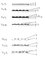
- the method comprises providing a large-area substrate 1 and depositing a first semiconductor, metal, or TCO (Transparent Conductive Oxide) layer 2 (or a combination of a plurality of layers including one or more of said materials) on a surface of the substrate 1 as illustrated in Fig. 1a .
- the layer 2 is deposited e.g. by an evaporation or sputtering method in a vacuum atmosphere.
- a patterned mask layer 3 is printed on top of the first layer 2.
- the mask layer 3 consists of a phase-change material, e.g. wax, which may be deposited in an inkjet printing method.
- the phase-change material has the ability to change in phase from a liquid to a solid state upon contact with the substrate 1.
- the wax layer 3 forms an inverse pattern of the structure to be deposited.
- the structure may be any structure, e.g. a line- and/or grid-like structure, a structure having covered areas and non-covered areas.
- the structure improves the current distribution in an organic electronic device.
- the coated areas provide lines of increased current flow rates.
- a second semiconductor, metal, and/or TCO (Transparent Conductive Oxide; e.g. ITO - Indium Tin Oxide) layer 4 is deposited on top of the mask layer 3 and on top of the first layer 2 where the first layer is not protected by the phase-change masking material 3.
- the second material is deposited e.g. by an evaporation or sputtering method in a vacuum atmosphere.
- the second layer 4 may be of the same material or a material different from the first layer 2.
- a layer system 4 of two or a plurality of layers comprising one or a plurality of semiconductor layers, metal layers, and/or TCO (Transparent Conductive Oxide) layers may be deposited in the step illustrated in Fig. 1c .
- TCO Transparent Conductive Oxide
- phase-change material 3 is removed from the first layer 2.
- a second patterned semiconductor, metal, or TCO (Transparent Conductive Oxide, e.g. ITO - Indium Tin Oxide) layer structure 5 is left on top of the first layer 2 in the areas that had not been covered by the phase-change material.
- the result is a patterned/structured semiconductor, metal, or TCO (Transparent Conductive Oxide) layer 5.
- FIG. 2a to 2c Another embodiment of the invention is illustrated in Figs. 2a to 2c .
- a substrate 1 is provided, and a layer of a phase-change material 3 is deposited directly on the surface of the substrate 1.
- the phase-change material 3 is deposited by using an inkjet printing method.
- the phase-change material layer 3 is patterned to form a structure on the surface of the substrate 1 which is inverse to the line- and/or grid-like structure of an electrode of an organic electronic device to be formed.
- the first layer 4 is deposited on top of the phase-change material layer 3 and, where the surface of the substrate 1 is not protected by the phase-change material, directly on the surface of the substrate1.
- a layer system 4 of two or a plurality of layers comprising one or a plurality of semiconductor layers, metal layers, and/or TCO (Transparent Conductive Oxide) layers may be deposited in the step illustrated in Fig. 2b .
- phase-change material 3 and the metal material 4 deposited on top of the phase-change material 3 are removed from the substrate 1. Thereby, a patterned semiconductor, metal, or TCO (Transparent Conductive Oxide) layer 5 (line- or grid-like) is left directly on the surface of the substrate 1 forming a first electrode of an organic electronic device.
- TCO Transparent Conductive Oxide
Landscapes
- Engineering & Computer Science (AREA)
- Manufacturing & Machinery (AREA)
- Electroluminescent Light Sources (AREA)
Abstract


Description
- The present invention relates to a method of coating a substrate, comprising the steps of: a) providing a substrate having at least one surface to be coated; and b) depositing a shadow mask on said at least one surface of said substrate by using a printing method. Furthermore, the invention relates to a coating installation comprising: a printing tool for printing a shadow mask on a surface of a substrate; and a process chamber for arranging said substrate having said printed shadow mask deposited on said surface in said process chamber.
- Large-area electronic devices usually include an optoelectronic layer for emitting light, e.g. an organic light emitting layer and one or a plurality of layers forming electrodes. An example for a large-area electronic device is an organic electronic device or an OLED (organic light emitting diode) display.
- In order to control the light emission of the single display pixels, the electrode covering the entire area of the display is patterned. Usually, shadow masks are used for patterning the layers forming a first electrode of an organic electronic device, or photolithographic methods are applied. However, the use of shadow masks is expensive and the quality of the pattern decreases with an increasing number of coating processes due to the deposition of coating material on the shadow mask. Therefore, the shadow mask has to be cleaned and exchanged intermittently. Photolithographic procedures, on the other hand, require a lot of equipment and a plurality of process steps and thus involve high costs.
- Consequently, efforts have been made to provide processes of manufacturing a structured or patterned electrode which still have a high throughput, but are more cost-efficient than conventional processes.
- One of these methods is disclosed in
document EP 1 251 398 A2 , wherein a phase-change masking material is deposited on a surface of a substrate. Subsequently, the substrate or the thin film is etched resulting in a removal of material not protected by the phase-change masking material. After the etching step the masking material is removed. - The publication "Printing Methods and Materials for Large-Area Electronic Devices", Proceedings of the IEEE, Vol. 93, No.8, August 2005 by Chabincy, M. L., et al., refers to printing methods for the fabrication of active matrix thin-film transistor backplanes, wherein a printer is used to deposit all the materials of a circuit in a desired pattern directly. Alternatively, direct writing of a resist is disclosed in order to form a patterned etch mask.
- It is an object of the present invention to propose a coating method and a coating installation for depositing a patterned electrode of a large-area electronic device on a substrate, wherein the method and installation result in a reduced number of process steps and have a high throughput.
- This object is achieved by the provision of a coating method according to
claim 1 and a coating installation according to claim 11. The dependent claims contain features of preferred embodiments of the invention. - A method of coating a substrate comprises the steps of: a) providing a substrate having at least one surface to be coated; and b) depositing a patterned mask layer on said at least one surface of said substrate by using a printing method. The method is characterized by a further process step c) of depositing a layer of coating material on said surface of said substrate having said patterned mask deposited thereon.
- The new idea in the method according to the invention is to provide a coating in a vacuum atmosphere after the shadow mask has been deposited on the substrate. The coating material is a semiconductor material or a TCO (Transparent Conductive Oxide) layer, e.g. an ITO coating material, or a metal layer, and may be deposited particularly by using evaporation or sputtering in a vacuum atmosphere.
- The present invention provides a more simple process and thus a reduction of costs of a patterning process in the production of electrodes of OLED devices for the emission of light. The method provides for a reduction of the number of process steps. Furthermore, it is not necessary to use shadow masks for providing a patterned electrode layer on a substrate.
- In a preferred embodiment of the invention the coating material deposited on said surface of said substrate in said step c) comprises a material including a semiconductor material, a metal material, and/or a TCO (Transparent Conductive Oxide; e.g. ITO - Indium Tin Oxide) material.
- Said step c) of depositing a layer of coating material on the surface of the substrate may include depositing a layer comprising one or a stack of layers including a semiconductor layer, a metal layer, and/or a TCO (Transparent Conductive Oxide) layer. The layers of the stack of layers may be regarded as sub-layers of the layer deposited a on the surface of the substrate.
- It is preferred that said step c) of depositing a layer of coating material on said surface of said substrate includes using a sputtering method, an evaporation method, a plasma coating method, a CVD method, and/or a PVD method.
- Particularly, the method of coating a substrate is carried out for providing a patterned electrode of an LED (light emitting diode) display, particularly of an organic electronic device, on said substrate.
- In a preferred embodiment of the invention said method step a) comprises a step of depositing a first layer of coating material on said at least one surface to be coated. Said first layer of coating material may be a semiconductor material layer, a metal layer, and/or a TCO (Transparent Conductive Oxide; e.g. ITO - Indium Tin Oxide) coating material layer. The same or a different material may be used to deposit the first layer and the layer of coating material deposited in process step c).
- In another embodiment of the invention the method comprises a step of providing an optoelectronic device layer for the emission of light on said substrate.
- In another embodiment of the invention said process step b) comprises using a printing method selected from inkjet printing, screen printing, porous printing, pad printing, etc. The most suitable printing method may be selected for a particular application.
- It is preferred that said method step b) includes printing a phase-change material, e.g. wax, and/or a lift-off material on said surface in order to form said patterned mask. A phase-change material has the ability to change in phase from a liquid to a solid state upon contact with the substrate. The mask layer forms an inverse pattern of the structure to be deposited. The structure may be any structure, e.g. a line- and/or grid-like structure, a structure having covered areas and non-covered areas. The covered areas may be separated from each other, i.e. they may be printed without establishing any connections between the covered areas. In other words, the covered areas may form "islands" on top of the surface. The mask layer may be deposited in a protective atmosphere, e.g. in an inert gas atmosphere, or in a vacuum atmosphere. The printing device for providing the phase-change material layer may be integrated in a process chamber, wherein other coating processes may be carried out, or in a chamber separate from the coating chamber.
- In a preferred embodiment of the invention said method includes a further process step d) removing said mask material from said substrate. This material must have the property to be easily removable from the surface of the substrate. In the end the second patterned semiconductor material, metal, and/or TCO (Transparent Conductive Oxide) layer structure (step c) is arranged on top of the first layer (step a) in the areas that had not been protected by the phase-change material.
- The object of the invention is also achieved by the provision of a coating installation comprising: a printing tool for printing a patterned mask on a surface of a substrate; and a process chamber for arranging said substrate having said printed patterned mask deposited on the surface thereof in said process chamber. Furthermore, the coating installation comprises coating tools provided in said process chamber for depositing a coating layer on said surface of said substrate arranged in said process chamber; wherein said coating tools comprise a coating material source providing said coating material to be deposited on said surface of said substrate.
- In a preferred embodiment said coating material source is a semiconductor, a metal, a TCO (Transparent Conductive Oxide), and/or an ITO (indium tin oxide) material source.
- In another preferred embodiment of the invention said coating tools comprise sputter coating equipment, evaporation equipment, CVD coating equipment and/or PVD coating equipment.
- Said printing tool for printing said patterned mask may include an inkjet printer, a screen printer, and/or a pad printing equipment.
- Particularly, said coating equipment further comprises tools for removing said shadow mask material from said surface of said substrate.
- Said coating equipment may include a further coating station comprising coating tools for depositing an LED (light emitting diode) layer system on said substrate, particularly a layer system of an organic electronic device.
- Particularly, said coating equipment further comprises tools for removing said patterned mask material from said surface of said substrate
- The features described above are meant to be protected by themselves or in any combination with the described method and/or device features.
- Further objects and advantages result from the following description of specific embodiments. The figures show:
- Fig. 1a to 1d
- a first embodiment of a method according to the present invention; and
- Fig. 2a to 2c
- a second embodiment of a method according to the present invention.
- The embodiments disclosed in this application refer to methods of depositing a patterned first electrode of an organic electronic device on a substrate. The substrate on which the electrode is deposited may be the carrier of the layer system deposited thereon. It may or may not comprise e. g. one or a plurality of light emitting layers, functional and/or protective layers, barrier layers, etc. The light emitting layer or layer stack may be deposited on top of the patterned first electrode.
- In the first embodiment of the invention the method comprises providing a large-
area substrate 1 and depositing a first semiconductor, metal, or TCO (Transparent Conductive Oxide) layer 2 (or a combination of a plurality of layers including one or more of said materials) on a surface of thesubstrate 1 as illustrated inFig. 1a . Thelayer 2 is deposited e.g. by an evaporation or sputtering method in a vacuum atmosphere. - In a second process step illustrated in
Fig. 1b a patternedmask layer 3 is printed on top of thefirst layer 2. Themask layer 3 consists of a phase-change material, e.g. wax, which may be deposited in an inkjet printing method. The phase-change material has the ability to change in phase from a liquid to a solid state upon contact with thesubstrate 1. Thewax layer 3 forms an inverse pattern of the structure to be deposited. The structure may be any structure, e.g. a line- and/or grid-like structure, a structure having covered areas and non-covered areas. The structure improves the current distribution in an organic electronic device. The coated areas provide lines of increased current flow rates. - In a third process step (
Fig. 1c ) a second semiconductor, metal, and/or TCO (Transparent Conductive Oxide; e.g. ITO - Indium Tin Oxide)layer 4 is deposited on top of themask layer 3 and on top of thefirst layer 2 where the first layer is not protected by the phase-change masking material 3. The second material is deposited e.g. by an evaporation or sputtering method in a vacuum atmosphere. Thesecond layer 4 may be of the same material or a material different from thefirst layer 2. Instead of a singlesecond layer 4, alayer system 4 of two or a plurality of layers comprising one or a plurality of semiconductor layers, metal layers, and/or TCO (Transparent Conductive Oxide) layers may be deposited in the step illustrated inFig. 1c . - Afterwards, in a process step indicated in
Fig. 1d the phase-change material 3 is removed from thefirst layer 2. A second patterned semiconductor, metal, or TCO (Transparent Conductive Oxide, e.g. ITO - Indium Tin Oxide)layer structure 5 is left on top of thefirst layer 2 in the areas that had not been covered by the phase-change material. The result is a patterned/structured semiconductor, metal, or TCO (Transparent Conductive Oxide)layer 5. - Another embodiment of the invention is illustrated in
Figs. 2a to 2c . - In a first step a
substrate 1 is provided, and a layer of a phase-change material 3 is deposited directly on the surface of thesubstrate 1. The phase-change material 3 is deposited by using an inkjet printing method. The phase-change material layer 3 is patterned to form a structure on the surface of thesubstrate 1 which is inverse to the line- and/or grid-like structure of an electrode of an organic electronic device to be formed. - Afterwards, in a subsequent process step illustrated in
Fig. 2b thefirst layer 4 is deposited on top of the phase-change material layer 3 and, where the surface of thesubstrate 1 is not protected by the phase-change material, directly on the surface of the substrate1. Instead of a singlefirst layer 4, alayer system 4 of two or a plurality of layers comprising one or a plurality of semiconductor layers, metal layers, and/or TCO (Transparent Conductive Oxide) layers may be deposited in the step illustrated inFig. 2b . - Afterwards, the phase-
change material 3 and themetal material 4 deposited on top of the phase-change material 3 are removed from thesubstrate 1. Thereby, a patterned semiconductor, metal, or TCO (Transparent Conductive Oxide) layer 5 (line- or grid-like) is left directly on the surface of thesubstrate 1 forming a first electrode of an organic electronic device. - In this way the number of process steps may be reduced. Furthermore, it is not necessary to use a shadow mask for providing a patterned electrode layer on a substrate.
Claims (16)
- A method of coating a substrate (1), comprising the steps of: a) providing a substrate (1) having at least one surface to be coated; and b) depositing a patterned mask layer (3) on said at least one surface of said substrate (1) by using a printing method,
characterized by
a further process step c) of depositing a layer (4) of coating material on said surface of said substrate (1) having said patterned mask layer (3) deposited thereon. - The method of coating a substrate according to claim 1,
characterized in that
said layer of coating material (4) deposited on said surface of said substrate (1) in step c) comprises a material including a semiconductor material, a metal material, and/or a TCO (Transparent Conductive Oxide) material. - The method of coating a substrate (1) according to claim 1 or 2,
characterized in that
said step c) of depositing a layer (4) of coating material on said surface of said substrate (1) includes depositing a layer (4) comprising one or a stack of layers including a semiconductor layer, a metal layer, and/or a TCO (Transparent Conductive Oxide) layer. - The method of coating a substrate (1) according to any of the previous claims,
characterized in that
said step c) of depositing a layer of coating material (4) on said surface of said substrate includes using a sputtering method, an evaporation method, a plasma coating method, a CVD method, and/or a PVD method. - The method of coating a substrate (1) according to any of the previous claims,
characterized in that
said method is carried out for providing a patterned electrode of an organic electronic device on said substrate (1). - The method of coating a substrate (1) according to any of the previous claims,
characterized in that
said method step a) comprises a step of depositing a first layer (2) of coating material on said at least one surface of the substrate (1) to be coated. - The method of coating a substrate (1) according to any of the previous claims,
characterized in that
said method comprises a step of providing an optoelectronic device layer for the emission of light on said substrate. - The method of coating a substrate (1) according to any of the previous claims,
characterized in that
said process step b) comprises using a printing method selected from inkjet printing, screen printing, porous printing, pad printing, etc, or a combination of such printing methods. - The method of coating a substrate (1) according to any of the previous claims,
characterized in that
said method step b) includes printing a phase-change material and/or a lift-off material on said surface in order to form said patterned mask (3). - The method of coating a substrate (1) according to any of the previous claims,
characterized in that
said method includes a further process step d) of removing said mask material (3) from said substrate (1). - A coating installation comprising:a printing tool for printing a patterned mask (3) on a surface of a substrate; anda process chamber for arranging said substrate (1) having said patterned mask deposited on the surface thereof in said process chamber;characterized in that
said coating installation further comprises coating tools provided in said process chamber for depositing a coating layer (4) on said surface of said substrate (1) arranged in said process chamber; wherein said coating tools comprise a coating material source providing said coating material (4) to be deposited on said surface of said substrate (1). - The coating installation according to claim 11,
characterized in that
said coating material source is a metal material source and/or a semiconductor material, a metal, and/or a TCO (Transparent Conductive Oxide) material source. - The coating installation according to claim 11 or 12,
characterized in that
said coating tools comprise sputter coating equipment, evaporation equipment, CVD coating equipment and/or PVD coating equipment. - The coating installation according to any of the previous claims 11 to 13,
characterized in that
said printing tool for printing said patterned mask (3) includes an inkjet printer, a screen printer, and/or a pad printing equipment. - The coating installation according to any of the previous claims 11 to 14,
characterized in that
said coating equipment includes a further coating station comprising coating tools for depositing an organic electronic device on said substrate (1), particularly comprising a layer system including at least an organic material layer. - The coating installation according to any of the previous claims 11 to 15,
characterized in that
said coating equipment further comprises tools for removing said patterned mask material (3) from said surface of said substrate (1).
Priority Applications (1)
| Application Number | Priority Date | Filing Date | Title |
|---|---|---|---|
| EP08101176A EP2086033A1 (en) | 2008-01-31 | 2008-01-31 | Method of coating a substrate and coating installation |
Applications Claiming Priority (1)
| Application Number | Priority Date | Filing Date | Title |
|---|---|---|---|
| EP08101176A EP2086033A1 (en) | 2008-01-31 | 2008-01-31 | Method of coating a substrate and coating installation |
Publications (1)
| Publication Number | Publication Date |
|---|---|
| EP2086033A1 true EP2086033A1 (en) | 2009-08-05 |
Family
ID=39472818
Family Applications (1)
| Application Number | Title | Priority Date | Filing Date |
|---|---|---|---|
| EP08101176A Withdrawn EP2086033A1 (en) | 2008-01-31 | 2008-01-31 | Method of coating a substrate and coating installation |
Country Status (1)
| Country | Link |
|---|---|
| EP (1) | EP2086033A1 (en) |
Cited By (1)
| Publication number | Priority date | Publication date | Assignee | Title |
|---|---|---|---|---|
| WO2012160468A1 (en) * | 2011-05-23 | 2012-11-29 | Koninklijke Philips Electronics N.V. | Fabrication apparatus for fabricating a patterned layer |
Citations (6)
| Publication number | Priority date | Publication date | Assignee | Title |
|---|---|---|---|---|
| EP1251398A2 (en) | 2001-04-19 | 2002-10-23 | Xerox Corporation | Method for printing etch masks using phase-change materials |
| US20050059193A1 (en) * | 2003-09-11 | 2005-03-17 | Nobuhide Yoneya | Method for forming metal single-layer film, method for forming wiring, and method for producing field effect transistors |
| US20070111144A1 (en) * | 2005-11-17 | 2007-05-17 | Semiconductor Energy Laboratory Co., Ltd. | Display device and manufacturing method of the same |
| US20070148813A1 (en) * | 2005-12-28 | 2007-06-28 | Seiko Epson Corporation | Electric device, method of manufacturing electric device and electric apparatus |
| US20070190234A1 (en) * | 2006-02-15 | 2007-08-16 | Eastman Kodak Company | Common shadow mask for OLED lighting display |
| WO2008012080A1 (en) * | 2006-07-28 | 2008-01-31 | Leonhard Kurz Stiftung & Co. Kg | Method for producing at least one component and component |
-
2008
- 2008-01-31 EP EP08101176A patent/EP2086033A1/en not_active Withdrawn
Patent Citations (6)
| Publication number | Priority date | Publication date | Assignee | Title |
|---|---|---|---|---|
| EP1251398A2 (en) | 2001-04-19 | 2002-10-23 | Xerox Corporation | Method for printing etch masks using phase-change materials |
| US20050059193A1 (en) * | 2003-09-11 | 2005-03-17 | Nobuhide Yoneya | Method for forming metal single-layer film, method for forming wiring, and method for producing field effect transistors |
| US20070111144A1 (en) * | 2005-11-17 | 2007-05-17 | Semiconductor Energy Laboratory Co., Ltd. | Display device and manufacturing method of the same |
| US20070148813A1 (en) * | 2005-12-28 | 2007-06-28 | Seiko Epson Corporation | Electric device, method of manufacturing electric device and electric apparatus |
| US20070190234A1 (en) * | 2006-02-15 | 2007-08-16 | Eastman Kodak Company | Common shadow mask for OLED lighting display |
| WO2008012080A1 (en) * | 2006-07-28 | 2008-01-31 | Leonhard Kurz Stiftung & Co. Kg | Method for producing at least one component and component |
Non-Patent Citations (1)
| Title |
|---|
| CHABINCY, M. L.: "Printing Methods and Materials for Large-Area Electronic Devices", PROCEEDINGS OF THE IEEE, vol. 93, no. 8, August 2005 (2005-08-01), XP011136594, DOI: doi:10.1109/JPROC.2005.851492 |
Cited By (4)
| Publication number | Priority date | Publication date | Assignee | Title |
|---|---|---|---|---|
| WO2012160468A1 (en) * | 2011-05-23 | 2012-11-29 | Koninklijke Philips Electronics N.V. | Fabrication apparatus for fabricating a patterned layer |
| CN103548174A (en) * | 2011-05-23 | 2014-01-29 | 皇家飞利浦有限公司 | Fabrication equipment for fabricating patterned layers |
| CN103548174B (en) * | 2011-05-23 | 2016-09-28 | Oled工厂有限责任公司 | Fabrication apparatus and method for fabricating patterned layer and electrical device |
| US9472787B2 (en) | 2011-05-23 | 2016-10-18 | Oledworks Gmbh | Fabrication apparatus for fabricating a patterned layer |
Similar Documents
| Publication | Publication Date | Title |
|---|---|---|
| CN114514626B (en) | OLED panel with inorganic pixel encapsulation barrier layer | |
| CN115241232A (en) | Conductive oxide overhang structures for OLED devices | |
| JP7536182B2 (en) | Metal protrusions for advanced patterning | |
| US7476278B2 (en) | Roll to roll manufacturing of organic solar modules | |
| EP1232531B1 (en) | Method for patterning devices | |
| WO2023014897A1 (en) | Descending etching resistance in advanced substrate patterning | |
| US20130084666A1 (en) | Method for manufacturing light emitting device | |
| US20230389343A1 (en) | Oled anode structures including amorphous transparent conducting oxides and oled processing method comprising the same | |
| EP2251906B1 (en) | Method of fabricating organic light emitting diode display | |
| EP2609641B1 (en) | Self-aligned coverage of opaque conductive areas | |
| WO2022051004A1 (en) | Inorganic silicon-containing overhang structures of oled sub-pixels | |
| EP2086033A1 (en) | Method of coating a substrate and coating installation | |
| US20050282368A1 (en) | Mask, method for producing the same, deposition method, electronic device, and electronic apparatus | |
| KR20180105713A (en) | Shadow mask with tapered apertures formed by dual electroforming using positive / negative photoresists | |
| KR101722936B1 (en) | Manufacturing method of flexible display device | |
| CN112687825A (en) | Preparation method of OLED display panel and OLED display panel | |
| EP2177644A1 (en) | Coating of masked substrates | |
| US20100092658A1 (en) | Coating of masked substrates | |
| EP2784840B1 (en) | Method of manufacturing an organic device | |
| US20260047330A1 (en) | Advanced patterning oled structure for anode protection | |
| CN103855084B (en) | The method for manufacturing organic light-emitting display device | |
| US20250311585A1 (en) | Patterning overhang as touch electrodes | |
| US20250248220A1 (en) | Venting hole on passivation layer on top of gap-fill | |
| WO2026029891A1 (en) | Device protected layer for oled advanced patterning | |
| KR20000072485A (en) | Method for manufacturing shadow mask for micro display OLED |
Legal Events
| Date | Code | Title | Description |
|---|---|---|---|
| PUAI | Public reference made under article 153(3) epc to a published international application that has entered the european phase |
Free format text: ORIGINAL CODE: 0009012 |
|
| 17P | Request for examination filed |
Effective date: 20080215 |
|
| AK | Designated contracting states |
Kind code of ref document: A1 Designated state(s): AT BE BG CH CY CZ DE DK EE ES FI FR GB GR HR HU IE IS IT LI LT LU LV MC MT NL NO PL PT RO SE SI SK TR |
|
| AX | Request for extension of the european patent |
Extension state: AL BA MK RS |
|
| AKX | Designation fees paid | ||
| STAA | Information on the status of an ep patent application or granted ep patent |
Free format text: STATUS: THE APPLICATION IS DEEMED TO BE WITHDRAWN |
|
| 18D | Application deemed to be withdrawn |
Effective date: 20100206 |
|
| REG | Reference to a national code |
Ref country code: DE Ref legal event code: 8566 |