EP2084524B1 - Magnetic sensor apparatus for detecting defects - Google Patents
Magnetic sensor apparatus for detecting defects Download PDFInfo
- Publication number
- EP2084524B1 EP2084524B1 EP07793409.9A EP07793409A EP2084524B1 EP 2084524 B1 EP2084524 B1 EP 2084524B1 EP 07793409 A EP07793409 A EP 07793409A EP 2084524 B1 EP2084524 B1 EP 2084524B1
- Authority
- EP
- European Patent Office
- Prior art keywords
- line
- power
- magnetic field
- arrayed
- magneto
- Prior art date
- Legal status (The legal status is an assumption and is not a legal conclusion. Google has not performed a legal analysis and makes no representation as to the accuracy of the status listed.)
- Active
Links
Images







Classifications
-
- G—PHYSICS
- G01—MEASURING; TESTING
- G01N—INVESTIGATING OR ANALYSING MATERIALS BY DETERMINING THEIR CHEMICAL OR PHYSICAL PROPERTIES
- G01N27/00—Investigating or analysing materials by the use of electric, electrochemical, or magnetic means
- G01N27/72—Investigating or analysing materials by the use of electric, electrochemical, or magnetic means by investigating magnetic variables
- G01N27/82—Investigating or analysing materials by the use of electric, electrochemical, or magnetic means by investigating magnetic variables for investigating the presence of flaws
-
- G—PHYSICS
- G01—MEASURING; TESTING
- G01N—INVESTIGATING OR ANALYSING MATERIALS BY DETERMINING THEIR CHEMICAL OR PHYSICAL PROPERTIES
- G01N27/00—Investigating or analysing materials by the use of electric, electrochemical, or magnetic means
- G01N27/72—Investigating or analysing materials by the use of electric, electrochemical, or magnetic means by investigating magnetic variables
- G01N27/82—Investigating or analysing materials by the use of electric, electrochemical, or magnetic means by investigating magnetic variables for investigating the presence of flaws
- G01N27/90—Investigating or analysing materials by the use of electric, electrochemical, or magnetic means by investigating magnetic variables for investigating the presence of flaws using eddy currents
- G01N27/9006—Details, e.g. in the structure or functioning of sensors
-
- G—PHYSICS
- G01—MEASURING; TESTING
- G01N—INVESTIGATING OR ANALYSING MATERIALS BY DETERMINING THEIR CHEMICAL OR PHYSICAL PROPERTIES
- G01N27/00—Investigating or analysing materials by the use of electric, electrochemical, or magnetic means
- G01N27/72—Investigating or analysing materials by the use of electric, electrochemical, or magnetic means by investigating magnetic variables
-
- G—PHYSICS
- G01—MEASURING; TESTING
- G01R—MEASURING ELECTRIC VARIABLES; MEASURING MAGNETIC VARIABLES
- G01R33/00—Arrangements or instruments for measuring magnetic variables
- G01R33/02—Measuring direction or magnitude of magnetic fields or magnetic flux
- G01R33/06—Measuring direction or magnitude of magnetic fields or magnetic flux using galvano-magnetic devices
- G01R33/09—Magnetoresistive devices
Definitions
- the divider 120 controls the phases of the ACs that are respectively distribut ed to the first coils 131 a and 131b in consideration of an angle between the conductive plates 133a and 133b.
- a predetermined difference exists between the pha ses of a line or surface current induced on one of the conductive plates 133a and 133b and a line or surface current inducted on the other one of the conductive plates 133a an d 133b.
Landscapes
- Chemical & Material Sciences (AREA)
- Physics & Mathematics (AREA)
- General Physics & Mathematics (AREA)
- Health & Medical Sciences (AREA)
- Chemical Kinetics & Catalysis (AREA)
- Electrochemistry (AREA)
- Life Sciences & Earth Sciences (AREA)
- Analytical Chemistry (AREA)
- Biochemistry (AREA)
- General Health & Medical Sciences (AREA)
- Immunology (AREA)
- Pathology (AREA)
- Condensed Matter Physics & Semiconductors (AREA)
- Investigating Or Analyzing Materials By The Use Of Magnetic Means (AREA)
Description
- The present invention relates to a magnetic sensor array and an apparatus for d etecting defects of a ferromagnetic structure, a paramagnetic structure, and a structure formed of ferromagnetic and paramagnetic substances using the magnetic sensor array
- A non-destructive inspection method using a magnetic phenomenon is useful to detect a surface defect of a structure, a near surface defect of the structure, or an inter nal defect of the structure. The non-destructive inspection method can be used to det ect a defect of a large plant or structure used for nuclear power generation, a thermal p ower plant, chemical industry, etc.
- A paramagnetic substance, such as an aluminum alloy or stainless steel, is use d for airplanes or nuclear power generation equipment. A non-destructive inspection method using magneto-optical effects has attracted attention as a method of measuring damage to a paramagnetic substance. In particular, a Magneto-Optical eddy current Imager (MOI) has been developed by PRI R&D Co. to non-destructively detect the defe cts of an airplane. An image indicating a surface fatigue crack and erosion of a param agnetic substance, a defect of a near surface of the paramagnetic substance, etc., can be obtained using the MOI.
-
FIG. 1A illustrates a surface fatigue crack in an aluminum alloy plate, which is a paramagnetic substance, wherein the surface fatigue crack is detected using an MOI.FIG. 1 B illustrates a surface crack in austenite stainless steel formed of a mixture of ferr omagnetic and paramagnetic substances, wherein the surface crack is detected using a n MOI. InFIG. 1B , the surface crack and a martensite area are illustrated in the auste nite stainless steel. - If an object that is to be measured is a paramagnetic substance as shown in Fl G. 1A, surface cracks that are indistinguishable to the naked eye can be easily detected from the object using the MOI. However, if an object that is to be measured is a para magnetic structure locally mixed with a ferromagnetic substance as shown in
FIG. 1 B , it is very difficult to detect surface cracks in the object using the MOI. - Also, if the MOI is used, it is difficult to quantitatively evaluate the leakage flux g enerated by the dispersion of an induced current around the surface cracks. In other words, since the MOI provides only image data regarding the surface cracks as shown in
FIG. 1A or 1B , it is difficult to quantitatively evaluate actual shapes, sizes, or the like of the surface cracks. In addition, the detected results may be differently interpreted according to the knowledge or skill of an inspector. - The present invention provides a defect detection apparatus for quantitatively analyzing surface defects, near surface defects, and internal surface defects of a ferromagnetic structure, a paramagnetic structure, or a structure formed of a mixture of ferromagnetic and paramagnetic substances, and a magnetic sensor array used in the defect detection apparatus.
- The present invention is more particularly defined in claim 1.
- The magneto-electric converter can comprise hall sensors arrayed in M rows and N lines; M first power lines; M second power lines; and N first output lines, wherein first power terminals of hall sensors belonging to an mth (where m is a natural number from "1" to "M") row are connect
- According to a further embodiment of the present invention, the magneto-electric converter comprises a hall effect material coated on a substrate and having a prede termined size; M first power terminals formed on a first side of the hall effect material; M first power switches respectively connected to the M first power terminals; M second p ower terminals formed on a second side of the hall effect material; M second power swit ches respectively connected to the M second power terminals; N first output terminals f ormed on a third side of the hall effect material; and N second output terminals formed on a fourth side of the hall effect material.
- According to the present invention, surface defects, near surface defects, and in ternal defects of a ferromagnetic structure, a paramagnetic structure, or a structure for med of a mixture of ferromagnetic and paramagnetic substances can be detected. Als o, if a defect detection apparatus of the present invention is used, defects such as surfa ce cracks in an object that is to be measured can be quantitatively analyzed.
-
-
FIG. 1A illustrates a surface fatigue crack in an aluminum alloy plate, which is a paramagnetic substance, wherein the surface fatigue crack is detected using a Magnet o-Optical eddy current Imager (MOI). -
Figure 1 B illustrates a surface crack in austenite stainless steel formed of a mixtur e of ferromagnetic and paramagnetic substances, wherein the surface crack is detected using an MOI. -
FIG. 2 illustrates an apparatus for detecting defects of a ferromagnetic structure, a paramagnetic structure, or a structure formed of a mixture of ferromagnetic and para magnetic substances, according to an embodiment of the present invention. -
FIG. 3A illustrates an inducted current applier illustrated inFIG. 2 in detail. -
FIG. 3B illustrates arrangements of conductive plates. -
FIG. 3C illustrates a combined structure of a first coil, a core, and a conductive plate. -
FIG. 4A illustrates a hall sensor and a signal processor. -
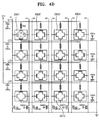
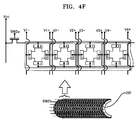
FIGS. 4B through 4I illustrate hall sensor arrays according to embodiments of th e present invention. -
FIG. 4J illustrates a magneto-resistive sensor array according to an embodiment of the present invention. -
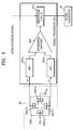
FIG. 5 is a detailed block diagram of a signal processor illustrated inFIG. 2 , acc ording to an embodiment of the present invention. -
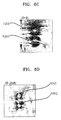
FIGS. 6A through 6D illustrate surface cracks of an object formed of a mixture o f ferromagnetic and paramagnetic substances, which are detected by using a defect det ection apparatus of the present invention. -
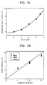
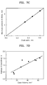
FIGS. 7A through 7D illustrate the detection results ofFIG. 6 , which are quantita tively analyzed. -
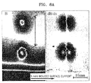
FIG. 8A illustrates surface cracks of a paramagnetic structure (aluminum alloy) detected using a defect detection apparatus of the present invention. -
FIG. 8B illustrates surface cracks of a ferromagnetic structure (carbon steel) det ected using the defect detection apparatus of the present invention. - A preferred embodiment of the present invention will now be described with refe rence to the attached drawings.
-
FIG. 2 illustrates an apparatus for detecting defects of a ferromagnetic structure, a paramagnetic structure, or a structure formed of a mixture of ferromagnetic and para magnetic substances, according to an embodiment of the present invention. Anobject 60 that is to be measured, an inducedcurrent applier 10, a magneto-electric converter 20, asignal processor 30, asignal converter 40, and adata processor 50 are shown inFIG. 2 . - If the induced current applier 10 applies a line or
surface current 123 to theobje ct 60, an induced line orsurface current 153 is induced in theobject 60. If the induced line orsurface current 153 is dispersed around asurface crack 601 as shown inFIG. 2 , i.e., paths of the induced line orsurface current 153 is changed like 141a and 141b, magnetic fields surface crack 601 perpendicula r to a surface of theobject 60. If theobject 60, which is a paramagnetic substance, is I ocally mixed with aferromagnetic substance 650, amagnetic field 190 is generated by r esidual magnetization of theferromagnetic substance 650. Themagnetic fields surface crack 601, may be hereinafter called alternating curre nt (AC)magnetic fields magnetic field 190 formed by the ferromagnetic substance 650 may be hereinafter called a direct current (DC)magnetic field 190. In the present invention, thesignal processor 30 can separate the components o f the ACmagnetic fields FIG. 5 . -
FIG. 3A illustrates the inductedcurrent applier 10 illustrated inFIG. 2 in detail. Referring toFIG. 3A , the inducedcurrent applier 10 includes an AC power source supplier 110, adivider 120, one or morefirst coils more cores 132a and 132b, and one or moreconductive plates cores plates FIG. 3A , theconductive plate 133a may be disposed so that a portion thereof is adhered to theobject 60. - The AC
power source supplier 110 generates an AC that is supplied to thefirst coils divider 120. Thecores first coils conductive plates conductive plates conductive plates conductive plates cores con ductive plates FIG. 2 , induced by the AC to theobject 60. If the line or surface current 123 is applied toth e object 60, a magnetic field is generated by leakage flux around thesurface crack 60 1, anear surface crack 603, or aninternal crack 602 of theobject 60. - As shown in
FIG. 3A , the ACpower source supplier 110 includes afrequency g enerator 111 and apower amplifier 112. Thefrequency generator 111 generates the AC having a predetermined frequency, and thefrequency generator 111 can also outpu t a synchronizing signal to thesignal processor 30 to control an operation of thesignal p rocessor 30 as described later in detail with reference toFIG. 5 . The power amplifier 1 12 amplifies the power of the AC generated by thefrequency generator 111, and the A Cpower source supplier 110 may supply ACs having various waveforms such as a sine wave, a half-rectifying wave, a pulse wave, etc. The AC power source supplier 110 c an also vary the frequency of the AC depending on the depth to be measured from the surface of theobject 60. For example, if thesurface crack 601 is to be detected, the A Cpower source supplier 110 may use a low or high frequency. If the nearsurface cra ck 603 or theinternal crack 602 is to be detected, the AC power source supplier 110 m ay use a low frequency based on the physical principle that a low frequency signal can deeply infiltrate theobject 60. - If the induced
current applier 10 only includes one first coil, one core, and one c onductive plate, thedivider 120 is not needed. However, a plurality of first coils, cores, and conductive coils can be used, and thus, as shown in the present embodiment, thefirst coils cores conductive plates 133a and 133b may be used to detect cracks of theobject 60 from various angles. In this case , thedivider 120 divides the AC output from the ACpower source supplier 110 so as to distribute the AC to thefirst coils divider 120 control s the phases of the ACs that are respectively distributed to thefirst coils - In detail, the
divider 120 controls the phases of the ACs that are respectively distribut ed to thefirst coils conductive plates conductive plates conductive plates 133a and 133b. -
FIG. 3B illustrates arrangements of theconductive plates FIG. 3B , portions of theconductive plates object 60. An inducted current is dispersed aroundcracks obje ct 60. As shown inFIG. 3B , theconductive plates cracks object 60 in theconductive plates cracks cracks cracks object 60. In the present invention, thec onductive plates cracks conductive plates cracks cracks - However, even if only the
conductive plate 133a is included, the conductive plat e 133a may be rotated in various directions on the surface of theobject 60 to detect thecracks cracks conductive plate 133a is included, as previously described, thedivider 120 is not needed. -
FIG. 3C illustrates a combined structure of afirst coil 131, acore 132, and acon ductive plate 133. Referring toFIG. 3C , thecore 132 includes a plurality of through pa ths 132_1, 132_2, 132_3, and 132_4. If theconductive plate 133 passes the through paths 132_1, 132_2, 132_3, and 132_4, a line or surface current applied to theobject 6 0 may be strengthened. In other words, an area of theconductive plate 133 penetratin g thecore 132 may be increased to strengthen a line or surface current induced on theconductive plate 133. If the line or surface current induced on the conductive plate 13 3 is strengthened, the line or surface current applied to theobject 60 is also strengthen ed. In this case, the strength of a magnetic field by leakage flux generated around a cr ack of theobject 60 is strengthened, and thus, the crack of theobject 60 can be easily detected. In other words, the strength of the magnetic field by the leakage flux generat ed around the crack of theobject 60 can be strengthened, thereby improving a detectio n capability. - The magneto-
electric converter 20 ofFIG. 2 senses the ACmagnetic fields magnetic field 190 that are generated from theobject 60 due t o the line or surface current 153, and the magneto-electric converter 20 generates mag netic field sensing signals corresponding to the strengths of the ACmagnetic fields magnetic field 190. The magneto-electric converter 20 may b e realized using a hall sensor, a hall integrated circuit (IC), a magneto-resistive sensor, or a giant magneto-resistive sensor. The magneto-electric converter 20 will now be de scribed in detail with reference toFIGS. 4A through 4J . -
FIG. 4A illustrates a hall sensor and a signal processor,FIGS. 4B through 4I illu strates hall sensor arrays according to embodiments of the present invention, andFIG. 4J illustrates a magneto-resistive sensor array according to an embodiment of the pres ent invention. - The magneto-
electric converter 20 ofFIG. 2 may include ahall sensor 2001 sho wn inFIG. 4A , the hall sensor array shown inFIGS. 4B through 4I , or the magneto-resis tive sensor array shown inFIG. 4J . - As shown in
FIG. 4A , thehall sensor 2001 includes first and second power termi nals 2001 a and 2001 c and first andsecond output terminals second power terminal 2001c, thehall sensor 2001 outputs magnetic field sensing signal, corresponding to the strength of the magn etic field incident onto thehall sensor 2001, to thesignal processor 30 through the first andsecond output terminals hall sensor 2001, a voltage difference occurs betw een the first andsecond output terminals output terminals electric converter 20 may includ e a hall IC, which is a device onto which a hall sensor and a differential amplifying circui t are integrated. - A single hall sensor can be precisely moved on a plane parallel with the
object 6 0 to sense a magnetic field generated around a crack of theobject 60. In this method, the single hall sensor must be moved so as to precisely scan theobject 60. The mag netic field generated around the crack of theobject 60 may be sensed using a 1-dimen sional magnetic sensor array, a 2-dimensional magnetic sensor array, or a 3-dimension al magnetic sensor array besides a single magnetic sensor. - The hall sensor array shown in
FIG. 4B includes hall sensors, for example, 2101 , 2102, 2103, 2104, and 2115, which are arrayed in M rows and N lines (4 rows and 4 li nes are shown inFIG. 4B , however the present invention is not limited thereto). That i s, the hall sensor array includes M first power lines L11, L21, L31, through LM1, M seco nd power lines L12, L22, L32, through LM2, N first output lines V1+, V2+, V3+, through VN+, and N second output lines V1-, V2-, V3-, through VN-, where N and M are a natur al number. In the present embodiment, for convenience of explanation, 4 first power li nes L11, L21, L31, and L41, 4 second power lines L12, L22, L32, and L42, 4 first output lines V1+, V2+, V3+, and V4+, and 4 second output lines V1-, V2-, V3-, and V4- are ill ustrated. As shown inFIG. 4B , first power terminals a of hall sensors belonging to the mth (where m is a natural number from "1" to "M.") row are connected to a first power lin e Lm1 of the mth row, and second power terminals c of the hall sensors belonging to the mth row are connected to a second power line Lm2 of the mth row. First output termin als d of hall sensors belonging to the nth (where n is a natural number from "1" to "N.") li ne are connected to a first output line Vn+ of the nth line, and second output terminals b of the hall sensors belonging to the nth line are connected to a second output line Vn-of the nth line. A switch SW1 a transmits a first power source voltage Vcc to the first po wer line L11 of the first row, and a switch SW1 b transmits a second power source volta ge Vg to the second power line L12 of the first row. Similarly, a switch SW4a transmits the first power source voltage Vcc to the first power line L41 of the fourth row, and a s witch SW4b transmits the second power source voltage Vg to the secondpower line L4 2 of the fourth row. - If the first power source voltage Vcc is applied to the first power line Lm1 of the mth row, and the second power source voltage Vg is applied to the second power line L m2 of the mth row, the hall sensor arrayed in the mth row and the nth line outputs a magn etic field sensing signal corresponding to the strength of a magnetic field, which is gene rated from the
object 60 and incident onto the hall sensor, through the first and second output lines Vn+ and Vn- of the nth line. For example, if the switches SW1a and SW1b are turned on, thehall sensor 2102 arrayed in the first row and the second line outputs a magnetic field sensing signal corresponding to the strength of a magnetic field incide nt onto thehall sensor 2102 through first and second output lines V2+ and V2- of the se cond line. If the switches SW4a and SW4b are turned on, thehall sensor 2115 arraye d in the fourth row and the third line outputs a magnetic field sensing signal correspondi ng to the strength of a magnetic field incident onto thehall sensor 2115 through first an d second output lines V3+ and V3- of the third line. - The hall sensor array shown in
FIG. 4C is very similar to the hall sensor array sh own inFIG. 4B . However, the pad shapes of terminals a, b, c, and d of the hall sensor s are slightly different. - The hall sensor array shown in
FIG. 4D further includes resistors Rd that are arr ayed in M rows and N lines. As shown inFIG. 4D , a first power terminal a of a hall sen sor arrayed in an mth row and an nth line is connected to a first power line Lm1 of the mt h row through the resistor Rd arrayed in the mth row and the nth line. The operation con ditions of hall sensors arrayed in M rows and N lines can be adjusted to be the same us ing the resistors Rd arrayed in the M row and the N lines. - The hall sensor array of
FIG. 4D further includes switches SW001, SW002, SW 003, and SW004 that respectively control first output lines V1+, V2+, V3+, and V4+, an d switches SW101, SW102, SW103, and SW104 that respectively control second outp ut lines V1-, V2-, V3-, and V4-. For example, in the present embodiment, if switches S W1a and SW1b are turned on, switches SW2a, SW2b, SW3a, SW3b, SW4a, and SW4 b are turned off, and the switches SW001, SW101, SW002, SW102, SW003, SW103, SW004, and SW104 are turned off, the strengths of magnetic fields respectively inciden t ontohall sensors SW10 2, SW004, SW104 are turned on, and the switches SW003 and SW103 are turned off, t he strength of a magnetic field incident onto ahall sensor 2915 belonging to the fourth r ow and the third line can be sensed. The strength of a magnetic field may be sensed i n the row unit or cell unit as described above. - Different from the hall sensor array illustrated in
FIG. 4B or4D , the hall sensor a rray illustrated inFIG. 4E does not include N second output lines V1-, V2-, V3-, and V4-When a hall sensor arrayed in an mth row and an nth line in the hall sensor array of Fl G. 4E outputs a magnetic field sensing signal through a first output line Vn+ of the nth li ne, a second output terminal b of the hall sensor is in floating state. According such re suit, even when the second output terminal b of the hall sensor arrayed in the mth row a nd the nth line is in the floating state or is grounded, the hall sensor can normally output the magnetic field sensing signal through the first output line Vn+ of the nth line. Howe ver, in this case, a signal processing process of thesignal processor 30 becomes more complicated. - A hall sensor array as described above may be arrayed on a 2-dimensional plan e, however may also be arrayed on a 3-dimensional cylindrical
curved surface 220 as s hown inFIG. 4F . If the hall sensor array is arrayed on the 3-dimensional cylindrical curved surface 220 and theobject 60 is a cylindrical pipe, cracks in an interior or exterior o f the cylindrical pipe can be easily detected. - In the hall sensor array shown in
FIG. 4G , terminals of hall sensors arrayed in M rows and N lines are connected to one another in series. In other words, a first power terminal a of a hall sensor arrayed in an mth row and an nth line is connected to a seco nd power terminal c of a hall sensor arrayed in the mth row and an n-1th line. A second power terminal c of the hall sensor arrayed in the mth row and the nth line is connected to a first power terminal a of a hall sensor arrayed in the mth row and an n+1th line. A fi rst output terminal d of the hall sensor arrayed in the mth row and the nth line is connect ed to a second output terminal b of a hall sensor arrayed in an m-1th row and the nth line - A second output terminal b arrayed in the mth row and an nth line is connected to a fir st output terminal d of a hall sensor arrayed in an m+1th row and the nth line.
- If a first power source voltage Vcc is applied to a first power terminal a of a
hall sensor 2105 arrayed in the second row and the first line, and a second power source vo ltage Vg is applied to a second power terminal c of ahall sensor 2108 arrayed in the se cond row and the fourth line as shown inFIG. 4G , a voltage difference between a first o utput terminal d of ahall sensor 2102 arrayed in the first row and the second line and a second output terminal b of ahall sensor 2114 arrayed in the fourth row and the second line is output as a magnetic field sensing signal corresponding to the strength of a mag netic field that is generated from theobject 60 and incident onto ahall sensor 2106 arra yed in the second row and the second line. - The hall sensor array of
FIG. 4G may be arrayed on the 3-dimensional cylindric al curvedsurface 220 as shown inFIG. 4H . - The hall sensor array shown in
FIG. 4I includes ahall effect material 2200, M fir st power terminals a, M first power switches SW1a through SW7a, M second power ter minals c, M second power switches SW1 b through SW7b, N first output terminals d, an d N second output terminals b. Thehall effect material 2200 has a predetermined size and is coated on a substrate. The M first power terminals a are formed on a first side of thehall effect material 2200. The M first power switches SW1 a through SW7a are respectively connected to the M first power terminals a. The M second power terminal s c are formed on a second side of thehall effect material 2200. The M second power switches SW1 b through SW7b are respectively connected to the M second power ter minals c. The N first output terminals d are formed on a third side of the halleffect mat erial 2200. The N second output terminals b are formed on a fourth side of the halleff ect material 2200. - The
hall effect material 2200 ofFIG. 4I may be divided into M rows and N lines ( 7 rows and 7 lines as shown inFIG. 4I ). If first and second power switches SWma and SWmb in an mth row are turned on, a voltage difference between first and second outp ut terminals d and b in an nth line is output as a magnetic field sensing signal correspon ding to the strength of a magnetic field that is generated from theobject 60 and incident onto a portion of thehall effect material 2200 in the mth row and the nth line. For exa mple, if first and second power switches SW2a and SW2b in the second row are turned on, a voltage difference (i.e., a difference between voltages V5+ and V5-) between firs t and second output terminals d and b in the fifth line is output as a magnetic field sensi ng signal corresponding to the strength of a magnetic field that is generated from theob ject 60 and incident onto aportion 2212 of thehall effect material 2200 in the second ro w and the fifth line. - The magneto-resistive sensor array of
FIG. 4J includes magneto-resistive senso rs that are arrayed in M rows and N lines, switches SW1c through SW4c and SW1d thr ough SW4d that transmit a power supply voltage Vcc, and ground resistors Rg that are connected to a ground voltage Vg. - In the magneto-resistive sensor array of
FIG. 4J , a first terminal b of a magneto-resistive sensor arrayed in an mth row and an nth line is connected to a second terminal d of a magneto-resistive sensor arrayed in the mth row and an n-1th line. A second ter minal d of the magneto-resistive sensor arrayed in the mth row and the nth line is connec ted to a first terminal b of a magneto-resistive sensor arrayed in the mth row and an n+1t h line. A third terminal a of the magneto-resistive sensor arrayed in the mth row and the nth line is connected to a fourth terminal c of a magneto-resistive sensor arrayed in an m-1th row and the nth line. A fourth terminal c of the magneto-resistive sensor arrayed i n the mth row and the nth line is connected to a third terminal a of a magneto-resistive se nsor arrayed in an m+1th row and the nth line. A second terminal d of a magneto-resisti ve sensor arrayed in the mth row and an Nth line is connected to the ground voltage Vg t hrough a ground resistor Rg. A fourth terminal c of a magneto-resistive sensor arraye d in the Mth row and the nth line is connected to the ground voltage Vg through a ground resistor Rg. - For example, in order to sense the strength of a magnetic field that is generated from the
object 60 and incident onto a magneto-resistive sensor 2711 arrayed in the th ird row and the third line, the power supply voltage Vcc is applied to a first terminal b of a magneto-resistive sensor 2709 arrayed in the third row and the first line to measure a voltage V3a of a second terminal d of a magneto-resistive sensor 2712 arrayed in the th ird row and the fourth line. Also, the power supply voltage Vcc is applied to a third ter minal a of a magneto-resistive sensor 2703 arrayed in the first row and the third line to measure a voltage V3b of a fourth terminal c of a magneto-resistive sensor 2715 arraye d in the fourth row and the third line. The strength of the magnetic field incident onto t he magneto-resistive sensor 2711 can be calculated based on the measured voltages V3a and V3b. -
FIG. 5 is a block diagram of thesignal processor 30 ofFIG. 2 . The magneto-el ectric converter 20, thesignal processor 30, and thesignal converter 40 are shown inFIG. 5 . - The
signal processor 30 filters and amplifies magnetic field sensing signals V+ a nd V- output from the magneto-electric converter 20 and outputs a signal corresponding to the amplitude of the filtered and amplified signal. Thesignal processor 30 ofFIG. 5 includes high pass filters (HPFs) 301 a and 301 b, adifferential amplifier 350, and a smoothing circuit 370. TheHPFs differential amplifier 350 may be disposed in a reverse order in thesignal processor 30 ofFIG. 5 . - If the line or surface current 123 is applied to the
object 60, as described with ref erence toFIG. 2 , the ACmagnetic fields magnetic field 190 are simultaneously generated due to thesurface crack 601 and theferromagnetic subst ance 650, respectively. The magnetic field sensing signals V+ and V- output from the magneto-electric converter 20 include the components of the ACmagnetic fields 180a and 180b and the DCmagnetic field 190. TheHPFs magnetic field 190 from the magnetic field sensing signals V+ and V-. The magnetic field sensing signals V+ and V-, from which the component of the DCma gnetic field 190 has been removed, are differentially amplified by the differential amplifi er 350. The smoothingcircuit 370 outputs a signal corresponding to the amplitude of t he differentially amplified signal. A root mean square circuit, a lock-in-amplifier, or a m aximum value detecting circuit may be used as the smoothingcircuit 370, so as to outp ut the signal corresponding to the amplitude of the differentially amplified signal. In par ticular, if the lock-in-amplifier is used as the smoothingcircuit 370, the lock-in-amplifier may receive the synchronizing signal output from thefrequency generator 111 shown inFIG. 3A . - In the present invention, the
signal processor 30 may remove the components o f the ACmagnetic fields magnetic field 190 in order to detect the ferromagnetic substance locally mixe d with theobject 60, which is the paramagnetic substance. In this case, low pass filter s (LPFs) may be used instead of theHPFs signal p rocessor 30 are appropriately selected as described above, thecracks object 60 may be detected, and the ferromagnetic substance mixed with theo bject 60, which is the paramagnetic substance, may be detected. HPFs, LPFs, or ban d pass filters (BPFs) may be appropriately selected to selectively extract the component s of the ACmagnetic fields - The
signal converter 40 ofFIG. 2 converts a signal output from thesignal proce ssor 30 into a digital signal. Thesignal converter 40 may include analog-to-digital con verters (ADCs), wherein the number of ADCs may be equal to or less than the number of magnetic sensors of the magneto-electric converter 20. If the number of ADCs of the signal converter 40 is less than the number of magnetic sensors of the magneto-elect ric converter 20, multiplexers may be used instead. - The
data processor 50 ofFIG. 2 quantitatively converts the strength of a magnet ic field generated from theobject 60 into a numerical value based on a signal output fro m thesignal converter 40. For example, thedata processor 50 calculates the amplitud e of a magnetic field generated from each position of theobject 60, a differential value ( dB/dx) of the amplitude with respect to a horizontal direction of the surface current, a dif ferential value (dB/dy) of the amplitude with respect to a vertical direction of the surface current, and a differential value (dB^2/dxdy) of the amplitude with respect to horizontal and vertical directions of the surface current, and converts the differential values into nu merical values. Thus, cracks of theobject 60 can be quantitatively analyzed with such numerical values. In other words, positions, directions, shapes, and sizes of the crack s of theobject 60 can be quantitatively analyzed. -
FIGS. 6A through 6D illustrate surface cracks of an object formed of a mixture o f ferromagnetic and paramagnetic substances, which are detected by using a defect det ection apparatus of the present invention. The object measured and illustrated in FIG S. 6A through 6D is the same as an object that is to be measured as shown inFIG. 1 B . - In
FIG. 6A , plane coordinates indicate surface positions of an object to be meas ured, and vertical coordinates indicate the amplitude B of an AC magnetic field in each of the surface positions.FIG. 6B illustrates a differential value (dB/dx) of the amplitud e B of the AC magnetic field with respect to a horizontal direction of a surface current, F IG. 6C illustrates a differential value (dB/dy) of the amplitude B of the AC magnetic field with respect to a vertical direction of the surface current, andFIG. 6D illustrates a diffe rential value (dB^2/dxdy) of the amplitude B with respect to horizontal and vertical direct ions of the surface current. -
FIGS. 6A through 6D illustratesend positions distance 6001 between two center s of end positions, wherein the distance corresponds to a length of a crack. Adiamete r 6002 shown inFIG. 6B corresponds to the width of the crack, and a means of maximu m values 6003 shown inFIG. 6A corresponds to the depth of the crack. -
FIGS. 7A through 7D illustrate the detection results ofFIG. 6 that are quantitativ ely analyzed. - As shown in
FIGS. 7A through 7D , the substantial size of crack is quantitatively analyzed based on thedistance 6001, thediameter 6002, and the means of maximum values 6003. - As shown in
FIG. 7A , a crack depth is measured from an average diameter of th e differential value (dB/dx) of the amplitude B with respect to the horizontal direction of t he surface current. As shown inFIG. 7B , the length of a crack is measured from a cen ter distance between two centers of end positions. As shown inFIG. 7C , a crack width is measured from a maximum diameter of the differential value (dB/dx) of the amplitud e B with respect to the horizontal direction of the surface current. As shown inFIG. 7D , a crack volume is measured from an average of a maximum value of the differential va lue (dB/dx) of the amplitude B with respect to the horizontal direction of the surface curr ent. -
FIG. 8A illustrates a surface crack of a paramagnetic structure (aluminum alloy) that are detected using a defect detection apparatus of the present invention.FIG. 8B illustrates a surface crack of a ferromagnetic structure (carbon steel) that are detected u sing the defect detection apparatus of the present invention. - As described above, a defect detection apparatus according to the present inve ntion can detect cracks of an object that is to be measured, wherein ferromagnetic and paramagnetic substances are mixed in the object. Also, the defect detection apparatu s can detect a crack of the paramagnetic structure as illustrated in
FIG. 8A and a crack of the ferromagnetic structure as illustrated inFIG. 8B . - While the present invention has been particularly shown and described with refer ence to exemplary embodiments thereof, it will be understood by those of ordinary skill i n the art that various changes in form and details may be made therein without departin g from the scope of the present invention as defined by the following claims.
Claims (13)
- An apparatus for detecting a defect, comprising:an induced current applier (10) applying one of line and surface currents (123) to an object (60) that is to be measured by using an AC (alternating current) having a frequency varying depending on a depth to be measured;a magneto-electric converter (20) sensing a magnetic field generated from the object by one of the line and surface currents and generating a magnetic field sensing signal corresponding to a strength of the sensed magnetic field;a signal processor (30) filtering and amplifying the magnetic field sensing signal and outputting a signal corresponding to amplitude of the filtered and amplified signal;a signal converter (40) converting the signal output from the signal processor into a digital signal; anda data processor (50) quantitatively converting an intensity of a magnetic field generated from the object (60) into a numerical value based on the digital signal output from the signal converter,wherein the induced current applier (10) comprises:an AC power supplier (110) generating the AC;a plurality of conductive plates (133a, 133b) applying one of the line and surface currents induced from the AC to the object (60) ;a plurality of first coils (131a, 131 b) transmitting the AC; anda plurality of cores (132a, 132b) mediating induction operation between the first coils (131a, 131b) and the conductive plates (133a, 133b),wherein the signal processor (30) comprises a high-pass filter (301a) removing a component of DC magnetic field formed by ferromagnetic substance from the magnetic field sensing signal or the amplified magnetic field sensing signal,
characterised in that the induced current applier (10) further comprises a divider (120) distributing the AC to the plurality of first coils (131a, 131b), and the plurality of conductive plates (132a, 132b) are orthogonal to one another. - The apparatus of claim 1, wherein the magneto-electric converter (20) comprises hall sensors arrayed in M rows in N lines, magneto-resistive sensors arrayed in M rows and N lines, or giant magneto-resistive sensors arrayed in M rows and N lines, wherein the hall sensors, the magneto-resistive sensors, or the giant magneto-resistive sensors are arrayed on one of 2-dimensional plane and 3-dimensional curved surface.
- The apparatus of claim 1, wherein the magneto-electric converter (20) comprises hall sensors arrayed in M rows and N lines, M first power lines, M second power lines, and N first output lines, wherein first power terminals of hall sensors belonging to an mth (where m is a natural number from "1" to "M") row are connected to a first power line in the mth row, second power terminals of the hall sensors belonging to the mth row are connected to a second power line in the mth row, and first output terminals of hall sensors belonging to an mth (where n is a natural number from "1" to "N") line are connected to a first output line in the nth line.
- The apparatus of claim 3, wherein if a first power source is applied to the first power line in the mth row, and a second power source is applied to the second power line in the mth row, a hall sensor arrayed in the mth row and the nth line outputs a magnetic field sensing signal corresponding to the strength of a magnetic field, which is generated from the object and incident onto the hall sensor, through the first output line in the nth line.
- The apparatus of claim 4, wherein if the hall sensor arrayed in the mth row and the nth line outputs the magnetic field sensing signal through the first output line in the nth line, the second output terminal of the hall sensor is in floating state or grounded.
- The apparatus of claim 3, wherein the magneto-electric converter (20) further comprises N second output lines, wherein the second output terminals of the hall sensors arrayed in the nth line are connected to the second output line in the nth line.
- The apparatus of claim 6, wherein if a first power source is applied to the first power line in the mth row, and a second power source is applied to a second power line in the mth row, the hall sensor arrayed in the mth row and the nth line outputs magnetic field sensing signal corresponding to the strength of magnetic field, which is generated from the object and incident onto the hall sensor, through the first and second output lines in the nth line.
- The apparatus of claim 3, wherein the magneto-electric converter (20) further comprises resistors arrayed in the M rows and N lines, wherein a first power terminal of the hall sensor arrayed in the mth row and the nth line is connected to a first power line in the mth row through a resistor arrayed in the mth row and the nth line.
- The apparatus of claim 1, wherein the magneto-electric converter (20) comprises:a hall effect material coated on a substrate and having a predetermined size;M first power terminals formed on a first side of the hall effect material;M first power switches respectively connected to the M first power terminals;M second power terminals formed on a second side of the hall effect material;M second power switches respectively connected to the M second power terminals;N first output terminals formed on a third side of the hall effect material; andN second output terminals formed on a fourth side of the hall effect material.
- The apparatus of claim 1, wherein the signal processor (30) comprises:an amplifier (350) amplifying and outputting the filtered signal or the magnetic field sensing signal; anda smoothing circuit (370) outputting a signal corresponding to the amplitude of the filtered and amplified signal.
- The apparatus of claim 10, wherein the smoothing circuit (370) is one of an RMS (root mean square) circuit, a lock-in-amplifier, and a maximum value detecting circuit.
- The apparatus of claim 1, wherein the data processor (50) calculates the amplitude of a magnetic field generated from each position of the object, a differential value (dB/dx) of the amplitude with respect to a horizontal direction of the surface current, a differential value (dB/dy) of the amplitude with respect to a vertical direction of the surface current, and a differential value (dB^2/dxdy) of the amplitude with respect to horizontal and vertical directions of the surface current, converts the calculated values into numerical values, and quantitatively analyzes defects of the object.
- The apparatus of claim 1, wherein the apparatus for detecting a defect detects surface defects, near surface defects, or internal defects of a ferromagnetic substance object, a paramagnetic substance object, or a mixture object of ferromagnetic and paramagnetic substances.
Applications Claiming Priority (2)
| Application Number | Priority Date | Filing Date | Title |
|---|---|---|---|
| KR20060107338 | 2006-11-01 | ||
| PCT/KR2007/003801 WO2008054056A1 (en) | 2006-11-01 | 2007-08-07 | Magnetic sensor array and apparatus for detecting defect using the magnetic sensor array |
Publications (3)
| Publication Number | Publication Date |
|---|---|
| EP2084524A1 EP2084524A1 (en) | 2009-08-05 |
| EP2084524A4 EP2084524A4 (en) | 2012-05-30 |
| EP2084524B1 true EP2084524B1 (en) | 2016-11-30 |
Family
ID=39344382
Family Applications (1)
| Application Number | Title | Priority Date | Filing Date |
|---|---|---|---|
| EP07793409.9A Active EP2084524B1 (en) | 2006-11-01 | 2007-08-07 | Magnetic sensor apparatus for detecting defects |
Country Status (4)
| Country | Link |
|---|---|
| US (1) | US9170234B2 (en) |
| EP (1) | EP2084524B1 (en) |
| KR (2) | KR100956163B1 (en) |
| WO (1) | WO2008054056A1 (en) |
Families Citing this family (33)
| Publication number | Priority date | Publication date | Assignee | Title |
|---|---|---|---|---|
| US7511246B2 (en) | 2002-12-12 | 2009-03-31 | Perkinelmer Las Inc. | Induction device for generating a plasma |
| US7742167B2 (en) * | 2005-06-17 | 2010-06-22 | Perkinelmer Health Sciences, Inc. | Optical emission device with boost device |
| KR100931935B1 (en) * | 2008-10-07 | 2009-12-15 | (주)레이나 | Measuring method using defect measuring device using PC |
| KR101056763B1 (en) * | 2009-05-27 | 2011-08-12 | (주)노바마그네틱스 | Manufacturing method of micro flaw flaw detector and sensor part |
| CA2792268C (en) * | 2010-03-10 | 2018-09-18 | Jrb Engineering Pty Ltd | Method and apparatus for magnetic crack depth prediction |
| KR100990031B1 (en) * | 2010-03-26 | 2010-10-26 | 정성학 | Fine steel ball detecting apparatus |
| KR101111261B1 (en) * | 2010-04-21 | 2012-02-29 | 조선대학교산학협력단 | Apparatus for inspecting crack of rifling |
| CN203556992U (en) | 2010-05-05 | 2014-04-23 | 珀金埃尔默健康科学股份有限公司 | Sensing devices, torch assemblies, optical emission devices, atomic absorption devices, and mass spectrometers |
| WO2011140168A1 (en) | 2010-05-05 | 2011-11-10 | Perkinelmer Health Sciences, Inc. | Inductive devices and low flow plasmas using them |
| KR101107757B1 (en) * | 2010-05-06 | 2012-01-20 | 영남대학교 산학협력단 | The complicated type nondestructive inspection apparatus using the hybrid magnetic induction thin film sensor |
| KR101174483B1 (en) * | 2010-07-23 | 2012-08-16 | 조선대학교산학협력단 | Magnetic-field detecting apparatus having differnetial-magetic-sensor-module |
| KR101442055B1 (en) * | 2010-10-12 | 2014-09-18 | 인디안 인스티튜트 오브 테크놀로지 칸푸르 | Systems and methods for imaging characteristics of a sample and for identifying regions of damage in the sample |
| US20120286772A1 (en) * | 2011-05-09 | 2012-11-15 | Byerley Sr Mark John | Metallic Pipeline Current Reader and Third Party Strike Damage Detector |
| DE102011107767A1 (en) * | 2011-07-15 | 2013-01-17 | Micronas Gmbh | Hall sensor |
| DE102011115566A1 (en) * | 2011-10-10 | 2013-04-11 | Austriamicrosystems Ag | Hall sensor |
| KR101345309B1 (en) | 2011-12-08 | 2013-12-27 | 조선대학교산학협력단 | Jig for assemble sensor array, and sensor array assembling apparatus using the jig |
| EP2624001B1 (en) * | 2012-02-01 | 2015-01-07 | ams AG | Hall sensor and sensor arrangement |
| KR101339117B1 (en) * | 2012-02-02 | 2013-12-09 | 한국원자력연구원 | Apparatus and method for detecting the defects of reverse side using pulsed eddy current |
| KR20130130529A (en) * | 2012-05-22 | 2013-12-02 | 조선대학교산학협력단 | Apparatus and method for detection defect in small-bore pipe defect |
| KR101376541B1 (en) * | 2012-05-22 | 2014-03-19 | 조선대학교산학협력단 | Apparatus for detection defect using the different kind magnetic sensor |
| KR101461726B1 (en) * | 2012-12-12 | 2014-11-14 | 주식회사 포스코 | Magnetic sensor for detecting defect |
| US20160084800A1 (en) * | 2013-04-19 | 2016-03-24 | Jevne Branden Micheau-Cunningham | Eddy current inspection probe based on magnetoresistive sensors |
| CN103744038A (en) * | 2013-12-31 | 2014-04-23 | 江苏多维科技有限公司 | Short-distance magnetic resistance imaging sensor array |
| US9671474B2 (en) | 2014-10-03 | 2017-06-06 | Infineon Technologies Ag | Three 3-contact vertical hall sensor elements connected in a ring and related devices, systems, and methods |
| EP3118640B1 (en) * | 2015-07-13 | 2021-06-23 | ams AG | Hall sensor |
| BR112018003658B1 (en) * | 2015-08-31 | 2022-03-15 | Jrb Engineering Pty Ltd | Method and system for detecting a material discontinuity in a magnetizable article |
| KR101977921B1 (en) * | 2017-08-14 | 2019-05-13 | 조선대학교산학협력단 | A nondestructive testing apparatus including spiral direction current induction means |
| KR101988887B1 (en) * | 2017-11-28 | 2019-06-13 | 조선대학교산학협력단 | Lissajour curve display apparatus using magnetic sensor array |
| JP2020169917A (en) * | 2019-04-04 | 2020-10-15 | 日本電産株式会社 | Signal processing circuit, and drive system for motor |
| KR102845982B1 (en) * | 2020-12-04 | 2025-08-12 | 삼성전자주식회사 | Long-wave infrared detecting element, array structure of long-wave infrared detecting elements, long-wave infrared temperature detecting device, and thermal imaging display device |
| KR102309113B1 (en) | 2021-03-11 | 2021-10-06 | 주식회사 스마트인사이드에이아이 | System for checking equipment and material quality |
| US11346811B1 (en) * | 2021-09-30 | 2022-05-31 | United States Pipe And Foundry Company, Llc | Method and apparatus for identifying discontinuity in wall of ferrous object |
| CN115236565A (en) * | 2022-07-19 | 2022-10-25 | 中科微影(浙江)医疗科技有限公司 | Space magnetic field surface detector |
Citations (1)
| Publication number | Priority date | Publication date | Assignee | Title |
|---|---|---|---|---|
| US6057684A (en) * | 1995-10-31 | 2000-05-02 | Yoshihiro Murakami | Magnetic flaw detection apparatus using an E-shaped magnetic sensor and high-pass filter |
Family Cites Families (14)
| Publication number | Priority date | Publication date | Assignee | Title |
|---|---|---|---|---|
| JPH1034529A (en) * | 1996-07-18 | 1998-02-10 | Speedfam Co Ltd | Automatic sizing device |
| US6150809A (en) * | 1996-09-20 | 2000-11-21 | Tpl, Inc. | Giant magnetorestive sensors and sensor arrays for detection and imaging of anomalies in conductive materials |
| US6636037B1 (en) * | 2000-03-31 | 2003-10-21 | Innovative Materials Testing Technologies | Super sensitive eddy-current electromagnetic probe system and method for inspecting anomalies in conducting plates |
| JP3811039B2 (en) * | 2000-10-18 | 2006-08-16 | Jfeスチール株式会社 | Magnetic leak detection sensor for magnetic flaw detector |
| US6720775B2 (en) * | 2001-06-12 | 2004-04-13 | General Electric Company | Pulsed eddy current two-dimensional sensor array inspection probe and system |
| WO2003027661A1 (en) * | 2001-09-25 | 2003-04-03 | Daihatsu Motor Co., Ltd. | Non-destructive inspection method |
| DE10297360B4 (en) * | 2001-09-25 | 2008-09-04 | Daihatsu Motor Co., Ltd., Ikeda | Non-destructive testing device and non-destructive testing method |
| US20030210040A1 (en) * | 2002-05-08 | 2003-11-13 | Samsung Electro-Mechanics Co., Ltd. | Permeability detection system of ferrite core using magnetic field induction method |
| US6720755B1 (en) * | 2002-05-16 | 2004-04-13 | Lattice Semiconductor Corporation | Band gap reference circuit |
| US6800913B2 (en) * | 2002-11-04 | 2004-10-05 | The United States Of America As Represented By The Secretary Of The Navy | Hybrid Hall vector magnetometer |
| US7696748B2 (en) * | 2003-10-10 | 2010-04-13 | Jentek Sensors, Inc. | Absolute property measurements using electromagnetic sensors |
| EP1574850A1 (en) * | 2004-03-08 | 2005-09-14 | Siemens Aktiengesellschaft | Apparatus for non-destructive detection of deep defects in electric conducting materials |
| DE102004053584B4 (en) * | 2004-11-05 | 2006-08-31 | Fraunhofer-Gesellschaft zur Förderung der angewandten Forschung e.V. | Device and method for material testing and / or thickness measurement on an at least electrically conductive and ferromagnetic material components having test object |
| US7902820B2 (en) * | 2005-05-03 | 2011-03-08 | Imec | Method and apparatus for detecting spatially varying and time-dependent magnetic fields |
-
2007
- 2007-08-07 EP EP07793409.9A patent/EP2084524B1/en active Active
- 2007-08-07 WO PCT/KR2007/003801 patent/WO2008054056A1/en not_active Ceased
- 2007-08-07 US US12/447,907 patent/US9170234B2/en active Active
- 2007-08-09 KR KR1020070080324A patent/KR100956163B1/en active Active
-
2009
- 2009-09-21 KR KR1020090088976A patent/KR100956164B1/en active Active
Patent Citations (1)
| Publication number | Priority date | Publication date | Assignee | Title |
|---|---|---|---|---|
| US6057684A (en) * | 1995-10-31 | 2000-05-02 | Yoshihiro Murakami | Magnetic flaw detection apparatus using an E-shaped magnetic sensor and high-pass filter |
Also Published As
| Publication number | Publication date |
|---|---|
| KR100956163B1 (en) | 2010-05-06 |
| KR20080039781A (en) | 2008-05-07 |
| KR100956164B1 (en) | 2010-05-06 |
| WO2008054056A1 (en) | 2008-05-08 |
| US20100042336A1 (en) | 2010-02-18 |
| EP2084524A1 (en) | 2009-08-05 |
| KR20090115099A (en) | 2009-11-04 |
| EP2084524A4 (en) | 2012-05-30 |
| US9170234B2 (en) | 2015-10-27 |
Similar Documents
| Publication | Publication Date | Title |
|---|---|---|
| WO2008054056A1 (en) | Magnetic sensor array and apparatus for detecting defect using the magnetic sensor array | |
| US6636037B1 (en) | Super sensitive eddy-current electromagnetic probe system and method for inspecting anomalies in conducting plates | |
| US6400146B1 (en) | Sensor head for ACFM based crack detection | |
| US6975108B2 (en) | Methods and devices for eddy current PCB inspection | |
| Nair et al. | A GMR-based eddy current system for NDE of aircraft structures | |
| Wincheski et al. | Self-nulling eddy current probe for surface and subsurface flaw detection | |
| US20160003775A1 (en) | Apparatus and Circuit | |
| KR20080070292A (en) | Fault detection device of metal subject using alternating magnetic field | |
| JP4175181B2 (en) | Magnetic flux leakage flaw detector | |
| Postolache et al. | GMR based eddy current sensing probe for weld zone testing | |
| JP2019020273A (en) | Surface flaw inspection device | |
| KR100626228B1 (en) | Induction flux inspection device using alternating magnetic field and method | |
| JPH04221757A (en) | Defect detecting device | |
| Butin et al. | New NDE perspectives with magnetoresistance array technologies–from research to industrial applications | |
| JPH05203629A (en) | Electromagnetic flaw detection method and apparatus | |
| WO2015118508A1 (en) | Eddy current probe with differential magnetic field sensors | |
| JPH05142204A (en) | Electromagnetic-induction type inspecting apparatus | |
| JPH0353155A (en) | Detector for internal defect or damage for steel material | |
| Pelkner et al. | MR-based eddy current probe design for hidden defects | |
| KR101138359B1 (en) | Nondestructive inspection apparatus generating gradient electromagnetic field | |
| Chomsuwan et al. | High-Spatial Resolution Giant Magnetoresistive Sensors-Part I: Application in Non-Destructive Evaluation | |
| JP2021001813A (en) | Nondestructive inspection magnetic sensor and nondestructive inspection device | |
| JP6882117B2 (en) | Exciting coil, non-destructive inspection device, and non-destructive inspection method | |
| Ramos et al. | A novel TMR-based sensor in injected direct current field measurement for nonferrous metal inspection | |
| JP2007163263A (en) | Eddy current flaw detection sensor |
Legal Events
| Date | Code | Title | Description |
|---|---|---|---|
| PUAI | Public reference made under article 153(3) epc to a published international application that has entered the european phase |
Free format text: ORIGINAL CODE: 0009012 |
|
| 17P | Request for examination filed |
Effective date: 20090518 |
|
| AK | Designated contracting states |
Kind code of ref document: A1 Designated state(s): AT BE BG CH CY CZ DE DK EE ES FI FR GB GR HU IE IS IT LI LT LU LV MC MT NL PL PT RO SE SI SK TR |
|
| DAX | Request for extension of the european patent (deleted) | ||
| A4 | Supplementary search report drawn up and despatched |
Effective date: 20120503 |
|
| RIC1 | Information provided on ipc code assigned before grant |
Ipc: G01N 27/82 20060101AFI20120425BHEP |
|
| 17Q | First examination report despatched |
Effective date: 20130819 |
|
| GRAP | Despatch of communication of intention to grant a patent |
Free format text: ORIGINAL CODE: EPIDOSNIGR1 |
|
| RIN1 | Information on inventor provided before grant (corrected) |
Inventor name: JUN, JONG-WOO Inventor name: HWANG, JI-SEONG Inventor name: LEE, JIN-YI |
|
| INTG | Intention to grant announced |
Effective date: 20160627 |
|
| GRAS | Grant fee paid |
Free format text: ORIGINAL CODE: EPIDOSNIGR3 |
|
| GRAA | (expected) grant |
Free format text: ORIGINAL CODE: 0009210 |
|
| AK | Designated contracting states |
Kind code of ref document: B1 Designated state(s): AT BE BG CH CY CZ DE DK EE ES FI FR GB GR HU IE IS IT LI LT LU LV MC MT NL PL PT RO SE SI SK TR |
|
| REG | Reference to a national code |
Ref country code: CH Ref legal event code: EP Ref country code: GB Ref legal event code: FG4D |
|
| REG | Reference to a national code |
Ref country code: AT Ref legal event code: REF Ref document number: 850270 Country of ref document: AT Kind code of ref document: T Effective date: 20161215 |
|
| REG | Reference to a national code |
Ref country code: IE Ref legal event code: FG4D |
|
| REG | Reference to a national code |
Ref country code: DE Ref legal event code: R096 Ref document number: 602007048973 Country of ref document: DE |
|
| PG25 | Lapsed in a contracting state [announced via postgrant information from national office to epo] |
Ref country code: LV Free format text: LAPSE BECAUSE OF FAILURE TO SUBMIT A TRANSLATION OF THE DESCRIPTION OR TO PAY THE FEE WITHIN THE PRESCRIBED TIME-LIMIT Effective date: 20161130 |
|
| REG | Reference to a national code |
Ref country code: LT Ref legal event code: MG4D |
|
| REG | Reference to a national code |
Ref country code: NL Ref legal event code: MP Effective date: 20161130 |
|
| REG | Reference to a national code |
Ref country code: AT Ref legal event code: MK05 Ref document number: 850270 Country of ref document: AT Kind code of ref document: T Effective date: 20161130 |
|
| PG25 | Lapsed in a contracting state [announced via postgrant information from national office to epo] |
Ref country code: LT Free format text: LAPSE BECAUSE OF FAILURE TO SUBMIT A TRANSLATION OF THE DESCRIPTION OR TO PAY THE FEE WITHIN THE PRESCRIBED TIME-LIMIT Effective date: 20161130 Ref country code: GR Free format text: LAPSE BECAUSE OF FAILURE TO SUBMIT A TRANSLATION OF THE DESCRIPTION OR TO PAY THE FEE WITHIN THE PRESCRIBED TIME-LIMIT Effective date: 20170301 Ref country code: SE Free format text: LAPSE BECAUSE OF FAILURE TO SUBMIT A TRANSLATION OF THE DESCRIPTION OR TO PAY THE FEE WITHIN THE PRESCRIBED TIME-LIMIT Effective date: 20161130 |
|
| PG25 | Lapsed in a contracting state [announced via postgrant information from national office to epo] |
Ref country code: PL Free format text: LAPSE BECAUSE OF FAILURE TO SUBMIT A TRANSLATION OF THE DESCRIPTION OR TO PAY THE FEE WITHIN THE PRESCRIBED TIME-LIMIT Effective date: 20161130 Ref country code: FI Free format text: LAPSE BECAUSE OF FAILURE TO SUBMIT A TRANSLATION OF THE DESCRIPTION OR TO PAY THE FEE WITHIN THE PRESCRIBED TIME-LIMIT Effective date: 20161130 Ref country code: PT Free format text: LAPSE BECAUSE OF FAILURE TO SUBMIT A TRANSLATION OF THE DESCRIPTION OR TO PAY THE FEE WITHIN THE PRESCRIBED TIME-LIMIT Effective date: 20170330 Ref country code: ES Free format text: LAPSE BECAUSE OF FAILURE TO SUBMIT A TRANSLATION OF THE DESCRIPTION OR TO PAY THE FEE WITHIN THE PRESCRIBED TIME-LIMIT Effective date: 20161130 Ref country code: AT Free format text: LAPSE BECAUSE OF FAILURE TO SUBMIT A TRANSLATION OF THE DESCRIPTION OR TO PAY THE FEE WITHIN THE PRESCRIBED TIME-LIMIT Effective date: 20161130 |
|
| PG25 | Lapsed in a contracting state [announced via postgrant information from national office to epo] |
Ref country code: NL Free format text: LAPSE BECAUSE OF FAILURE TO SUBMIT A TRANSLATION OF THE DESCRIPTION OR TO PAY THE FEE WITHIN THE PRESCRIBED TIME-LIMIT Effective date: 20161130 |
|
| REG | Reference to a national code |
Ref country code: FR Ref legal event code: PLFP Year of fee payment: 11 |
|
| PG25 | Lapsed in a contracting state [announced via postgrant information from national office to epo] |
Ref country code: SK Free format text: LAPSE BECAUSE OF FAILURE TO SUBMIT A TRANSLATION OF THE DESCRIPTION OR TO PAY THE FEE WITHIN THE PRESCRIBED TIME-LIMIT Effective date: 20161130 Ref country code: CZ Free format text: LAPSE BECAUSE OF FAILURE TO SUBMIT A TRANSLATION OF THE DESCRIPTION OR TO PAY THE FEE WITHIN THE PRESCRIBED TIME-LIMIT Effective date: 20161130 Ref country code: RO Free format text: LAPSE BECAUSE OF FAILURE TO SUBMIT A TRANSLATION OF THE DESCRIPTION OR TO PAY THE FEE WITHIN THE PRESCRIBED TIME-LIMIT Effective date: 20161130 Ref country code: EE Free format text: LAPSE BECAUSE OF FAILURE TO SUBMIT A TRANSLATION OF THE DESCRIPTION OR TO PAY THE FEE WITHIN THE PRESCRIBED TIME-LIMIT Effective date: 20161130 Ref country code: DK Free format text: LAPSE BECAUSE OF FAILURE TO SUBMIT A TRANSLATION OF THE DESCRIPTION OR TO PAY THE FEE WITHIN THE PRESCRIBED TIME-LIMIT Effective date: 20161130 |
|
| PG25 | Lapsed in a contracting state [announced via postgrant information from national office to epo] |
Ref country code: BG Free format text: LAPSE BECAUSE OF FAILURE TO SUBMIT A TRANSLATION OF THE DESCRIPTION OR TO PAY THE FEE WITHIN THE PRESCRIBED TIME-LIMIT Effective date: 20170228 Ref country code: BE Free format text: LAPSE BECAUSE OF FAILURE TO SUBMIT A TRANSLATION OF THE DESCRIPTION OR TO PAY THE FEE WITHIN THE PRESCRIBED TIME-LIMIT Effective date: 20161130 Ref country code: IT Free format text: LAPSE BECAUSE OF FAILURE TO SUBMIT A TRANSLATION OF THE DESCRIPTION OR TO PAY THE FEE WITHIN THE PRESCRIBED TIME-LIMIT Effective date: 20161130 |
|
| REG | Reference to a national code |
Ref country code: DE Ref legal event code: R097 Ref document number: 602007048973 Country of ref document: DE |
|
| PLBE | No opposition filed within time limit |
Free format text: ORIGINAL CODE: 0009261 |
|
| STAA | Information on the status of an ep patent application or granted ep patent |
Free format text: STATUS: NO OPPOSITION FILED WITHIN TIME LIMIT |
|
| 26N | No opposition filed |
Effective date: 20170831 |
|
| PG25 | Lapsed in a contracting state [announced via postgrant information from national office to epo] |
Ref country code: SI Free format text: LAPSE BECAUSE OF FAILURE TO SUBMIT A TRANSLATION OF THE DESCRIPTION OR TO PAY THE FEE WITHIN THE PRESCRIBED TIME-LIMIT Effective date: 20161130 |
|
| REG | Reference to a national code |
Ref country code: DE Ref legal event code: R119 Ref document number: 602007048973 Country of ref document: DE |
|
| REG | Reference to a national code |
Ref country code: CH Ref legal event code: PL |
|
| PG25 | Lapsed in a contracting state [announced via postgrant information from national office to epo] |
Ref country code: MC Free format text: LAPSE BECAUSE OF FAILURE TO SUBMIT A TRANSLATION OF THE DESCRIPTION OR TO PAY THE FEE WITHIN THE PRESCRIBED TIME-LIMIT Effective date: 20161130 |
|
| GBPC | Gb: european patent ceased through non-payment of renewal fee |
Effective date: 20170807 |
|
| PG25 | Lapsed in a contracting state [announced via postgrant information from national office to epo] |
Ref country code: LI Free format text: LAPSE BECAUSE OF NON-PAYMENT OF DUE FEES Effective date: 20170831 Ref country code: CH Free format text: LAPSE BECAUSE OF NON-PAYMENT OF DUE FEES Effective date: 20170831 |
|
| REG | Reference to a national code |
Ref country code: IE Ref legal event code: MM4A |
|
| PG25 | Lapsed in a contracting state [announced via postgrant information from national office to epo] |
Ref country code: LU Free format text: LAPSE BECAUSE OF NON-PAYMENT OF DUE FEES Effective date: 20170807 |
|
| REG | Reference to a national code |
Ref country code: FR Ref legal event code: PLFP Year of fee payment: 12 |
|
| PG25 | Lapsed in a contracting state [announced via postgrant information from national office to epo] |
Ref country code: GB Free format text: LAPSE BECAUSE OF NON-PAYMENT OF DUE FEES Effective date: 20170807 Ref country code: DE Free format text: LAPSE BECAUSE OF NON-PAYMENT OF DUE FEES Effective date: 20180301 Ref country code: IE Free format text: LAPSE BECAUSE OF NON-PAYMENT OF DUE FEES Effective date: 20170807 |
|
| PG25 | Lapsed in a contracting state [announced via postgrant information from national office to epo] |
Ref country code: MT Free format text: LAPSE BECAUSE OF NON-PAYMENT OF DUE FEES Effective date: 20170807 |
|
| PG25 | Lapsed in a contracting state [announced via postgrant information from national office to epo] |
Ref country code: HU Free format text: LAPSE BECAUSE OF FAILURE TO SUBMIT A TRANSLATION OF THE DESCRIPTION OR TO PAY THE FEE WITHIN THE PRESCRIBED TIME-LIMIT; INVALID AB INITIO Effective date: 20070807 |
|
| PG25 | Lapsed in a contracting state [announced via postgrant information from national office to epo] |
Ref country code: CY Free format text: LAPSE BECAUSE OF NON-PAYMENT OF DUE FEES Effective date: 20161130 |
|
| PG25 | Lapsed in a contracting state [announced via postgrant information from national office to epo] |
Ref country code: TR Free format text: LAPSE BECAUSE OF FAILURE TO SUBMIT A TRANSLATION OF THE DESCRIPTION OR TO PAY THE FEE WITHIN THE PRESCRIBED TIME-LIMIT Effective date: 20161130 |
|
| PG25 | Lapsed in a contracting state [announced via postgrant information from national office to epo] |
Ref country code: IS Free format text: LAPSE BECAUSE OF FAILURE TO SUBMIT A TRANSLATION OF THE DESCRIPTION OR TO PAY THE FEE WITHIN THE PRESCRIBED TIME-LIMIT Effective date: 20170330 |
|
| PGFP | Annual fee paid to national office [announced via postgrant information from national office to epo] |
Ref country code: FR Payment date: 20250808 Year of fee payment: 19 |