EP2083414A2 - Electrophoretic display device, method of driving the same, and electronic apparatus - Google Patents
Electrophoretic display device, method of driving the same, and electronic apparatus Download PDFInfo
- Publication number
- EP2083414A2 EP2083414A2 EP09150248A EP09150248A EP2083414A2 EP 2083414 A2 EP2083414 A2 EP 2083414A2 EP 09150248 A EP09150248 A EP 09150248A EP 09150248 A EP09150248 A EP 09150248A EP 2083414 A2 EP2083414 A2 EP 2083414A2
- Authority
- EP
- European Patent Office
- Prior art keywords
- potential
- image signal
- pixel electrodes
- common electrode
- common
- Prior art date
- Legal status (The legal status is an assumption and is not a legal conclusion. Google has not performed a legal analysis and makes no representation as to the accuracy of the status listed.)
- Withdrawn
Links
- 238000000034 method Methods 0.000 title claims description 15
- 239000002245 particle Substances 0.000 claims abstract description 96
- 239000000758 substrate Substances 0.000 claims abstract description 51
- 239000002612 dispersion medium Substances 0.000 claims abstract description 28
- 239000003990 capacitor Substances 0.000 claims description 16
- 230000014759 maintenance of location Effects 0.000 claims description 16
- 239000003094 microcapsule Substances 0.000 description 15
- 238000010586 diagram Methods 0.000 description 8
- 238000003384 imaging method Methods 0.000 description 6
- 239000011159 matrix material Substances 0.000 description 6
- 239000000049 pigment Substances 0.000 description 5
- 230000005484 gravity Effects 0.000 description 4
- ZWEHNKRNPOVVGH-UHFFFAOYSA-N 2-Butanone Chemical compound CCC(C)=O ZWEHNKRNPOVVGH-UHFFFAOYSA-N 0.000 description 3
- CSCPPACGZOOCGX-UHFFFAOYSA-N Acetone Chemical compound CC(C)=O CSCPPACGZOOCGX-UHFFFAOYSA-N 0.000 description 3
- UHOVQNZJYSORNB-UHFFFAOYSA-N Benzene Chemical compound C1=CC=CC=C1 UHOVQNZJYSORNB-UHFFFAOYSA-N 0.000 description 3
- YMWUJEATGCHHMB-UHFFFAOYSA-N Dichloromethane Chemical compound ClCCl YMWUJEATGCHHMB-UHFFFAOYSA-N 0.000 description 3
- LFQSCWFLJHTTHZ-UHFFFAOYSA-N Ethanol Chemical compound CCO LFQSCWFLJHTTHZ-UHFFFAOYSA-N 0.000 description 3
- XEKOWRVHYACXOJ-UHFFFAOYSA-N Ethyl acetate Chemical compound CCOC(C)=O XEKOWRVHYACXOJ-UHFFFAOYSA-N 0.000 description 3
- OKKJLVBELUTLKV-UHFFFAOYSA-N Methanol Chemical compound OC OKKJLVBELUTLKV-UHFFFAOYSA-N 0.000 description 3
- YXFVVABEGXRONW-UHFFFAOYSA-N Toluene Chemical compound CC1=CC=CC=C1 YXFVVABEGXRONW-UHFFFAOYSA-N 0.000 description 3
- -1 acryl Chemical group 0.000 description 3
- 239000003086 colorant Substances 0.000 description 3
- 239000012528 membrane Substances 0.000 description 3
- VLKZOEOYAKHREP-UHFFFAOYSA-N n-Hexane Chemical compound CCCCCC VLKZOEOYAKHREP-UHFFFAOYSA-N 0.000 description 3
- 229920005989 resin Polymers 0.000 description 3
- 239000011347 resin Substances 0.000 description 3
- 230000000630 rising effect Effects 0.000 description 3
- KBPLFHHGFOOTCA-UHFFFAOYSA-N 1-Octanol Chemical compound CCCCCCCCO KBPLFHHGFOOTCA-UHFFFAOYSA-N 0.000 description 2
- HEDRZPFGACZZDS-UHFFFAOYSA-N Chloroform Chemical compound ClC(Cl)Cl HEDRZPFGACZZDS-UHFFFAOYSA-N 0.000 description 2
- LTEQMZWBSYACLV-UHFFFAOYSA-N Hexylbenzene Chemical compound CCCCCCC1=CC=CC=C1 LTEQMZWBSYACLV-UHFFFAOYSA-N 0.000 description 2
- KFZMGEQAYNKOFK-UHFFFAOYSA-N Isopropanol Chemical compound CC(C)O KFZMGEQAYNKOFK-UHFFFAOYSA-N 0.000 description 2
- LRHPLDYGYMQRHN-UHFFFAOYSA-N N-Butanol Chemical compound CCCCO LRHPLDYGYMQRHN-UHFFFAOYSA-N 0.000 description 2
- OFBQJSOFQDEBGM-UHFFFAOYSA-N Pentane Chemical compound CCCCC OFBQJSOFQDEBGM-UHFFFAOYSA-N 0.000 description 2
- GWEVSGVZZGPLCZ-UHFFFAOYSA-N Titan oxide Chemical compound O=[Ti]=O GWEVSGVZZGPLCZ-UHFFFAOYSA-N 0.000 description 2
- 239000012790 adhesive layer Substances 0.000 description 2
- ADCOVFLJGNWWNZ-UHFFFAOYSA-N antimony trioxide Chemical compound O=[Sb]O[Sb]=O ADCOVFLJGNWWNZ-UHFFFAOYSA-N 0.000 description 2
- 239000011230 binding agent Substances 0.000 description 2
- 230000001413 cellular effect Effects 0.000 description 2
- 239000000084 colloidal system Substances 0.000 description 2
- 239000007822 coupling agent Substances 0.000 description 2
- UZILCZKGXMQEQR-UHFFFAOYSA-N decyl-Benzene Chemical compound CCCCCCCCCCC1=CC=CC=C1 UZILCZKGXMQEQR-UHFFFAOYSA-N 0.000 description 2
- 239000011521 glass Substances 0.000 description 2
- UAEPNZWRGJTJPN-UHFFFAOYSA-N methylcyclohexane Chemical compound CC1CCCCC1 UAEPNZWRGJTJPN-UHFFFAOYSA-N 0.000 description 2
- 239000003921 oil Substances 0.000 description 2
- 239000004033 plastic Substances 0.000 description 2
- 229920003023 plastic Polymers 0.000 description 2
- 229920000642 polymer Polymers 0.000 description 2
- 239000007787 solid Substances 0.000 description 2
- 239000002904 solvent Substances 0.000 description 2
- 239000004094 surface-active agent Substances 0.000 description 2
- VZGDMQKNWNREIO-UHFFFAOYSA-N tetrachloromethane Chemical compound ClC(Cl)(Cl)Cl VZGDMQKNWNREIO-UHFFFAOYSA-N 0.000 description 2
- 230000036962 time dependent Effects 0.000 description 2
- MCVUKOYZUCWLQQ-UHFFFAOYSA-N tridecylbenzene Chemical compound CCCCCCCCCCCCCC1=CC=CC=C1 MCVUKOYZUCWLQQ-UHFFFAOYSA-N 0.000 description 2
- 210000000707 wrist Anatomy 0.000 description 2
- WSLDOOZREJYCGB-UHFFFAOYSA-N 1,2-Dichloroethane Chemical compound ClCCCl WSLDOOZREJYCGB-UHFFFAOYSA-N 0.000 description 1
- LBNXAWYDQUGHGX-UHFFFAOYSA-N 1-Phenylheptane Chemical compound CCCCCCCC1=CC=CC=C1 LBNXAWYDQUGHGX-UHFFFAOYSA-N 0.000 description 1
- XNWFRZJHXBZDAG-UHFFFAOYSA-N 2-METHOXYETHANOL Chemical compound COCCO XNWFRZJHXBZDAG-UHFFFAOYSA-N 0.000 description 1
- FWLHAQYOFMQTHQ-UHFFFAOYSA-N 2-N-[8-[[8-(4-aminoanilino)-10-phenylphenazin-10-ium-2-yl]amino]-10-phenylphenazin-10-ium-2-yl]-8-N,10-diphenylphenazin-10-ium-2,8-diamine hydroxy-oxido-dioxochromium Chemical compound O[Cr]([O-])(=O)=O.O[Cr]([O-])(=O)=O.O[Cr]([O-])(=O)=O.Nc1ccc(Nc2ccc3nc4ccc(Nc5ccc6nc7ccc(Nc8ccc9nc%10ccc(Nc%11ccccc%11)cc%10[n+](-c%10ccccc%10)c9c8)cc7[n+](-c7ccccc7)c6c5)cc4[n+](-c4ccccc4)c3c2)cc1 FWLHAQYOFMQTHQ-UHFFFAOYSA-N 0.000 description 1
- DKPFZGUDAPQIHT-UHFFFAOYSA-N Butyl acetate Natural products CCCCOC(C)=O DKPFZGUDAPQIHT-UHFFFAOYSA-N 0.000 description 1
- XDTMQSROBMDMFD-UHFFFAOYSA-N Cyclohexane Chemical compound C1CCCCC1 XDTMQSROBMDMFD-UHFFFAOYSA-N 0.000 description 1
- 239000001828 Gelatine Substances 0.000 description 1
- 229920000084 Gum arabic Polymers 0.000 description 1
- NTIZESTWPVYFNL-UHFFFAOYSA-N Methyl isobutyl ketone Chemical compound CC(C)CC(C)=O NTIZESTWPVYFNL-UHFFFAOYSA-N 0.000 description 1
- UIHCLUNTQKBZGK-UHFFFAOYSA-N Methyl isobutyl ketone Natural products CCC(C)C(C)=O UIHCLUNTQKBZGK-UHFFFAOYSA-N 0.000 description 1
- CTQNGGLPUBDAKN-UHFFFAOYSA-N O-Xylene Chemical compound CC1=CC=CC=C1C CTQNGGLPUBDAKN-UHFFFAOYSA-N 0.000 description 1
- 241000978776 Senegalia senegal Species 0.000 description 1
- 239000006087 Silane Coupling Agent Substances 0.000 description 1
- RTAQQCXQSZGOHL-UHFFFAOYSA-N Titanium Chemical compound [Ti] RTAQQCXQSZGOHL-UHFFFAOYSA-N 0.000 description 1
- 229920001807 Urea-formaldehyde Polymers 0.000 description 1
- HCHKCACWOHOZIP-UHFFFAOYSA-N Zinc Chemical compound [Zn] HCHKCACWOHOZIP-UHFFFAOYSA-N 0.000 description 1
- 239000000205 acacia gum Substances 0.000 description 1
- 235000010489 acacia gum Nutrition 0.000 description 1
- 230000001476 alcoholic effect Effects 0.000 description 1
- 150000001338 aliphatic hydrocarbons Chemical class 0.000 description 1
- 125000000217 alkyl group Chemical group 0.000 description 1
- 229910052782 aluminium Inorganic materials 0.000 description 1
- XAGFODPZIPBFFR-UHFFFAOYSA-N aluminium Chemical compound [Al] XAGFODPZIPBFFR-UHFFFAOYSA-N 0.000 description 1
- 150000004945 aromatic hydrocarbons Chemical class 0.000 description 1
- 150000001555 benzenes Chemical class 0.000 description 1
- 239000006229 carbon black Substances 0.000 description 1
- 239000003795 chemical substances by application Substances 0.000 description 1
- 150000001875 compounds Chemical class 0.000 description 1
- 239000004020 conductor Substances 0.000 description 1
- 230000007547 defect Effects 0.000 description 1
- 239000006185 dispersion Substances 0.000 description 1
- KWKXNDCHNDYVRT-UHFFFAOYSA-N dodecylbenzene Chemical compound CCCCCCCCCCCCC1=CC=CC=C1 KWKXNDCHNDYVRT-UHFFFAOYSA-N 0.000 description 1
- 230000005684 electric field Effects 0.000 description 1
- 239000003792 electrolyte Substances 0.000 description 1
- 150000002148 esters Chemical class 0.000 description 1
- 230000009975 flexible effect Effects 0.000 description 1
- 229920000159 gelatin Polymers 0.000 description 1
- 235000019322 gelatine Nutrition 0.000 description 1
- 150000008282 halocarbons Chemical class 0.000 description 1
- FUZZWVXGSFPDMH-UHFFFAOYSA-N hexanoic acid Chemical compound CCCCCC(O)=O FUZZWVXGSFPDMH-UHFFFAOYSA-N 0.000 description 1
- 229930195733 hydrocarbon Natural products 0.000 description 1
- AMGQUBHHOARCQH-UHFFFAOYSA-N indium;oxotin Chemical compound [In].[Sn]=O AMGQUBHHOARCQH-UHFFFAOYSA-N 0.000 description 1
- 150000002576 ketones Chemical class 0.000 description 1
- 239000000314 lubricant Substances 0.000 description 1
- SJCKRGFTWFGHGZ-UHFFFAOYSA-N magnesium silver Chemical compound [Mg].[Ag] SJCKRGFTWFGHGZ-UHFFFAOYSA-N 0.000 description 1
- 239000000463 material Substances 0.000 description 1
- 239000002609 medium Substances 0.000 description 1
- 229910052751 metal Inorganic materials 0.000 description 1
- 239000002184 metal Substances 0.000 description 1
- GYNNXHKOJHMOHS-UHFFFAOYSA-N methyl-cycloheptane Natural products CC1CCCCCC1 GYNNXHKOJHMOHS-UHFFFAOYSA-N 0.000 description 1
- 239000000203 mixture Substances 0.000 description 1
- LIXVMPBOGDCSRM-UHFFFAOYSA-N nonylbenzene Chemical compound CCCCCCCCCC1=CC=CC=C1 LIXVMPBOGDCSRM-UHFFFAOYSA-N 0.000 description 1
- TVMXDCGIABBOFY-UHFFFAOYSA-N octane Chemical compound CCCCCCCC TVMXDCGIABBOFY-UHFFFAOYSA-N 0.000 description 1
- CDKDZKXSXLNROY-UHFFFAOYSA-N octylbenzene Chemical compound CCCCCCCCC1=CC=CC=C1 CDKDZKXSXLNROY-UHFFFAOYSA-N 0.000 description 1
- 229920001483 poly(ethyl methacrylate) polymer Polymers 0.000 description 1
- 229920003229 poly(methyl methacrylate) Polymers 0.000 description 1
- 229920000767 polyaniline Polymers 0.000 description 1
- 239000002952 polymeric resin Substances 0.000 description 1
- 239000004926 polymethyl methacrylate Substances 0.000 description 1
- 239000005060 rubber Substances 0.000 description 1
- 239000000344 soap Substances 0.000 description 1
- 239000003381 stabilizer Substances 0.000 description 1
- 239000000126 substance Substances 0.000 description 1
- 229920003002 synthetic resin Polymers 0.000 description 1
- JZALLXAUNPOCEU-UHFFFAOYSA-N tetradecylbenzene Chemical compound CCCCCCCCCCCCCCC1=CC=CC=C1 JZALLXAUNPOCEU-UHFFFAOYSA-N 0.000 description 1
- 239000010936 titanium Substances 0.000 description 1
- 229910052719 titanium Inorganic materials 0.000 description 1
- 239000004408 titanium dioxide Substances 0.000 description 1
- XBEADGFTLHRJRB-UHFFFAOYSA-N undecylbenzene Chemical compound CCCCCCCCCCCC1=CC=CC=C1 XBEADGFTLHRJRB-UHFFFAOYSA-N 0.000 description 1
- 239000002966 varnish Substances 0.000 description 1
- XLYOFNOQVPJJNP-UHFFFAOYSA-N water Substances O XLYOFNOQVPJJNP-UHFFFAOYSA-N 0.000 description 1
- 239000008096 xylene Substances 0.000 description 1
- 239000011701 zinc Substances 0.000 description 1
- 229910052725 zinc Inorganic materials 0.000 description 1
- YVTHLONGBIQYBO-UHFFFAOYSA-N zinc indium(3+) oxygen(2-) Chemical compound [O--].[Zn++].[In+3] YVTHLONGBIQYBO-UHFFFAOYSA-N 0.000 description 1
Images




Classifications
-
- G—PHYSICS
- G09—EDUCATION; CRYPTOGRAPHY; DISPLAY; ADVERTISING; SEALS
- G09G—ARRANGEMENTS OR CIRCUITS FOR CONTROL OF INDICATING DEVICES USING STATIC MEANS TO PRESENT VARIABLE INFORMATION
- G09G3/00—Control arrangements or circuits, of interest only in connection with visual indicators other than cathode-ray tubes
- G09G3/20—Control arrangements or circuits, of interest only in connection with visual indicators other than cathode-ray tubes for presentation of an assembly of a number of characters, e.g. a page, by composing the assembly by combination of individual elements arranged in a matrix no fixed position being assigned to or needed to be assigned to the individual characters or partial characters
- G09G3/34—Control arrangements or circuits, of interest only in connection with visual indicators other than cathode-ray tubes for presentation of an assembly of a number of characters, e.g. a page, by composing the assembly by combination of individual elements arranged in a matrix no fixed position being assigned to or needed to be assigned to the individual characters or partial characters by control of light from an independent source
- G09G3/3433—Control arrangements or circuits, of interest only in connection with visual indicators other than cathode-ray tubes for presentation of an assembly of a number of characters, e.g. a page, by composing the assembly by combination of individual elements arranged in a matrix no fixed position being assigned to or needed to be assigned to the individual characters or partial characters by control of light from an independent source using light modulating elements actuated by an electric field and being other than liquid crystal devices and electrochromic devices
- G09G3/344—Control arrangements or circuits, of interest only in connection with visual indicators other than cathode-ray tubes for presentation of an assembly of a number of characters, e.g. a page, by composing the assembly by combination of individual elements arranged in a matrix no fixed position being assigned to or needed to be assigned to the individual characters or partial characters by control of light from an independent source using light modulating elements actuated by an electric field and being other than liquid crystal devices and electrochromic devices based on particles moving in a fluid or in a gas, e.g. electrophoretic devices
-
- G—PHYSICS
- G09—EDUCATION; CRYPTOGRAPHY; DISPLAY; ADVERTISING; SEALS
- G09G—ARRANGEMENTS OR CIRCUITS FOR CONTROL OF INDICATING DEVICES USING STATIC MEANS TO PRESENT VARIABLE INFORMATION
- G09G2300/00—Aspects of the constitution of display devices
- G09G2300/08—Active matrix structure, i.e. with use of active elements, inclusive of non-linear two terminal elements, in the pixels together with light emitting or modulating elements
Definitions
- the present invention relates to an electrophoretic display device, a method of driving the same, and an electronic apparatus.
- An electrophoretic display device is capable of displaying an image by generating a potential difference between pixel electrodes and a common electrode provided in a pair of substrates interposing an electrophoretic element including a dispersion medium containing electrophoretic particles and by moving the electrophoretic particles (for example, see JP-A-2002-116733 , JP-A-2003-140199 , JP-A-2004-004714 , and JP-A-2004-101746 ).
- scanning lines used to selectively drive pixel electrodes, data lines, and pixel switching transistors are formed on a substrate of the pair of substrates which is provided with pixel electrodes formed in pixels, to perform active matrix driving (for example, see JP-A-2002-116733 , JP-A-2004-004714 , and JP-A-2004-101746 ).
- An advantage of some aspects of the invention is that it provides an electrophoretic display device capable of displaying a high-quality image, a method of driving the electrophoretic display device, and an electronic apparatus equipped with the electrophoretic display device.
- an electrophoretic display device including: a pair of first and second substrates; an electrophoretic element which is interposed between the first and second substrates and includes a dispersion medium containing electrophoretic particles; a plurality of pixel electrodes which are formed on the first substrate; a common electrode which is formed opposite the plurality of pixel electrodes on the second substrate; an image signal supply unit which supplies an image signal having a first potential or a second potential lower than the first potential to the plurality of pixel electrodes in accordance with image data; and a common potential supply unit which supplies a common potential to the common electrode.
- the image signal supply unit supplies the image signal to the plurality of pixel electrodes in each of a predetermined number of frame periods in an image signal supply period containing the predetermined number of frame periods in accordance with the image data associated with the same frame image as the image data.
- the common potential supply unit switches the common potential into a third potential equal to or lower than the first potential and higher than the second potential and a fourth potential lower than the third potential and equal to or higher than the second potential, and supplies the switched potentials to the common electrode in each of the frame periods in the image signal supply period.
- one pair of the first substrate and the second substrate are disposed so as to be opposed to each other with the electrophoretic element interposed therebetween.
- the plurality of pixel electrodes are arranged in a matrix shape in correspondence to intersections of the data lines and the scanning lines which intersect each other on the first substrate, for example.
- the transistors as the pixel switching elements which are provided in the pixels provided with the plurality of pixel electrodes, are capable of performing active matrix driving.
- the common electrode is provided in a solid state, for example, so as to be opposed to the plurality of pixel electrodes.
- the electrophoretic element includes the dispersion medium containing the electrophoretic particles (for example, a plurality of white particles charged to a negative polarity and a plurality of black particles charged to a positive polarity).
- an image is displayed on the display unit including the plurality of pixels by applying voltage (that is, a potential difference) according to the image signal to the electrophoretic element interposed between the pixel electrodes and the common electrode. More specifically, on the basis of the voltage applied between the pixel electrodes and the common electrode, one of each white particle charged to the negative polarity and each black particle charged to the positive polarity is moved (that is, migrated) toward the pixel electrode in the dispersion medium and the other thereof is moved toward the common electrode in the dispersion medium. In this way, an image is displayed on a side of the second substrate in which the common electrode is formed.
- voltage that is, a potential difference
- the image signal supply unit supplies the image signal having the first potential or the second potential lower than the first potential in accordance with image data to the pixel electrodes through the transistors as the pixel switching elements selected (that is, turned ON) upon supplying the scanning signal through the data lines and the scanning lines.
- the common potential supply unit supplies the common potential to the common electrode.
- the image signal supply unit supplies the image signal to the plurality of pixel electrodes in accordance with the image data associated with the same frame image as the image data in each of the predetermined number of frame periods in the image signal supply period containing the predetermined number of frame periods.
- the common potential supply unit switches the common potential into the third potential and the fourth potential lower than the third potential in each of the frame periods in the image signal supply period and supplies the switched potentials to the common electrode.
- the image signal supply period refers to a period in which the image signal according to the image data associated with a frame image, which is an image for one screen to be displayed, is supplied to the pixel electrodes.
- the image signal supply period is set as a period of ten times of the frame period.
- the frame period is a unit period in which the frame image is displayed and a vertical scanning period (also referred to as one vertical period or one V period) which is set in advance in order to select all the plurality of scanning lines in a predetermined order, for example.
- the third potential is generally the same potential as the first potential and the fourth potential is generally the same potential as the second potential.
- the fourth potential (which is generally the same potential as the second potential) as the common potential is supplied to the common electrode.
- voltage is applied between the common electrode and the pixel electrodes to which the image signal having the first potential is supplied, and voltage is not applied between the common electrode and the pixel electrodes to which the image signal having the second potential is supplied.
- the third potential (which is generally the same potential as the first potential) as the common potential is supplied to the common electrode.
- the fourth potential as the common potential is supplied to the common electrode.
- voltage is applied between the common electrode and the pixel electrodes to which the image signal having the first potential is supplied, and no voltage is applied between the common electrode and the pixel electrodes to which the image signal having the second potential is supplied.
- the third potential as the common potential is supplied to the common electrode.
- no voltage is applied between the common electrode and the pixel electrodes to which the image signal having the first potential is supplied, and voltage is applied between the common electrode and the pixel electrodes to which the image signal having the second potential is supplied.
- the voltage according to the image signal is alternatively applied between the common electrode and the pixel electrodes to which the image signal having the second potential is supplied and between the common electrode and the pixel electrodes to which the image signal having the first potential is supplied.
- the voltage according to the image signal corresponding to the image data associated with the same frame image is applied repeatedly several times between the common electrode and the pixel electrodes in a unit of the frame period, it is possible to surely attract the electrophoretic particles toward the common electrode and the pixel electrodes while preventing the electrophoretic particles from sinking and rising due to the convection currents of the dispersion medium and the gravity action. Accordingly, it is possible to improve the contrast of an image to be displayed.
- the electrophoretic display device As a result, in the electrophoretic display device according to the aspect of the invention, it is possible to display a high-quality clear image while reducing a residual image or irregularity in color or brightness between pixels, for example.
- the third potential may be lower than the first potential and the fourth potential may be higher than the second potential.
- the electrophoretic particles can be surely moved toward the electrodes to be moved between the pixel electrodes and the common electrode.
- the third potential and the fourth potential may be set to 14.5 V and 0.5 V, respectively.
- a difference between the first potential and the third potential and a difference between the second potential and the fourth potential may be set as small as possible within ranges in which the first potential is not lower than the third potential and the second potential is not higher than the fourth potential even due to the image signal variation in the common potential.
- the electrophoretic display device may further include: on the first substrate, data lines and scanning lines which intersect one another; transistors which are formed in correspondence to intersection of the data lines and the scanning lines and electrically connected to the pixel electrodes; and retention capacitors which are electrically connected between the transistors and the pixel electrodes and temporarily hold the image signal.
- the image signal supply unit supplies the image signal to the pixel electrodes through the data lines and the scanning lines.
- the electrophoretic display device active matrix driving is possible.
- the image signal in the pixel electrode is maintained only for some time by the retention capacitors temporarily holding the image signal supplied through the data lines and the transistors. Accordingly, it is possible to further improve the contrast of an image to be displayed.
- a method of driving an electrophoretic display device including a pair of first and second substrates, an electrophoretic element which is interposed between the first and second substrates and includes a dispersion medium containing electrophoretic particles, a plurality of pixel electrodes which are formed on the first substrate, a common electrode which is formed opposite the plurality of pixel electrodes on the second substrate, an image signal supply unit which supplies an image signal having a first potential or a second potential lower than the first potential to the plurality of pixel electrodes in accordance with image data, and a common potential supply unit which supplies a common potential to the common electrode.
- the method includes: supplying the image signal to the plurality of pixel electrodes in accordance with image data associated with the same frame image as the image data in each of a predetermined number of frame periods in an image signal supply period containing the predetermined number of frame periods by the image signal supply unit; and switching the common potential into a third potential equal to or lower than the first potential and higher than the second potential and a fourth potential lower than the third potential and equal to or higher than the second potential, and supplying the switched potentials to the common electrode in each of the frame periods in the image signal supply period by the common potential supply unit.
- the method of driving the electrophoretic display device like the electrophoretic display device described above, it is possible to surely move the electrophoretic particles between the common electrode and the pixel electrodes. Moreover, it is possible to surely attract the electrophoretic particles toward the common electrode and the pixel electrodes while preventing the electrophoretic particles from sinking and rising due to the convection currents of the dispersion medium and the gravity action. As a result, the high-quality image can be displayed.
- the electrophoretic display device described above according to the aspect of invention can be adopted.
- an electronic apparatus including the electrophoretic display device having the above-described configuration.
- the electronic apparatus includes the electrophoretic display device described above, it is possible to realize various electronic apparatus such as a wrist watch, an electronic paper, an electronic note, a cellular phone, a portable audio apparatus capable of displaying a high-quality image.
- Fig. 1 is a block diagram illustrating an overall configuration of an electrophoretic display device according to a first embodiment.
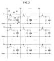
- Fig. 2 is an equivalent circuit diagram illustrating an electric configuration of pixels of the electrophoretic display device according to the first embodiment.
- Fig. 3 is a partial sectional view illustrating a display unit of the electrophoretic display device according to the first embodiment.
- Fig. 4 is a schematic diagram illustrating the configuration of a micro capsule.
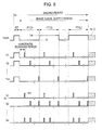
- Fig. 5 is a timing chart illustrating a method of driving the electrophoretic display device according to the first embodiment.
- Fig. 6 is a timing chart illustrating the method of driving the electrophoretic display device according to the first embodiment.
- Figs. 7A to 7D are schematic diagrams illustrating the states of electrophoretic particles when the electrophoretic display device is driven according to the first embodiment.
- Fig. 8 is timing chart illustrating a modified example of Fig. 5 .
- Fig. 9 is a perspective view illustrating the configuration of an electronic paper which is an example of an electronic apparatus using the electrophoretic display device.
- Fig. 10 is a perspective view illustrating the configuration of an electronic book which is an example of the electronic apparatus using the electrophoretic display device.
- An electrophoretic display device will be described with reference to Figs. 1 to Fig. 6 and Figs. 7A to 7D according to a first embodiment.
- Fig. 1 is a block diagram illustrating the overall configuration of the electrophoretic display device according to this embodiment.
- an electrophoretic display device 1 includes a display unit 3, a controller 10, a scanning line driving circuit 60, a data line driving circuit 70, and a common potential supply circuit 220.
- pixels 20 arranged in m rows by n columns are formed in a matrix shape (two-dimensional surface).
- m scanning lines 40 that is, scanning lines Y1, Y2, ..., and Ym
- n data lines 50 that is, data lines X1, X2, ..., and Xn
- the m scanning lines 40 extend in a row direction (that is, an X direction)
- the n data lines 50 extend in a column direction (that is, a Y direction).
- the pixels 20 are disposed in correspondence to locations where the m scanning lines 40 and the n data lines 50 intersect each other.
- the controller 10 controls operations of the scanning line driving circuit 60, the data line driving circuit 70, and the common potential supply circuit 220.
- the controller 10 supplies a clock signal and a timing signal such as a start pulse to the circuits.
- the controller 10 may be included in or be an example of "an image signal supply unit” related to the invention in addition to the scanning line driving circuit 60 and the data line driving circuit 70 described below and may constitute "a common potential supply unit” related to the invention in addition to or instead of the common potential supply circuit 220 described below.
- the scanning line driving circuit 60 supplies a pulse scanning signal sequentially to the scanning lines Y1, Y2, ..., and Ym on the timing signal supplied from the controller 10.
- the data line driving circuit 70 supplies an image signal to the data lines X1, X2, ..., and Xn on the basis of the timing signal supplied from the controller 10.
- the image signal takes a binary potential of a high potential VH (for example, 15 V) or a low potential VL (for example, 0 V).
- VH for example, 15 V
- VL for example, 0 V
- the image signal having the low potential VL is supplied to the pixels 20 to be displayed with a black color and the image signal having the high potential VH is supplied to the pixels 20 to be displayed with a white color.
- the scanning line driving circuit 60 supplies the high potential VH to all the m scanning lines 40 and the data line driving circuit 70 supplies the low potential VL to all the n data lines 50, as described below.
- the common potential supply circuit 220 supplies a common potential Vcom to common potential lines 93.
- Fig. 2 is an equivalent circuit diagram illustrating an electric configuration of the pixels.
- each of the pixels 20 includes a pixel switching transistor 24, a pixel electrode 21, a common electrode 22, an electrophoretic element 23, and a retention capacitor 27.
- the pixel switching transistor 24 is formed of an N-type transistor, for example.
- a gate is electrically connected to the scanning line 40, a source is electrically connected to the data line 50, and a drain is electrically connected to the pixel electrode 21 and the retention capacitor 27.
- the pixel switching transistor 24 outputs the image signal supplied from the data line driving circuit 70 (see Fig. 1 ) through the data line 50 to the pixel electrode 21 and the retention capacitor 27 at timing according to a pulse scanning signal supplied from the scanning line driving circuit 60 through the scanning line 40 (see Fig. 1 ).
- the image signal is supplied from the data line driving circuit 70 to the pixel electrodes 21 through the data lines 50 and the pixel switching transistors 24.
- the pixel electrodes 21 are disposed opposite the common electrode 22 with the electrophoretic element 23 interposed therebetween.
- the common electrode 22 is electrically connected to the common potential lines 93 to which the common potential Vcom is supplied.
- the electrophoretic element 23 includes a plurality of micro capsules which each contain the electrophoretic particles.
- the retention capacitor 27 is constituted by a pair of electrodes disposed opposite to each other through a dielectric film. One electrode of the retention capacitor 27 is electrically connected to the pixel electrode 21 and the pixel switching transistor 24 and the other electrode thereof is electrically connected to the common potential line 93. The retention capacitor 27 holds the image signal for some time.
- Fig. 3 is a partial sectional view illustrating the display unit of the electrophoretic display device according to this embodiment.
- the display unit 3 has a configuration in which the electrophoretic element 23 is interposed between an element substrate 28 and a counter substrate 29. This embodiment will be described on the assumption that an image is displayed on a side of the counter substrate 29.
- the element substrate 28 is an example of "a first substrate” according to the invention and the counter substrate 29 is an example of "a second substrate” according to the invention.
- the element substrate 28 is formed of glass or plastic, for example. On the element substrate 28, even through not shown, a laminated structure is formed in which the pixel switching transistors 24, the retention capacitors 27, the scanning lines 40, the data lines 50, the common potential lines 93, and the like described above with reference to Fig. 2 are laminated. On upper side of the laminated structure, the plurality of pixel electrodes 21 are arranged in a matrix shape.
- the counter substrate 29 is a transparent substrate formed of glass or plastic, for example.
- the common electrode 22 in a solid state is formed opposite the plurality of pixel electrodes 9a on the plane of the counter substrate 29 opposite the element substrate 28.
- the common electrode 22 is formed of a transparent conductive material such as silver magnesium (MgAg), indium tin oxide (ITO), indium zinc oxide (IZO).
- the electrophoretic element 23 includes the plurality of micro capsules 80 containing the electrophoretic particles.
- the electrophoretic element 23 is fixed between the element substrate 28 and the counter substrate 29 by a binder 30 formed of a resin or the like and an adhesive layer 31.
- a binder 30 formed of a resin or the like and an adhesive layer 31.
- an electrophoretic sheet formed by fixing the electrophoretic element 23 to the counter substrate 29 by the binder 30 in advance is attached to the separately manufactured element substrate 28 provided with the pixel electrodes 21 by the adhesive layer 31.
- the micro capsules 80 are interposed between the pixel electrodes 21 and the common electrode 22. In addition, one or the plurality of micro capsules 80 are disposed within one pixel 20 (in other words, for one pixel electrode 21).
- Fig. 4 is a schematic diagram illustrating the configuration of the micro capsule. The cross section of the micro capsule is schematically shown in Fig. 4 .
- the micro capsule 80 includes a dispersion medium 81, a plurality of white particles 82, and a plurality of black particles 83 within a coat membrane 85.
- the micro capsule 80 has a spherical shape with a particle diameter of about 50 ⁇ m, for example.
- the white particles 82 and the black particles 83 are examples of "electrophoretic particles" of the invention.
- the coat membrane 85 functions as an outer shell of the micro capsule 80 formed of transparent polymer resin such as acryl resin such as polymethyl methacrylate and polyethyl methacrylate, urea resin, gum Arabic, and gelatine.
- transparent polymer resin such as acryl resin such as polymethyl methacrylate and polyethyl methacrylate, urea resin, gum Arabic, and gelatine.
- the dispersion medium 81 is a medium for dispersing the white particles 82 and the black particles 83 in the micro capsule 80 (in the words, the coat membrane 85).
- the dispersion medium 81 include water, alcoholic solvent (such as methanol, ethanol, isopropanol, butanol, octanol, and methyl cellosolve), esters (such as ethyl acetate and butyl acetate), ketones (such as acetone, methylethyl ketone, and methyl isobutyl ketone), aliphatic hydrocarbons (such as pentane, hexane, and octane), alicyclic hydrocarbons (such as cyclohexane and methyl cyclohexane), aromatic hydrocarbons (such as benzene, toluene, and benzenes having a long-chain alkyl group (such as xylene, hexyl benzene
- the white particles 82 are particles (polymer or colloid) formed of white pigments such as titanium dioxide, zinc flower, and antimony trioxide and are charged to, for example, negative polarity.
- the black particles 83 are particles (polymer or colloid) formed of black pigments such as aniline black and carbon black and are charged to, for example, positive polarity.
- the white particles 82 and the black particles 83 move in the dispersion medium 81 thanks to an electric field generated by a potential difference between the pixel electrodes 21 and the common electrode 22.
- a charging control agent including particles of electrolyte, surfactant, metal soap, resin, rubber, oil, varnish, or compound, a dispersion solvent such as titanium coupling agent, aluminum coupling agent, and silane coupling agent, lubricant, and stabilizer may be added to the pigments as needed.
- the black particles 83 are gathered on a side of the display surface within the micro capsules 80 to display a color (that is, a black color) of the black particles 83 on the display surface of the display unit 3.
- Red, green, and blue colors can be displayed by replacing the pigments used for the white particles 82 and the black particles 83 with pigments of the red, green and blue colors, for example.
- pixel electrodes 21 B the pixel electrodes 21 of the pixels 20 to be displayed with the black color
- pixel electrodes 21W the pixel electrodes 21 of the pixels 20 to be displayed with the white color
- Figs. 5 and 6 are timing charts illustrating the method of driving the electrophoretic display device according to this embodiment.
- time-dependent variation in the common potential Vcom, the potentials of the scanning lines Y1, Y2, ..., and Ym, and the potentials of the data lines X1, x2, ..., and Xn in an imaging period is shown (that is, a period in which a new image is prepared or written to the plurality of pixels 20 arranged in the display unit 3).
- Fig. 6 time-dependent variation in the potential of the common electrode 22, the potential of the pixel electrodes 21 B, the potential of the pixel electrodes 21 W in the imaging period is shown.
- FIGS. 7A to 7D are schematic diagrams illustrating the states of the electrophoretic particles upon driving the electrophoretic display device according to this embodiment.
- Fig. 7A shows the state of the electrophoretic particles immediately after a reset period.
- Fig. 7B shows the state of the electrophoretic particles immediately after a first frame period.
- Fig. 7C shows the state of the electrophoretic particles immediately after a second frame period.
- Fig. 7D shows the state of the electrophoretic particles immediately after the imaging period.
- a reset operation of displaying the white color on the display surface of the display unit 3 in a reset period RT before an image signal supply period (which is a period in which the image signal is supplied to the pixels 20) in the imaging period is first performed.
- the scanning line driving circuit 60 (see Fig. 1 ) supplies the high potential VH to all the m scanning lines 40 (that is, the scanning lines Y1, Y2, ..., and Ym) and the data line driving circuit 70 supplies the low potential VL to all the n data lines 50 (that is, the data lines X1, X2, ..., and Xm).
- the low potential VL supplied to the data lines 50 is supplied to the pixel electrodes 21 of the pixels 20 via the pixel switching transistors 24 which are turned ON by the high potential VH supplied through the scanning lines 40.
- the pixel electrodes 21 (all the pixel electrodes 21 B and the pixel electrodes 21 W) of the pixels 20 are maintained in the low potential VL (see Fig. 6 ).
- the common potential supply circuit 220 (see Fig. 1 ) supplies the high potential VH as the common potential Vcom to the common potential lines 93. Accordingly, in the reset period RT, the common electrode 22 is maintained in the high potential VH (see Fig. 6 ).
- the black particles 83 charged to the positive polarity are attracted toward the pixel electrodes 21 in the dispersion medium 81 by the Coulomb force and the white particles 82 charged to the negative polarity are attracted toward the common electrode 22 in the dispersion medium 81 by the Coulomb force.
- the white color is displayed on the display surface of the display unit 3.
- the image signal is supplied to the pixels 20 in the image signal supply period followed after the reset period RT in the imaging period.
- the image signal supply period is set as a period which is L (where L is a natural number of 2 or more) times of the frame period or a vertical scanning period (that is, which is set in advance as a period for supplying the scanning signal sequentially to all the m scanning lines 40).
- the image signal supply period contains a first frame period FT(1), a second frame period FT(2), ..., and an L frame period FT(L) in this order.
- each of the frame periods may be set to be in the range of 10 ms to 400 ms, for example.
- the scanning line driving circuit 60 sequentially supplies the pulse scanning signal to the scanning lines Y1, Y2, ..., and Ym in every horizontal scanning period, and the data line driving circuit 70 supplies the image signal having the high potential VH (for example, 15 V) or the low potential VL (for example, 0 V) to the data lines X1, X2, ..., and Xn at timing according to the scanning signal.
- VH for example, 15 V
- VL for example, 0 V
- the image signal having the high potential VH is supplied to the data lines X1 and Xn and the image signal having the low potential VL is also supplied to the data line X2 (in other words, the data line X2 is constantly maintained in the low potential VL) in the initial horizontal scanning period at timing at which the pulse scanning signal is supplied to the scanning line Y1; the image signal having the high potential VH is supplied to the data lines X2 and Xn and the image signal having the low potential VL is also supplied to the data line X1 in the next horizontal scanning period at timing at which the pulse scanning signal is supplied to the scanning line Y2; and the image signal having the high potential VH is supplied to the data line X2 and the image signal having the low potential VL is also supplied to the data lines X1 and Xn in an m-th horizontal scanning period at timing at which the pulse scanning signal is supplied to the scanning line Ym.
- the image signal having the high potential VH is supplied to the pixel electrodes 21 B of the pixel 20 to be displayed with the black color and the image signal having the low potential VL is also supplied to the pixel electrodes 21W of the pixels 20 to be displayed with the white color.
- the pixel electrodes 21 B are constantly maintained in the high potential VH thanks to the potential held by the retention capacitors 27 until the supply of the next image signal having the high potential VH at least in the second frame period FT(2) described below, when the image signal having the high potential VH is supplied at the timing at which the pulse scanning signal is supplied to the scanning lines 40.
- the common potential supply circuit 220 (see Fig. 1 ) supplies the low potential VL as the common potential Vcom to the common potential lines 93 in the first frame period FT(1). Accordingly, in the first frame period FT(1), the common electrode 22 is constantly maintained in the low potential VL (see Fig. 6 ).
- the black particles 83 charged to the positive polarity are attracted toward to the common electrode 22 in the dispersion medium 81 by the Coulomb force and the white particles 82 charged to the negative polarity are attracted toward the pixel electrodes 21 B in the dispersion medium 81 by the Coulomb force between the common electrode 22 constantly maintained in the low potential VL and the pixel electrodes 21 B constantly maintained in the high potential VH.
- the white particles 82 nor the black particles 83 are acted by the Coulomb force, since there is no potential difference between the common electrode 22 constantly maintained in the low potential VL and the pixel electrodes 21 W constantly maintained in the high potential VL.
- the scanning line driving circuit 60 sequentially supplies the pulse scanning signal to the scanning lines Y1, Y2, ..., and Ym in every horizontal scanning period, and the data line driving circuit 70 supplies the image signal having the high potential VH or the low potential VL to the data lines X1, X2, ..., and Xn at timing according to the scanning signal.
- the data line driving circuit 70 supplies the image signal associated with an image to be equally displayed in each of the first frame period FT(1), the second frame period FT(2), ..., and the L frame period FT(L) in the image signal supply period.
- the same image signal as the image signal in the first frame period FT(1) is supplied. That is, in the second frame period FT(2), the same image signal as the image signal in the first frame period FT(1) is written to the pixel electrodes 21 and the retention capacitors 27.
- the pixel electrodes 21 B are constantly maintained in the high potential VH and the pixel electrodes 21 W are constantly maintained in the low potential VL.
- the image signal associated with the image to be equally displayed is supplied to the pixel electrodes 21 in each of the first frame period FT(1), the second frame period FT(2), ..., and the L frame period FT(L)
- the pixel electrodes 21 B are constantly maintained in the high potential VH and the pixel electrodes 21 W are constantly maintained in the low potential VL even in the third frame period FT(3), ..., and the L frame period FT(L).
- the common potential supply circuit 220 (see Fig. 1 ) supplies the high potential VH as the common potential Vcom to the common potential lines 93 in the second frame period FT(2). Accordingly, the common electrode 22 is constantly maintained in the high potential VH in the second frame period FT(2) (see Fig. 6 ).
- the white particles 82 charged to the negative polarity are attracted toward the common electrode 22 in the dispersion medium 81 by the Coulomb force and the black particles 83 charged to the positive polarity are attracted toward the pixel electrodes 21 W in the dispersion medium 81 by the Coulomb force.
- the driving in the first frame period FT(1) is also performed in the third frame period FT(3) followed after the second frame period FT(2). Accordingly, like the driving in the first frame period FT(1) described with reference to Fig. 7B , in the third frame period FT(3), between the common electrode 22 constantly maintained in the low potential VL and the pixel electrodes 21 B constantly maintained in the high potential VH, the black particles 83 charged to the positive polarity are attracted toward the common electrode 22 by the Coulomb force and the white particles 82 charged to the negative polarity are attracted toward to the pixel electrodes 21 B by the Coulomb force. On the other hand, neither the white particles 82 nor the black particles 83 are acted by the Coulomb force between the common electrode 22 constantly maintained in the low potential VL and the pixel electrodes 21 W constantly maintained in the low potential VL.
- the driving in the first frame period FT(1) is performed in the fifth frame period FT(5), the seventh frame period FT(7), etc. (that is, odd-numbered frame periods from an initial odd frame period in the image signal supply period).
- the driving in the second frame period FT(2) is also performed in the fourth frame period FT(4) followed after the third frame period FT(3). Accordingly, like the driving in the second frame period FT(2) described above with reference to Fig. 7C , in the fourth frame period FT(4), neither the white particles 82 nor the black particles 83 are acted by the Coulomb force between the common electrode 22 constantly maintained in the high potential VH and the pixel electrodes 21 B constantly maintained in the high potential VH.
- the white particles 82 charged to the negative polarity are attracted toward the common electrode 22 by the Coulomb force and the black particles 83 charged to the positive polarity are attracted toward the pixel electrodes 21 W by the Coulomb force.
- the driving in the second frame period FT(2) is also performed in the sixth frame period FT(6), the eighth frame period FT(8), etc. (even-numbered frame periods from an initial even frame period in the image signal supply period).
- the voltage according to the image signal is repeatedly applied in an alternate manner between the common electrode 22 and the pixel electrodes 21 B and between the common electrode 22 and the pixel electrodes 21 W. That is, in the odd-numbered frame periods such as the first frame period FT(1) and the third frame period FT(3), the voltage is applied between the common electrode 22 constantly maintained in the low potential VL and the pixel electrodes 21 B constantly maintained in the high potential VH, and no voltage is applied between the common electrode 22 constantly maintained in the low potential VL and the pixel electrodes 21 W constantly maintained in the low potential VL.
- the white particles 82 and the black particles 83 are surely moved between the common electrode 22 and the pixel electrodes 21. That is, it is possible to surely move one of each white particle 82 charged to the negative polarity and each black particle 83 charged to the positive polarity toward the pixel electrode 21 in the dispersion medium 81 and surely move the other thereof toward the common electrode 22 in the dispersion medium 81.
- the voltage according to the same image signal is applied repeatedly several times between the common electrode 22 and the pixel electrodes 21 in a unit of the frame period in the image signal supply period. Therefore, it is possible to surely attract the white particles 82 and the black particles 83 toward the common electrode 22 and the pixel electrodes 21 while preventing the white particles 82 and the black particles 83 from sinking and rising due to the convection currents of the dispersion medium 81 and the gravity action. That is, the voltage according to the same image signal is repeatedly applied between the common electrode 22 and the pixel electrodes 21 B in the odd-numbered frame periods (the first frame period FT(1), the third frame period FT(3), etc.) in the image signal supply period (see Fig. 7B ).
- the voltage according to the same image signal is repeatedly applied between the common electrode 22 and the pixel electrodes 21 W in the even-numbered frame periods (the second frame period FT(2), the fourth frame period FT(4), etc.) in the image signal supply period (see Fig. 7C ). Accordingly, it is possible to surely attract the white particles 82 and the black particles 83 toward the common electrode 22 and the pixel electrodes 21 when the image signal supply period ends (that is, immediately after the L frame period), as shown in Fig. 7D .
- the voltage according to the same image signal is applied repeatedly several times between the common electrode 22 and the pixel electrodes 21 in a unit of the frame period in the image signal supply period, even when a period holding the image signal is relatively shorter in the pixel electrodes 21 and the retention capacitors 28 due to a relatively small capacitance value of the retention capacitors 28. Accordingly, it is possible to surely attract the white particles 82 and the black particles 83 toward the common electrode 22 and the pixel electrodes 21.
- the electrophoretic display device 1 described in this embodiment it is possible to display a high-quality clear image while reducing irregularity in color or brightness between pixels.
- the common electrode 22 and the pixel electrodes 21 (in addition to the common potential lines 93, the scanning lines 40, and the data lines 50) become a high-impedance state (Hi-Z), that is, an electrically disconnected state. In this way, it is possible to prevent leak current between the pixel electrodes 21 adjacent to each other from occurring. Moreover, by suppressing power consumption, it is possible to surely hold the image signal in each of the pixels.
- Hi-Z high-impedance state
- the reset period RT is provided, but the reset period RT need not be provided.
- Fig. 8 is a timing chart illustrating a modified example of the driving method in Fig. 5 .
- the common potential Vcom is switched into a high potential Va lower by a potential difference ⁇ V than the high potential VH of the image signal and a low potential Vb higher by a potential difference ⁇ V than the low potential VL of the image signal, and the high potential Va and the low potential Vb are supplied to the common electrode 22.
- the high potential VH and the low potential VL are 15 V and 0 V, respectively
- the high voltage Va and the low potential Vb are set to 14.5 V and 0.5 V (that is, the differential ⁇ V is set to 0.5 V).
- the potential of 0.5 V is added to the common electrode 22. Therefore, even when the potential of the retention capacitors 28 is lowered, the white particles 82 charged to the negative polarity can be held at the common electrode 22 thanks to the fact that the potential of the common electrode 22 is higher by 0.5 V than the pixel electrodes 21 W which is in the low potential VL. Accordingly, it is possible to prevent the white particles 82 and the black particles 83 from migrating toward an opposite side (moving backward).
- the potential of the common electrode 22 is lowered by 0.5 V from the high potential VH. Therefore, even when the potential of the retention capacitors 28 is lowered, the black particles 83 charged to the positive polarity can be held at the common electrode 22 thanks to the fact that the potential of the common electrode 22 is lower by 0.5 V than that of the pixel electrodes 21 B which is in the high potential VH. Accordingly, it is possible to prevent the white particles 82 and the black particles 83 from moving backward.
- Fig. 9 is a perspective view illustrating the configuration of an electronic paper 1400.
- the electronic paper 1400 includes the electrophoretic display device according to the above-described embodiment as a display unit 1401.
- the electronic paper 1400 has a flexible property and includes a main body 1402 formed of a rewritable sheet having texture like paper and flexibility.
- Fig. 10 is a perspective view illustrating the configuration of an electronic note 1500.
- the electronic note 1500 has a configuration in which plural sheets of electronic papers 1400 shown in Fig. 10 are bound and inserted into a cover 1501.
- the cover 1501 includes a display data input unit (not shown) for inputting display data supplied from an external device. Accordingly, the display details can be changed or updated on the basis of the display data with the bound electronic paper.
- the electronic paper 1400 and the electronic note 1500 described above include the electrophoretic display device according to the above-described embodiment, it is possible to realize low power consumption and a high quality image display.
- the electrophoretic display device can be applied to a display unit of an electronic apparatus such as a wrist watch, a cellular phone, or a portable audio apparatus in addition to the electronic paper and the electronic note.
- an electronic apparatus such as a wrist watch, a cellular phone, or a portable audio apparatus in addition to the electronic paper and the electronic note.
- a modified electrophoretic display device a method of driving the modified electrophoretic display device, and an electronic apparatus including the modified electrophoretic display device are included in the technical scope of the invention.
Landscapes
- Engineering & Computer Science (AREA)
- Physics & Mathematics (AREA)
- Computer Hardware Design (AREA)
- General Physics & Mathematics (AREA)
- Theoretical Computer Science (AREA)
- Electrochromic Elements, Electrophoresis, Or Variable Reflection Or Absorption Elements (AREA)
- Control Of Indicators Other Than Cathode Ray Tubes (AREA)
Abstract
Description
- The present invention relates to an electrophoretic display device, a method of driving the same, and an electronic apparatus.
- An electrophoretic display device is capable of displaying an image by generating a potential difference between pixel electrodes and a common electrode provided in a pair of substrates interposing an electrophoretic element including a dispersion medium containing electrophoretic particles and by moving the electrophoretic particles (for example, see
JP-A-2002-116733 JP-A-2003-140199 JP-A-2004-004714 JP-A-2004-101746 JP-A-2002-116733 JP-A-2004-004714 JP-A-2004-101746 - However, not all the electrophoretic particles behave in completely the same manner, even when a predetermined potential difference is generated between the pixel electrodes and the common electrode in a predetermined period such as one frame period or one horizontal scanning period. Therefore, a problem occurs in that the electrophoretic particles cannot be moved up to a desired location. Moreover, a problem occurs in that the electrophoretic particles may sink or rise due to convection currents of the dispersion medium or gravity action even once the electrophoretic particles are moved to or reach the desired location. Therefore, an image to be displayed is not clear, a residual image occurs, or irregularity in colors or brightness between pixels occurs. That is, a technical problem occurs in that defects with a display may occur.
- An advantage of some aspects of the invention is that it provides an electrophoretic display device capable of displaying a high-quality image, a method of driving the electrophoretic display device, and an electronic apparatus equipped with the electrophoretic display device.
- According to an aspect of the invention, there is provided an electrophoretic display device including: a pair of first and second substrates; an electrophoretic element which is interposed between the first and second substrates and includes a dispersion medium containing electrophoretic particles; a plurality of pixel electrodes which are formed on the first substrate; a common electrode which is formed opposite the plurality of pixel electrodes on the second substrate; an image signal supply unit which supplies an image signal having a first potential or a second potential lower than the first potential to the plurality of pixel electrodes in accordance with image data; and a common potential supply unit which supplies a common potential to the common electrode. The image signal supply unit supplies the image signal to the plurality of pixel electrodes in each of a predetermined number of frame periods in an image signal supply period containing the predetermined number of frame periods in accordance with the image data associated with the same frame image as the image data. In addition, the common potential supply unit switches the common potential into a third potential equal to or lower than the first potential and higher than the second potential and a fourth potential lower than the third potential and equal to or higher than the second potential, and supplies the switched potentials to the common electrode in each of the frame periods in the image signal supply period.
- In the electrophoretic display device according to the aspect of the invention, one pair of the first substrate and the second substrate are disposed so as to be opposed to each other with the electrophoretic element interposed therebetween. On a side of the first substrate opposed to the second substrate, the plurality of pixel electrodes are arranged in a matrix shape in correspondence to intersections of the data lines and the scanning lines which intersect each other on the first substrate, for example. On the first substrate, for example, the transistors as the pixel switching elements, which are provided in the pixels provided with the plurality of pixel electrodes, are capable of performing active matrix driving. On the other hand, on a side of the second substrate opposed to the first substrate, the common electrode is provided in a solid state, for example, so as to be opposed to the plurality of pixel electrodes. The electrophoretic element includes the dispersion medium containing the electrophoretic particles (for example, a plurality of white particles charged to a negative polarity and a plurality of black particles charged to a positive polarity).
- In operation of the electrophoretic display device according to the aspect of the invention, an image is displayed on the display unit including the plurality of pixels by applying voltage (that is, a potential difference) according to the image signal to the electrophoretic element interposed between the pixel electrodes and the common electrode. More specifically, on the basis of the voltage applied between the pixel electrodes and the common electrode, one of each white particle charged to the negative polarity and each black particle charged to the positive polarity is moved (that is, migrated) toward the pixel electrode in the dispersion medium and the other thereof is moved toward the common electrode in the dispersion medium. In this way, an image is displayed on a side of the second substrate in which the common electrode is formed. At this time, the image signal supply unit supplies the image signal having the first potential or the second potential lower than the first potential in accordance with image data to the pixel electrodes through the transistors as the pixel switching elements selected (that is, turned ON) upon supplying the scanning signal through the data lines and the scanning lines. On the other hand, the common potential supply unit supplies the common potential to the common electrode.
- In particular, the image signal supply unit supplies the image signal to the plurality of pixel electrodes in accordance with the image data associated with the same frame image as the image data in each of the predetermined number of frame periods in the image signal supply period containing the predetermined number of frame periods. Moreover, the common potential supply unit switches the common potential into the third potential and the fourth potential lower than the third potential in each of the frame periods in the image signal supply period and supplies the switched potentials to the common electrode. Here, "the image signal supply period" refers to a period in which the image signal according to the image data associated with a frame image, which is an image for one screen to be displayed, is supplied to the pixel electrodes. For example, the image signal supply period is set as a period of ten times of the frame period. "The frame period" is a unit period in which the frame image is displayed and a vertical scanning period (also referred to as one vertical period or one V period) which is set in advance in order to select all the plurality of scanning lines in a predetermined order, for example. The third potential is generally the same potential as the first potential and the fourth potential is generally the same potential as the second potential.
- In a first frame period in the image signal supply period containing the first frame period, a second frame period, ..., and an n-th frame period (where n is a natural number) in this order, the fourth potential (which is generally the same potential as the second potential) as the common potential is supplied to the common electrode. In addition, voltage is applied between the common electrode and the pixel electrodes to which the image signal having the first potential is supplied, and voltage is not applied between the common electrode and the pixel electrodes to which the image signal having the second potential is supplied. In the second frame period followed after the first frame period, the third potential (which is generally the same potential as the first potential) as the common potential is supplied to the common electrode. In addition, no voltage is applied between the common electrode and the pixel electrodes to which the image signal having the first potential is supplied, and voltage is applied between the common electrode and the pixel electrodes to which the image signal having the second potential is supplied. In the third frame period followed after the second frame period, like the first frame period, the fourth potential as the common potential is supplied to the common electrode. In addition, voltage is applied between the common electrode and the pixel electrodes to which the image signal having the first potential is supplied, and no voltage is applied between the common electrode and the pixel electrodes to which the image signal having the second potential is supplied. In the fourth frame period followed after the third frame period, like the second frame period, voltage is applied or not applied between the common electrode and the pixel electrodes. In this way, in the odd-numbered frame period, the fourth potential as the common potential is supplied to the common electrode. In addition, voltage is applied between the common electrode and the pixel electrodes to which the image signal having the first potential is supplied, and no voltage is applied between the common electrode and the pixel electrodes to which the image signal having the second potential is supplied. On the other hand, in the even-numbered frame period, the third potential as the common potential is supplied to the common electrode. In addition, no voltage is applied between the common electrode and the pixel electrodes to which the image signal having the first potential is supplied, and voltage is applied between the common electrode and the pixel electrodes to which the image signal having the second potential is supplied.
- That is, in each of the frame periods in the image signal supply period, the voltage according to the image signal is alternatively applied between the common electrode and the pixel electrodes to which the image signal having the second potential is supplied and between the common electrode and the pixel electrodes to which the image signal having the first potential is supplied.
- Accordingly, it is possible to surely move the electrophoretic particles between the common electrode and the pixel electrodes. That is, one of each white particle charged to the negative polarity and each black particle charged to the positive polarity is surely moved toward the pixel electrode in the dispersion medium and the other thereof is surely moved toward to the common electrode in the dispersion medium.
- In particular, since in the image signal supply period, the voltage according to the image signal corresponding to the image data associated with the same frame image is applied repeatedly several times between the common electrode and the pixel electrodes in a unit of the frame period, it is possible to surely attract the electrophoretic particles toward the common electrode and the pixel electrodes while preventing the electrophoretic particles from sinking and rising due to the convection currents of the dispersion medium and the gravity action. Accordingly, it is possible to improve the contrast of an image to be displayed.
- As a result, in the electrophoretic display device according to the aspect of the invention, it is possible to display a high-quality clear image while reducing a residual image or irregularity in color or brightness between pixels, for example.
- In the electrophoretic display device according to the aspect of the invention, the third potential may be lower than the first potential and the fourth potential may be higher than the second potential.
- According to the aspect of the invention, the electrophoretic particles can be surely moved toward the electrodes to be moved between the pixel electrodes and the common electrode.
- For example, when the first potential and the second potential are set to 15 V and 0 V, respectively, the third potential and the fourth potential may be set to 14.5 V and 0.5 V, respectively. A difference between the first potential and the third potential and a difference between the second potential and the fourth potential may be set as small as possible within ranges in which the first potential is not lower than the third potential and the second potential is not higher than the fourth potential even due to the image signal variation in the common potential.
- The electrophoretic display device according to the aspect of the invention may further include: on the first substrate, data lines and scanning lines which intersect one another; transistors which are formed in correspondence to intersection of the data lines and the scanning lines and electrically connected to the pixel electrodes; and retention capacitors which are electrically connected between the transistors and the pixel electrodes and temporarily hold the image signal. In addition, the image signal supply unit supplies the image signal to the pixel electrodes through the data lines and the scanning lines.
- According to the electrophoretic display device, active matrix driving is possible. Here, the image signal in the pixel electrode is maintained only for some time by the retention capacitors temporarily holding the image signal supplied through the data lines and the transistors. Accordingly, it is possible to further improve the contrast of an image to be displayed.
- According to another aspect of the invention, there is provided a method of driving an electrophoretic display device including a pair of first and second substrates, an electrophoretic element which is interposed between the first and second substrates and includes a dispersion medium containing electrophoretic particles, a plurality of pixel electrodes which are formed on the first substrate, a common electrode which is formed opposite the plurality of pixel electrodes on the second substrate, an image signal supply unit which supplies an image signal having a first potential or a second potential lower than the first potential to the plurality of pixel electrodes in accordance with image data, and a common potential supply unit which supplies a common potential to the common electrode. The method includes: supplying the image signal to the plurality of pixel electrodes in accordance with image data associated with the same frame image as the image data in each of a predetermined number of frame periods in an image signal supply period containing the predetermined number of frame periods by the image signal supply unit; and switching the common potential into a third potential equal to or lower than the first potential and higher than the second potential and a fourth potential lower than the third potential and equal to or higher than the second potential, and supplying the switched potentials to the common electrode in each of the frame periods in the image signal supply period by the common potential supply unit.
- According to the method of driving the electrophoretic display device according to the another aspect of the invention, like the electrophoretic display device described above, it is possible to surely move the electrophoretic particles between the common electrode and the pixel electrodes. Moreover, it is possible to surely attract the electrophoretic particles toward the common electrode and the pixel electrodes while preventing the electrophoretic particles from sinking and rising due to the convection currents of the dispersion medium and the gravity action. As a result, the high-quality image can be displayed.
- Even in the method of driving the electrophoretic display device according to another aspect of the invention, the electrophoretic display device described above according to the aspect of invention can be adopted.
- According to still another aspect of the invention, there is provided an electronic apparatus including the electrophoretic display device having the above-described configuration.
- Since the electronic apparatus includes the electrophoretic display device described above, it is possible to realize various electronic apparatus such as a wrist watch, an electronic paper, an electronic note, a cellular phone, a portable audio apparatus capable of displaying a high-quality image.
- Operations and other advantages of the invention are apparent from exemplary embodiments described below.
- Embodiments of the invention will now be described by way of example only with reference to the accompanying drawings, wherein like numbers reference like elements, and in which:
-
Fig. 1 is a block diagram illustrating an overall configuration of an electrophoretic display device according to a first embodiment. -
Fig. 2 is an equivalent circuit diagram illustrating an electric configuration of pixels of the electrophoretic display device according to the first embodiment. -
Fig. 3 is a partial sectional view illustrating a display unit of the electrophoretic display device according to the first embodiment. -
Fig. 4 is a schematic diagram illustrating the configuration of a micro capsule. -
Fig. 5 is a timing chart illustrating a method of driving the electrophoretic display device according to the first embodiment. -
Fig. 6 is a timing chart illustrating the method of driving the electrophoretic display device according to the first embodiment. -
Figs. 7A to 7D are schematic diagrams illustrating the states of electrophoretic particles when the electrophoretic display device is driven according to the first embodiment. -
Fig. 8 is timing chart illustrating a modified example ofFig. 5 . -
Fig. 9 is a perspective view illustrating the configuration of an electronic paper which is an example of an electronic apparatus using the electrophoretic display device. -
Fig. 10 is a perspective view illustrating the configuration of an electronic book which is an example of the electronic apparatus using the electrophoretic display device. - Hereinafter, preferred embodiments of the invention will be described with reference to the drawings.
- An electrophoretic display device will be described with reference to
Figs. 1 to Fig. 6 andFigs. 7A to 7D according to a first embodiment. - First, an overall configuration of the electrophoretic display device will be described with reference to
Figs. 1 to 2 according to this embodiment. -
Fig. 1 is a block diagram illustrating the overall configuration of the electrophoretic display device according to this embodiment. - According to this embodiment, as shown in
Fig. 1 , anelectrophoretic display device 1 includes adisplay unit 3, acontroller 10, a scanningline driving circuit 60, a dataline driving circuit 70, and a commonpotential supply circuit 220. - In the
display unit 3,pixels 20 arranged in m rows by n columns are formed in a matrix shape (two-dimensional surface). In addition, m scanning lines 40 (that is, scanning lines Y1, Y2, ..., and Ym) and n data lines 50 (that is, data lines X1, X2, ..., and Xn) intersect each other in thedisplay unit 3. Specifically, them scanning lines 40 extend in a row direction (that is, an X direction) and the n data lines 50 extend in a column direction (that is, a Y direction). Thepixels 20 are disposed in correspondence to locations where them scanning lines 40 and the n data lines 50 intersect each other. - The
controller 10 controls operations of the scanningline driving circuit 60, the dataline driving circuit 70, and the commonpotential supply circuit 220. For example, thecontroller 10 supplies a clock signal and a timing signal such as a start pulse to the circuits. In addition, thecontroller 10 may be included in or be an example of "an image signal supply unit" related to the invention in addition to the scanningline driving circuit 60 and the data line drivingcircuit 70 described below and may constitute "a common potential supply unit" related to the invention in addition to or instead of the commonpotential supply circuit 220 described below. - The scanning
line driving circuit 60 supplies a pulse scanning signal sequentially to the scanning lines Y1, Y2, ..., and Ym on the timing signal supplied from thecontroller 10. - The data line driving
circuit 70 supplies an image signal to the data lines X1, X2, ..., and Xn on the basis of the timing signal supplied from thecontroller 10. The image signal takes a binary potential of a high potential VH (for example, 15 V) or a low potential VL (for example, 0 V). In this embodiment, the image signal having the low potential VL is supplied to thepixels 20 to be displayed with a black color and the image signal having the high potential VH is supplied to thepixels 20 to be displayed with a white color. - In this embodiment, in a reset period before an image signal supply period in which the image signal is supplied to the
pixels 20, the scanningline driving circuit 60 supplies the high potential VH to all them scanning lines 40 and the data line drivingcircuit 70 supplies the low potential VL to all the n data lines 50, as described below. - The common
potential supply circuit 220 supplies a common potential Vcom to commonpotential lines 93. - Various signals are input to and output from the
controller 10, the scanningline driving circuit 60, the dataline driving circuit 70, and the commonpotential supply circuit 220, but signals which are not related to this embodiment will not be described. -
Fig. 2 is an equivalent circuit diagram illustrating an electric configuration of the pixels. - In
Fig. 2 , each of thepixels 20 includes apixel switching transistor 24, apixel electrode 21, acommon electrode 22, anelectrophoretic element 23, and aretention capacitor 27. - The
pixel switching transistor 24 is formed of an N-type transistor, for example. In thepixel switching transistor 24, a gate is electrically connected to thescanning line 40, a source is electrically connected to thedata line 50, and a drain is electrically connected to thepixel electrode 21 and theretention capacitor 27. Thepixel switching transistor 24 outputs the image signal supplied from the data line driving circuit 70 (seeFig. 1 ) through thedata line 50 to thepixel electrode 21 and theretention capacitor 27 at timing according to a pulse scanning signal supplied from the scanningline driving circuit 60 through the scanning line 40 (seeFig. 1 ). - The image signal is supplied from the data line driving
circuit 70 to thepixel electrodes 21 through the data lines 50 and thepixel switching transistors 24. Thepixel electrodes 21 are disposed opposite thecommon electrode 22 with theelectrophoretic element 23 interposed therebetween. - The
common electrode 22 is electrically connected to the commonpotential lines 93 to which the common potential Vcom is supplied. - The
electrophoretic element 23 includes a plurality of micro capsules which each contain the electrophoretic particles. - The
retention capacitor 27 is constituted by a pair of electrodes disposed opposite to each other through a dielectric film. One electrode of theretention capacitor 27 is electrically connected to thepixel electrode 21 and thepixel switching transistor 24 and the other electrode thereof is electrically connected to the commonpotential line 93. Theretention capacitor 27 holds the image signal for some time. - Next, a detailed configuration of the display unit of the electrophoretic display device will be described with reference to
Figs. 3 and 4 according to this embodiment. -
Fig. 3 is a partial sectional view illustrating the display unit of the electrophoretic display device according to this embodiment. - In
Fig. 3 , thedisplay unit 3 has a configuration in which theelectrophoretic element 23 is interposed between anelement substrate 28 and acounter substrate 29. This embodiment will be described on the assumption that an image is displayed on a side of thecounter substrate 29. Theelement substrate 28 is an example of "a first substrate" according to the invention and thecounter substrate 29 is an example of "a second substrate" according to the invention. - The
element substrate 28 is formed of glass or plastic, for example. On theelement substrate 28, even through not shown, a laminated structure is formed in which thepixel switching transistors 24, theretention capacitors 27, thescanning lines 40, the data lines 50, the commonpotential lines 93, and the like described above with reference toFig. 2 are laminated. On upper side of the laminated structure, the plurality ofpixel electrodes 21 are arranged in a matrix shape. - The
counter substrate 29 is a transparent substrate formed of glass or plastic, for example. Thecommon electrode 22 in a solid state is formed opposite the plurality of pixel electrodes 9a on the plane of thecounter substrate 29 opposite theelement substrate 28. Thecommon electrode 22 is formed of a transparent conductive material such as silver magnesium (MgAg), indium tin oxide (ITO), indium zinc oxide (IZO). - The
electrophoretic element 23 includes the plurality ofmicro capsules 80 containing the electrophoretic particles. Theelectrophoretic element 23 is fixed between theelement substrate 28 and thecounter substrate 29 by a binder 30 formed of a resin or the like and an adhesive layer 31. In theelectrophoretic display device 1 according to this embodiment, an electrophoretic sheet formed by fixing theelectrophoretic element 23 to thecounter substrate 29 by the binder 30 in advance is attached to the separately manufacturedelement substrate 28 provided with thepixel electrodes 21 by the adhesive layer 31. - The
micro capsules 80 are interposed between thepixel electrodes 21 and thecommon electrode 22. In addition, one or the plurality ofmicro capsules 80 are disposed within one pixel 20 (in other words, for one pixel electrode 21). -
Fig. 4 is a schematic diagram illustrating the configuration of the micro capsule. The cross section of the micro capsule is schematically shown inFig. 4 . - In
Fig. 4 , themicro capsule 80 includes adispersion medium 81, a plurality ofwhite particles 82, and a plurality ofblack particles 83 within acoat membrane 85. Themicro capsule 80 has a spherical shape with a particle diameter of about 50 µm, for example. Thewhite particles 82 and theblack particles 83 are examples of "electrophoretic particles" of the invention. - The
coat membrane 85 functions as an outer shell of themicro capsule 80 formed of transparent polymer resin such as acryl resin such as polymethyl methacrylate and polyethyl methacrylate, urea resin, gum Arabic, and gelatine. - The
dispersion medium 81 is a medium for dispersing thewhite particles 82 and theblack particles 83 in the micro capsule 80 (in the words, the coat membrane 85). Examples of thedispersion medium 81 include water, alcoholic solvent (such as methanol, ethanol, isopropanol, butanol, octanol, and methyl cellosolve), esters (such as ethyl acetate and butyl acetate), ketones (such as acetone, methylethyl ketone, and methyl isobutyl ketone), aliphatic hydrocarbons (such as pentane, hexane, and octane), alicyclic hydrocarbons (such as cyclohexane and methyl cyclohexane), aromatic hydrocarbons (such as benzene, toluene, and benzenes having a long-chain alkyl group (such as xylene, hexyl benzene, heptyl benzene, octyl benzene, nonyl benzene, decyl benzene, undecyl benzene, dodecyl benzene, tridecyl benzene, and tetradecyl benzene)), halogenated hydrocarbon (such as methylene chloride, chloroform, carbon tetrachloride, and 1,2-dichloroethane), carboxylate salt, and other oil substances. These materials may be used singly or as a mixture. Thedispersion medium 81 may be mixed with surfactant. - The
white particles 82 are particles (polymer or colloid) formed of white pigments such as titanium dioxide, zinc flower, and antimony trioxide and are charged to, for example, negative polarity. - The
black particles 83 are particles (polymer or colloid) formed of black pigments such as aniline black and carbon black and are charged to, for example, positive polarity. - Accordingly, the
white particles 82 and theblack particles 83 move in thedispersion medium 81 thanks to an electric field generated by a potential difference between thepixel electrodes 21 and thecommon electrode 22. - A charging control agent including particles of electrolyte, surfactant, metal soap, resin, rubber, oil, varnish, or compound, a dispersion solvent such as titanium coupling agent, aluminum coupling agent, and silane coupling agent, lubricant, and stabilizer may be added to the pigments as needed.
- In
Figs. 3 and 4 , when voltage is applied between thepixel electrodes 21 and thecommon electrode 22 so that the potential of thecommon electrode 22 is relatively higher, theblack particles 83 charged to the positive polarity are attracted toward thepixel electrodes 21 within themicro capsules 80 by the Coulomb force and thewhite particles 82 charged to the negative polarity are attracted toward thecommon electrode 22 within themicro capsules 80 by the Coulomb force. As a result, thewhite particles 82 are gathered on a side of a display surface (that is, a side of the common electrode 22) within themicro capsules 80 to display a color (that is, a white color) of thewhite particles 82 on the display surface of thedisplay unit 3. Conversely, when voltage is applied between thepixel electrodes 21 and thecommon electrode 22 so that the potential of thepixel electrodes 21 is relatively higher, thewhite particles 82 charged to the negative polarity are attracted toward thepixel electrodes 21 by the Coulomb force and theblack particles 83 charged to the positive polarity are attracted toward thecommon electrode 22 by the Coulomb force. As a result, theblack particles 83 are gathered on a side of the display surface within themicro capsules 80 to display a color (that is, a black color) of theblack particles 83 on the display surface of thedisplay unit 3. - Red, green, and blue colors can be displayed by replacing the pigments used for the
white particles 82 and theblack particles 83 with pigments of the red, green and blue colors, for example. - Next, a method of driving the electrophoretic display device according to this embodiment will be described with reference to
Figs. 5 to 7 . Hereinafter, among the plurality ofpixel electrodes 21 arranged in thedisplay unit 3, thepixel electrodes 21 of thepixels 20 to be displayed with the black color are referred to aspixel electrodes 21 B and thepixel electrodes 21 of thepixels 20 to be displayed with the white color are referred to aspixel electrodes 21W. -
Figs. 5 and6 are timing charts illustrating the method of driving the electrophoretic display device according to this embodiment. InFig. 5 , time-dependent variation in the common potential Vcom, the potentials of the scanning lines Y1, Y2, ..., and Ym, and the potentials of the data lines X1, x2, ..., and Xn in an imaging period is shown (that is, a period in which a new image is prepared or written to the plurality ofpixels 20 arranged in the display unit 3). InFig. 6 , time-dependent variation in the potential of thecommon electrode 22, the potential of thepixel electrodes 21 B, the potential of thepixel electrodes 21 W in the imaging period is shown.Figs. 7A to 7D are schematic diagrams illustrating the states of the electrophoretic particles upon driving the electrophoretic display device according to this embodiment.Fig. 7A shows the state of the electrophoretic particles immediately after a reset period.Fig. 7B shows the state of the electrophoretic particles immediately after a first frame period.Fig. 7C shows the state of the electrophoretic particles immediately after a second frame period.Fig. 7D shows the state of the electrophoretic particles immediately after the imaging period. - As shown in
Fig. 5 , a reset operation of displaying the white color on the display surface of thedisplay unit 3 in a reset period RT before an image signal supply period (which is a period in which the image signal is supplied to the pixels 20) in the imaging period is first performed. - That is, as shown in
Figs. 5 and6 , in the reset period RT, the scanning line driving circuit 60 (seeFig. 1 ) supplies the high potential VH to all the m scanning lines 40 (that is, the scanning lines Y1, Y2, ..., and Ym) and the data line drivingcircuit 70 supplies the low potential VL to all the n data lines 50 (that is, the data lines X1, X2, ..., and Xm). In this way, the low potential VL supplied to the data lines 50 is supplied to thepixel electrodes 21 of thepixels 20 via thepixel switching transistors 24 which are turned ON by the high potential VH supplied through the scanning lines 40. Accordingly, in the reset period RT, the pixel electrodes 21 (all thepixel electrodes 21 B and thepixel electrodes 21 W) of thepixels 20 are maintained in the low potential VL (seeFig. 6 ). On the other hand, in the reset period RT, the common potential supply circuit 220 (seeFig. 1 ) supplies the high potential VH as the common potential Vcom to the common potential lines 93. Accordingly, in the reset period RT, thecommon electrode 22 is maintained in the high potential VH (seeFig. 6 ). - As shown in
Fig. 7A , in the reset period RT, theblack particles 83 charged to the positive polarity are attracted toward thepixel electrodes 21 in thedispersion medium 81 by the Coulomb force and thewhite particles 82 charged to the negative polarity are attracted toward thecommon electrode 22 in thedispersion medium 81 by the Coulomb force. As a result, the white color is displayed on the display surface of thedisplay unit 3. - As shown in
Fig. 5 , the image signal is supplied to thepixels 20 in the image signal supply period followed after the reset period RT in the imaging period. In this embodiment, the image signal supply period is set as a period which is L (where L is a natural number of 2 or more) times of the frame period or a vertical scanning period (that is, which is set in advance as a period for supplying the scanning signal sequentially to all the m scanning lines 40). The image signal supply period contains a first frame period FT(1), a second frame period FT(2), ..., and an L frame period FT(L) in this order. In addition, each of the frame periods may be set to be in the range of 10 ms to 400 ms, for example. - Specifically, in the first frame period FT(1) in the image signal supply period, the scanning
line driving circuit 60 sequentially supplies the pulse scanning signal to the scanning lines Y1, Y2, ..., and Ym in every horizontal scanning period, and the data line drivingcircuit 70 supplies the image signal having the high potential VH (for example, 15 V) or the low potential VL (for example, 0 V) to the data lines X1, X2, ..., and Xn at timing according to the scanning signal. In the example shown inFig. 5 , in the first frame period FT(1), the image signal having the high potential VH is supplied to the data lines X1 and Xn and the image signal having the low potential VL is also supplied to the data line X2 (in other words, the data line X2 is constantly maintained in the low potential VL) in the initial horizontal scanning period at timing at which the pulse scanning signal is supplied to the scanning line Y1; the image signal having the high potential VH is supplied to the data lines X2 and Xn and the image signal having the low potential VL is also supplied to the data line X1 in the next horizontal scanning period at timing at which the pulse scanning signal is supplied to the scanning line Y2; and the image signal having the high potential VH is supplied to the data line X2 and the image signal having the low potential VL is also supplied to the data lines X1 and Xn in an m-th horizontal scanning period at timing at which the pulse scanning signal is supplied to the scanning line Ym. That is, in accordance with an image to be displayed, the image signal having the high potential VH is supplied to thepixel electrodes 21 B of thepixel 20 to be displayed with the black color and the image signal having the low potential VL is also supplied to thepixel electrodes 21W of thepixels 20 to be displayed with the white color. - As shown in
Fig. 6 , thepixel electrodes 21 B are constantly maintained in the high potential VH thanks to the potential held by theretention capacitors 27 until the supply of the next image signal having the high potential VH at least in the second frame period FT(2) described below, when the image signal having the high potential VH is supplied at the timing at which the pulse scanning signal is supplied to the scanning lines 40. - On the other hand, as shown in
Figs. 5 and6 , the common potential supply circuit 220 (seeFig. 1 ) supplies the low potential VL as the common potential Vcom to the commonpotential lines 93 in the first frame period FT(1). Accordingly, in the first frame period FT(1), thecommon electrode 22 is constantly maintained in the low potential VL (seeFig. 6 ). - As shown in
Fig. 7B , in the first frame period FT(1), theblack particles 83 charged to the positive polarity are attracted toward to thecommon electrode 22 in thedispersion medium 81 by the Coulomb force and thewhite particles 82 charged to the negative polarity are attracted toward thepixel electrodes 21 B in thedispersion medium 81 by the Coulomb force between thecommon electrode 22 constantly maintained in the low potential VL and thepixel electrodes 21 B constantly maintained in the high potential VH. On the other hand, in the first frame period FT(1) neither thewhite particles 82 nor theblack particles 83 are acted by the Coulomb force, since there is no potential difference between thecommon electrode 22 constantly maintained in the low potential VL and thepixel electrodes 21 W constantly maintained in the high potential VL. - Next, as shown in
Fig. 5 , in the second period FT(2) followed after the first frame period FT(1), the scanningline driving circuit 60 sequentially supplies the pulse scanning signal to the scanning lines Y1, Y2, ..., and Ym in every horizontal scanning period, and the data line drivingcircuit 70 supplies the image signal having the high potential VH or the low potential VL to the data lines X1, X2, ..., and Xn at timing according to the scanning signal. In this embodiment, the dataline driving circuit 70 supplies the image signal associated with an image to be equally displayed in each of the first frame period FT(1), the second frame period FT(2), ..., and the L frame period FT(L) in the image signal supply period. Accordingly, in the second frame period FT(2), the same image signal as the image signal in the first frame period FT(1) is supplied. That is, in the second frame period FT(2), the same image signal as the image signal in the first frame period FT(1) is written to thepixel electrodes 21 and theretention capacitors 27. - As shown in
Fig. 6 , in the second frame period FT(2), thepixel electrodes 21 B are constantly maintained in the high potential VH and thepixel electrodes 21 W are constantly maintained in the low potential VL. In this embodiment, since the image signal associated with the image to be equally displayed is supplied to thepixel electrodes 21 in each of the first frame period FT(1), the second frame period FT(2), ..., and the L frame period FT(L), thepixel electrodes 21 B are constantly maintained in the high potential VH and thepixel electrodes 21 W are constantly maintained in the low potential VL even in the third frame period FT(3), ..., and the L frame period FT(L). - On the other hand, as shown in
Figs. 5 and6 , the common potential supply circuit 220 (seeFig. 1 ) supplies the high potential VH as the common potential Vcom to the commonpotential lines 93 in the second frame period FT(2). Accordingly, thecommon electrode 22 is constantly maintained in the high potential VH in the second frame period FT(2) (seeFig. 6 ). - As shown in
Fig. 7C , in the second frame period FT(2), in thepixel electrodes 21 B neither thewhite particles 82 nor theblack particles 83 are acted by the Coulomb force, since there is no potential difference between thecommon electrode 22 constantly maintained in the high potential VH and thepixel electrodes 21 B constantly maintained in the high potential VH. On the other hand, in the second frame period FT(2), between thecommon electrode 22 constantly maintained in the high potential VH and thepixel electrodes 21 W constantly maintained in the low potential VL, thewhite particles 82 charged to the negative polarity are attracted toward thecommon electrode 22 in thedispersion medium 81 by the Coulomb force and theblack particles 83 charged to the positive polarity are attracted toward thepixel electrodes 21 W in thedispersion medium 81 by the Coulomb force. - In
Figs. 5 and6 , the driving in the first frame period FT(1) is also performed in the third frame period FT(3) followed after the second frame period FT(2). Accordingly, like the driving in the first frame period FT(1) described with reference toFig. 7B , in the third frame period FT(3), between thecommon electrode 22 constantly maintained in the low potential VL and thepixel electrodes 21 B constantly maintained in the high potential VH, theblack particles 83 charged to the positive polarity are attracted toward thecommon electrode 22 by the Coulomb force and thewhite particles 82 charged to the negative polarity are attracted toward to thepixel electrodes 21 B by the Coulomb force. On the other hand, neither thewhite particles 82 nor theblack particles 83 are acted by the Coulomb force between thecommon electrode 22 constantly maintained in the low potential VL and thepixel electrodes 21 W constantly maintained in the low potential VL. - The driving in the first frame period FT(1) is performed in the fifth frame period FT(5), the seventh frame period FT(7), etc. (that is, odd-numbered frame periods from an initial odd frame period in the image signal supply period).
- In
Figs. 5 and6 , the driving in the second frame period FT(2) is also performed in the fourth frame period FT(4) followed after the third frame period FT(3). Accordingly, like the driving in the second frame period FT(2) described above with reference toFig. 7C , in the fourth frame period FT(4), neither thewhite particles 82 nor theblack particles 83 are acted by the Coulomb force between thecommon electrode 22 constantly maintained in the high potential VH and thepixel electrodes 21 B constantly maintained in the high potential VH. On the other hand, between thecommon electrode 22 constantly maintained in the high potential VH and thepixel electrodes 21 W constantly maintained in the low potential VL, thewhite particles 82 charged to the negative polarity are attracted toward thecommon electrode 22 by the Coulomb force and theblack particles 83 charged to the positive polarity are attracted toward thepixel electrodes 21 W by the Coulomb force. - The driving in the second frame period FT(2) is also performed in the sixth frame period FT(6), the eighth frame period FT(8), etc. (even-numbered frame periods from an initial even frame period in the image signal supply period).
- In this way, in the image signal supply period, the voltage according to the image signal is repeatedly applied in an alternate manner between the
common electrode 22 and thepixel electrodes 21 B and between thecommon electrode 22 and thepixel electrodes 21 W. That is, in the odd-numbered frame periods such as the first frame period FT(1) and the third frame period FT(3), the voltage is applied between thecommon electrode 22 constantly maintained in the low potential VL and thepixel electrodes 21 B constantly maintained in the high potential VH, and no voltage is applied between thecommon electrode 22 constantly maintained in the low potential VL and thepixel electrodes 21 W constantly maintained in the low potential VL. On the other hand, in the even-numbered frame periods such as the second frame period FT(2) and the fourth frame period FT(4), no voltage is applied between thecommon electrode 22 constantly maintained in the high potential VH and thepixel electrodes 21 B constantly maintained in the high potential VH, and the voltage is applied between thecommon electrode 22 constantly maintained in the high potential VH and thepixel electrodes 21 W constantly maintained in the low potential VL. - Accordingly, in the image signal supply period, the
white particles 82 and theblack particles 83 are surely moved between thecommon electrode 22 and thepixel electrodes 21. That is, it is possible to surely move one of eachwhite particle 82 charged to the negative polarity and eachblack particle 83 charged to the positive polarity toward thepixel electrode 21 in thedispersion medium 81 and surely move the other thereof toward thecommon electrode 22 in thedispersion medium 81. - In this embodiment, the voltage according to the same image signal is applied repeatedly several times between the
common electrode 22 and thepixel electrodes 21 in a unit of the frame period in the image signal supply period. Therefore, it is possible to surely attract thewhite particles 82 and theblack particles 83 toward thecommon electrode 22 and thepixel electrodes 21 while preventing thewhite particles 82 and theblack particles 83 from sinking and rising due to the convection currents of thedispersion medium 81 and the gravity action. That is, the voltage according to the same image signal is repeatedly applied between thecommon electrode 22 and thepixel electrodes 21 B in the odd-numbered frame periods (the first frame period FT(1), the third frame period FT(3), etc.) in the image signal supply period (seeFig. 7B ). Moreover, the voltage according to the same image signal is repeatedly applied between thecommon electrode 22 and thepixel electrodes 21 W in the even-numbered frame periods (the second frame period FT(2), the fourth frame period FT(4), etc.) in the image signal supply period (seeFig. 7C ). Accordingly, it is possible to surely attract thewhite particles 82 and theblack particles 83 toward thecommon electrode 22 and thepixel electrodes 21 when the image signal supply period ends (that is, immediately after the L frame period), as shown inFig. 7D . - According to the
electrophoretic display device 1 described in this embodiment, the voltage according to the same image signal is applied repeatedly several times between thecommon electrode 22 and thepixel electrodes 21 in a unit of the frame period in the image signal supply period, even when a period holding the image signal is relatively shorter in thepixel electrodes 21 and theretention capacitors 28 due to a relatively small capacitance value of theretention capacitors 28. Accordingly, it is possible to surely attract thewhite particles 82 and theblack particles 83 toward thecommon electrode 22 and thepixel electrodes 21. - As a result, according to the
electrophoretic display device 1 described in this embodiment, it is possible to display a high-quality clear image while reducing irregularity in color or brightness between pixels. - In
Figs. 5 and6 , after the imaging period, thecommon electrode 22 and the pixel electrodes 21 (in addition to the commonpotential lines 93, thescanning lines 40, and the data lines 50) become a high-impedance state (Hi-Z), that is, an electrically disconnected state. In this way, it is possible to prevent leak current between thepixel electrodes 21 adjacent to each other from occurring. Moreover, by suppressing power consumption, it is possible to surely hold the image signal in each of the pixels. - In this embodiment, the reset period RT is provided, but the reset period RT need not be provided.
-
Fig. 8 is a timing chart illustrating a modified example of the driving method inFig. 5 . - As the modified example, as shown in
Fig. 8 , the common potential Vcom is switched into a high potential Va lower by a potential difference ΔV than the high potential VH of the image signal and a low potential Vb higher by a potential difference ΔV than the low potential VL of the image signal, and the high potential Va and the low potential Vb are supplied to thecommon electrode 22. For example, when the high potential VH and the low potential VL are 15 V and 0 V, respectively, the high voltage Va and the low potential Vb are set to 14.5 V and 0.5 V (that is, the differential ΔV is set to 0.5 V). - Even in this case, it is possible to surely move the
white particles 82 and theblack particles 83 toward thepixel electrodes 21 and thecommon electrode 22. - In the odd-numbered frame periods (the first frame period FT(1), the third frame period FT(3), etc.) in the image signal supply period, the potential of 0.5 V is added to the
common electrode 22. Therefore, even when the potential of theretention capacitors 28 is lowered, thewhite particles 82 charged to the negative polarity can be held at thecommon electrode 22 thanks to the fact that the potential of thecommon electrode 22 is higher by 0.5 V than thepixel electrodes 21 W which is in the low potential VL. Accordingly, it is possible to prevent thewhite particles 82 and theblack particles 83 from migrating toward an opposite side (moving backward). - Likewise, in the even-numbered frame periods (the second frame period FT(2), the fourth frame period FT(4), etc.) in the image signal supply period, the potential of the
common electrode 22 is lowered by 0.5 V from the high potential VH. Therefore, even when the potential of theretention capacitors 28 is lowered, theblack particles 83 charged to the positive polarity can be held at thecommon electrode 22 thanks to the fact that the potential of thecommon electrode 22 is lower by 0.5 V than that of thepixel electrodes 21 B which is in the high potential VH. Accordingly, it is possible to prevent thewhite particles 82 and theblack particles 83 from moving backward. - Next, an electronic apparatus to which the electrophoretic display device described above is applied will be described with reference to
Figs. 9 and 10 . Hereinafter, examples in which the electrophoretic display device is applied to an electronic paper and an electronic note will be described. -
Fig. 9 is a perspective view illustrating the configuration of anelectronic paper 1400. - As shown in
Fig. 9 , theelectronic paper 1400 includes the electrophoretic display device according to the above-described embodiment as adisplay unit 1401. Theelectronic paper 1400 has a flexible property and includes amain body 1402 formed of a rewritable sheet having texture like paper and flexibility. -
Fig. 10 is a perspective view illustrating the configuration of anelectronic note 1500. - As shown in
Fig. 10 , theelectronic note 1500 has a configuration in which plural sheets ofelectronic papers 1400 shown inFig. 10 are bound and inserted into acover 1501. Thecover 1501 includes a display data input unit (not shown) for inputting display data supplied from an external device. Accordingly, the display details can be changed or updated on the basis of the display data with the bound electronic paper. - Since the
electronic paper 1400 and theelectronic note 1500 described above include the electrophoretic display device according to the above-described embodiment, it is possible to realize low power consumption and a high quality image display. - The electrophoretic display device according to the above-described embodiment can be applied to a display unit of an electronic apparatus such as a wrist watch, a cellular phone, or a portable audio apparatus in addition to the electronic paper and the electronic note.
- The invention is not limited to the above-described embodiment, but may be modified in various forms without departing from the scope or idea of the invention understood from the accompanying claims and the entire specification. A modified electrophoretic display device, a method of driving the modified electrophoretic display device, and an electronic apparatus including the modified electrophoretic display device are included in the technical scope of the invention.
Claims (5)
- An electrophoretic display device (1) comprising:a pair of first and second substrates (28, 29);an electrophoretic element (80) which is interposed between the first and second substrates and includes a dispersion medium (81) containing electrophoretic particles (82, 83);a plurality of pixel electrodes (21) which are formed on the first substrate (28);a common electrode (22) which is formed opposite the plurality of pixel electrodes on the second substrate (29);an image signal supply unit (10) which supplies an image signal having a first potential (VH) or a second potential (VL) lower than the first potential to the plurality of pixel electrodes (21) in accordance with image data; anda common potential supply unit (220) which supplies a common potential to the common electrode (22),wherein the image signal supply unit (10) supplies the image signal to the plurality of pixel electrodes in each of a predetermined number of frame periods (FT) in an image signal supply period containing the predetermined number of frame periods in accordance with the image data associated with the same frame image as the image data, andwherein the common potential supply unit switches the common potential into a third potential (VH) equal to or lower than the first potential (VH) and higher than the second potential (VL) and a fourth potential (VL) lower than the third potential (VH) and equal to or higher than the second potential (VL), and supplies the switched potentials to the common electrode in each of the frame periods in the image signal supply period.
- The electrophoretic display device according to Claim 1, wherein the third potential is lower than the first potential and the fourth potential is higher than the second potential.
- The electrophoretic display device according to Claim 1 or claim 2, further comprising: on the first substrate (28),
data lines (50) and scanning lines (40) which intersect one another;
transistors (24) which are formed in correspondence to intersection of the data lines and the scanning lines and electrically connected to the pixel electrodes (21); and
retention capacitors (27) which are electrically connected between the transistors and the pixel electrodes and temporarily hold the image signal,
wherein the image signal supply unit supplies the image signal to the pixel electrodes through the data lines and the scanning lines. - A method of driving an electrophoretic display device (1) including a pair of first and second substrates (28, 29), an electrophoretic element (23) which is interposed between the first and second substrates and includes a dispersion medium (81) containing electrophoretic particles (82, 83), a plurality of pixel electrodes (21) which are formed on the first substrate, a common electrode (22) which is formed opposite the plurality of pixel electrodes on the second substrate, an image signal supply unit (10) which supplies an image signal having a first potential (VH) or a second potential (VL) lower than the first potential to the plurality of pixel electrodes in accordance with image data, and a common potential supply unit (220) which supplies a common potential to the common electrode, the method comprising:supplying the image signal to the plurality of pixel electrodes in accordance with the image data associated with the same frame image as the image data in each of a predetermined number of frame periods (FT) in an image signal supply period containing the predetermined number of frame periods by the image signal supply unit; andswitching the common potential into a third potential equal to or lower than the first potential and higher than the second potential and a fourth potential lower than the third potential and equal to or higher than the second potential, and supplying the switched potentials to the common electrode in each of the frame periods in the image signal supply period by the common potential supply unit.
- An electronic apparatus comprising the electrophoretic display device according to any one of Claims 1 to 3.
Applications Claiming Priority (1)
| Application Number | Priority Date | Filing Date | Title |
|---|---|---|---|
| JP2008014605A JP2009175492A (en) | 2008-01-25 | 2008-01-25 | Electrophoretic display device, driving method thereof, and electronic apparatus |
Publications (2)
| Publication Number | Publication Date |
|---|---|
| EP2083414A2 true EP2083414A2 (en) | 2009-07-29 |
| EP2083414A3 EP2083414A3 (en) | 2010-09-29 |
Family
ID=40602398
Family Applications (1)
| Application Number | Title | Priority Date | Filing Date |
|---|---|---|---|
| EP09150248A Withdrawn EP2083414A3 (en) | 2008-01-25 | 2009-01-08 | Electrophoretic display device, method of driving the same, and electronic apparatus |
Country Status (6)
| Country | Link |
|---|---|
| US (1) | US8576163B2 (en) |
| EP (1) | EP2083414A3 (en) |
| JP (1) | JP2009175492A (en) |
| KR (1) | KR20090082134A (en) |
| CN (1) | CN101493627B (en) |
| TW (1) | TW200949792A (en) |
Families Citing this family (22)
| Publication number | Priority date | Publication date | Assignee | Title |
|---|---|---|---|---|
| US8243013B1 (en) | 2007-05-03 | 2012-08-14 | Sipix Imaging, Inc. | Driving bistable displays |
| US20080303780A1 (en) | 2007-06-07 | 2008-12-11 | Sipix Imaging, Inc. | Driving methods and circuit for bi-stable displays |
| JP2011022497A (en) * | 2009-07-17 | 2011-02-03 | Seiko Epson Corp | Electro-optical apparatus, electronic appliance, and method of driving electro-optical apparatus |
| JP5338622B2 (en) * | 2009-11-04 | 2013-11-13 | セイコーエプソン株式会社 | Electrophoretic display device driving method, electrophoretic display device, and electronic apparatus |
| TWI406223B (en) * | 2009-12-15 | 2013-08-21 | Prime View Int Co Ltd | Driving method for pixels of bistable display |
| US11049463B2 (en) * | 2010-01-15 | 2021-06-29 | E Ink California, Llc | Driving methods with variable frame time |
| KR102031848B1 (en) | 2010-01-20 | 2019-10-14 | 가부시키가이샤 한도오따이 에네루기 켄큐쇼 | Electronic device and electronic system |
| US9224338B2 (en) | 2010-03-08 | 2015-12-29 | E Ink California, Llc | Driving methods for electrophoretic displays |
| CN102214426B (en) * | 2010-04-07 | 2013-11-06 | 元太科技工业股份有限公司 | Pixel driving method of bistable display |
| US8681191B2 (en) * | 2010-07-08 | 2014-03-25 | Sipix Imaging, Inc. | Three dimensional driving scheme for electrophoretic display devices |
| CN101887694B (en) * | 2010-07-09 | 2013-03-13 | 友达光电股份有限公司 | Electrophoretic display and driving method thereof |
| TWI420460B (en) | 2011-05-02 | 2013-12-21 | Au Optronics Corp | Electrophoretic panel and driving method thereof |
| US8520295B2 (en) | 2011-06-28 | 2013-08-27 | Hewlett-Packard Development Company, L.P. | Reflective displays |
| US9612739B2 (en) * | 2012-02-02 | 2017-04-04 | Microsoft Technology Licensing, Llc | Low-latency touch-input device |
| JP6001466B2 (en) * | 2013-01-25 | 2016-10-05 | イー インク コーポレイション | Image display medium drive device, image display device, and drive program |
| TWI550332B (en) | 2013-10-07 | 2016-09-21 | 電子墨水加利福尼亞有限責任公司 | Driving methods for color display device |
| US10726760B2 (en) | 2013-10-07 | 2020-07-28 | E Ink California, Llc | Driving methods to produce a mixed color state for an electrophoretic display |
| US10380931B2 (en) | 2013-10-07 | 2019-08-13 | E Ink California, Llc | Driving methods for color display device |
| TWI541784B (en) * | 2014-02-20 | 2016-07-11 | 龍亭新技股份有限公司 | Electrophoretic display device and driving method thereof |
| KR102815310B1 (en) * | 2020-06-05 | 2025-05-30 | 이 잉크 코포레이션 | Methods for achieving color states of less charged particles in an electrophoretic medium containing at least four types of particles |
| WO2023193136A1 (en) * | 2022-04-06 | 2023-10-12 | Huawei Technologies Co., Ltd. | Electronic paper display and display method |
| CN116453478B (en) * | 2023-06-16 | 2023-10-20 | 惠科股份有限公司 | Display module and display device |
Citations (5)
| Publication number | Priority date | Publication date | Assignee | Title |
|---|---|---|---|---|
| JP2002116733A (en) | 2000-06-22 | 2002-04-19 | Seiko Epson Corp | Method for driving electrophoresis display device, driving circuit therefor and electronic equipment |
| JP2003140199A (en) | 2001-08-20 | 2003-05-14 | Seiko Epson Corp | Electrophoresis apparatus, method for driving electrophoresis apparatus, drive circuit for electrophoresis apparatus, and electronic apparatus |
| JP2004004714A (en) | 2002-04-15 | 2004-01-08 | Seiko Epson Corp | Electrophoresis apparatus, method for manufacturing electrophoresis apparatus, and electronic apparatus |
| JP2004101746A (en) | 2002-09-06 | 2004-04-02 | Seiko Epson Corp | Driving method of electrophoretic display device, electrophoretic display panel, control device, electrophoretic display device, and electronic device |
| GB2444794A (en) * | 2006-12-13 | 2008-06-18 | Lg Philips Lcd Co Ltd | Driving an electrophoresis display using an AC common voltage |
Family Cites Families (15)
| Publication number | Priority date | Publication date | Assignee | Title |
|---|---|---|---|---|
| US6563482B1 (en) * | 1999-07-21 | 2003-05-13 | Semiconductor Energy Laboratory Co., Ltd. | Display device |
| JP4059180B2 (en) * | 2003-09-26 | 2008-03-12 | セイコーエプソン株式会社 | Display driver, electro-optical device, and driving method of electro-optical device |
| US20070002009A1 (en) * | 2003-10-07 | 2007-01-04 | Pasch Nicholas F | Micro-electromechanical display backplane and improvements thereof |
| KR20070006727A (en) * | 2004-02-02 | 2007-01-11 | 코닌클리케 필립스 일렉트로닉스 엔.브이. | Electrophoretic display panel |
| JP4182022B2 (en) * | 2004-04-01 | 2008-11-19 | キヤノン株式会社 | Display device panel and display device |
| JP4378771B2 (en) * | 2004-12-28 | 2009-12-09 | セイコーエプソン株式会社 | Electrophoresis device, electrophoretic device driving method, and electronic apparatus |
| JP4718859B2 (en) * | 2005-02-17 | 2011-07-06 | セイコーエプソン株式会社 | Electrophoresis apparatus, driving method thereof, and electronic apparatus |
| JP4609168B2 (en) * | 2005-02-28 | 2011-01-12 | セイコーエプソン株式会社 | Driving method of electrophoretic display device |
| JP4530167B2 (en) * | 2005-09-22 | 2010-08-25 | セイコーエプソン株式会社 | Electrophoresis device, electronic apparatus, and method for driving electrophoresis device |
| US8069452B2 (en) * | 2005-12-01 | 2011-11-29 | Telefonaktiebolaget L M Ericsson (Publ) | Method and management agent for event notifications correlation |
| JP4556244B2 (en) * | 2006-01-20 | 2010-10-06 | セイコーエプソン株式会社 | Driving apparatus and driving method for electrophoretic display panel |
| JP2007206392A (en) * | 2006-02-02 | 2007-08-16 | Epson Imaging Devices Corp | Electro-optical device, driving method thereof, and electronic equipment |
| JP4631768B2 (en) * | 2006-03-22 | 2011-02-16 | セイコーエプソン株式会社 | Electrophoresis device, electronic apparatus, and method for driving electrophoresis device |
| JP5348363B2 (en) | 2006-04-25 | 2013-11-20 | セイコーエプソン株式会社 | Electrophoretic display device, electrophoretic display device driving method, and electronic apparatus |
| JP4887930B2 (en) * | 2006-06-23 | 2012-02-29 | セイコーエプソン株式会社 | Display device and clock |
-
2008
- 2008-01-25 JP JP2008014605A patent/JP2009175492A/en not_active Withdrawn
- 2008-12-09 US US12/330,599 patent/US8576163B2/en active Active
-
2009
- 2009-01-08 EP EP09150248A patent/EP2083414A3/en not_active Withdrawn
- 2009-01-15 TW TW098101349A patent/TW200949792A/en unknown
- 2009-01-16 CN CN2009100020856A patent/CN101493627B/en active Active
- 2009-01-22 KR KR1020090005488A patent/KR20090082134A/en not_active Withdrawn
Patent Citations (5)
| Publication number | Priority date | Publication date | Assignee | Title |
|---|---|---|---|---|
| JP2002116733A (en) | 2000-06-22 | 2002-04-19 | Seiko Epson Corp | Method for driving electrophoresis display device, driving circuit therefor and electronic equipment |
| JP2003140199A (en) | 2001-08-20 | 2003-05-14 | Seiko Epson Corp | Electrophoresis apparatus, method for driving electrophoresis apparatus, drive circuit for electrophoresis apparatus, and electronic apparatus |
| JP2004004714A (en) | 2002-04-15 | 2004-01-08 | Seiko Epson Corp | Electrophoresis apparatus, method for manufacturing electrophoresis apparatus, and electronic apparatus |
| JP2004101746A (en) | 2002-09-06 | 2004-04-02 | Seiko Epson Corp | Driving method of electrophoretic display device, electrophoretic display panel, control device, electrophoretic display device, and electronic device |
| GB2444794A (en) * | 2006-12-13 | 2008-06-18 | Lg Philips Lcd Co Ltd | Driving an electrophoresis display using an AC common voltage |
Also Published As
| Publication number | Publication date |
|---|---|
| TW200949792A (en) | 2009-12-01 |
| CN101493627A (en) | 2009-07-29 |
| CN101493627B (en) | 2013-04-24 |
| US8576163B2 (en) | 2013-11-05 |
| EP2083414A3 (en) | 2010-09-29 |
| US20090189849A1 (en) | 2009-07-30 |
| KR20090082134A (en) | 2009-07-29 |
| JP2009175492A (en) | 2009-08-06 |
Similar Documents
| Publication | Publication Date | Title |
|---|---|---|
| US8576163B2 (en) | Electrophoretic display device, method of driving the same, and electronic apparatus | |
| EP2105914B1 (en) | Electrophoretic display device | |
| KR101555714B1 (en) | Driving method for driving electrophoretic display apparatus electrophoretic display apparatus and electronic device | |
| JP5320757B2 (en) | Electrophoretic display device driving method, electrophoretic display device, and electronic apparatus | |
| CN102737588B (en) | Control method of electro-optic device, control device of electro-optic device, electro-optic device and electronic equipment | |
| US8890907B2 (en) | Method of controlling electro-optical device, control device for electro-optical device, electro-optical device, and electronic apparatus | |
| US9202417B2 (en) | Driving method of electrophoretic display device, and controller | |
| JP5304556B2 (en) | Electrophoretic display device and driving method thereof | |
| JP2015138096A (en) | Electrophoretic display device, driving method of the same, control circuit, and electronic apparatus | |
| US20110216099A1 (en) | Driving method of electrophoretic display device, and controller | |
| JP2012237955A (en) | Control method of electro-optic device, control device of electro-optic device, electro-optic device and electronic equipment | |
| JP5845614B2 (en) | Electro-optical device control method, electro-optical device control device, electro-optical device, and electronic apparatus | |
| JP5445310B2 (en) | Electrophoretic display device, control circuit, electronic apparatus, and driving method | |
| US9343017B2 (en) | Driving method of electrophoretic display device, and controller | |
| JP2009169365A (en) | Electrophoretic display device, driving method thereof, and electronic apparatus | |
| JP2012237958A (en) | Control method of electro-optic device, control device of electro-optic device, electro-optic device and electronic equipment | |
| US8599127B2 (en) | Electrophoretic display device, driving method thereof, and electronic apparatus | |
| US20090243996A1 (en) | Electrophoretic display device, method of driving the same, and electronic apparatus | |
| US20110115774A1 (en) | Driving method for driving electrophoretic apparatus, electrophoretic display apparatus, electronic device, and controller | |
| JP2012220917A (en) | Control method of electro-optic device, control device of electro-optic device, electro-optic device, and electronic apparatus | |
| KR20090103750A (en) | Electrophoretic display device, method of driving the same, and electronic apparatus | |
| JP2012194341A (en) | Control method of electro-optical device, controller of electro-optical device, electro-optical device and electronic apparatus |
Legal Events
| Date | Code | Title | Description |
|---|---|---|---|
| PUAI | Public reference made under article 153(3) epc to a published international application that has entered the european phase |
Free format text: ORIGINAL CODE: 0009012 |
|
| AK | Designated contracting states |
Kind code of ref document: A2 Designated state(s): AT BE BG CH CY CZ DE DK EE ES FI FR GB GR HR HU IE IS IT LI LT LU LV MC MK MT NL NO PL PT RO SE SI SK TR |
|
| AX | Request for extension of the european patent |
Extension state: AL BA RS |
|
| PUAL | Search report despatched |
Free format text: ORIGINAL CODE: 0009013 |
|
| AK | Designated contracting states |
Kind code of ref document: A3 Designated state(s): AT BE BG CH CY CZ DE DK EE ES FI FR GB GR HR HU IE IS IT LI LT LU LV MC MK MT NL NO PL PT RO SE SI SK TR |
|
| AX | Request for extension of the european patent |
Extension state: AL BA RS |
|
| 17P | Request for examination filed |
Effective date: 20110329 |
|
| AKX | Designation fees paid |
Designated state(s): CH DE FR GB LI |
|
| 17Q | First examination report despatched |
Effective date: 20120718 |
|
| STAA | Information on the status of an ep patent application or granted ep patent |
Free format text: STATUS: THE APPLICATION HAS BEEN WITHDRAWN |
|
| 18W | Application withdrawn |
Effective date: 20130411 |