EP2083329A2 - Method and apparatus for structuring a radiation-sensitive material - Google Patents
Method and apparatus for structuring a radiation-sensitive material Download PDFInfo
- Publication number
- EP2083329A2 EP2083329A2 EP09000644A EP09000644A EP2083329A2 EP 2083329 A2 EP2083329 A2 EP 2083329A2 EP 09000644 A EP09000644 A EP 09000644A EP 09000644 A EP09000644 A EP 09000644A EP 2083329 A2 EP2083329 A2 EP 2083329A2
- Authority
- EP
- European Patent Office
- Prior art keywords
- radiation
- material layer
- sensitive material
- layer
- thickness
- Prior art date
- Legal status (The legal status is an assumption and is not a legal conclusion. Google has not performed a legal analysis and makes no representation as to the accuracy of the status listed.)
- Withdrawn
Links
- 230000005855 radiation Effects 0.000 title claims abstract description 287
- 239000000463 material Substances 0.000 title claims abstract description 267
- 238000000034 method Methods 0.000 title claims abstract description 55
- 239000012530 fluid Substances 0.000 claims description 26
- 238000007654 immersion Methods 0.000 claims description 26
- 230000004075 alteration Effects 0.000 claims description 21
- 238000005286 illumination Methods 0.000 claims description 15
- 238000009826 distribution Methods 0.000 claims description 10
- 238000012822 chemical development Methods 0.000 claims description 7
- 239000004065 semiconductor Substances 0.000 claims description 5
- 238000004519 manufacturing process Methods 0.000 claims description 3
- 229920002120 photoresistant polymer Polymers 0.000 description 10
- 230000005670 electromagnetic radiation Effects 0.000 description 8
- 230000003287 optical effect Effects 0.000 description 7
- VYPSYNLAJGMNEJ-UHFFFAOYSA-N Silicium dioxide Chemical compound O=[Si]=O VYPSYNLAJGMNEJ-UHFFFAOYSA-N 0.000 description 6
- 229910052681 coesite Inorganic materials 0.000 description 3
- 229910052906 cristobalite Inorganic materials 0.000 description 3
- 238000011161 development Methods 0.000 description 3
- 230000000694 effects Effects 0.000 description 3
- 230000005686 electrostatic field Effects 0.000 description 3
- 210000001747 pupil Anatomy 0.000 description 3
- 239000000377 silicon dioxide Substances 0.000 description 3
- 229910052682 stishovite Inorganic materials 0.000 description 3
- 229910052905 tridymite Inorganic materials 0.000 description 3
- XLYOFNOQVPJJNP-UHFFFAOYSA-N water Substances O XLYOFNOQVPJJNP-UHFFFAOYSA-N 0.000 description 3
- 238000010586 diagram Methods 0.000 description 2
- 239000011521 glass Substances 0.000 description 2
- 230000002123 temporal effect Effects 0.000 description 2
- XUIMIQQOPSSXEZ-UHFFFAOYSA-N Silicon Chemical compound [Si] XUIMIQQOPSSXEZ-UHFFFAOYSA-N 0.000 description 1
- 230000006978 adaptation Effects 0.000 description 1
- 239000011248 coating agent Substances 0.000 description 1
- 238000000576 coating method Methods 0.000 description 1
- 239000013078 crystal Substances 0.000 description 1
- 238000003384 imaging method Methods 0.000 description 1
- 230000001678 irradiating effect Effects 0.000 description 1
- 238000001459 lithography Methods 0.000 description 1
- 238000004377 microelectronic Methods 0.000 description 1
- 238000001393 microlithography Methods 0.000 description 1
- 229910052710 silicon Inorganic materials 0.000 description 1
- 239000010703 silicon Substances 0.000 description 1
- 230000003068 static effect Effects 0.000 description 1
Images


Classifications
-
- G—PHYSICS
- G03—PHOTOGRAPHY; CINEMATOGRAPHY; ANALOGOUS TECHNIQUES USING WAVES OTHER THAN OPTICAL WAVES; ELECTROGRAPHY; HOLOGRAPHY
- G03F—PHOTOMECHANICAL PRODUCTION OF TEXTURED OR PATTERNED SURFACES, e.g. FOR PRINTING, FOR PROCESSING OF SEMICONDUCTOR DEVICES; MATERIALS THEREFOR; ORIGINALS THEREFOR; APPARATUS SPECIALLY ADAPTED THEREFOR
- G03F7/00—Photomechanical, e.g. photolithographic, production of textured or patterned surfaces, e.g. printing surfaces; Materials therefor, e.g. comprising photoresists; Apparatus specially adapted therefor
- G03F7/70—Microphotolithographic exposure; Apparatus therefor
- G03F7/70216—Mask projection systems
- G03F7/70283—Mask effects on the imaging process
- G03F7/70291—Addressable masks, e.g. spatial light modulators [SLMs], digital micro-mirror devices [DMDs] or liquid crystal display [LCD] patterning devices
-
- G—PHYSICS
- G02—OPTICS
- G02B—OPTICAL ELEMENTS, SYSTEMS OR APPARATUS
- G02B26/00—Optical devices or arrangements for the control of light using movable or deformable optical elements
- G02B26/08—Optical devices or arrangements for the control of light using movable or deformable optical elements for controlling the direction of light
- G02B26/0816—Optical devices or arrangements for the control of light using movable or deformable optical elements for controlling the direction of light by means of one or more reflecting elements
- G02B26/0833—Optical devices or arrangements for the control of light using movable or deformable optical elements for controlling the direction of light by means of one or more reflecting elements the reflecting element being a micromechanical device, e.g. a MEMS mirror, DMD
- G02B26/085—Optical devices or arrangements for the control of light using movable or deformable optical elements for controlling the direction of light by means of one or more reflecting elements the reflecting element being a micromechanical device, e.g. a MEMS mirror, DMD the reflecting means being moved or deformed by electromagnetic means
-
- G—PHYSICS
- G03—PHOTOGRAPHY; CINEMATOGRAPHY; ANALOGOUS TECHNIQUES USING WAVES OTHER THAN OPTICAL WAVES; ELECTROGRAPHY; HOLOGRAPHY
- G03F—PHOTOMECHANICAL PRODUCTION OF TEXTURED OR PATTERNED SURFACES, e.g. FOR PRINTING, FOR PROCESSING OF SEMICONDUCTOR DEVICES; MATERIALS THEREFOR; ORIGINALS THEREFOR; APPARATUS SPECIALLY ADAPTED THEREFOR
- G03F7/00—Photomechanical, e.g. photolithographic, production of textured or patterned surfaces, e.g. printing surfaces; Materials therefor, e.g. comprising photoresists; Apparatus specially adapted therefor
- G03F7/70—Microphotolithographic exposure; Apparatus therefor
- G03F7/70216—Mask projection systems
- G03F7/70341—Details of immersion lithography aspects, e.g. exposure media or control of immersion liquid supply
-
- G—PHYSICS
- G03—PHOTOGRAPHY; CINEMATOGRAPHY; ANALOGOUS TECHNIQUES USING WAVES OTHER THAN OPTICAL WAVES; ELECTROGRAPHY; HOLOGRAPHY
- G03F—PHOTOMECHANICAL PRODUCTION OF TEXTURED OR PATTERNED SURFACES, e.g. FOR PRINTING, FOR PROCESSING OF SEMICONDUCTOR DEVICES; MATERIALS THEREFOR; ORIGINALS THEREFOR; APPARATUS SPECIALLY ADAPTED THEREFOR
- G03F7/00—Photomechanical, e.g. photolithographic, production of textured or patterned surfaces, e.g. printing surfaces; Materials therefor, e.g. comprising photoresists; Apparatus specially adapted therefor
- G03F7/70—Microphotolithographic exposure; Apparatus therefor
- G03F7/70416—2.5D lithography
Definitions
- the invention relates to a method and to an apparatus for structuring a radiation-sensitive material.
- Photon crystals, interconnection layers of semiconductor components and micromechanical elements are the driving force behind the requirement for three-dimensional structuring of elements in the field of microelectronics.
- lithographic methods wherein the semiconductor elements are generated layer by layer using different masks.
- a photoresist also called resist, is first of all applied here to a carrier and exposed by means of a first lithographic mask. This is followed by a chemical development step with which the illumination pattern generated during the preceding exposure in the photoresist is translated into a physical structure in the photoresist.
- exposed regions are removed from the photoresist or, conversely, exposed regions remain while the unexposed regions surrounding the latter are removed from the photoresist.
- the object is achieved according to the invention with a method of structuring a radiation-sensitive material, the method comprising the following steps: providing a layer of the radiation-sensitive material, the radiation-sensitive material being configured such that upon irradiation of the latter with a radiation intensity exceeding a threshold intensity, a characteristic property of the radiation-sensitive material is changed, providing a dynamic mask which is configured to change its structure dynamically, generating a first radiation pattern by means of the dynamic mask in the radiation-sensitive material layer such that the extension of the first radiation pattern, in which the radiation intensity exceeds the threshold intensity, is maximum 50% of the thickness of the material layer in the thickness direction of the material layer at the individual points of the material layer, and generating a second radiation pattern by means of the dynamic mask in the radiation-sensitive material layer.
- the object is achieved according to the invention with an apparatus for structuring a radiation-sensitive material, the apparatus comprising: a holding device for holding a layer of the radiation-sensitive material which is configured such that upon irradiation of the latter with a radiation intensity exceeding a threshold intensity, a characteristic property of the radiation-sensitive material is changed, a dynamic mask which is configured to change its structure dynamically, and a control device which is configured to control the apparatus such that a first radiation pattern is generated by means of the dynamic mask in the radiation-sensitive material layer, the extension of the first radiation pattern, in which the radiation intensity exceeds the threshold intensity, is maximum 50% of the thickness of the material layer in the thickness direction of the material layer at the individual points of the material layer, and that a second radiation pattern is generated by means of the dynamic mask in the radiation-sensitive material layer.
- a layer of radiation-sensitive material is provided.
- This radiation-sensitive material can e.g. be a so-called resist or photoresist which in one embodiment can have a layer thickness of e.g. 10 ⁇ m.
- the change in the characteristic property can be that the radiation-sensitive material is changed upon exposure such that the latter becomes chemically soluble so that in a subsequent chemical development step, contrary to the non-exposed material, it is removed.
- An example of this is positive resist.
- the radiation-sensitive material can also, like a negative resist for example, be configured conversely so that it is not the sufficiently "exposed" material that is removed in the development step, but only the insufficiently exposed material.
- a first radiation pattern is generated in the radiation-sensitive material layer by means of a dynamic mask.
- the first radiation pattern is substantially a radiation distribution extending two-dimensionally within the material layer, but also has an extension in the thickness direction of the material layer.
- the extension of the radiation pattern in the thickness direction of the material layer is maximum 50 % of the thickness of the material layer at the individual points of the material layer, i.e. at respective surface points of the material layer in the perpendicular projection to the material layer.
- the extension of the radiation pattern is understood as meaning the extension in which the radiation intensity exceeds the threshold intensity of the radiation-sensitive material.
- the radiation pattern has a depth of focus of maximum 50 % of the radiation-sensitive material.
- the mask with which the first radiation pattern is produced is configured as a so-called "dynamic mask". Since this is not a mask in the conventional sense, i.e. not a static mask, the structuring method can also be called a mask-free method.
- the dynamic mask is designed to change its structure dynamically, and can for example be designed as a micromirror array, which is also called a DMD (Digital Micromirror Device).
- the individual radiation patterns can be generated in rapid temporal succession. Furthermore, it is no longer necessary for example to readjust a further mask so that the alignment of the individual radiation patterns in relation to one another can also be implemented with a high degree of precision. Since the extension of the first radiation pattern, in which the radiation intensity exceeds the threshold intensity, is maximum 50%, and therefore 50% or less, of the thickness of the layer in the thickness direction of the material layer at the individual points, it is possible only to expose a specific vertical partial region of the radiation-sensitive material or a partial layer of the latter with the first radiation pattern.
- the radiation-sensitive layer By generating a second radiation pattern another vertical region of the radiation-sensitive layer can be exposed. It is therefore possible to expose the radiation-sensitive layer plane by plane and then effect with the result three-dimensional structuring of the radiation-sensitive material. This means that by exposing different depth layers in the radiation-sensitive material layer with different radiation distributions, it becomes possible to provide the radiation-sensitive layer with a desired structure not just in the two dimensions of its main extension, but also in the direction of its thickness extension. In other words, the radiation-sensitive layer is divided virtually into a number of slices lying on top of one another which are respectively provided separately with their own two-dimensional structuring.
- the dynamic mask is in the form of a micromirror array.
- this type of micromirror array is also called a DMD (Digital Micromirror Device).
- This type of micromirror array can for example comprise 10,000 x 10,000 mirrors which respectively have an area of 8 ⁇ 8 ⁇ m.
- the mirrors can be controlled individually.
- the micromirrors are for example mounted on special pivot pins and are tilted by means of electrostatic fields. The electrostatic fields are generated for example by switch logics which are located behind the micromirrors. By tilting a micromirror the beam reflected by this mirror can be deflected to such an extent that the latter no longer passes through downstream projection optics.
- the illumination of a pixel illuminated by this micromirror can be switched on or off.
- a pixel pattern of 10,000 x 10,000 pixels can be flexibly reconfigured, i.e. the pixel pattern can e.g. be reconfigured from the first radiation pattern into the second radiation pattern.
- the mirrors are reduced by a ratio of 1:267 when imaging onto the radiation-sensitive medium. This produces a pixel size of 30 nm in the focus plane and a field size of 300 ⁇ m x 300 ⁇ m.
- the vertical resolution or resolution in the thickness direction of the material layer can be estimated from a Strehl ratio of 80 %, and this corresponds to a RMS wavefront deviation of 0.071 ⁇ .
- the resolution can be estimated as 0.5 x ⁇ /NA.
- ⁇ is the wavelength of the light used for irradiating the radiation-sensitive material and NA the numerical aperture of projection optics used.
- Horizontal resolutions of for example 80 nm can therefore be achieved. Smaller dot sizes can be achieved by using non-linear resists, special illumination settings and by using resolution-enhancing methods, such as for example phase masks and off-center illumination.
- the radiation patterns are projected by means of projection optics with a numerical aperture of at least 0.9, and in particular of at least 1.2.
- a numerical aperture of at least 0.9, and in particular of at least 1.2 With this type of high numerical aperture a relatively small depth of focus can be achieved in the material layer. This enables structuring of the radiation-sensitive material with high resolution in the thickness direction of the material layer.
- the first radiation pattern in a region of the material layer is focussed onto a first focus plane in relation to the material layer, and the second radiation pattern in the same region is focussed onto a second focus plane in relation to the material layer.
- the second focus plane is advantageously offset in relation to the first focus plane in the thickness direction of the material layer.
- the first radiation pattern is focussed onto a first focus position in relation to the material layer
- the second radiation pattern is focussed onto a second focus position in relation to the material layer.
- the extension of the second radiation pattern, in which the radiation intensity exceeds the threshold intensity is also maximum 50 % of the thickness of the material layer in the thickness direction of the material layer at the individual points of the material layer. This enables the independent structuring of individual layers within the material layer by means of the individual radiation patterns.
- the radiation patterns are respectively generated by an illumination distribution generated by the dynamic mask being projected by means of projection optics onto the material layer, and the material layer being moved obliquely to the focus plane of the projection optics.
- the rotational position of the material layer can basically be adjusted differently in relation to the focus plane.
- the material layer can be aligned parallel to the focus plane or also have other rotational positions while it is moved obliquely to the focus plane.
- a region to be exposed is disposed in temporal succession at different focus positions.
- the angle between the movement direction and the focus plane is 1.9°.
- the material layer is moved along a plane tilted in relation to the focus plane of the projection optics, and is thus aligned parallel to the tilted plane.
- the possibility is therefore offered of exposing points in different depth positions in relation to the material layer at the given time with an individual radiation pattern.
- regions already previously exposed in a first depth layer can be structured in a second depth layer lying over the latter, whereas regions which are disposed in the second depth layer in the course of the moving or the scanning movement of the material layer at a later time can be structured in the first depth layer at the same time.
- the tilt angle between the material layer and the focus plane is 1.9°.
- the material layer after generation of the first radiation pattern the material layer is moved in the thickness direction of the material layer, and the second radiation pattern is then generated.
- the radiation patterns are generated by the respective illumination distribution generated by the dynamic mask being projected onto the material layer by means of projection optics, after generation of the first radiation pattern the material layer being moved along the optical axis of the projection optics and the second radiation pattern then being generated.
- the material layer can also be structured three-dimensionally in a very efficient way. Therefore, a thickness section of the material layer can first of all be exposed with the first radiation pattern, and then a thickness section of the material layer lying directly beneath the exposed section can be exposed by means of the second radiation pattern. The material layer is then advantageously moved laterally to the optical axis to such an extent that a previously unexposed region of the material layer can be exposed with the next exposure step.
- the material layer is moved laterally to the thickness direction of the material layer, in particular along the focus plane of the projection optics, and then once again two radiation patterns are generated which are focussed onto different focus planes in relation to the material layer.
- Parallel, two-dimensional sections are advantageously generated here in the radiation-sensitive material to be structured.
- the radiation patterns are generated by a respective illumination distribution generated by the dynamic mask being projected onto the material layer by means of projection optics, and an aberration, in particular the spherical aberration of the projection optics, being changed between the projections of the two radiation patterns.
- an aberration in particular the spherical aberration of the projection optics, being changed between the projections of the two radiation patterns.
- an immersion fluid is disposed on the radiation-sensitive material, the refraction index of the immersion fluid corresponding to the refraction index of the radiation-sensitive material.
- the immersion fluid fills an intermediate space between the projection optics and the radiation-sensitive material.
- the radiation-sensitive material is in the form of nonlinear resist.
- the nonlinear resist is in the form of 2 photon resist.
- a plate of varying thickness made of translucent material is disposed above the radiation-sensitive material, and an intermediate space between the radiation-sensitive material and the plate is filled with an immersion fluid.
- the plate compensates the aforementioned change in aberrations occurring, in particular spherical aberrations.
- the plate can be in the form of a glass plate, for example.
- the layer of immersion fluid should advantageously have a thickness change of +5100 nm and the glass plate a thickness change of -14700 nm.
- a wavelength ⁇ of 193 nm and a numerical aperture (NA) of 1.2 is taken as a basis for the radiated electromagnetic radiation.
- the refraction index here is 1.7 for the radiation-sensitive material 22, 1.43 for the immersion fluid in the form of water, and 1.56 for the wedge-shaped plate of SiO 2 .
- the plate is wedge-shaped in form, and the respective section of the radiation-sensitive material between the focus plane of the projection optics and the surface of the radiation-sensitive material facing towards the plate is also wedge-shaped in form, the wedge formed by the plate and the wedge formed in the radiation-sensitive material having opposing orientations. With this orientation the aberrations that occur can be compensated particularly well.
- the immersion fluid disposed between the plate and the radiation-sensitive material also fills a wedge-shaped volume, the wedge formed by the immersion fluid having the same orientation as the wedge formed by the respective section of the radiation-sensitive material.
- the surface of the plate facing away from the immersion fluid and the respective focus plane of the radiation patterns are parallel to one another.
- the latent images generated by the two radiation patterns in the radiation-sensitive material are developed at the same time by means of a single chemical development step.
- a single chemical development step Unlike conventional three-dimensional structuring methods with which a first resist layer is first of all applied to a wafer, the layer is then exposed and a chemical development takes place after the exposure step, whereupon a further resist layer is applied, it is possible according to the invention to develop the latent images generated in the individual depth layers of the radiation-sensitive material at the same time.
- the layer of the radiation-sensitive material has a thickness of less than 1 mm. Therefore the thickness of the layer is at no location on the layer larger than 1 mm. According to a further variation of the invention the layer has a thickness of less than 100 ⁇ m, in particular less than 20 ⁇ m. According to an embodiment the layer has a uniform thickness within certain tolerances.
- the ratio between the thickness of the layer of the radiation-sensitive material and the area of the layer is smaller than 0,01 m -1 .
- the area refers to the two-dimensional extension of the layer perpendicular to the thickness direction.
- the ratio between the thickness and the area of the layer is smaller than than 0,001 m -1 .
- the ration between the thickness of the layer and the area exposed by the dynamic mask is smaller than 1 m -1 , in particular smaller than 0,01 m -1 .
- the layer of the radiation sensitive material is arranged on a wafer used in semiconductor manufacturing, in particular a silicon wafer.
- the radiation sensitive material is coated onto the whole surface of the wafer, which can have a diameter of e.g. 200 mm or 300 mm.
- Fig. 1 shows an embodiment 10 of an apparatus according to the invention for structuring a layer 22 of a radiation-sensitive material.
- the radiation-sensitive material layer 22 in the form of a photoresist or so-called resist used in microlithography is applied to the surface of a carrier 24 in the form of a wafer by coating.
- the wafer can have a diameter of e.g. 200mm of 300mm.
- the carrier 24 is held by a holding device 27 in the form of a moving stage or a so-called wafer stage.
- the apparatus 10 has a control device 25 for controlling the exposure sequences, in particular the dynamic mask 16 and the holding device 27.
- the layer 22 of the radiation-sensitive material has a thickness d of e.g. 10 ⁇ m.
- the radiation-sensitive material is configured such that upon irradiation of the latter with a radiation intensity exceeding a threshold intensity in a specific wavelength range a characteristic property of the radiation-sensitive material is changed.
- the characteristic property thus changed is that the radiation-sensitive material 22 is chemically changed in the region in question such that in a subsequent development step the radiation-sensitive material 22 can be dissolved away whereas the radiation-sensitive material irradiated with a radiation intensity below the threshold intensity remains unchanged.
- the radiation-sensitive material 22 can also be designed to act conversely so that only the material irradiated with a radiation intensity above the threshold intensity remains during the development step, whereas the material which has been irradiated with a radiation intensity below the threshold intensity is dissolved out.
- the apparatus 10 initially comprises a light source 12 for generating electromagnetic radiation.
- the wavelength of the electromagnetic beams generated by the light source 12 can be in the visible wavelength range, but also in the UV wavelength range, and for example have a wavelength of 248 nm or 193 nm.
- the electromagnetic radiation 13 generated by the light source 12 is conveyed by illumination optics disposed in the optical path to a dynamic mask 16.
- the dynamic mask 16 is in the form of a micromirror array, also called a DMD (Digital Micromirror Device).
- the micromirror array comprises a field-shaped arrangement of 10,000 x 10,000 individual micromirrors 18 which respectively have a mirror surface of 8 x 8 ⁇ m.
- the micromirrors 18 are mounted on special pivot pins and can be tilted individually.
- the inclination of the micromirrors 18 is caused by electrostatic fields which are generated by switch logics located behind the micromirrors 18.
- An individual micromirror 18 forms an optical switch, and by tilting the micromirror 18 the light beam can be deflected to such an extent that it no longer falls into the recording region of downstream projection optics 20, and so is not imaged into the object plane or focus plane 30 of the projection optics 20.
- Each individual micromirror 18 generates one pixel of a radiation pattern in the focus plane 30. By adjusting the individual micromirrors 18 the assigned pixels can be switched on or off.
- the projection optics 20 generally comprise a plurality of lens elements. For the sake of simplification only the final lens element in front of the wafer is shown in Fig. 1 .
- the projection optics 20 have a high numerical aperture (NA), the numerical aperture being for example 1.2.
- NA numerical aperture
- Disposed between the surface 23 of the radiation-sensitive material 22 and the final element of the projection optics 20 is a so-called immersion fluid 28 which has e.g. water.
- the refraction index of the immersion fluid 28 corresponds to the refraction index of the radiation-sensitive material 22. Therefore, the position of a cross-over surface between the immersion fluid 28 and the radiation-sensitive material 22 does not effect the diffraction limited projection.
- the projection optics 20 are designed to image the illumination pattern generated by the micromirror array with a reduction of 1:267, and this results in a pixel size of 30 nm with a field size of 300 ⁇ m x 300 ⁇ m in the focus plane 30.
- the carrier 24 in the form of a wafer, and so also the radiation-sensitive material layer 22 applied to the wafer, is tilted in relation to the focus plane 30 of the projection optics 20 by a tilt angle of approximately 1.9°.
- the carrier 24 is moved along a movement direction 26 tilted by the same tilt angle in relation to the focus plane 30.
- the radiation-sensitive material layer 22 is therefore moved in the plane in which it extends.
- Fig. 2 shows two different positions (I) and (II) of the radiation-sensitive material layer 22 during the scanning movement along the movement direction 26.
- position (I) shown in the upper region of Fig. 2 a first radiation pattern 38 is generated in the material layer 22.
- the first radiation pattern 38 extends in a region of the material layer 22 to be structured identified by reference number 32.
- the focus plane 30 of the projection optics 20 is located in this region in a lower thickness section of the material layer 22 and is identified as the first focus plane 30a with reference to the material layer 22.
- the extension of the first radiation pattern 38 in which the radiation intensity exceeds the threshold intensity of the radiation-sensitive material 22, which is also called the depth of focus 34, is shown graphically in Fig. 2 .
- this extension or depth of focus 34 is maximum 50 % of the thickness d of the material layer 22.
- the depth of focus 34 can also be smaller by orders of magnitude than the thickness d of the material layer. The result of the depth of focus 34 thus limited is that the material layer 22 is only exposed in a limited thickness section and that in the vertical direction adjacent sections remain unexposed. During the scanning movement along the movement direction 26 the radiation pattern changes little by little depending on pre-specified desired structuring of the region 32 in the vertical direction.
- a position identified by (II) is shown in the lower region of Fig. 2 .
- the region 32 to be structured is already pushed further to the right.
- another region in the image field of the dynamic mask 16 is illuminated.
- the focus plane 30 of the projection optics 20 is located in a second focus plane 30b in relation to the material layer 22.
- a second radiation pattern 40 is generated in the second focus plane 30b by the dynamic mask 16.
- the depth of focus 34 of the second radiation pattern 40 is also maximum 50 % of the thickness of the material layer 22. Therefore, in position (II) a thickness section of the region 32 to be structured lying over the thickness section exposed in position (I) is exposed.
- Fig. 3 shows examples of a first radiation pattern 38 and of a second radiation pattern 40 in the focus plane 30, i.e. in a top view as observed in the direction of the optical axis 21 of the projection optics 20.
- the radiation patterns 38 and 40 are examples of radiation patterns generated in the material layer 22 in position (I) and position (II) according to Fig. 2 , by means of which the three-dimensionally structured material layer 22 shown in Fig. 4 can be produced with individual pyramid-type structures.
- Fig. 3 respectively shows the field 36 on the material layer 22 which can be illuminated by means of the dynamic mask 16.
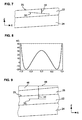
- Fig. 7 shows a further extension of the focus plane 30 in the radiation-sensitive material layer 22 deviating from the extension shown in Fig. 2 upon exposure by means of the apparatus according to Fig. 1 . Since the focus plane 30 extends in the x direction obliquely to the surface 23 of the material layer 22 the effective thickness 44 through which the electromagnetic radiation 13 penetrates upon generation of the radiation pattern changes. This type of change to the effective thickness leads to wavefront aberrations, primarily spherical aberrations.
- Fig. 8 shows as an example the distribution of the wavefront aberrations in mA in the outlet pupil for a resist thickness change of 769 nm.
- Fig. 5 shows a section of a further embodiment of an apparatus 10 for structuring a radiation-sensitive material 22.
- the apparatus 10 according to Fig. 5 only differs from the apparatus 10 according to Fig. 1 in that the carrier 24 with the radiation-sensitive material layer 22 is not scanned obliquely to the focus plane 30 of the projection optics as in Fig. 1 . Instead, the carrier 24 is moved by means of the holding device in the form of a movement stage or wafer stage according to the movement pattern 42 shown in Fig. 5 .
- Fig. 6 shows as an example a first radiation pattern 138 and a second radiation pattern for structuring the object shown in Fig. 4 .
- the structuring method illustrated in the embodiment according to Fig. 5 proceeds as follows: First of all the first radiation pattern 138 is projected into the radiation-sensitive material 22 in a position of the carrier 24 identified by (I). As with the embodiment according to Fig. 1 the depth of focus 34 of the radiation pattern 138 is limited in the thickness direction of the material layer 22 to a fraction of the thickness d. After exposure of the first radiation pattern 138 the material layer 22 is moved downwards along the optical axis 21 of the projection objective 20, i.e. in the z direction according to Fig. 1 .
- a second radiation pattern 140 which is shown as an example in the right-hand region of Fig. 6 , is exposed.
- the second radiation pattern 140 is therefore generated in a different depth layer than the first radiation pattern 138.
- a plurality of radiation patterns are generated along vertical scans in the direction of the z axis.
- the carrier 24 is then moved in the x direction, and a correspondingly formed further radiation pattern is generated in a region of the material layer which has not yet been exposed.
- the carrier 24 is then moved vertically and at least one further exposure is performed.
- the spherical aberration of the projection optics 20 is changed between the projections of the two radiation patterns 138 and 140.
- the projection optics 20 have moveable lens elements which are moved by means of piezo-operated z manipulators.
- Figure 9 shows a further embodiment for compensating the aberrations.
- a plate 46 made of SiO 2 with a wedge-shaped cross-section is disposed above the material layer 22, the intermediate space between the plate 46 and the material layer 22 being filled with immersion fluid 28.
- the surface 48 of the plate 46 facing away from the immersion fluid 28 and the focus plane 30 are parallel to one another.
- the section of the radiation-sensitive material 22 between the focus plane 30 and the surface 23 facing towards the plate 46 is wedge-shaped in form.
- the wedge formed by the plate 46 and the wedge formed by the section of the radiation-sensitive material 22 have orientations opposite one another.
- a change in the effective thickness 44 of the radiation-sensitive material 22 is compensated in the x direction by +10,000 nm with a change in the thickness of the immersion fluid in the z direction by +5,100 nm and at the same time a change in the thickness of the plate 46 nm by -14,700 nm.
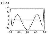
- this compensation for example, the wavefront aberration in the outlet pupil illustrated in Fig. 10 , is produced.
- a wavelength ⁇ of 193 nm and a numerical aperture (NA) of 1.2 is used as a basis here for the radiated electromagnetic radiation.
- the refraction index here is 1.7 for the radiation-sensitive material 22, 1.43 for the immersion fluid in the form of water, and 1.56 for the wedge-shaped plate 46 made of SiO 2 .
- Clause 1 A method of structuring a radiation-sensitive material comprising the steps:
- Clause 2 The method according to clause 1, wherein the dynamic mask is in the form of a micromirror array.
- Clause 3 The method according to clause 1 or 2, wherein the radiation patterns are projected by means of projection optics with a numerical aperture of at least 0.9, and in particular of at least 1.2.
- Clause 4 The method according to any one of the preceding clauses, wherein the first radiation pattern in a region of the material layer is focussed onto a first focus plane in relation to the material layer, and the second radiation pattern in the same region is focussed onto a second focus plane in relation to the material layer.
- Clause 5 The method according to any one of the preceding clauses, wherein the extension of the second radiation pattern, in which the radiation intensity exceeds the threshold intensity, is also maximum 50% of the thickness of the material layer in the thickness direction of the material layer at the individual points of the material layer.
- Clause 6 The method according to any one of the preceding clauses, wherein the radiation patterns are respectively generated by an illumination distribution generated by the dynamic mask being projected by means of projection optics onto the material layer, and the material layer being moved obliquely to the focus plane of the projection optics.
- Clause 7 The method according to the clause 6, wherein the material layer is moved along a plane tilted in relation to the focus plane of the projection optics, and is thus aligned parallel to the tilted plane.
- Clause 8 The method according to any one of the preceding clauses, wherein after generation of the first radiation pattern the material layer is moved in the thickness direction of the material layer, and the second radiation pattern is then generated.
- Clause 9 The method according to clause 8, wherein after generation of the two radiation patterns the material layer is moved laterally to the thickness direction of the material layer, and then once again two radiation patterns are generated which are focussed onto different focus planes in relation to the material layer.
- Clause 10 The method according to any one of the preceding clauses, wherein the radiation patterns are generated by a respective illumination distribution produced by the dynamic mask being projected onto the material layer by means of projection optics, and an aberration of the projection optics being changed between the projections of the two radiation patterns.
- Clause 11 The method according to any one of the preceding clauses, wherein upon generation of the radiation patterns an immersion fluid is disposed on the radiation-sensitive material, the refraction index of the immersion fluid corresponding to the refraction index of the radiation-sensitive material.
- Clause 12 The method according to any one of the preceding clauses, wherein the radiation-sensitive material is in the form of nonlinear resist.
- Clause 13 The method according to any one of the preceding clauses, wherein upon generation of the radiation patterns a plate of varying thickness made of translucent material is disposed above the radiation-sensitive material, and an intermediate space between the radiation-sensitive material and the plate is filled with an immersion fluid.
- Clause 14 The method according to clause 13, wherein the plate is wedge-shaped in form, and the respective section of the radiation-sensitive material between the focus plane of the projection optics and the surface of the radiation-sensitive material facing towards the plate is also wedge-shaped in form, the wedge formed by the plate and the wedge formed in the radiation-sensitive material having opposing orientations.
- Clause 15 The method according to clause 14, wherein the immersion fluid disposed between the plate and the radiation-sensitive material also fills a wedge-shaped volume, the wedge formed by the immersion fluid having the same orientation as the wedge formed by the respective section of the radiation-sensitive material.
- Clause 16 The method according to clause 14 or 15, wherein the surface of the plate facing away from the immersion fluid and the focus plane of the projection optics are parallel to one another.
- Clause 17 The method according to any one of the preceding clauses, wherein the latent images generated by the two radiation patterns in the radiation-sensitive material are developed at the same time by means of a single chemical development step.
- Clause 18 The method according to any one of the preceding clauses, wherein the layer of the radiation-sensitive material has a thickness of less than 1 mm.
- Clause 19 The method according to any one of the preceding clauses, wherein the ratio between the thickness of the layer of the radiation-sensitive material and the area of the layer is smaller than 0,01 m -1 .
- Clause 20 The method according to any one of the preceding clauses, wherein the layer of the radiation sensitive material is arranged on a wafer used in semiconductor manufacturing.
- An apparatus for structuring a radiation-sensitive material comprising:
- Clause 22 The apparatus according to clause 21, which is configured to perform the method according to any one of the clauses 1 to 20.
Landscapes
- Physics & Mathematics (AREA)
- General Physics & Mathematics (AREA)
- Electromagnetism (AREA)
- Optics & Photonics (AREA)
- Exposure And Positioning Against Photoresist Photosensitive Materials (AREA)
- Manufacturing Of Printed Circuit Boards (AREA)
- Manufacturing Of Printed Wiring (AREA)
Abstract
Description
- The invention relates to a method and to an apparatus for structuring a radiation-sensitive material.
- Photon crystals, interconnection layers of semiconductor components and micromechanical elements are the driving force behind the requirement for three-dimensional structuring of elements in the field of microelectronics. Generally, in order to generate three-dimensional structures one uses, for example, lithographic methods wherein the semiconductor elements are generated layer by layer using different masks. A photoresist, also called resist, is first of all applied here to a carrier and exposed by means of a first lithographic mask. This is followed by a chemical development step with which the illumination pattern generated during the preceding exposure in the photoresist is translated into a physical structure in the photoresist. Here either exposed regions are removed from the photoresist or, conversely, exposed regions remain while the unexposed regions surrounding the latter are removed from the photoresist. The result is a two-dimensionally structured photoresist layer. However, in order to achieve three-dimensional structuring the aforementioned steps, namely the application of a photoresist layer, the exposure of the layer and the subsequent chemical development must be repeated a number of times with different lithography masks. However, this method is very complex, and so time-consuming and cost-intensive.
- It is an object of the invention to solve the aforementioned problems, and in particular to improve a method and an apparatus of the type specified at the start such that three-dimensional structuring of a radiation-sensitive material in a more time-efficient and more cost-saving way is made possible.
- The object is achieved according to the invention with a method of structuring a radiation-sensitive material, the method comprising the following steps: providing a layer of the radiation-sensitive material, the radiation-sensitive material being configured such that upon irradiation of the latter with a radiation intensity exceeding a threshold intensity, a characteristic property of the radiation-sensitive material is changed, providing a dynamic mask which is configured to change its structure dynamically, generating a first radiation pattern by means of the dynamic mask in the radiation-sensitive material layer such that the extension of the first radiation pattern, in which the radiation intensity exceeds the threshold intensity, is maximum 50% of the thickness of the material layer in the thickness direction of the material layer at the individual points of the material layer, and generating a second radiation pattern by means of the dynamic mask in the radiation-sensitive material layer.
- Furthermore, the object is achieved according to the invention with an apparatus for structuring a radiation-sensitive material, the apparatus comprising: a holding device for holding a layer of the radiation-sensitive material which is configured such that upon irradiation of the latter with a radiation intensity exceeding a threshold intensity, a characteristic property of the radiation-sensitive material is changed, a dynamic mask which is configured to change its structure dynamically, and a control device which is configured to control the apparatus such that a first radiation pattern is generated by means of the dynamic mask in the radiation-sensitive material layer, the extension of the first radiation pattern, in which the radiation intensity exceeds the threshold intensity, is maximum 50% of the thickness of the material layer in the thickness direction of the material layer at the individual points of the material layer, and that a second radiation pattern is generated by means of the dynamic mask in the radiation-sensitive material layer.
- In other words, according to the invention a layer of radiation-sensitive material is provided. This radiation-sensitive material can e.g. be a so-called resist or photoresist which in one embodiment can have a layer thickness of e.g. 10 µm. Upon irradiation with electromagnetic radiation, for example of a specific wavelength range, upon exceeding a specific radiation intensity the radiation-sensitive material changes a characteristic property. The change in the characteristic property can be that the radiation-sensitive material is changed upon exposure such that the latter becomes chemically soluble so that in a subsequent chemical development step, contrary to the non-exposed material, it is removed. An example of this is positive resist. The radiation-sensitive material can also, like a negative resist for example, be configured conversely so that it is not the sufficiently "exposed" material that is removed in the development step, but only the insufficiently exposed material.
- According to the invention, a first radiation pattern is generated in the radiation-sensitive material layer by means of a dynamic mask. The first radiation pattern is substantially a radiation distribution extending two-dimensionally within the material layer, but also has an extension in the thickness direction of the material layer. The extension of the radiation pattern in the thickness direction of the material layer is maximum 50 % of the thickness of the material layer at the individual points of the material layer, i.e. at respective surface points of the material layer in the perpendicular projection to the material layer. Here the extension of the radiation pattern is understood as meaning the extension in which the radiation intensity exceeds the threshold intensity of the radiation-sensitive material.
- In other words, the radiation pattern has a depth of focus of maximum 50 % of the radiation-sensitive material. The mask with which the first radiation pattern is produced is configured as a so-called "dynamic mask". Since this is not a mask in the conventional sense, i.e. not a static mask, the structuring method can also be called a mask-free method. The dynamic mask is designed to change its structure dynamically, and can for example be designed as a micromirror array, which is also called a DMD (Digital Micromirror Device).
- By making provision for this type of dynamic mask, a number of radiation patterns can be generated one after the other in the radiation-sensitive material without it being necessary to change the mask. Therefore, the individual radiation patterns can be generated in rapid temporal succession. Furthermore, it is no longer necessary for example to readjust a further mask so that the alignment of the individual radiation patterns in relation to one another can also be implemented with a high degree of precision. Since the extension of the first radiation pattern, in which the radiation intensity exceeds the threshold intensity, is maximum 50%, and therefore 50% or less, of the thickness of the layer in the thickness direction of the material layer at the individual points, it is possible only to expose a specific vertical partial region of the radiation-sensitive material or a partial layer of the latter with the first radiation pattern.
- By generating a second radiation pattern another vertical region of the radiation-sensitive layer can be exposed. It is therefore possible to expose the radiation-sensitive layer plane by plane and then effect with the result three-dimensional structuring of the radiation-sensitive material. This means that by exposing different depth layers in the radiation-sensitive material layer with different radiation distributions, it becomes possible to provide the radiation-sensitive layer with a desired structure not just in the two dimensions of its main extension, but also in the direction of its thickness extension. In other words, the radiation-sensitive layer is divided virtually into a number of slices lying on top of one another which are respectively provided separately with their own two-dimensional structuring.
- In one embodiment according to the invention the dynamic mask is in the form of a micromirror array. As already mentioned above, this type of micromirror array is also called a DMD (Digital Micromirror Device). This type of micromirror array can for example comprise 10,000 x 10,000 mirrors which respectively have an area of 8 × 8 µm. The mirrors can be controlled individually. The micromirrors are for example mounted on special pivot pins and are tilted by means of electrostatic fields. The electrostatic fields are generated for example by switch logics which are located behind the micromirrors. By tilting a micromirror the beam reflected by this mirror can be deflected to such an extent that the latter no longer passes through downstream projection optics. In this way, by controlling the micromirror, the illumination of a pixel illuminated by this micromirror can be switched on or off. By means of an array of 10,000 x 10,000 micromirrors a pixel pattern of 10,000 x 10,000 pixels can be flexibly reconfigured, i.e. the pixel pattern can e.g. be reconfigured from the first radiation pattern into the second radiation pattern. In one example, the mirrors are reduced by a ratio of 1:267 when imaging onto the radiation-sensitive medium. This produces a pixel size of 30 nm in the focus plane and a field size of 300 µm x 300 µm. The vertical resolution or resolution in the thickness direction of the material layer can be estimated from a Strehl ratio of 80 %, and this corresponds to a RMS wavefront deviation of 0.071 λ. In a horizontal direction the resolution can be estimated as 0.5 x λ/NA. λ is the wavelength of the light used for irradiating the radiation-sensitive material and NA the numerical aperture of projection optics used. Horizontal resolutions of for example 80 nm can therefore be achieved. Smaller dot sizes can be achieved by using non-linear resists, special illumination settings and by using resolution-enhancing methods, such as for example phase masks and off-center illumination.
- In a further embodiment according to the invention the radiation patterns are projected by means of projection optics with a numerical aperture of at least 0.9, and in particular of at least 1.2. With this type of high numerical aperture a relatively small depth of focus can be achieved in the material layer. This enables structuring of the radiation-sensitive material with high resolution in the thickness direction of the material layer.
- In a further embodiment according to the invention the first radiation pattern in a region of the material layer is focussed onto a first focus plane in relation to the material layer, and the second radiation pattern in the same region is focussed onto a second focus plane in relation to the material layer. The second focus plane is advantageously offset in relation to the first focus plane in the thickness direction of the material layer. In other words, the first radiation pattern is focussed onto a first focus position in relation to the material layer, and the second radiation pattern is focussed onto a second focus position in relation to the material layer.
- In a further embodiment according to the invention the extension of the second radiation pattern, in which the radiation intensity exceeds the threshold intensity, is also maximum 50 % of the thickness of the material layer in the thickness direction of the material layer at the individual points of the material layer. This enables the independent structuring of individual layers within the material layer by means of the individual radiation patterns.
- In a further embodiment according to the invention the radiation patterns are respectively generated by an illumination distribution generated by the dynamic mask being projected by means of projection optics onto the material layer, and the material layer being moved obliquely to the focus plane of the projection optics. Here the rotational position of the material layer can basically be adjusted differently in relation to the focus plane. For example, the material layer can be aligned parallel to the focus plane or also have other rotational positions while it is moved obliquely to the focus plane. By means of the oblique movement of the material layer, a region to be exposed is disposed in temporal succession at different focus positions. If the structure of the mask is now changed dynamically and exposed at appropriate times onto the material layer, a number of radiation patterns can be generated in an efficient and time-saving way at different positions within the thickness extension of the material layer. In one embodiment the angle between the movement direction and the focus plane is 1.9°.
- In a further embodiment according to the invention the material layer is moved along a plane tilted in relation to the focus plane of the projection optics, and is thus aligned parallel to the tilted plane. This means that the material layer is moved in the plane in which it is disposed. The possibility is therefore offered of exposing points in different depth positions in relation to the material layer at the given time with an individual radiation pattern. This enables particularly efficient three-dimensional structuring of the material layer because parallel structuring is thus made possible. At a given time, regions already previously exposed in a first depth layer can be structured in a second depth layer lying over the latter, whereas regions which are disposed in the second depth layer in the course of the moving or the scanning movement of the material layer at a later time can be structured in the first depth layer at the same time. In one embodiment the tilt angle between the material layer and the focus plane is 1.9°.
- In a further embodiment according to the invention, after generation of the first radiation pattern the material layer is moved in the thickness direction of the material layer, and the second radiation pattern is then generated. In particular, the radiation patterns are generated by the respective illumination distribution generated by the dynamic mask being projected onto the material layer by means of projection optics, after generation of the first radiation pattern the material layer being moved along the optical axis of the projection optics and the second radiation pattern then being generated. With this method the material layer can also be structured three-dimensionally in a very efficient way. Therefore, a thickness section of the material layer can first of all be exposed with the first radiation pattern, and then a thickness section of the material layer lying directly beneath the exposed section can be exposed by means of the second radiation pattern. The material layer is then advantageously moved laterally to the optical axis to such an extent that a previously unexposed region of the material layer can be exposed with the next exposure step.
- In a further embodiment according to the invention, after generation of the two radiation patterns the material layer is moved laterally to the thickness direction of the material layer, in particular along the focus plane of the projection optics, and then once again two radiation patterns are generated which are focussed onto different focus planes in relation to the material layer. Parallel, two-dimensional sections are advantageously generated here in the radiation-sensitive material to be structured.
- In a further embodiment according to the invention the radiation patterns are generated by a respective illumination distribution generated by the dynamic mask being projected onto the material layer by means of projection optics, and an aberration, in particular the spherical aberration of the projection optics, being changed between the projections of the two radiation patterns. One thus allows for the fact that upon generation of the individual radiation patterns the electromagnetic radiation must penetrate through material layers of different thicknesses, i.e. the effective thickness of the material layer is different. This leads to aberrations, in particularly dominantly spherical aberrations when generating the individual radiation patterns. According to the present embodiment according to the invention this effect is compensated by dynamic adaptation of the aberration, in particular of the spherical aberration. This manipulation of the spherical aberration can be brought about e.g. by means of moveable lens elements in the projection optics the position of which is changed in particular by means of piezo-operated z manipulations.
- In a further embodiment according to the invention, upon generation of the radiation patterns an immersion fluid is disposed on the radiation-sensitive material, the refraction index of the immersion fluid corresponding to the refraction index of the radiation-sensitive material. In particular, the immersion fluid fills an intermediate space between the projection optics and the radiation-sensitive material. By providing the immersion fluid, the refraction index of which corresponds to the refraction index of the radiation-sensitive material, the diffraction-limited projection is not effected by the cross-over surface between the immersion fluid and the radiation-sensitive material.
- In a further embodiment according to the invention the radiation-sensitive material is in the form of nonlinear resist. Advantageously, the nonlinear resist is in the form of 2 photon resist. These types of resist do not accumulate the exposure dose over a longer period, but show a nonlinear reaction to the instantaneous intensity. It is therefore possible to achieve three-dimensional structuring with the method according to the invention in the dynamic scanning operation with high resolution.
- In a further embodiment, upon generation of the radiation patterns a plate of varying thickness made of translucent material is disposed above the radiation-sensitive material, and an intermediate space between the radiation-sensitive material and the plate is filled with an immersion fluid. The plate compensates the aforementioned change in aberrations occurring, in particular spherical aberrations. The plate can be in the form of a glass plate, for example. With an effective thickness change of the resist between different illumination settings, i.e. the z distance between two different radiation patterns of +10 µm generated in the material layer, the layer of immersion fluid should advantageously have a thickness change of +5100 nm and the glass plate a thickness change of -14700 nm. In this case a wavelength λ of 193 nm and a numerical aperture (NA) of 1.2 is taken as a basis for the radiated electromagnetic radiation. The refraction index here is 1.7 for the radiation-
sensitive material 22, 1.43 for the immersion fluid in the form of water, and 1.56 for the wedge-shaped plate of SiO2. - In a further embodiment according to the invention the plate is wedge-shaped in form, and the respective section of the radiation-sensitive material between the focus plane of the projection optics and the surface of the radiation-sensitive material facing towards the plate is also wedge-shaped in form, the wedge formed by the plate and the wedge formed in the radiation-sensitive material having opposing orientations. With this orientation the aberrations that occur can be compensated particularly well.
- In a further embodiment according to the invention the immersion fluid disposed between the plate and the radiation-sensitive material also fills a wedge-shaped volume, the wedge formed by the immersion fluid having the same orientation as the wedge formed by the respective section of the radiation-sensitive material.
- In a further embodiment according to the invention the surface of the plate facing away from the immersion fluid and the respective focus plane of the radiation patterns are parallel to one another.
- In a further embodiment according to the invention the latent images generated by the two radiation patterns in the radiation-sensitive material are developed at the same time by means of a single chemical development step. Unlike conventional three-dimensional structuring methods with which a first resist layer is first of all applied to a wafer, the layer is then exposed and a chemical development takes place after the exposure step, whereupon a further resist layer is applied, it is possible according to the invention to develop the latent images generated in the individual depth layers of the radiation-sensitive material at the same time.
- According to a further embodiment of the invention the layer of the radiation-sensitive material has a thickness of less than 1 mm. Therefore the thickness of the layer is at no location on the layer larger than 1 mm. According to a further variation of the invention the layer has a thickness of less than 100 µm, in particular less than 20 µm. According to an embodiment the layer has a uniform thickness within certain tolerances.
- According to a further embodiment of the invention the ratio between the thickness of the layer of the radiation-sensitive material and the area of the layer is smaller than 0,01 m-1. The area refers to the two-dimensional extension of the layer perpendicular to the thickness direction. According to a variation the ratio between the thickness and the area of the layer is smaller than than 0,001 m-1. According to a further embodiment of the invention the ration between the thickness of the layer and the area exposed by the dynamic mask is smaller than 1 m-1, in particular smaller than 0,01 m-1.
- According to a further embodiment of the invention the layer of the radiation sensitive material is arranged on a wafer used in semiconductor manufacturing, in particular a silicon wafer. According to a variation of the invention the radiation sensitive material is coated onto the whole surface of the wafer, which can have a diameter of e.g. 200 mm or 300 mm.
- The features specified with regard to the embodiments of the method according to the invention listed above can be applied correspondingly to the apparatus according to the invention. The resulting embodiments of the apparatus according to the invention are to be explicitly included in the disclosure of the invention. Furthermore, the advantages listed above with regard to the embodiments of the method according to the invention therefore also relate to the corresponding embodiments of the apparatus according to the invention.
- In the following exemplary embodiments of a method according to the invention and of an apparatus according to the invention for structuring a radiation-sensitive material are described in greater detail by means of the attached schematic drawings. These show as follows:
-
Fig. 1 an embodiment of an apparatus according to the invention for structuring a radiation-sensitive material, -
Fig. 2 a section of the radiation-sensitive material structured by means of the apparatus according toFig. 1 in two different positions (I) and (II) adopted during an exposure procedure, -
Fig. 3 examples of respective radiation patterns generated in the two positions (I) and (II) according toFig. 2 in the radiation-sensitive material in a top view onto the radiation-sensitive material layer, -
Fig. 4 a perspective view of a material layer structured by means of the radiation pattern shown inFig. 3 , -
Fig. 5 a section of a further embodiment of an apparatus for structuring a radiation-sensitive material according to the invention, -
Fig. 6 examples of respective radiation patterns generated in two different positions (I) and (II) in the radiation-sensitive material in a top view onto the material layer, -
Fig. 7 a sectional view of the radiation-sensitive material during implementation of the method according to the invention in order to illustrate the extension of the focus plane, -
Fig. 8 a diagram to illustrate the wavefront aberration in the outlet pupil when changing the thickness of the radiation-sensitive material by a certain amount, -
Fig. 9 a sectional view of an arrangement according to the invention of different layers over the radiation-sensitive material, -
Fig. 10 a diagram showing the wavefront aberration according toFig. 8 for the arrangement according toFig. 9 . - In the exemplary embodiments described below elements which are similar to one another functionally or structurally are provided as far as possible with the same or similar reference numbers. Therefore, in order to understand the features of the individual elements of a specific exemplary embodiment, reference should be made to the description of other exemplary embodiments or to the general
-
Fig. 1 shows anembodiment 10 of an apparatus according to the invention for structuring alayer 22 of a radiation-sensitive material. The radiation-sensitive material layer 22 in the form of a photoresist or so-called resist used in microlithography is applied to the surface of acarrier 24 in the form of a wafer by coating. The wafer can have a diameter of e.g. 200mm of 300mm. Thecarrier 24 is held by a holdingdevice 27 in the form of a moving stage or a so-called wafer stage. Furthermore, theapparatus 10 has acontrol device 25 for controlling the exposure sequences, in particular thedynamic mask 16 and the holdingdevice 27. - The
layer 22 of the radiation-sensitive material has a thickness d of e.g. 10 µm. The radiation-sensitive material is configured such that upon irradiation of the latter with a radiation intensity exceeding a threshold intensity in a specific wavelength range a characteristic property of the radiation-sensitive material is changed. The characteristic property thus changed is that the radiation-sensitive material 22 is chemically changed in the region in question such that in a subsequent development step the radiation-sensitive material 22 can be dissolved away whereas the radiation-sensitive material irradiated with a radiation intensity below the threshold intensity remains unchanged. The radiation-sensitive material 22 can also be designed to act conversely so that only the material irradiated with a radiation intensity above the threshold intensity remains during the development step, whereas the material which has been irradiated with a radiation intensity below the threshold intensity is dissolved out. - The
apparatus 10 initially comprises alight source 12 for generating electromagnetic radiation. The wavelength of the electromagnetic beams generated by thelight source 12 can be in the visible wavelength range, but also in the UV wavelength range, and for example have a wavelength of 248 nm or 193 nm. Theelectromagnetic radiation 13 generated by thelight source 12 is conveyed by illumination optics disposed in the optical path to adynamic mask 16. Thedynamic mask 16 is in the form of a micromirror array, also called a DMD (Digital Micromirror Device). - The micromirror array comprises a field-shaped arrangement of 10,000 x 10,000
individual micromirrors 18 which respectively have a mirror surface of 8 x 8 µm. Themicromirrors 18 are mounted on special pivot pins and can be tilted individually. The inclination of themicromirrors 18 is caused by electrostatic fields which are generated by switch logics located behind themicromirrors 18. Anindividual micromirror 18 forms an optical switch, and by tilting themicromirror 18 the light beam can be deflected to such an extent that it no longer falls into the recording region ofdownstream projection optics 20, and so is not imaged into the object plane or focusplane 30 of theprojection optics 20. Eachindividual micromirror 18 generates one pixel of a radiation pattern in thefocus plane 30. By adjusting theindividual micromirrors 18 the assigned pixels can be switched on or off. - The
projection optics 20 generally comprise a plurality of lens elements. For the sake of simplification only the final lens element in front of the wafer is shown inFig. 1 . Theprojection optics 20 have a high numerical aperture (NA), the numerical aperture being for example 1.2. Disposed between thesurface 23 of the radiation-sensitive material 22 and the final element of theprojection optics 20 is a so-calledimmersion fluid 28 which has e.g. water. In one embodiment the refraction index of theimmersion fluid 28 corresponds to the refraction index of the radiation-sensitive material 22. Therefore, the position of a cross-over surface between theimmersion fluid 28 and the radiation-sensitive material 22 does not effect the diffraction limited projection. Theprojection optics 20 are designed to image the illumination pattern generated by the micromirror array with a reduction of 1:267, and this results in a pixel size of 30 nm with a field size of 300 µm x 300 µm in thefocus plane 30. - The
carrier 24 in the form of a wafer, and so also the radiation-sensitive material layer 22 applied to the wafer, is tilted in relation to thefocus plane 30 of theprojection optics 20 by a tilt angle of approximately 1.9°. When structuring the material 22 thecarrier 24 is moved along amovement direction 26 tilted by the same tilt angle in relation to thefocus plane 30. The radiation-sensitive material layer 22 is therefore moved in the plane in which it extends. -
Fig. 2 shows two different positions (I) and (II) of the radiation-sensitive material layer 22 during the scanning movement along themovement direction 26. In position (I) shown in the upper region ofFig. 2 afirst radiation pattern 38 is generated in thematerial layer 22. Thefirst radiation pattern 38 extends in a region of thematerial layer 22 to be structured identified byreference number 32. Thefocus plane 30 of theprojection optics 20 is located in this region in a lower thickness section of thematerial layer 22 and is identified as thefirst focus plane 30a with reference to thematerial layer 22. The extension of thefirst radiation pattern 38 in which the radiation intensity exceeds the threshold intensity of the radiation-sensitive material 22, which is also called the depth offocus 34, is shown graphically inFig. 2 . - In the thickness direction of the material layer at the individual points of the material layer, i.e. on lines projected perpendicularly to the
surface 23 of thematerial layer 22, this extension or depth offocus 34 is maximum 50 % of the thickness d of thematerial layer 22. However, the depth offocus 34 can also be smaller by orders of magnitude than the thickness d of the material layer. The result of the depth offocus 34 thus limited is that thematerial layer 22 is only exposed in a limited thickness section and that in the vertical direction adjacent sections remain unexposed. During the scanning movement along themovement direction 26 the radiation pattern changes little by little depending on pre-specified desired structuring of theregion 32 in the vertical direction. - As an example, in the lower region of
Fig. 2 a position identified by (II) is shown. In this position theregion 32 to be structured is already pushed further to the right. In order to further expose theregion 32 to be structured, another region in the image field of thedynamic mask 16 is illuminated. In position (II) thefocus plane 30 of theprojection optics 20 is located in asecond focus plane 30b in relation to thematerial layer 22. In position (II) asecond radiation pattern 40 is generated in thesecond focus plane 30b by thedynamic mask 16. The depth offocus 34 of thesecond radiation pattern 40 is also maximum 50 % of the thickness of thematerial layer 22. Therefore, in position (II) a thickness section of theregion 32 to be structured lying over the thickness section exposed in position (I) is exposed. -
Fig. 3 shows examples of afirst radiation pattern 38 and of asecond radiation pattern 40 in thefocus plane 30, i.e. in a top view as observed in the direction of theoptical axis 21 of theprojection optics 20. Theradiation patterns material layer 22 in position (I) and position (II) according toFig. 2 , by means of which the three-dimensionally structuredmaterial layer 22 shown inFig. 4 can be produced with individual pyramid-type structures.Fig. 3 respectively shows thefield 36 on thematerial layer 22 which can be illuminated by means of thedynamic mask 16. Since in position (II) theregion 32 to be structured is moved to the right in relation to position (I), the exposed structures of thesecond radiation pattern 40 generated in position (II) are moved to the right in relation to the exposed structures of thefirst radiation pattern 38 generated in position (I). -
Fig. 7 shows a further extension of thefocus plane 30 in the radiation-sensitive material layer 22 deviating from the extension shown inFig. 2 upon exposure by means of the apparatus according toFig. 1 . Since thefocus plane 30 extends in the x direction obliquely to thesurface 23 of thematerial layer 22 theeffective thickness 44 through which theelectromagnetic radiation 13 penetrates upon generation of the radiation pattern changes. This type of change to the effective thickness leads to wavefront aberrations, primarily spherical aberrations.Fig. 8 shows as an example the distribution of the wavefront aberrations in mA in the outlet pupil for a resist thickness change of 769 nm. -
Fig. 5 shows a section of a further embodiment of anapparatus 10 for structuring a radiation-sensitive material 22. Theapparatus 10 according toFig. 5 only differs from theapparatus 10 according toFig. 1 in that thecarrier 24 with the radiation-sensitive material layer 22 is not scanned obliquely to thefocus plane 30 of the projection optics as inFig. 1 . Instead, thecarrier 24 is moved by means of the holding device in the form of a movement stage or wafer stage according to the movement pattern 42 shown inFig. 5 . -
Fig. 6 shows as an example afirst radiation pattern 138 and a second radiation pattern for structuring the object shown inFig. 4 . The structuring method illustrated in the embodiment according toFig. 5 proceeds as follows: First of all thefirst radiation pattern 138 is projected into the radiation-sensitive material 22 in a position of thecarrier 24 identified by (I). As with the embodiment according toFig. 1 the depth offocus 34 of theradiation pattern 138 is limited in the thickness direction of thematerial layer 22 to a fraction of the thickness d. After exposure of thefirst radiation pattern 138 thematerial layer 22 is moved downwards along theoptical axis 21 of theprojection objective 20, i.e. in the z direction according toFig. 1 . In this position, identified by (II), asecond radiation pattern 140, which is shown as an example in the right-hand region ofFig. 6 , is exposed. Thesecond radiation pattern 140 is therefore generated in a different depth layer than thefirst radiation pattern 138. In further embodiments a plurality of radiation patterns are generated along vertical scans in the direction of the z axis. Thecarrier 24 is then moved in the x direction, and a correspondingly formed further radiation pattern is generated in a region of the material layer which has not yet been exposed. Here too, thecarrier 24 is then moved vertically and at least one further exposure is performed. - In order to compensate the wavefront aberrations attributable to the varying
effective thickness 44, in one embodiment of theapparatus 10 the spherical aberration of theprojection optics 20 is changed between the projections of the tworadiation patterns projection optics 20 have moveable lens elements which are moved by means of piezo-operated z manipulators. -
Figure 9 shows a further embodiment for compensating the aberrations. For this purpose aplate 46 made of SiO2 with a wedge-shaped cross-section is disposed above thematerial layer 22, the intermediate space between theplate 46 and thematerial layer 22 being filled withimmersion fluid 28. Thesurface 48 of theplate 46 facing away from theimmersion fluid 28 and thefocus plane 30 are parallel to one another. - The section of the radiation-
sensitive material 22 between thefocus plane 30 and thesurface 23 facing towards theplate 46 is wedge-shaped in form. The wedge formed by theplate 46 and the wedge formed by the section of the radiation-sensitive material 22 have orientations opposite one another. In one embodiment of the arrangement shown inFig. 9 a change in theeffective thickness 44 of the radiation-sensitive material 22 is compensated in the x direction by +10,000 nm with a change in the thickness of the immersion fluid in the z direction by +5,100 nm and at the same time a change in the thickness of theplate 46 nm by -14,700 nm. With this compensation, for example, the wavefront aberration in the outlet pupil illustrated inFig. 10 , is produced. A wavelength λ of 193 nm and a numerical aperture (NA) of 1.2 is used as a basis here for the radiated electromagnetic radiation. The refraction index here is 1.7 for the radiation-sensitive material 22, 1.43 for the immersion fluid in the form of water, and 1.56 for the wedge-shapedplate 46 made of SiO2. - The present invention comprises the aspects of the following clauses which form part of the present description and are not claims according to decision J 17/88:
- Clause 1: A method of structuring a radiation-sensitive material comprising the steps:
- providing a layer of the radiation-sensitive material, the radiation-sensitive material being configured such that upon irradiation of the latter with a radiation intensity exceeding a threshold intensity, a characteristic property of the radiation-sensitive material is changed,
- providing a dynamic mask which is configured to change its structure dynamically,
- generating a first radiation pattern by means of the dynamic mask in the radiation-sensitive material layer such that the extension of the first radiation pattern, in which the radiation intensity exceeds the threshold intensity, is maximum 50% of the thickness of the material layer in the thickness direction of the material layer at the individual points of the material layer, and
- generating a second radiation pattern by means of the dynamic mask in the radiation-sensitive material layer.
- Clause 2: The method according to
clause 1,
wherein the dynamic mask is in the form of a micromirror array. - Clause 3: The method according to
clause
wherein the radiation patterns are projected by means of projection optics with a numerical aperture of at least 0.9, and in particular of at least 1.2. - Clause 4: The method according to any one of the preceding clauses,
wherein the first radiation pattern in a region of the material layer is focussed onto a first focus plane in relation to the material layer, and the second radiation pattern in the same region is focussed onto a second focus plane in relation to the material layer. - Clause 5: The method according to any one of the preceding clauses,
wherein the extension of the second radiation pattern, in which the radiation intensity exceeds the threshold intensity, is also maximum 50% of the thickness of the material layer in the thickness direction of the material layer at the individual points of the material layer. - Clause 6: The method according to any one of the preceding clauses,
wherein the radiation patterns are respectively generated by an illumination distribution generated by the dynamic mask being projected by means of projection optics onto the material layer, and the material layer being moved obliquely to the focus plane of the projection optics. - Clause 7: The method according to the clause 6,
wherein the material layer is moved along a plane tilted in relation to the focus plane of the projection optics, and is thus aligned parallel to the tilted plane. - Clause 8: The method according to any one of the preceding clauses,
wherein after generation of the first radiation pattern the material layer is moved in the thickness direction of the material layer, and the second radiation pattern is then generated. - Clause 9: The method according to clause 8,
wherein after generation of the two radiation patterns the material layer is moved laterally to the thickness direction of the material layer, and then once again two radiation patterns are generated which are focussed onto different focus planes in relation to the material layer. - Clause 10: The method according to any one of the preceding clauses,
wherein the radiation patterns are generated by a respective illumination distribution produced by the dynamic mask being projected onto the material layer by means of projection optics, and an aberration of the projection optics being changed between the projections of the two radiation patterns. - Clause 11: The method according to any one of the preceding clauses,
wherein upon generation of the radiation patterns an immersion fluid is disposed on the radiation-sensitive material, the refraction index of the immersion fluid corresponding to the refraction index of the radiation-sensitive material. - Clause 12: The method according to any one of the preceding clauses,
wherein the radiation-sensitive material is in the form of nonlinear resist. - Clause 13: The method according to any one of the preceding clauses,
wherein upon generation of the radiation patterns a plate of varying thickness made of translucent material is disposed above the radiation-sensitive material, and an intermediate space between the radiation-sensitive material and the plate is filled with an immersion fluid. - Clause 14: The method according to
clause 13,
wherein the plate is wedge-shaped in form, and the respective section of the radiation-sensitive material between the focus plane of the projection optics and the surface of the radiation-sensitive material facing towards the plate is also wedge-shaped in form, the wedge formed by the plate and the wedge formed in the radiation-sensitive material having opposing orientations. - Clause 15: The method according to
clause 14,
wherein the immersion fluid disposed between the plate and the radiation-sensitive material also fills a wedge-shaped volume, the wedge formed by the immersion fluid having the same orientation as the wedge formed by the respective section of the radiation-sensitive material. - Clause 16: The method according to
clause 14 or 15,
wherein the surface of the plate facing away from the immersion fluid and the focus plane of the projection optics are parallel to one another. - Clause 17: The method according to any one of the preceding clauses,
wherein the latent images generated by the two radiation patterns in the radiation-sensitive material are developed at the same time by means of a single chemical development step. - Clause 18: The method according to any one of the preceding clauses,
wherein the layer of the radiation-sensitive material has a thickness of less than 1 mm. - Clause 19: The method according to any one of the preceding clauses,
wherein the ratio between the thickness of the layer of the radiation-sensitive material and the area of the layer is smaller than 0,01 m-1. - Clause 20: The method according to any one of the preceding clauses,
wherein the layer of the radiation sensitive material is arranged on a wafer used in semiconductor manufacturing. - Clause 21: An apparatus for structuring a radiation-sensitive material comprising:
- a holding device for holding a layer of the radiation-sensitive material which is configured such that upon irradiation of the latter with a radiation intensity exceeding a threshold intensity, a characteristic property of the radiation-sensitive material is changed,
- a dynamic mask which is configured to change its structure dynamically, and
- a control device which is configured to control the apparatus such that a first radiation pattern is generated by means of the dynamic mask in the radiation-sensitive material layer, the extension of the first radiation pattern, in which the radiation intensity exceeds the threshold intensity, is maximum 50% of the thickness of the material layer in the thickness direction of the material layer at the individual points of the material layer, and that a second radiation pattern is generated by means of the dynamic mask in the radiation-sensitive material layer.
- Clause 22: The apparatus according to
clause 21,
which is configured to perform the method according to any one of theclauses 1 to 20. -
- 10
- apparatus for structuring a radiation-sensitive material
- 12
- light source
- 13
- electromagnetic radiation
- 14
- illumination optics
- 16
- dynamic mask
- 18
- micromirror
- 20
- projection optics
- 21
- optical axis
- 22
- layer of radiation-sensitive material
- 23
- surface
- 24
- carrier
- 25
- control device
- 26
- movement direction
- 27
- holding device
- 28
- immersion fluid
- 30
- focus plane of the projection optics
- 30a
- first focus plane in relation to the material layer
- 30b
- second focus plane in relation to the material layer
- 32
- region to be structured
- 34
- depth of focus
- 36
- illuminatable field
- 38
- first radiation pattern
- 40
- second radiation pattern
- 42
- movement pattern
- 44
- effective thickness
- 46
- plate
- 48
- surface
- 138
- first radiation pattern
- 140
- second radiation pattern
Claims (15)
- A method of structuring a radiation-sensitive material comprising the steps:- providing a layer (22) of the radiation-sensitive material, the radiation-sensitive material being configured such that upon irradiation of the latter with a radiation intensity exceeding a threshold intensity, a characteristic property of the radiation-sensitive material is changed,- providing a dynamic mask (16) which is configured to change its structure dynamically,- generating a first radiation pattern (38; 138) by means of the dynamic mask (16) in the radiation-sensitive material layer (22) such that the extension of the first radiation pattern (38), in which the radiation intensity exceeds the threshold intensity, is maximum 50% of the thickness of the material layer (22) in the thickness direction of the material layer (22) at the individual points of the material layer (22), and- generating a second radiation pattern (40; 140) by means of the dynamic mask in the radiation-sensitive material layer (22).
- The method according to Claim 1,
wherein the dynamic mask (16) is in the form of a micromirror array. - The method according to Claim 1 or 2,
wherein the radiation patterns (38, 40; 138, 140) are projected by means of projection optics with a numerical aperture of at least 0.9, and in particular of at least 1.2. - The method according to any one of the preceding claims,
wherein the first radiation pattern (38; 138) in a region (32) of the material layer (22) is focussed onto a first focus plane (30a) in relation to the material layer (22), and the second radiation pattern (40; 140) in the same region is focussed onto a second focus plane (30b) in relation to the material layer (22). - The method according to any one of the preceding claims,
wherein the extension of the second radiation pattern (40; 140), in which the radiation intensity exceeds the threshold intensity, is also maximum 50% of the thickness (d) of the material layer (22) in the thickness direction of the material layer at the individual points of the material layer. - The method according to any one of the preceding claims,
wherein the radiation patterns (38, 40) are respectively generated by an illumination distribution generated by the dynamic mask (16) being projected by means of projection optics (20) onto the material layer (22), and the material layer (22) being moved obliquely to the focus plane (30) of the projection optics (20). - The method according to Claim 6,
wherein the material layer (22) is moved along a plane tilted in relation to the focus plane (30) of the projection optics (20), and is thus aligned parallel to the tilted plane. - The method according to any one of the preceding claims,
wherein after generation of the first radiation pattern (138) the material layer is moved in the thickness direction of the material layer, and the second radiation pattern (140) is then generated. - The method according to any one of the preceding claims,
wherein the radiation patterns (38, 40; 138, 140) are generated by a respective illumination distribution produced by the dynamic mask (16) being projected onto the material layer (22) by means of projection optics (20), and an aberration of the projection optics (20) being changed between the projections of the two radiation patterns (22). - The method according to any one of the preceding claims,
wherein upon generation of the radiation patterns (38, 40) a plate (46) of varying thickness made of translucent material is disposed above the radiation-sensitive material (22), and an intermediate space between the radiation-sensitive material (22) and the plate (46) is filled with an immersion fluid (28). - The method according to Claim 10,
wherein the plate (46) is wedge-shaped in form, and the respective section of the radiation-sensitive material (22) between the focus plane (30) of the projection optics (20) and the surface (23) of the radiation-sensitive material (22) facing towards the plate (46) is also wedge-shaped in form, the wedge formed by the plate (46) and the wedge formed in the radiation-sensitive material having opposing orientations. - The method according to any one of the preceding claims,
wherein the latent images generated by the two radiation patterns (38, 40; 138, 140) in the radiation-sensitive material are developed at the same time by means of a single chemical development step. - The method according to any one of the preceding claims,
wherein the layer (22) of the radiation-sensitive material has a thickness of less than 1 mm. - The method according to any one of the preceding claims,
wherein the layer (22) of the radiation sensitive material is arranged on a wafer (24) used in semiconductor manufacturing. - An apparatus (10) for structuring a radiation-sensitive material comprising:- a holding device (27) for holding a layer (22) of the radiation-sensitive material which is configured such that upon irradiation of the latter with a radiation intensity exceeding a threshold intensity, a characteristic property of the radiation-sensitive material is changed,- a dynamic mask (16) which is configured to change its structure dynamically, and- a control device (25) which is configured to control the apparatus (10) such that a first radiation pattern (38; 138) is generated by means of the dynamic mask (16) in the radiation-sensitive material layer (22), the extension of the first radiation pattern (38; 138), in which the radiation intensity exceeds the threshold intensity, is maximum 50% of the thickness (d) of the material layer in the thickness direction of the material layer (22) at the individual points of the material layer (22), and that a second radiation pattern (40; 140) is generated by means of the dynamic mask (16) in the radiation-sensitive material layer (22).
Applications Claiming Priority (1)
| Application Number | Priority Date | Filing Date | Title |
|---|---|---|---|
| DE102008006438A DE102008006438B4 (en) | 2008-01-28 | 2008-01-28 | Method and device for structuring a radiation-sensitive material |
Publications (2)
| Publication Number | Publication Date |
|---|---|
| EP2083329A2 true EP2083329A2 (en) | 2009-07-29 |
| EP2083329A3 EP2083329A3 (en) | 2013-07-03 |
Family
ID=40638055
Family Applications (1)
| Application Number | Title | Priority Date | Filing Date |
|---|---|---|---|
| EP09000644.6A Withdrawn EP2083329A3 (en) | 2008-01-28 | 2009-01-19 | Method and apparatus for structuring a radiation-sensitive material |
Country Status (3)
| Country | Link |
|---|---|
| US (1) | US8211627B2 (en) |
| EP (1) | EP2083329A3 (en) |
| DE (1) | DE102008006438B4 (en) |
Cited By (1)
| Publication number | Priority date | Publication date | Assignee | Title |
|---|---|---|---|---|
| WO2010046407A3 (en) * | 2008-10-22 | 2010-06-24 | Micronic Laser Systems Ab | Multi-focus method of enhanced three-dimensional exposure of resist |
Families Citing this family (5)
| Publication number | Priority date | Publication date | Assignee | Title |
|---|---|---|---|---|
| DE102008043324B4 (en) | 2008-10-30 | 2010-11-11 | Carl Zeiss Smt Ag | Optical arrangement for the three-dimensional structuring of a material layer |
| EP3559747B1 (en) * | 2016-12-20 | 2026-03-18 | EV Group E. Thallner GmbH | Device and method for exposing a light-sensitive layer |
| EP4099092B1 (en) * | 2021-06-02 | 2023-03-15 | Joanneum Research Forschungsgesellschaft mbH | Lithographic method for embossing three-dimensional microstructures with oversized structure heights in a substrate |
| EP4449201A4 (en) * | 2021-12-16 | 2025-12-31 | Applied Materials Inc | Production of 3D photoresist profiles using digital lithography |
| WO2025145439A1 (en) * | 2024-01-05 | 2025-07-10 | Applied Materials, Inc. | Adjusting effective depth of focus |
Family Cites Families (15)
| Publication number | Priority date | Publication date | Assignee | Title |
|---|---|---|---|---|
| US6391245B1 (en) * | 1999-04-13 | 2002-05-21 | Eom Technologies, L.L.C. | Method for creating three-dimensional objects by cross-sectional lithography |
| US6388661B1 (en) * | 2000-05-03 | 2002-05-14 | Reflectivity, Inc. | Monochrome and color digital display systems and methods |
| DE10027323B4 (en) * | 2000-06-05 | 2013-09-26 | Leica Microsystems Cms Gmbh | Method for generating a three-dimensional object |
| US20020093632A1 (en) * | 2000-08-29 | 2002-07-18 | Teich Malvin C. | Three-dimensional fabrication using entangled-photon lithography |
| US7088432B2 (en) * | 2000-09-27 | 2006-08-08 | The Regents Of The University Of California | Dynamic mask projection stereo micro lithography |
| US6586160B2 (en) * | 2001-03-26 | 2003-07-01 | Motorola, Inc. | Method for patterning resist |
| US7095484B1 (en) * | 2001-06-27 | 2006-08-22 | University Of South Florida | Method and apparatus for maskless photolithography |
| US6784975B2 (en) * | 2001-08-30 | 2004-08-31 | Micron Technology, Inc. | Method and apparatus for irradiating a microlithographic substrate |
| US6952256B2 (en) * | 2002-08-30 | 2005-10-04 | Kla-Tencor Technologies Corporation | Optical compensation in high numerical aperture photomask inspection systems for inspecting photomasks through thick pellicles |
| ITTO20030730A1 (en) | 2003-09-23 | 2005-03-24 | Infm Istituto Naz Per La Fisi Ca Della Mater | PROCEDURE FOR THE MANUFACTURE OF COMPLEX THREE-DIMENSIONAL STRUCTURES ON A SUB-MICROMETRIC SCALE BY COMBINED TWO-RESIST LITHOGRAPHY. |
| US7312021B2 (en) * | 2004-01-07 | 2007-12-25 | Taiwan Semiconductor Manufacturing Company, Ltd. | Holographic reticle and patterning method |
| JP2005300715A (en) | 2004-04-08 | 2005-10-27 | Nikon Corp | Manufacturing method of three-dimensional structure |
| JP5020081B2 (en) | 2004-08-24 | 2012-09-05 | ユニヴァーシティ オブ ダラム | Holographic lithography |
| US6980349B1 (en) * | 2004-08-25 | 2005-12-27 | Reflectivity, Inc | Micromirrors with novel mirror plates |
| WO2009018846A1 (en) | 2007-08-09 | 2009-02-12 | Carl Zeiss Smt Ag | Method of structuring a photosensitive material |
-
2008
- 2008-01-28 DE DE102008006438A patent/DE102008006438B4/en not_active Expired - Fee Related
- 2008-12-30 US US12/345,960 patent/US8211627B2/en active Active
-
2009
- 2009-01-19 EP EP09000644.6A patent/EP2083329A3/en not_active Withdrawn
Non-Patent Citations (1)
| Title |
|---|
| None * |
Cited By (4)
| Publication number | Priority date | Publication date | Assignee | Title |
|---|---|---|---|---|
| WO2010046407A3 (en) * | 2008-10-22 | 2010-06-24 | Micronic Laser Systems Ab | Multi-focus method of enhanced three-dimensional exposure of resist |
| US7923182B2 (en) | 2008-10-22 | 2011-04-12 | Micronic Laser Systems Ab | Multi-focus method of enhanced three-dimensional exposure of resist |
| US8057971B2 (en) | 2008-10-22 | 2011-11-15 | Micronic Mydata AB | Method of compensation for bleaching of resist during three-dimensional exposure of resist |
| US8067134B2 (en) | 2008-10-22 | 2011-11-29 | Micronic Mydata AB | Method of iterative compensation for non-linear effects in three-dimensional exposure of resist |
Also Published As
| Publication number | Publication date |
|---|---|
| EP2083329A3 (en) | 2013-07-03 |
| US8211627B2 (en) | 2012-07-03 |
| DE102008006438B4 (en) | 2011-08-25 |
| US20090191490A1 (en) | 2009-07-30 |
| DE102008006438A1 (en) | 2009-08-06 |
Similar Documents
| Publication | Publication Date | Title |
|---|---|---|
| US7271877B2 (en) | Method and apparatus for maskless photolithography | |
| JP5160688B2 (en) | Lithographic apparatus and device manufacturing method | |
| JP5390691B2 (en) | Illumination system of microlithographic projection exposure apparatus | |
| JP4246692B2 (en) | Lithographic projection apparatus and device manufacturing method | |
| CN100472328C (en) | Photolithography equipment and device manufacturing method | |
| JP2008300821A (en) | Exposure method and electronic device manufacturing method | |
| US9360762B2 (en) | Illumination system, lithographic apparatus and method | |
| US8211627B2 (en) | Method and apparatus for structuring a radiation-sensitive material | |
| JP2009055060A (en) | Lithographic apparatus and device manufacturing method | |
| JP2009145904A (en) | Patterning device using dual phase step element and using method thereof | |
| JP5198381B2 (en) | Lithographic apparatus and device manufacturing method | |
| JP2006165552A (en) | Lithography equipment and method for manufacturing device | |
| TWI536122B (en) | Lighting system for lithographic projection exposure equipment | |
| JP2004319581A (en) | Pattern drawing apparatus and pattern drawing method | |
| KR20170073537A (en) | Substrate tuning system and method using optical projection | |
| JP2012099686A (en) | Light source forming method, exposure method, and device manufacturing method | |
| US7180577B2 (en) | Lithographic apparatus and device manufacturing method utilizing a microlens array at an image plane | |
| JP4373976B2 (en) | System and apparatus and method for maskless lithography emulating binary, attenuated phase shift and alternating phase shift masks | |
| JPH10209019A (en) | Exposure pattern projection device and exposure apparatus | |
| JP4791179B2 (en) | Lithographic apparatus and device manufacturing method | |
| JP2005142235A (en) | Pattern drawing device | |
| JP5346356B2 (en) | Lithographic apparatus and device manufacturing method | |
| JP2005056995A (en) | Pattern drawing method and pattern drawing apparatus |
Legal Events
| Date | Code | Title | Description |
|---|---|---|---|
| PUAI | Public reference made under article 153(3) epc to a published international application that has entered the european phase |
Free format text: ORIGINAL CODE: 0009012 |
|
| AK | Designated contracting states |
Kind code of ref document: A2 Designated state(s): AT BE BG CH CY CZ DE DK EE ES FI FR GB GR HR HU IE IS IT LI LT LU LV MC MK MT NL NO PL PT RO SE SI SK TR |
|
| AX | Request for extension of the european patent |
Extension state: AL BA RS |
|
| RAP1 | Party data changed (applicant data changed or rights of an application transferred) |
Owner name: CARL ZEISS SMT GMBH |
|
| PUAL | Search report despatched |
Free format text: ORIGINAL CODE: 0009013 |
|
| AK | Designated contracting states |
Kind code of ref document: A3 Designated state(s): AT BE BG CH CY CZ DE DK EE ES FI FR GB GR HR HU IE IS IT LI LT LU LV MC MK MT NL NO PL PT RO SE SI SK TR |
|
| AX | Request for extension of the european patent |
Extension state: AL BA RS |
|
| RIC1 | Information provided on ipc code assigned before grant |
Ipc: G03F 7/20 20060101AFI20130527BHEP Ipc: G02B 26/08 20060101ALI20130527BHEP |
|
| 17P | Request for examination filed |
Effective date: 20131227 |
|
| RBV | Designated contracting states (corrected) |
Designated state(s): AT BE BG CH CY CZ DE DK EE ES FI FR GB GR HR HU IE IS IT LI LT LU LV MC MK MT NL NO PL PT RO SE SI SK TR |
|
| AKX | Designation fees paid |
Designated state(s): AT BE BG CH CY CZ DE DK EE ES FI FR GB GR HR HU IE IS IT LI LT LU LV MC MK MT NL NO PL PT RO SE SI SK TR |
|
| STAA | Information on the status of an ep patent application or granted ep patent |
Free format text: STATUS: THE APPLICATION IS DEEMED TO BE WITHDRAWN |
|
| 18D | Application deemed to be withdrawn |
Effective date: 20180801 |