EP2082284B1 - Frequency modulation structure and method utilizing frozen shockwave - Google Patents
Frequency modulation structure and method utilizing frozen shockwave Download PDFInfo
- Publication number
- EP2082284B1 EP2082284B1 EP07842035.3A EP07842035A EP2082284B1 EP 2082284 B1 EP2082284 B1 EP 2082284B1 EP 07842035 A EP07842035 A EP 07842035A EP 2082284 B1 EP2082284 B1 EP 2082284B1
- Authority
- EP
- European Patent Office
- Prior art keywords
- band gap
- photonic band
- shockwave
- gap structure
- electromagnetic radiation
- Prior art date
- Legal status (The legal status is an assumption and is not a legal conclusion. Google has not performed a legal analysis and makes no representation as to the accuracy of the status listed.)
- Active
Links
- 238000000034 method Methods 0.000 title claims description 22
- 230000005670 electromagnetic radiation Effects 0.000 claims description 38
- 230000005855 radiation Effects 0.000 claims description 24
- 239000000463 material Substances 0.000 claims description 23
- 230000009471 action Effects 0.000 claims description 3
- 239000013307 optical fiber Substances 0.000 claims description 3
- 230000000717 retained effect Effects 0.000 claims description 3
- 239000013078 crystal Substances 0.000 description 21
- 230000007547 defect Effects 0.000 description 9
- 230000000737 periodic effect Effects 0.000 description 8
- 239000004038 photonic crystal Substances 0.000 description 6
- 238000010586 diagram Methods 0.000 description 5
- 230000001902 propagating effect Effects 0.000 description 4
- 239000003989 dielectric material Substances 0.000 description 3
- 238000004880 explosion Methods 0.000 description 3
- 239000000203 mixture Substances 0.000 description 3
- VYPSYNLAJGMNEJ-UHFFFAOYSA-N silicon dioxide Inorganic materials O=[Si]=O VYPSYNLAJGMNEJ-UHFFFAOYSA-N 0.000 description 3
- 238000006243 chemical reaction Methods 0.000 description 2
- 230000006835 compression Effects 0.000 description 2
- 238000007906 compression Methods 0.000 description 2
- 230000003247 decreasing effect Effects 0.000 description 2
- 229910052451 lead zirconate titanate Inorganic materials 0.000 description 2
- 230000007246 mechanism Effects 0.000 description 2
- 238000012986 modification Methods 0.000 description 2
- 230000004048 modification Effects 0.000 description 2
- 239000004033 plastic Substances 0.000 description 2
- 229920003023 plastic Polymers 0.000 description 2
- 235000012239 silicon dioxide Nutrition 0.000 description 2
- 239000000377 silicon dioxide Substances 0.000 description 2
- 238000001228 spectrum Methods 0.000 description 2
- XUIMIQQOPSSXEZ-UHFFFAOYSA-N Silicon Chemical compound [Si] XUIMIQQOPSSXEZ-UHFFFAOYSA-N 0.000 description 1
- 230000004075 alteration Effects 0.000 description 1
- 230000000712 assembly Effects 0.000 description 1
- 238000000429 assembly Methods 0.000 description 1
- 230000005540 biological transmission Effects 0.000 description 1
- 230000006837 decompression Effects 0.000 description 1
- 230000007423 decrease Effects 0.000 description 1
- 230000001419 dependent effect Effects 0.000 description 1
- 238000001514 detection method Methods 0.000 description 1
- 230000000694 effects Effects 0.000 description 1
- 239000000835 fiber Substances 0.000 description 1
- 239000011521 glass Substances 0.000 description 1
- 230000006872 improvement Effects 0.000 description 1
- HFGPZNIAWCZYJU-UHFFFAOYSA-N lead zirconate titanate Chemical compound [O-2].[O-2].[O-2].[O-2].[O-2].[Ti+4].[Zr+4].[Pb+2] HFGPZNIAWCZYJU-UHFFFAOYSA-N 0.000 description 1
- 239000002184 metal Substances 0.000 description 1
- 229910052751 metal Inorganic materials 0.000 description 1
- 150000002739 metals Chemical class 0.000 description 1
- 230000003287 optical effect Effects 0.000 description 1
- 238000009877 rendering Methods 0.000 description 1
- 150000003377 silicon compounds Chemical class 0.000 description 1
- 230000007704 transition Effects 0.000 description 1
Images

Classifications
-
- G—PHYSICS
- G02—OPTICS
- G02F—OPTICAL DEVICES OR ARRANGEMENTS FOR THE CONTROL OF LIGHT BY MODIFICATION OF THE OPTICAL PROPERTIES OF THE MEDIA OF THE ELEMENTS INVOLVED THEREIN; NON-LINEAR OPTICS; FREQUENCY-CHANGING OF LIGHT; OPTICAL LOGIC ELEMENTS; OPTICAL ANALOGUE/DIGITAL CONVERTERS
- G02F1/00—Devices or arrangements for the control of the intensity, colour, phase, polarisation or direction of light arriving from an independent light source, e.g. switching, gating or modulating; Non-linear optics
- G02F1/01—Devices or arrangements for the control of the intensity, colour, phase, polarisation or direction of light arriving from an independent light source, e.g. switching, gating or modulating; Non-linear optics for the control of the intensity, phase, polarisation or colour
- G02F1/11—Devices or arrangements for the control of the intensity, colour, phase, polarisation or direction of light arriving from an independent light source, e.g. switching, gating or modulating; Non-linear optics for the control of the intensity, phase, polarisation or colour based on acousto-optical elements, e.g. using variable diffraction by sound or like mechanical waves
- G02F1/125—Devices or arrangements for the control of the intensity, colour, phase, polarisation or direction of light arriving from an independent light source, e.g. switching, gating or modulating; Non-linear optics for the control of the intensity, phase, polarisation or colour based on acousto-optical elements, e.g. using variable diffraction by sound or like mechanical waves in an optical waveguide structure
Definitions
- the invention is in the field of photonic crystals and devices for modulating the frequency of electromagnetic rations.
- a third way to shift electromagnetic frequency has been to use cavity tuning to shift frequency.
- cavity tuning may be expensive, and in any event produces only a limited amount of frequency shift.
- U.S. Patent No. 6,809,856, to Reed et al. describes a method of modulating frequency of electromagnetic radiation by inputting the radiation into a photonic crystal with a shockwave propagating therethrough.
- the method of propagating a shockwave through a photonic crystal usually destroys the crystal, rendering the method suitable for one-time use only.
- the propagating shockwave creates undesirable noise in the radiation output by the photonic crystal.
- a method of modifying frequency of electromagnetic radiation includes the steps of: generating an acoustic pulse in a photonic band gap structure that has an internally constructed stationary shockwave; inputting the electromagnetic radiation into the photonic band gap structure; and modulating the electromagnetic radiation through action of the acoustic pulse while the electromagnetic radiation is retained at the stationary shockwave.
- an electromagnetic radiation frequency modulation device includes: a photonic band gap structure having a stationary shockwave therein; and an acoustic pulse generator coupled to the photonic band gap structure.
- a system and method for modulating the frequency of electromagnetic radiation utilizes a frozen shockwave structure in a photonic band gap structure.
- the frozen shockwave structure provides a discontinuity in lattice constant that functions as a shockwave, and that does not shift its position within the structure.
- the modulation device or structure includes an acoustic pulse generator, such as a piezoelectric transducer coupled to one end of the photonic band gap structure.
- the acoustic pulse generator may be driven to produce a periodic pulse in the photonic band gap structure.
- the frozen shockwave, a defect or discontinuity in the photonic band gap structure is used to hold incoming electromagnetic radiation in place.
- the photonic band gap structure may be made of alternating layers of material having different indices of refraction. Two-dimensional and three-dimensional versions of the photonic band gap structure may also be produced.
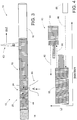
- the frequency modulation device 10 includes a photonic band gap structure 12, coupled at opposite ends to an acoustic pulse generator 14 and to an input/output structure 16.
- the photonic band gap structure 12 may be a photonic band gap fiber that includes a pair of photonic band gap crystals 20 and 22 on opposite sides of a photonic band gap defect 24.
- the photonic band gap defect 24 functions as a frozen shockwave 26 within the photonic band gap structure 12.
- a frozen shockwave as the term is used herein, is defined as a fixed pattern in the material that acts as shockwave, and that has characteristics similar to that a moving shockwave would have if observed as a snapshot frozen time.
- a frozen shockwave is also referred to herein as a stationary shockwave.
- the frozen shockwave 26 is frozen in the sense that it does not move within the photonic band gap structure 12.
- the frozen shockwave 26 remains fixed in spatial location at an interface 28 between the photonic band gap crystals 20 and 22.
- the photonic band gap crystals 20 and 22 are each made of alternating layers of materials with different indices of refraction.
- the first photonic band gap crystal 20 is made of a series of layers 30 of material, while the second photonic band gap crystal 22 is made of layers 32 of material.
- the layers 30 and 32 are generally parallel to the interface 28 between photonic band gap crystals 20 and 22.
- the layers 30 may have the same thickness as the layers 32. As an alternative, the layers 30 may be thinner or thicker than the layers 32.
- the layers 30 and 32 may be made of alternating types of dielectric materials having different indices of refraction. It will be appreciated that a wide variety of suitable dielectric materials may be employed. Silicon and silicon dioxide are examples of suitable materials for the layers 30 and 32.
- the thicknesses of the layers 30 and 32 may be set at any of a wide variety of values, depending upon the wavelength of the radiation involved. Suitable thicknesses would be on the order of the wavelength of the radiation, from fractions of a micron for visible light, to microns for infrared radiation, to on the order of a hundred microns for terahertz-frequency radiation.
- FIG. 2 is a schematic diagram of the photonic band gap structure 12 in the region of the interface 28 between the photonic band gap crystals 22.
- the defect 24 may be a local variation in the pattern of the layers 30 and 32 of the photonic band gap crystals 20 and 22.
- the first photonic band gap crystal 20 includes the layers 30 with alternating layers of two types, layers 30a and 30b.
- the layers 30a are made of a first material having an index of refraction of n 1 .
- the layers 30b are made of a second material having an index of refraction n 2 .
- the second photonic band gap crystal 22 has layers 32 of alternating materials, layers 32a and 32b.
- the layers 32a and 32b may be made of the same material as the layers 30a and 30b.
- the index of refraction between adjacent layers may be a ratio about 2 or greater, although it will be appreciated that a wide variety of different ratios of index of refraction are possible depending upon the desired photonic band gap.
- the layers 30 and 32 may have a dimension d that is about equal to the wavelength of electromagnetic radiation that is being modulated.
- the photonic band gap defect 24 may be a layer having a different thickness, causing a variation in the pattern 30 and 32, and producing the frozen shockwave 26.
- the lattice spacing may be varied in the photonic band gap defect 24.
- This produces a nearly stepwise discontinuity in the properties of the photonic band gap structure 12, although to some extent the material properties, such as the lattice gradient, about the frozen shockwave 26 may have some curve or slope that transitions between the discontinuity and the different values on either side of the frozen shockwave 26.
- the material for the layers 30 and 32 may be any of a wide variety of suitable materials, such as metals, glasses, plastics, or combinations of such materials.
- the crystal regions on either side of the frozen shockwave would be expected to have many more layers of material, such as one hundred or more layers.
- the photonic band gap defect 24 in effect becomes a dynamic squeezed cavity for upward or downward conversion of frequencies of incoming electromagnetic radiation.
- the lattice constant of the photonic band gap structure 12 varies across the interface 28. For a one-dimensional structure this lattice constant is determined by the thickness of the layers 30 and 32 of the photonic band gap crystals 20 and 22. It fixes the band gap on the two sides of the frozen shockwave 26, which determines the amount of frequency modulation that may occur.
- the acoustic pulse generator 14 is in contact with the first photonic band gap crystal 20.
- the pulse generator 14 may include a suitable material for applying a periodic pulse to the first photonic band gap crystal 20.
- the acoustic pulse generator 14 may be a suitable piezoelectric material, for example lead zirconate titanate (PZT).
- a periodic electrical pulse or signal 40 may be sent to the acoustic pulse generator 14 by a suitable driver 36.
- the periodic signal 40 then causes periodic vibrations in the acoustic pulse generator 14, which in turn causes transmission and propagation of a periodic acoustic pulse 44 in the first photonic band gap crystal 20.
- the frequency of the periodic signal 40 may be any or a wide range of frequency, depending upon the desired output frequency rate.
- the periodic signal may have a frequency on the order of 1 Hz to 1 MHz, for example. It will be appreciated that other suitable frequency values may also be used.
- the acoustic pulse 44 propagates through the photonic band gap structure 12 as a compression wave.
- the acoustic pulse 44 reaches the frozen shockwave 26, the frozen shockwave 26 experiences translation and/or compression and decompression in a manner similar to what would occur due to a moving shockwave front.
- the acoustic pulse 44 acts to Doppler shift electromagnetic radiation that impinges on the frozen shockwave 26, upshifting or downshifting the frequency of the incoming electromagnetic radiation.
- the pulse generator 14 may be any of a variety of devices or mechanisms for creating the acoustic pulse 44.
- a laser pulse may be used to generate an acoustic pulse in a dielectric material, so a laser may function as the pulse generator 14.
- a variety of mechanical devices or mechanisms may be used to produce the acoustic pulse 44 in the photonic band gap structure 12. Examples include an impact by an object, an explosion, or an earthquake.
- the device and method used herein may be used to detect impacts, explosions, and/or earthquakes, such as in a sensor.
- An output signal may be examined for modulation consistent with an acoustic pulse caused by an impact, an explosion, or an earthquake.
- the frequency modulation device 10 could be utilized as or in a vibration sensor, where the vibrations are from any of a variety of sources.
- the vibrations themselves could serve as the acoustic pulse 44 that causes frequency modulation to occur in the photonic band gap structure 12.
- the characteristics of the amount and type of modulation that occur could be dependent on the vibration that produces the acoustic pulse 44.
- examination of a modulated output signal may allow information to be obtained regarding the detected vibration.
- the input/output structure 16 may be any of a variety of suitable structures propagating an electromagnetic wave.
- An example of such structure is an optical fiber, made from a suitable plastic or silicon compound.
- the input/output structure 16 may be attached to the second photonic band gap crystal 22 by any of a variety of suitable methods.
- An input signal 50 of electromagnetic radiation proceeds from the input/output structure 16 through the second photonic band gap crystal 22, and to the frozen shockwave 26 at the photonic band gap defect 24 (at the interface 28 between the photonic band gap crystals 20 and 22).
- the incoming electromagnetic radiation 50 is captured and retained in the frozen shockwave 26 for a controlled period of time by the photonic band gaps of the two regions.
- the frequency of the electromagnetic radiation will also be changed, such as from the bottom of a band gap of the structure 12 to the top of the band gap structure 12, or vice versa.
- the amount of frequency conversion in the photonic band gap structure 12 will be tunable by adjusting the band gap size, such as by varying the thickness and/or the composition of the layers 30 and 32.
- the Doppler shifting caused by the acoustic pulse 44 also affects the frequency shifting that occurs at the frozen shockwave 26. Varying the frequency of the acoustic pulse 44 affects the amount of frequency shifting. The bandwidth of the input signals 50 may also be increased or decreased within the frozen shockwave 26.
- the acoustic pulse 44 causes the frequency of the electromagnetic radiation to increase until the radiation is no longer constrained by the band gap defect, at which time it is ejected as outgoing electromagnetic radiation 52.
- the combined action of the frozen shockwave 26 and the acoustic pulse 44 causes modulation of the incoming electromagnetic radiation 50, and ejection of it as the outgoing electromagnetic radiation 52.
- the outgoing radiation 52 may have its frequency shifted from that of the incoming electromagnetic radiation 50.
- the shift in frequency may be as much as about 15-20% of the incoming frequency, for example, depending upon the bandgap sizes.
- the outgoing radiation 52 also may be modulated in ways other than a simple shift in frequency. This may serve to narrow or widen the frequency range of the outgoing radiation 52 relative to that of the incoming radiation 50. Thus narrow band radiation may be converted to wide band radiation, or vice versa.
- Another possible use for the device 10 and method 20 described above is in modulating thermal signature emissions from objects. It will be appreciated that it may be desirable to alter the thermal signature of objects, the wavelengths of radiation naturally given off by an object of a given temperature and composition. Altering the thermal signature makes the object harder to detect, such as by infrared (IR) detection methods. If Planck radiation is used as input electromagnetic radiation to the device 10, the device 10 compresses and shifts the spectrum of the input radiation, which may be useful for thermal signature control.
- IR infrared
- FIG. 3 illustrates use of the device 10 for modulating thermal signature emissions.
- Planck energy 60 thermal energy generated from an object, is the input electromagnetic radiation. It is modulated by the device 10 into narrow band output electromagnetic radiation 62.
- Surface structures that emit thermal IR radiation may be covered with devices that employ the concept of the device 10, in order to modulate emitted radiation in real time.
- Material containing the frozen shockwaves may be part of the surface of the structural material.
- higher frequency radiation may have its frequency relatively unchanged.
- Lower frequency radiation may have its frequency shifted upward more, as much as to the frequency of the higher frequency radiation.
- Two or more frequency modulation devices 10 may be cascaded together (coupled in series) to obtain a greater amount of frequency shift.
- the devices 10 may be coupled together such that the electromagnetic radiation output from one device becomes the input electromagnetic radiation for a second device. This cascading may allow achievement of greater frequency shifts than is possible with use of a single device.
- cascading multiple devices together may allow for greater flexible in other types of frequency modulation, such as narrowing or widening the frequency bandwidth of electromagnetic radiation. Frequency shifting to terahertz (THz) levels may be accomplishable with such cascading.
- THz terahertz
- FIG. 4 Cascading of frozen shockwave devices is illustrated in FIG. 4 , where a cascade system 80 includes a pair of photonic band gap crystal structures 82 and 84, which may be similar in structure to the photonic band gap structure 12 ( FIG. 1 ) described above.
- This intermediate signal 90 is then introduced into the second photonic crystal structure 84, which further increases the frequency to that of an output signal 92.
- cascading such as that shown in the cascade system 80 may involve more than two stages, allowing for greater manipulation of the output signal (such as greater increases or decreases in frequency of the output signal). Timing of the various acoustic pulses may be controlled to coincide with the arrival of input signals at each additional level of a cascading system.
- the device and method have been described above with regard to one-dimensional frequency modulation. It will be appreciated the device and method are applicable to two-dimensional and three-dimensional structures and methods, with suitable modifications. For example, a spherical structure with a central frozen shockwave could be constructed.
Landscapes
- Physics & Mathematics (AREA)
- Nonlinear Science (AREA)
- General Physics & Mathematics (AREA)
- Optics & Photonics (AREA)
- Optical Modulation, Optical Deflection, Nonlinear Optics, Optical Demodulation, Optical Logic Elements (AREA)
Description
- The invention is in the field of photonic crystals and devices for modulating the frequency of electromagnetic rations.
- It is a difficult technical problem to create a device that will shift the frequency of electromagnetic radiation with a significant continuous dynamic range. One prior attempt to address the problem has been to use lasers with nonlinear crystals to generate higher harmonics. However, the generated frequencies are at discrete harmonic steps, rather than having a continuous range.
- Another attempt to approach the problem has been to use Doppler shifting of frequencies. This produces a continuous shifting of frequencies up or down, but only allows for a limited range of frequency shift. In addition, Doppler shifting does not discriminate in its frequency shifting -- all frequencies are shifted by the same amount.
- A third way to shift electromagnetic frequency has been to use cavity tuning to shift frequency. However, cavity tuning may be expensive, and in any event produces only a limited amount of frequency shift.
-
U.S. Patent No. 6,809,856, to Reed et al. , describes a method of modulating frequency of electromagnetic radiation by inputting the radiation into a photonic crystal with a shockwave propagating therethrough. However, the method of propagating a shockwave through a photonic crystal usually destroys the crystal, rendering the method suitable for one-time use only. In addition, the propagating shockwave creates undesirable noise in the radiation output by the photonic crystal. - From the foregoing it may be seen that there is room for improvement in the field of frequency modulation.
- According to an aspect of the invention, a method of modifying frequency of electromagnetic radiation includes the steps of: generating an acoustic pulse in a photonic band gap structure that has an internally constructed stationary shockwave; inputting the electromagnetic radiation into the photonic band gap structure; and modulating the electromagnetic radiation through action of the acoustic pulse while the electromagnetic radiation is retained at the stationary shockwave.
- According to another aspect of the invention, an electromagnetic radiation frequency modulation device includes: a photonic band gap structure having a stationary shockwave therein; and an acoustic pulse generator coupled to the photonic band gap structure.
- To the accomplishment of the foregoing and related ends, the invention comprises the features hereinafter fully described and particularly pointed out in the claims. The following description and the annexed drawings set forth in detail certain illustrative embodiments of the invention. These embodiments are indicative, however, of but a few of the various ways in which the principles of the invention may be employed. Other objects, advantages and novel features of the invention will become apparent from the following detailed description of the invention when considered in conjunction with the drawings.
- In the annexed drawings, which are not necessarily to scale:
-
FIG. 1 is a schematic diagram of frequency modulation device in accordance with an embodiment of the present invention; -
FIG. 2 is a diagram of the photonic band gap structure of the device ofFIG. 1 ; -
FIG. 3 is a schematic diagram of a device for modulating thermal signature emissions; in accordance with another embodiment of the present invention; and -
FIG. 4 is a frequency diagram illustrating yet another embodiment of the present invention, an embodiment involving cascading photonic band gap structures in a frequency modulation device. - A system and method for modulating the frequency of electromagnetic radiation utilizes a frozen shockwave structure in a photonic band gap structure. The frozen shockwave structure provides a discontinuity in lattice constant that functions as a shockwave, and that does not shift its position within the structure. In addition the modulation device or structure includes an acoustic pulse generator, such as a piezoelectric transducer coupled to one end of the photonic band gap structure. The acoustic pulse generator may be driven to produce a periodic pulse in the photonic band gap structure. The frozen shockwave, a defect or discontinuity in the photonic band gap structure, is used to hold incoming electromagnetic radiation in place. The acoustic pulse passing through the photonic band gap structure Doppler shifts the frequency of the radiation, either increasing it or decreasing it. The frequency-shifted radiation is then ejected out of the frozen shockwave portion of the photonic band gap structure. In a one-dimensional configuration, the photonic band gap structure may be made of alternating layers of material having different indices of refraction. Two-dimensional and three-dimensional versions of the photonic band gap structure may also be produced.
- Referring now to
FIG. 1 , a frequency modulation device orsystem 10 is shown. Thefrequency modulation device 10 includes a photonicband gap structure 12, coupled at opposite ends to anacoustic pulse generator 14 and to an input/output structure 16. The photonicband gap structure 12 may be a photonic band gap fiber that includes a pair of photonicband gap crystals band gap defect 24. - The photonic
band gap defect 24 functions as afrozen shockwave 26 within the photonicband gap structure 12. A frozen shockwave, as the term is used herein, is defined as a fixed pattern in the material that acts as shockwave, and that has characteristics similar to that a moving shockwave would have if observed as a snapshot frozen time. A frozen shockwave is also referred to herein as a stationary shockwave. Thefrozen shockwave 26 is frozen in the sense that it does not move within the photonicband gap structure 12. Thefrozen shockwave 26 remains fixed in spatial location at aninterface 28 between the photonicband gap crystals - In the one-dimensional configuration shown in
FIG. 1 , the photonicband gap crystals band gap crystal 20 is made of a series oflayers 30 of material, while the second photonicband gap crystal 22 is made oflayers 32 of material. Thelayers interface 28 between photonicband gap crystals layers 30 may have the same thickness as thelayers 32. As an alternative, thelayers 30 may be thinner or thicker than thelayers 32. - The
layers layers layers -
FIG. 2 is a schematic diagram of the photonicband gap structure 12 in the region of theinterface 28 between the photonicband gap crystals 22. Thedefect 24 may be a local variation in the pattern of thelayers band gap crystals band gap crystal 20 includes thelayers 30 with alternating layers of two types,layers layers 30a are made of a first material having an index of refraction of n1. Thelayers 30b are made of a second material having an index of refraction n2. Similarly, the second photonicband gap crystal 22 haslayers 32 of alternating materials,layers layers layers - The
layers band gap defect 24 may be a layer having a different thickness, causing a variation in thepattern frozen shockwave 26. Thus the lattice spacing may be varied in the photonicband gap defect 24. This produces a nearly stepwise discontinuity in the properties of the photonicband gap structure 12, although to some extent the material properties, such as the lattice gradient, about thefrozen shockwave 26 may have some curve or slope that transitions between the discontinuity and the different values on either side of thefrozen shockwave 26. The material for thelayers - There may be ten or more layers of material in the region of the
frozen shockwave 26. The crystal regions on either side of the frozen shockwave would be expected to have many more layers of material, such as one hundred or more layers. - The photonic
band gap defect 24 in effect becomes a dynamic squeezed cavity for upward or downward conversion of frequencies of incoming electromagnetic radiation. The lattice constant of the photonicband gap structure 12 varies across theinterface 28. For a one-dimensional structure this lattice constant is determined by the thickness of thelayers band gap crystals frozen shockwave 26, which determines the amount of frequency modulation that may occur. - The
acoustic pulse generator 14 is in contact with the first photonicband gap crystal 20. Thepulse generator 14 may include a suitable material for applying a periodic pulse to the first photonicband gap crystal 20. Theacoustic pulse generator 14 may be a suitable piezoelectric material, for example lead zirconate titanate (PZT). A periodic electrical pulse or signal 40 may be sent to theacoustic pulse generator 14 by asuitable driver 36. Theperiodic signal 40 then causes periodic vibrations in theacoustic pulse generator 14, which in turn causes transmission and propagation of a periodicacoustic pulse 44 in the first photonicband gap crystal 20. The frequency of theperiodic signal 40 may be any or a wide range of frequency, depending upon the desired output frequency rate. The periodic signal may have a frequency on the order of 1 Hz to 1 MHz, for example. It will be appreciated that other suitable frequency values may also be used. - The
acoustic pulse 44 propagates through the photonicband gap structure 12 as a compression wave. When theacoustic pulse 44 reaches thefrozen shockwave 26, thefrozen shockwave 26 experiences translation and/or compression and decompression in a manner similar to what would occur due to a moving shockwave front. Theacoustic pulse 44 acts to Doppler shift electromagnetic radiation that impinges on thefrozen shockwave 26, upshifting or downshifting the frequency of the incoming electromagnetic radiation. - The
pulse generator 14 may be any of a variety of devices or mechanisms for creating theacoustic pulse 44. For example, a laser pulse may be used to generate an acoustic pulse in a dielectric material, so a laser may function as thepulse generator 14. A variety of mechanical devices or mechanisms may be used to produce theacoustic pulse 44 in the photonicband gap structure 12. Examples include an impact by an object, an explosion, or an earthquake. Thus it will be appreciated that the device and method used herein may be used to detect impacts, explosions, and/or earthquakes, such as in a sensor. An output signal may be examined for modulation consistent with an acoustic pulse caused by an impact, an explosion, or an earthquake. - More broadly, the
frequency modulation device 10 could be utilized as or in a vibration sensor, where the vibrations are from any of a variety of sources. The vibrations themselves could serve as theacoustic pulse 44 that causes frequency modulation to occur in the photonicband gap structure 12. The characteristics of the amount and type of modulation that occur could be dependent on the vibration that produces theacoustic pulse 44. Thus examination of a modulated output signal may allow information to be obtained regarding the detected vibration. - The input/
output structure 16 may be any of a variety of suitable structures propagating an electromagnetic wave. An example of such structure is an optical fiber, made from a suitable plastic or silicon compound. The input/output structure 16 may be attached to the second photonicband gap crystal 22 by any of a variety of suitable methods. - General operation of the modulation device or
system 10 is now described. Aninput signal 50 of electromagnetic radiation proceeds from the input/output structure 16 through the second photonicband gap crystal 22, and to thefrozen shockwave 26 at the photonic band gap defect 24 (at theinterface 28 between the photonicband gap crystals 20 and 22). The incomingelectromagnetic radiation 50 is captured and retained in thefrozen shockwave 26 for a controlled period of time by the photonic band gaps of the two regions. The frequency of the electromagnetic radiation will also be changed, such as from the bottom of a band gap of thestructure 12 to the top of theband gap structure 12, or vice versa. The amount of frequency conversion in the photonicband gap structure 12 will be tunable by adjusting the band gap size, such as by varying the thickness and/or the composition of thelayers acoustic pulse 44 also affects the frequency shifting that occurs at thefrozen shockwave 26. Varying the frequency of theacoustic pulse 44 affects the amount of frequency shifting. The bandwidth of the input signals 50 may also be increased or decreased within thefrozen shockwave 26. - The
acoustic pulse 44 causes the frequency of the electromagnetic radiation to increase until the radiation is no longer constrained by the band gap defect, at which time it is ejected as outgoingelectromagnetic radiation 52. The combined action of thefrozen shockwave 26 and theacoustic pulse 44 causes modulation of the incomingelectromagnetic radiation 50, and ejection of it as the outgoingelectromagnetic radiation 52. Theoutgoing radiation 52 may have its frequency shifted from that of the incomingelectromagnetic radiation 50. The shift in frequency may be as much as about 15-20% of the incoming frequency, for example, depending upon the bandgap sizes. - The
outgoing radiation 52 also may be modulated in ways other than a simple shift in frequency. This may serve to narrow or widen the frequency range of theoutgoing radiation 52 relative to that of theincoming radiation 50. Thus narrow band radiation may be converted to wide band radiation, or vice versa. - Another possible use for the
device 10 andmethod 20 described above is in modulating thermal signature emissions from objects. It will be appreciated that it may be desirable to alter the thermal signature of objects, the wavelengths of radiation naturally given off by an object of a given temperature and composition. Altering the thermal signature makes the object harder to detect, such as by infrared (IR) detection methods. If Planck radiation is used as input electromagnetic radiation to thedevice 10, thedevice 10 compresses and shifts the spectrum of the input radiation, which may be useful for thermal signature control. -
FIG. 3 illustrates use of thedevice 10 for modulating thermal signature emissions.Planck energy 60, thermal energy generated from an object, is the input electromagnetic radiation. It is modulated by thedevice 10 into narrow band outputelectromagnetic radiation 62. Surface structures that emit thermal IR radiation may be covered with devices that employ the concept of thedevice 10, in order to modulate emitted radiation in real time. Material containing the frozen shockwaves may be part of the surface of the structural material. - In compressing the spectrum of electromagnetic radiation, higher frequency radiation may have its frequency relatively unchanged. Lower frequency radiation may have its frequency shifted upward more, as much as to the frequency of the higher frequency radiation.
- Two or more
frequency modulation devices 10 may be cascaded together (coupled in series) to obtain a greater amount of frequency shift. Thedevices 10 may be coupled together such that the electromagnetic radiation output from one device becomes the input electromagnetic radiation for a second device. This cascading may allow achievement of greater frequency shifts than is possible with use of a single device. In addition, cascading multiple devices together may allow for greater flexible in other types of frequency modulation, such as narrowing or widening the frequency bandwidth of electromagnetic radiation. Frequency shifting to terahertz (THz) levels may be accomplishable with such cascading. - Cascading of frozen shockwave devices is illustrated in
FIG. 4 , where acascade system 80 includes a pair of photonic bandgap crystal structures FIG. 1 ) described above. An inputelectromagnetic radiation signal 86 from anelectromagnetic radiation source 88, such as a laser, is modulated by thefirst photonic crystal 82 to produce anintermediate signal 90 of increased frequency. Thisintermediate signal 90 is then introduced into the secondphotonic crystal structure 84, which further increases the frequency to that of anoutput signal 92. - It will be appreciated that cascading such as that shown in the
cascade system 80 may involve more than two stages, allowing for greater manipulation of the output signal (such as greater increases or decreases in frequency of the output signal). Timing of the various acoustic pulses may be controlled to coincide with the arrival of input signals at each additional level of a cascading system. - It will be appreciated that the structures and methods discussed herein create a wide variety of opportunities modulation of optical signals.
- The device and method have been described above with regard to one-dimensional frequency modulation. It will be appreciated the device and method are applicable to two-dimensional and three-dimensional structures and methods, with suitable modifications. For example, a spherical structure with a central frozen shockwave could be constructed.
- Although the invention has been shown and described with respect to a certain embodiment or embodiments, it is obvious that equivalent alterations and modifications will occur to others skilled in the art upon the reading and understanding of this specification and the annexed drawings. In particular regard to the various functions performed by the above described elements (components, assemblies, devices, compositions, etc.), the terms (including a reference to a "means") used to describe such elements are intended to correspond, unless otherwise indicated, to any element which performs the specified function of the described element (i.e., that is functionally equivalent), even though not structurally equivalent to the disclosed structure which performs the function in the herein illustrated exemplary embodiment or embodiments of the invention.
Claims (11)
- A method of modifying frequency of electromagnetic radiation, the method comprising:generating an acoustic pulse (44) in a photonic band gap structure (12) that has an internally constructed stationary shockwave (26);inputting the electromagnetic radiation into the photonic band gap structure; andmodulating the electromagnetic radiation through action of the acoustic pulse while the electromagnetic radiation is retained at the stationary shockwave.
- The method of claim 1, wherein the modulating includes narrowing the frequency band of the electromagnetic radiation.
- The method of claim 1 or claim 2, wherein the generating includes generating the acoustic pulse with a piezoelectric material (14) that is coupled to the photonic band gap structure.
- The method of any of claims 1 to 3,
wherein the inputting includes inputting thermal radiation from an object operatively coupled to the photonic band gap structure; and
wherein the method of modifying frequency is at least part of a method of altering a thermal signature of the object. - The method of any of claims 1 to 4, wherein the modulating includes modulating the electromagnetic radiation by passing it into one or more additional photonic band gap structures, each having a stationary shockwave therein, wherein the photonic band gap structures are coupled in series.
- An electromagnetic radiation frequency modulation device (12) for carrying out the method of any of claims 1 to 5, the device comprising:the photonic band gap structure having the stationary shockwave therein; and an acoustic pulse generator (14) coupled to the photonic band gap structure.
- The device of claim 6,
wherein the photonic band gap structure is a one-dimensional structure; wherein the photonic band gap structure includes alternating layers of materials (30 and 32) with different indices of refraction; and
wherein the stationary shockwave is a discontinuity (24) in the layers. - The device of claim 6 or claim 7, wherein the acoustic pulse generator includes a piezoelectric material connected to the photonic band gap structure.
- The device of any of claims 6 to 8,
further comprising an optical fiber (16) connected to the photonic band gap structure;
wherein the acoustic pulse generator and the optical fibers are connected to opposite respective ends of the photonic band gap structure. - The device of claim 6, wherein the photonic band gap structure is a multi-dimension structure.
- The device of any of claims 6 to 10,
further comprising an additional photonic band gap structure that includes an additional stationary shockwave;
wherein the photonic gap structures are coupled in series to act sequentially to modulate frequency of input electromagnetic radiation.
Applications Claiming Priority (2)
| Application Number | Priority Date | Filing Date | Title |
|---|---|---|---|
| US11/545,138 US7724420B2 (en) | 2006-10-10 | 2006-10-10 | Frequency modulation structure and method utilizing frozen shockwave |
| PCT/US2007/077841 WO2008045640A1 (en) | 2006-10-10 | 2007-09-07 | Frequency modulation structure and method utilizing frozen shockwave |
Publications (2)
| Publication Number | Publication Date |
|---|---|
| EP2082284A1 EP2082284A1 (en) | 2009-07-29 |
| EP2082284B1 true EP2082284B1 (en) | 2017-12-13 |
Family
ID=38996683
Family Applications (1)
| Application Number | Title | Priority Date | Filing Date |
|---|---|---|---|
| EP07842035.3A Active EP2082284B1 (en) | 2006-10-10 | 2007-09-07 | Frequency modulation structure and method utilizing frozen shockwave |
Country Status (4)
| Country | Link |
|---|---|
| US (1) | US7724420B2 (en) |
| EP (1) | EP2082284B1 (en) |
| JP (1) | JP5558821B2 (en) |
| WO (1) | WO2008045640A1 (en) |
Families Citing this family (4)
| Publication number | Priority date | Publication date | Assignee | Title |
|---|---|---|---|---|
| WO2009036154A1 (en) * | 2007-09-13 | 2009-03-19 | Raytheon Company | Methods and systems for extracting energy from a heat source using photonic crystals with defect cavities |
| US8261557B2 (en) * | 2008-12-05 | 2012-09-11 | Raytheon Company | Heat transfer devices based on thermodynamic cycling of a photonic crystal with coupled resonant defect cavities |
| CA2809746C (en) | 2010-08-27 | 2019-02-12 | Socpra Sciences Et Genie S.E.C. | Mechanical wave generator and method thereof |
| CN115655978B (en) * | 2022-12-09 | 2023-03-21 | 西南交通大学 | An experimental device and method for measuring the evolution of a disturbance shock wave front in a material |
Family Cites Families (24)
| Publication number | Priority date | Publication date | Assignee | Title |
|---|---|---|---|---|
| US4112401A (en) * | 1977-03-14 | 1978-09-05 | Spectron Corporation | Electrical switching apparatus and control system for use therewith |
| JP2890034B2 (en) * | 1996-05-30 | 1999-05-10 | 工業技術院長 | Quantum synthesis device, THz electromagnetic wave generation device, light modulation device, and electron wave modulation device |
| US6002522A (en) * | 1996-06-11 | 1999-12-14 | Kabushiki Kaisha Toshiba | Optical functional element comprising photonic crystal |
| US6014246A (en) * | 1996-11-06 | 2000-01-11 | University Of Pittsburgh Of The Commonwealth System Of Higher Education | Thermally switchable optical devices |
| KR100274075B1 (en) * | 1998-05-09 | 2001-01-15 | 서원석 | Optical fiber grating and optical element using the same |
| US6134369A (en) * | 1999-03-31 | 2000-10-17 | Matsushita Electric Industrial Co. | Compact optical waveguide |
| US6097870A (en) * | 1999-05-17 | 2000-08-01 | Lucent Technologies Inc. | Article utilizing optical waveguides with anomalous dispersion at vis-nir wavelenghts |
| JP3980801B2 (en) * | 1999-09-16 | 2007-09-26 | 株式会社東芝 | Three-dimensional structure and manufacturing method thereof |
| US6674949B2 (en) * | 2000-08-15 | 2004-01-06 | Corning Incorporated | Active photonic crystal waveguide device and method |
| EP1336892A1 (en) * | 2002-02-15 | 2003-08-20 | Paul Drude-Institut für Festkörperelektronik im Forschungsverbund Berlin e.V. | A controllable optical device |
| AU2003224944A1 (en) * | 2002-04-12 | 2003-10-27 | Massachusetts Institute Of Technology | Shock-wave modulation and control of electromagnetic radiation in a photonic crystal |
| JP4569942B2 (en) * | 2002-09-26 | 2010-10-27 | 三菱電機株式会社 | Optical active device |
| WO2004109383A1 (en) * | 2003-06-06 | 2004-12-16 | Nippon Sheet Glass Company, Limited | Optical path conversion element |
| US6813330B1 (en) * | 2003-07-28 | 2004-11-02 | Raytheon Company | High density storage of excited positronium using photonic bandgap traps |
| WO2005022900A2 (en) * | 2003-08-26 | 2005-03-10 | Redshift Systems Corporation | Infrared camera system |
| US7177021B2 (en) * | 2004-09-14 | 2007-02-13 | Hewlett-Packard Development Company, L.P. | Integrated radiation sources and amplifying structures, and methods of using the same |
| US7078697B2 (en) * | 2004-10-07 | 2006-07-18 | Raytheon Company | Thermally powered terahertz radiation source using photonic crystals |
| US7190869B2 (en) * | 2004-10-29 | 2007-03-13 | The Hong Kong Polytechnic University | Two-mode photonic crystal fiber and applications thereof |
| US7257333B2 (en) * | 2005-01-06 | 2007-08-14 | Raytheon Company | Dynamic control of planck radiation in photonic crystals |
| US7304309B2 (en) * | 2005-03-14 | 2007-12-04 | Avraham Suhami | Radiation detectors |
| CA2606439C (en) * | 2005-04-29 | 2016-08-23 | The Board Of Trustees Of The Leland Stanford Junior University | High-sensitivity fiber-compatible optical acoustic sensor |
| US7308163B2 (en) * | 2005-05-10 | 2007-12-11 | Hewlett-Packard Development Company, L.P. | Photonic crystal system and method of controlling/detecting direction of radiation propagation using photonic crystal system |
| US20070047965A1 (en) * | 2005-08-29 | 2007-03-01 | Polaronyx, Inc. | Dynamic amplitude and spectral shaper in fiber laser amplification system |
| US7292740B1 (en) * | 2007-01-18 | 2007-11-06 | Raytheon Company | Apparatus and method for controlling transmission through a photonic band gap crystal |
-
2006
- 2006-10-10 US US11/545,138 patent/US7724420B2/en active Active
-
2007
- 2007-09-07 JP JP2009532486A patent/JP5558821B2/en not_active Expired - Fee Related
- 2007-09-07 WO PCT/US2007/077841 patent/WO2008045640A1/en not_active Ceased
- 2007-09-07 EP EP07842035.3A patent/EP2082284B1/en active Active
Also Published As
| Publication number | Publication date |
|---|---|
| US7724420B2 (en) | 2010-05-25 |
| EP2082284A1 (en) | 2009-07-29 |
| US20080084604A1 (en) | 2008-04-10 |
| WO2008045640A1 (en) | 2008-04-17 |
| JP2010506237A (en) | 2010-02-25 |
| JP5558821B2 (en) | 2014-07-23 |
Similar Documents
| Publication | Publication Date | Title |
|---|---|---|
| Fok et al. | Acoustic metamaterials | |
| Lanzillotti-Kimura et al. | Towards GHz–THz cavity optomechanics in DBR-based semiconductor resonators | |
| US7292740B1 (en) | Apparatus and method for controlling transmission through a photonic band gap crystal | |
| WO2008045640A1 (en) | Frequency modulation structure and method utilizing frozen shockwave | |
| Hladky-Hennion et al. | Acoustic wave localization in one-dimensional Fibonacci phononic structures with mirror symmetry | |
| Santini et al. | Elastic temporal waveguiding | |
| JP2012194555A (en) | Grating based optical parametric oscillator for generating desired optical signals and method of dynamically tuning the oscillator | |
| Wiederhecker et al. | Coherent control of ultrahigh-frequency acoustic resonances in photonic crystal fibers | |
| US7257333B2 (en) | Dynamic control of planck radiation in photonic crystals | |
| Babkina et al. | A new method of acousto-optic image processing and edge enhancement | |
| US7788980B2 (en) | Method for generation of THz frequency radiation and sensing of large amplitude material strain waves in piezoelectric materials | |
| Jin et al. | Multifunctional phononic meta-material actuated by the phase transition in water | |
| Abdulhalim | Reflective polarization conversion Fabry–Perot resonator using omnidirectional mirror of periodic anisotropic stack | |
| US10908477B2 (en) | Ultrasonic/acoustic control of light waves for left-right optical reflection asymmetry | |
| US20250102352A1 (en) | Monolithic optical pressure sensors and transducers | |
| US7209603B2 (en) | Acousto-optical device based on phonon-induced polaritonic band gaps | |
| Yang et al. | Multi-cavity coupling acoustic metamaterials with low-frequency broad band gaps based on negative mass density | |
| KR102595943B1 (en) | Frequency swept source apparatus | |
| Santini et al. | Harnessing Temporal Modulation to Achieve Surface-to-Bulk and Frequency Conversion in Elastic Half-Planes | |
| Trainiti et al. | Time-periodic stiffness modulation in elastic metamaterials for selective wave filtering: theory and experimental investigations | |
| Papanikolaou et al. | Dual photonic–phononic nanocavities for tailoring the acousto-optic interaction | |
| Ward et al. | Phonon-polariton propagation, guidance, and control in bulk and patterned thin film ferroelectric crystals | |
| Fukuma et al. | Synthesis of rejection band profile in ultrasonically induced long-period optical fiber gratings | |
| Rebhi et al. | Dynamics of four-wave-mixing oscillators with quasi-phase-matching | |
| Gevorgyan et al. | Optical properties of chiral photonic crystals with linear profiles of modulation parameters |
Legal Events
| Date | Code | Title | Description |
|---|---|---|---|
| PUAI | Public reference made under article 153(3) epc to a published international application that has entered the european phase |
Free format text: ORIGINAL CODE: 0009012 |
|
| 17P | Request for examination filed |
Effective date: 20090318 |
|
| AK | Designated contracting states |
Kind code of ref document: A1 Designated state(s): AT BE BG CH CY CZ DE DK EE ES FI FR GB GR HU IE IS IT LI LT LU LV MC MT NL PL PT RO SE SI SK TR |
|
| DAX | Request for extension of the european patent (deleted) | ||
| R17P | Request for examination filed (corrected) |
Effective date: 20090318 |
|
| GRAP | Despatch of communication of intention to grant a patent |
Free format text: ORIGINAL CODE: EPIDOSNIGR1 |
|
| INTG | Intention to grant announced |
Effective date: 20170203 |
|
| GRAS | Grant fee paid |
Free format text: ORIGINAL CODE: EPIDOSNIGR3 |
|
| GRAA | (expected) grant |
Free format text: ORIGINAL CODE: 0009210 |
|
| AK | Designated contracting states |
Kind code of ref document: B1 Designated state(s): DE FR GB |
|
| RBV | Designated contracting states (corrected) |
Designated state(s): DE FR GB |
|
| REG | Reference to a national code |
Ref country code: GB Ref legal event code: FG4D |
|
| REG | Reference to a national code |
Ref country code: DE Ref legal event code: R096 Ref document number: 602007053420 Country of ref document: DE |
|
| REG | Reference to a national code |
Ref country code: FR Ref legal event code: PLFP Year of fee payment: 12 |
|
| REG | Reference to a national code |
Ref country code: DE Ref legal event code: R097 Ref document number: 602007053420 Country of ref document: DE |
|
| PLBE | No opposition filed within time limit |
Free format text: ORIGINAL CODE: 0009261 |
|
| STAA | Information on the status of an ep patent application or granted ep patent |
Free format text: STATUS: NO OPPOSITION FILED WITHIN TIME LIMIT |
|
| 26N | No opposition filed |
Effective date: 20180914 |
|
| P01 | Opt-out of the competence of the unified patent court (upc) registered |
Effective date: 20230530 |
|
| PGFP | Annual fee paid to national office [announced via postgrant information from national office to epo] |
Ref country code: DE Payment date: 20240820 Year of fee payment: 18 |
|
| PGFP | Annual fee paid to national office [announced via postgrant information from national office to epo] |
Ref country code: GB Payment date: 20240822 Year of fee payment: 18 |
|
| PGFP | Annual fee paid to national office [announced via postgrant information from national office to epo] |
Ref country code: FR Payment date: 20240820 Year of fee payment: 18 |