EP2078272B1 - Protecting secret information in a programmed electronic device - Google Patents
Protecting secret information in a programmed electronic device Download PDFInfo
- Publication number
- EP2078272B1 EP2078272B1 EP06806092A EP06806092A EP2078272B1 EP 2078272 B1 EP2078272 B1 EP 2078272B1 EP 06806092 A EP06806092 A EP 06806092A EP 06806092 A EP06806092 A EP 06806092A EP 2078272 B1 EP2078272 B1 EP 2078272B1
- Authority
- EP
- European Patent Office
- Prior art keywords
- secret information
- software
- electronic device
- access
- programmed electronic
- Prior art date
- Legal status (The legal status is an assumption and is not a legal conclusion. Google has not performed a legal analysis and makes no representation as to the accuracy of the status listed.)
- Active
Links
- 230000015654 memory Effects 0.000 claims abstract description 42
- 238000000034 method Methods 0.000 claims abstract description 23
- 239000004065 semiconductor Substances 0.000 claims abstract description 14
- 238000010295 mobile communication Methods 0.000 claims description 26
- 230000000903 blocking effect Effects 0.000 claims description 6
- 230000006870 function Effects 0.000 description 6
- 238000010586 diagram Methods 0.000 description 4
- 230000004044 response Effects 0.000 description 2
- 238000012795 verification Methods 0.000 description 2
- 230000003936 working memory Effects 0.000 description 2
- 238000004364 calculation method Methods 0.000 description 1
- 230000008859 change Effects 0.000 description 1
- 238000004891 communication Methods 0.000 description 1
- 230000001419 dependent effect Effects 0.000 description 1
- 230000008569 process Effects 0.000 description 1
Images


Classifications
-
- G—PHYSICS
- G06—COMPUTING; CALCULATING OR COUNTING
- G06F—ELECTRIC DIGITAL DATA PROCESSING
- G06F21/00—Security arrangements for protecting computers, components thereof, programs or data against unauthorised activity
- G06F21/70—Protecting specific internal or peripheral components, in which the protection of a component leads to protection of the entire computer
- G06F21/78—Protecting specific internal or peripheral components, in which the protection of a component leads to protection of the entire computer to assure secure storage of data
-
- G—PHYSICS
- G06—COMPUTING; CALCULATING OR COUNTING
- G06F—ELECTRIC DIGITAL DATA PROCESSING
- G06F21/00—Security arrangements for protecting computers, components thereof, programs or data against unauthorised activity
- G06F21/50—Monitoring users, programs or devices to maintain the integrity of platforms, e.g. of processors, firmware or operating systems
- G06F21/57—Certifying or maintaining trusted computer platforms, e.g. secure boots or power-downs, version controls, system software checks, secure updates or assessing vulnerabilities
- G06F21/575—Secure boot
Definitions
- the present invention generally relates to the field of protecting programmed electronic devices against attacks.
- the present invention relates to the field of protecting secret information in a programmed electronic device.
- Programmable electronic devices have become ubiquitous. In most of these devices, it is desirable to provide at least some level of assurance of the integrity of the software stored in the device. For example, if the programmed electronic device is an embedded device controlling functions of an automotive braking system, any tampering with the software stored in the device may be very dangerous. As another example, if the programmed electronic device is a mobile communication device like, for example, a mobile telephone, unauthorized software may spy out confidential information or may incur unwanted charges or may circumvene restrictions like, for example, digital rights management settings. There is therefore a need in the above-mentioned and other programmed electronic devices that the software executed by the device can be trusted.
- all software that is stored in a mutable memory of the programmed electronic device may be a possible target for an attack.
- Any interface of the programmed electronic device may be used in the attack.
- a manipulated SMS or manipulated WAP data may use a security hole of a browser or message reader to introduce malicious code.
- a user intentionally tries to change the software stored in the programmed electronic device.
- the device is especially vulnerable if the software is stored in a memory that is external to a main semiconductor circuit of the programmed electronic device.
- Such an external memory may be, for example, an EEPROM or FLASH memory that is located on a printed circuit board of the programmed electronic device or on an external memory card.
- the software may be associated with a signature that is or contains a cryptographic hash value of the software.
- a cryptographic hash value is commonly called a Cryptographic Checksum or Message Authentication Code (MAC) or Integrity Check Value.
- the secret component may be a secret key that is used when calculating the cryptographic hash value of the software both during signature creation and during each startup integrity check.
- the cryptographic hash value of the software may be obtained from processing the software - seen as a byte sequence - in a DES block mode operation using the secret key. The last resulting block - or a part thereof - may constitute the cryptographic hash value.
- the secret information - for example, the secret key - must be stored in the programmed electronic device because it is required for the software integrity check each time the device is started up.
- the secret information must be hidden from a possible attacker in order to ensure that the attacker cannot calculate a new signature for any modified software. If the secret information is stored, for example, in a one-time programmable (OTP) memory of the programmed electronic device, there is the risk that an attacker may discover and access the secret information. For example, techniques like the use of malicious software or buffer overflows could potentially be employed to execute code to discover the secret key.
- OTP one-time programmable
- Embodiments of the invention therefore provide an access restriction logic unit that is adapted to allow access to the secret information when starting up the programmed electronic device such that a software integrity check can be conducted using the secret information.
- the access restriction logic is also adapted to block further access to the secret information when such access is no longer needed for the software integrity check.
- the access restriction logic unit of the present invention securely disables any access to the secret information during normal operation of the programmed electronic device, i.e., after the end of the startup phase and the initial software verification phase. Even if an attacker managed to obtain control over the programmed electronic device, the attacker could not access the secret information and could also not execute any system routines - e.g., cryptographic functions - that depend on the secret information.
- the access restriction logic unit may be configured such that it blocks access to the secret information when a predetermined amount of time has passed after starting up the programmed electronic device. This amount of time may be measured, for example, by an analog or digital timer or by a counter that is clocked by a suitable clock signal available within the programmed electronic device.
- the access restriction logic unit may be adapted to be set into an access blocking mode by an external signal or command. For example, a processor unit of the programmed electronic device may disable further access to the secret information by asserting a "disable access" signal or by writing a suitable value into a hardware register of the access restriction logic.
- the secret information is individualized for each programmed electronic device. This further increases the level of protection provided by the present invention because a successful attack would only compromise a single programmed electronic device at each time.
- the secret information may be stored in a one-time programmable memory to ensure that it cannot be altered.
- the programmed electronic device of embodiments of the present invention may be a mobile device and/or a communication device and/or an embedded device.
- Embodiments of the present invention also concern a semiconductor device, which may be part of the programmed electronic device.
- the semiconductor device may be a single integrated circuit or an integrated circuit module.
- the semiconductor device is a base band integrated circuit that is adapted for use in, e.g., a mobile telecommunication apparatus.
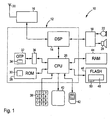
- Fig. 1 shows an example of a programmed electronic device, namely, a mobile communication device 10, in an embodiment of the present invention.
- the mobile communication device 10 may be, for example, a mobile telephone.
- the present invention is not restricted to mobile communication devices, but can be used in connection with all kinds of programmed electronic devices that must provide some level of protection against execution of unauthorized software.
- the programmed electronic device of the present invention generally comprises a semiconductor device, which may be formed of one or more integrated semiconductor circuits.
- the semiconductor device is a base band integrated circuit 12 of the mobile communication device 10.
- the base band integrated circuit 12 comprises a digital signal processor 14 (DSP) that is connected to a high frequency unit 16 and a voice frequency unit 18.
- DSP digital signal processor
- the high frequency unit 16 is connected to an antenna 20 and serves for sending and receiving modulated radio signals.
- the voice frequency unit 18 is connected to a microphone 22 and a speaker 24 for receiving and transmitting voice signals from and to a user of the mobile communication device 10.
- a processor unit 26 interfaces with a variety of components internal or external to the base band integrated circuit 12.
- the internal components include a program memory 28 that contains a number of program routines, including startup code 30.
- the program memory 28 may, for example, be a mask-programmed read-only memory (ROM) or another non-changeable memory.
- a further internal component of the base band integrated circuit 12 is a data memory 32 that contains various configuration values and other data items for operation of the mobile communication device 10. These data items include secret information 34, whose role will be explained in detail below.
- the data memory 32 may, for example, be a one-time programmable memory (OTP).
- the processor unit 26 accesses the data memory 32 - or at least the portion of the data memory 32 that stores the secret information 34 - via an access restriction logic unit 36.
- the access restriction logic unit 36 has at least two modes of operation. A first mode of operation is automatically set when the mobile communication device 10 starts up. In this mode, the processor unit 26 is allowed to access the secret information 34. A second mode of operation blocks the processor unit 26 from accessing the secret information 34.
- the access restriction logic unit 36 enters the second mode of operation in response to a signal or command from the processor unit 26, while in other embodiments, the access restriction logic unit 36 enters the second mode of operation automatically after a predetermined time - e.g., some milliseconds - has elapsed after start up of the mobile communication device 10.
- the blocking function of the access restriction logic unit 36 in the second mode of operation may be effective just with respect to the portion of the data memory 32 that stores the secret information 34, while in other embodiments the blocking function may extend to further portions of the data memory 32.
- the access restriction logic unit 36 will stay in the second mode of operation as long as the mobile communication device 10 is powered on. In other words, there is no way of resetting the access restriction logic unit 36 to its first mode of operation, other than switching off and re-starting the mobile communication device 10.
- the processor unit 26 is further connected to a number of components that are external to the base band integrated circuit 12. These components include a keypad 38, a display 40, a subscriber identity module 42 (SIM), a working memory 44 and a non-trusted memory 46.
- the working memory 44 may, for example, be a volatile read/write memory (RAM).
- the non-trusted memory 46 may, for example, be an electrically erasable programmable read-only memory (EEPROM) or a FLASH memory.
- the non-trusted memory 46 contains software 48 that is intended for execution by the processor unit 26. This software 48 may, for example, be a part of an operating system of the mobile communication device 10 or an application program.
- the software 48 stored in the non-trusted memory 46 is associated with a signature 50 that, in the present embodiment, represents a hash value of the "correct", i.e., non-manipulated, software 48.
- This signature 50 is determined by the manufacturer of the software 48 and/or the mobile communication device 10, and the signature 50 is written into the non-trusted memory 46 together with the software 48.
- the validity of the software 48 is checked when starting up the mobile communication device 10 by re-calculating the hash value of the software 48. If the software 48 has not been tampered with, then the re-calculated hash value and the signature 50 will be identical. On the other hand, if the software 48 has been modified or replaced by different program code, then the re-calculated hash value will differ from the signature 50, and the verification will fail. It is apparent that the startup code 30 that performs this integrity check must be trusted. In the present embodiment, tampering with the startup code 30 is prevented by storing the startup code 30 in an immutable memory like, for example, the mask-programmed program memory 28.
- the hash value is computed as a cryptographic hash value by a cryptographic hashing method both when generating the signature 50 and when performing the startup validity check.
- a hashing method that is based on a symmetric cryptographic algorithm is used. For example, this may be the MD5 hashing method or a hashing method of the SHA-1 family or the AES hashing method. The above and other hashing methods are well known in the art.
- a secret key to ensure that an unauthorized attacker cannot obtain a valid signature 50 for a modified piece of software 48.
- this secret key is stored as the secret information 34 in the data memory 32.
- the secret key may comprise additional or less information than the secret information 34, as long as the secret information 34 enables the cryptographic hashing method to generate the proper hash value of the software 48.
- a single secret key is used for a plurality of mobile communication devices 10.
- the secret key is individualized and is therefore specific to a single mobile communication device 10 and the signature 50 contained therein.
- Fig. 2 shows the sequence of events and calculation steps that take place during the phase of starting up the mobile communication device 10.
- a startup event 52 triggers execution of the startup code 30 stored in the immutable program memory 28.
- the processor unit 36 Under control of the startup code 30, the processor unit 36 first reads out the secret information 34 - representing a secret hashing key - from the data memory 32.
- the access restriction logic unit 36 allows this access to the data memory 32 because the access restriction logic unit 36 has been set to its first mode of operation by the startup event 52 or by a hardware power up signal.
- the dashed box in Fig. 2 represents the integrity check phase 54.
- the processor unit 26 reads the program code - seen as a byte sequence - that represents the software 48 from the non-trusted memory 46.
- the processor unit 26 then verifies the signature 50 by calculating the hash value of the program code and comparing this newly calculated hash value with the value of the signature 50.
- the access restriction logic unit 36 is set to its second mode of operation during the integrity check phase 54. As a consequence, the access restriction logic unit 36 blocks all further attempts to access the secret information 34. Because the access restriction logic unit 36 is implemented as a hardware component, it cannot be circumvened by any software-based attack. Furthermore, the access restriction logic unit 36 in the present embodiment is designed such that it cannot be switched back from the second - i.e., blocking - mode of operation to the first mode of operation as long as the mobile communication device 10 remains powered on.
- the software 48 stored in the non-trusted memory 46 is started, and processing of the startup code 30 terminates. On the other hand, if the integrity check fails (not shown in Fig. 2 ), then an appropriate error message is generated, and the software 48 is not executed.
- the step of disabling further access to the secret information by switching the access restriction logic unit 36 to its second mode of operation is shown at the end of the integrity check phase 54.
- the access restriction logic unit 36 may be switched to its second mode of operation immediately after reading out the key from the data memory 32.
- the read-out operation may at the same time trigger the access restriction logic unit 36 to switch into the blocking mode.
- the access restriction logic unit 36 is time controlled such that the switch to the second mode of operation will be made, for example, a few milliseconds after the startup event 52, i.e., at some time during the integrity check phase 54.
- Fig. 3 and Fig. 4 show an example of an access restriction logic unit 36 that is controlled by a signal from the processor unit 26.
- Fig. 3 depicts the first mode of operation in which the processor unit 26 is allowed to access the secret information through the access restriction logic unit 36; this is symbolized by the arrow 56.
- the access restriction logic unit 36 switches to the second mode of operation shown in Fig. 4 .
- the access restriction logic unit 36 blocks any access to the secret information 34.
- a self holding logic of the access restriction logic unit 36 ensures that the access restriction logic unit 36 will remain in the second mode of operation as long as the mobile communication device 10 remains powered on.
- Fig. 5 and Fig. 6 are similar to Fig. 3 and Fig. 4 , but show an alternative embodiment in which the access restriction logic unit 36 is essentially time-controlled.
- Fig. 5 depicts the first mode of operation in which the secret information 34 is accessible.
- a counter 58 is initially set to a predetermined value N and counts down, driven by a CPU clock or another suitable clock signal. The counter 58 is configured such that the counting stops when the counter 58 reaches zero. At this time the access restriction logic unit 36 is switched to its second mode of operation where all further access to the secret information 34 is disabled.
- the disable access control signal of Fig. 3 can be generated by another element of the mobile communication device 10, including the access restriction logic unit 36 itself, in response to an appropriate event.
- the counter 58 of Fig. 5 may be replaced by any other timer that causes the access restriction logic unit 36 to switch to the second mode of operation at an appropriate time. Accordingly, the scope of the invention should be determined not by the embodiments illustrated, but by the appended claims and their legal equivalents.
Landscapes
- Engineering & Computer Science (AREA)
- Computer Security & Cryptography (AREA)
- Computer Hardware Design (AREA)
- Theoretical Computer Science (AREA)
- Software Systems (AREA)
- General Engineering & Computer Science (AREA)
- Physics & Mathematics (AREA)
- General Physics & Mathematics (AREA)
- Storage Device Security (AREA)
Abstract
Description
- The present invention generally relates to the field of protecting programmed electronic devices against attacks. In particular, the present invention relates to the field of protecting secret information in a programmed electronic device.
- Programmed electronic devices have become ubiquitous. In most of these devices, it is desirable to provide at least some level of assurance of the integrity of the software stored in the device. For example, if the programmed electronic device is an embedded device controlling functions of an automotive braking system, any tampering with the software stored in the device may be very dangerous. As another example, if the programmed electronic device is a mobile communication device like, for example, a mobile telephone, unauthorized software may spy out confidential information or may incur unwanted charges or may circumvene restrictions like, for example, digital rights management settings. There is therefore a need in the above-mentioned and other programmed electronic devices that the software executed by the device can be trusted.
- In principle, all software that is stored in a mutable memory of the programmed electronic device may be a possible target for an attack. Any interface of the programmed electronic device may be used in the attack. For example, a manipulated SMS or manipulated WAP data may use a security hole of a browser or message reader to introduce malicious code. It is also possible that a user intentionally tries to change the software stored in the programmed electronic device. In this case, the device is especially vulnerable if the software is stored in a memory that is external to a main semiconductor circuit of the programmed electronic device. Such an external memory may be, for example, an EEPROM or FLASH memory that is located on a printed circuit board of the programmed electronic device or on an external memory card.
- It is known in the field of mobile telephones to check the integrity of the application software when starting up the device. A successful integrity check indicates that the software has not been altered or tampered with and can therefore be trusted. For example, the software may be associated with a signature that is or contains a cryptographic hash value of the software. Such a hash value is commonly called a Cryptographic Checksum or Message Authentication Code (MAC) or Integrity Check Value. During the process of starting up the telephone, the cryptographic hash value of the software is re-computed and compared with the value stored in the signature. If both values coincide, the integrity check succeeds, and the software is deemed to be acceptable for execution.
- It is important that the cryptographic hash value contains a secret component. Otherwise, an attacker could easily build a new signature matching any modified software. The secret component may be a secret key that is used when calculating the cryptographic hash value of the software both during signature creation and during each startup integrity check. For example, the cryptographic hash value of the software may be obtained from processing the software - seen as a byte sequence - in a DES block mode operation using the secret key. The last resulting block - or a part thereof - may constitute the cryptographic hash value.
- The secret information - for example, the secret key - must be stored in the programmed electronic device because it is required for the software integrity check each time the device is started up. On the other hand, the secret information must be hidden from a possible attacker in order to ensure that the attacker cannot calculate a new signature for any modified software. If the secret information is stored, for example, in a one-time programmable (OTP) memory of the programmed electronic device, there is the risk that an attacker may discover and access the secret information. For example, techniques like the use of malicious software or buffer overflows could potentially be employed to execute code to discover the secret key.
- Even if the attacker cannot access the secret information directly, there is still the risk that the attacker may manage to execute software or hardware functions of the programmed electronic device that in turn access and use the secret information. For example, such functions could be used by the attacker to encrypt or decrypt data or to generate a valid signature for modified software.
- It is therefore an object of the present invention to provide a technique for securely protecting secret information - for example, a secret key - in a programmed electronic device. It is a further object of the present invention to provide a technique that allows verification of the integrity of software installed in the programmed electronic device with improved resistance against attacks.
- The present invention is defined by the independent claims. The dependent claims concern optional features of some embodiments of the invention.
- The present invention is based on the fundamental idea that the secret information, which is intended for use in the software integrity check, only needs to be accessed during the phase of starting up the programmed electronic device. Embodiments of the invention therefore provide an access restriction logic unit that is adapted to allow access to the secret information when starting up the programmed electronic device such that a software integrity check can be conducted using the secret information. In these embodiments, the access restriction logic is also adapted to block further access to the secret information when such access is no longer needed for the software integrity check.
- The access restriction logic unit of the present invention securely disables any access to the secret information during normal operation of the programmed electronic device, i.e., after the end of the startup phase and the initial software verification phase. Even if an attacker managed to obtain control over the programmed electronic device, the attacker could not access the secret information and could also not execute any system routines - e.g., cryptographic functions - that depend on the secret information.
- In different embodiments of the present invention, there may be different criteria for determining when the secret information is no longer needed and hence further access to it may be blocked. For example, the access restriction logic unit may be configured such that it blocks access to the secret information when a predetermined amount of time has passed after starting up the programmed electronic device. This amount of time may be measured, for example, by an analog or digital timer or by a counter that is clocked by a suitable clock signal available within the programmed electronic device. Alternatively or additionally, the access restriction logic unit may be adapted to be set into an access blocking mode by an external signal or command. For example, a processor unit of the programmed electronic device may disable further access to the secret information by asserting a "disable access" signal or by writing a suitable value into a hardware register of the access restriction logic.
- In some embodiments the secret information is individualized for each programmed electronic device. This further increases the level of protection provided by the present invention because a successful attack would only compromise a single programmed electronic device at each time. The secret information may be stored in a one-time programmable memory to ensure that it cannot be altered.
- The programmed electronic device of embodiments of the present invention may be a mobile device and/or a communication device and/or an embedded device. Embodiments of the present invention also concern a semiconductor device, which may be part of the programmed electronic device. For example, the semiconductor device may be a single integrated circuit or an integrated circuit module. In some embodiments, the semiconductor device is a base band integrated circuit that is adapted for use in, e.g., a mobile telecommunication apparatus.
- Further features, objects and advantages of the invention will become apparent when studying the following detailed description, in connection with the annexed drawings, in which:
-
Fig. 1 is a schematic block diagram of a mobile communication device according to one embodiment of the present invention, -
Fig. 2 is a sequence diagram of a method that is performed when starting up the mobile communication device shown inFig. 1 , -
Fig. 3 and Fig. 4 are schematic block diagrams of components of the mobile communication device ofFig. 1 in a first and second mode of operation of an access restriction logic unit, respectively, and -
Fig. 5 and Fig. 6 are schematic block diagrams similar to those ofFig. 3 and Fig. 4 in an alternative embodiment. -
Fig. 1 shows an example of a programmed electronic device, namely, amobile communication device 10, in an embodiment of the present invention. Themobile communication device 10 may be, for example, a mobile telephone. However, the present invention is not restricted to mobile communication devices, but can be used in connection with all kinds of programmed electronic devices that must provide some level of protection against execution of unauthorized software. - The programmed electronic device of the present invention generally comprises a semiconductor device, which may be formed of one or more integrated semiconductor circuits. In the present example embodiment, the semiconductor device is a base band integrated
circuit 12 of themobile communication device 10. As it is well known in the art, the base band integratedcircuit 12 comprises a digital signal processor 14 (DSP) that is connected to ahigh frequency unit 16 and avoice frequency unit 18. Thehigh frequency unit 16 is connected to anantenna 20 and serves for sending and receiving modulated radio signals. Thevoice frequency unit 18 is connected to amicrophone 22 and aspeaker 24 for receiving and transmitting voice signals from and to a user of themobile communication device 10. - A processor unit 26 (CPU) interfaces with a variety of components internal or external to the base band integrated
circuit 12. The internal components include aprogram memory 28 that contains a number of program routines, includingstartup code 30. Theprogram memory 28 may, for example, be a mask-programmed read-only memory (ROM) or another non-changeable memory. A further internal component of the base band integratedcircuit 12 is adata memory 32 that contains various configuration values and other data items for operation of themobile communication device 10. These data items includesecret information 34, whose role will be explained in detail below. Thedata memory 32 may, for example, be a one-time programmable memory (OTP). - The
processor unit 26 accesses the data memory 32 - or at least the portion of thedata memory 32 that stores the secret information 34 - via an accessrestriction logic unit 36. As it will be explained in more detail below, the accessrestriction logic unit 36 has at least two modes of operation. A first mode of operation is automatically set when themobile communication device 10 starts up. In this mode, theprocessor unit 26 is allowed to access thesecret information 34. A second mode of operation blocks theprocessor unit 26 from accessing thesecret information 34. - In some embodiments, the access
restriction logic unit 36 enters the second mode of operation in response to a signal or command from theprocessor unit 26, while in other embodiments, the accessrestriction logic unit 36 enters the second mode of operation automatically after a predetermined time - e.g., some milliseconds - has elapsed after start up of themobile communication device 10. - In some embodiments, the blocking function of the access
restriction logic unit 36 in the second mode of operation may be effective just with respect to the portion of thedata memory 32 that stores thesecret information 34, while in other embodiments the blocking function may extend to further portions of thedata memory 32. In many embodiments, the accessrestriction logic unit 36 will stay in the second mode of operation as long as themobile communication device 10 is powered on. In other words, there is no way of resetting the accessrestriction logic unit 36 to its first mode of operation, other than switching off and re-starting themobile communication device 10. - The
processor unit 26 is further connected to a number of components that are external to the base band integratedcircuit 12. These components include a keypad 38, adisplay 40, a subscriber identity module 42 (SIM), a workingmemory 44 and anon-trusted memory 46. The workingmemory 44 may, for example, be a volatile read/write memory (RAM). Thenon-trusted memory 46 may, for example, be an electrically erasable programmable read-only memory (EEPROM) or a FLASH memory. Thenon-trusted memory 46 containssoftware 48 that is intended for execution by theprocessor unit 26. Thissoftware 48 may, for example, be a part of an operating system of themobile communication device 10 or an application program. - The
software 48 stored in thenon-trusted memory 46 is associated with asignature 50 that, in the present embodiment, represents a hash value of the "correct", i.e., non-manipulated,software 48. Thissignature 50 is determined by the manufacturer of thesoftware 48 and/or themobile communication device 10, and thesignature 50 is written into thenon-trusted memory 46 together with thesoftware 48. - The validity of the
software 48 is checked when starting up themobile communication device 10 by re-calculating the hash value of thesoftware 48. If thesoftware 48 has not been tampered with, then the re-calculated hash value and thesignature 50 will be identical. On the other hand, if thesoftware 48 has been modified or replaced by different program code, then the re-calculated hash value will differ from thesignature 50, and the verification will fail. It is apparent that thestartup code 30 that performs this integrity check must be trusted. In the present embodiment, tampering with thestartup code 30 is prevented by storing thestartup code 30 in an immutable memory like, for example, the mask-programmedprogram memory 28. - In the present embodiment, the hash value is computed as a cryptographic hash value by a cryptographic hashing method both when generating the
signature 50 and when performing the startup validity check. In many embodiments, a hashing method that is based on a symmetric cryptographic algorithm is used. For example, this may be the MD5 hashing method or a hashing method of the SHA-1 family or the AES hashing method. The above and other hashing methods are well known in the art. - All of the above cryptographic hashing methods use a secret key to ensure that an unauthorized attacker cannot obtain a
valid signature 50 for a modified piece ofsoftware 48. In the present embodiment, this secret key is stored as thesecret information 34 in thedata memory 32. In other embodiments, the secret key may comprise additional or less information than thesecret information 34, as long as thesecret information 34 enables the cryptographic hashing method to generate the proper hash value of thesoftware 48. In some embodiments a single secret key is used for a plurality ofmobile communication devices 10. However, in the present embodiment, the secret key is individualized and is therefore specific to a singlemobile communication device 10 and thesignature 50 contained therein. -
Fig. 2 shows the sequence of events and calculation steps that take place during the phase of starting up themobile communication device 10. Astartup event 52 triggers execution of thestartup code 30 stored in theimmutable program memory 28. Under control of thestartup code 30, theprocessor unit 36 first reads out the secret information 34 - representing a secret hashing key - from thedata memory 32. The accessrestriction logic unit 36 allows this access to thedata memory 32 because the accessrestriction logic unit 36 has been set to its first mode of operation by thestartup event 52 or by a hardware power up signal. - The dashed box in
Fig. 2 represents theintegrity check phase 54. In this phase, theprocessor unit 26 reads the program code - seen as a byte sequence - that represents thesoftware 48 from thenon-trusted memory 46. Theprocessor unit 26 then verifies thesignature 50 by calculating the hash value of the program code and comparing this newly calculated hash value with the value of thesignature 50. - The access
restriction logic unit 36 is set to its second mode of operation during theintegrity check phase 54. As a consequence, the accessrestriction logic unit 36 blocks all further attempts to access thesecret information 34. Because the accessrestriction logic unit 36 is implemented as a hardware component, it cannot be circumvened by any software-based attack. Furthermore, the accessrestriction logic unit 36 in the present embodiment is designed such that it cannot be switched back from the second - i.e., blocking - mode of operation to the first mode of operation as long as themobile communication device 10 remains powered on. - If the integrity check has been completed successfully, then the
software 48 stored in thenon-trusted memory 46 is started, and processing of thestartup code 30 terminates. On the other hand, if the integrity check fails (not shown inFig. 2 ), then an appropriate error message is generated, and thesoftware 48 is not executed. - In
Fig. 2 , the step of disabling further access to the secret information by switching the accessrestriction logic unit 36 to its second mode of operation is shown at the end of theintegrity check phase 54. However, in other embodiments the accessrestriction logic unit 36 may be switched to its second mode of operation immediately after reading out the key from thedata memory 32. For example, the read-out operation may at the same time trigger the accessrestriction logic unit 36 to switch into the blocking mode. In other embodiments, the accessrestriction logic unit 36 is time controlled such that the switch to the second mode of operation will be made, for example, a few milliseconds after thestartup event 52, i.e., at some time during theintegrity check phase 54. -
Fig. 3 and Fig. 4 show an example of an accessrestriction logic unit 36 that is controlled by a signal from theprocessor unit 26.Fig. 3 depicts the first mode of operation in which theprocessor unit 26 is allowed to access the secret information through the accessrestriction logic unit 36; this is symbolized by thearrow 56. When theprocessor unit 26 asserts the disable access control signal shown inFig. 3 , the accessrestriction logic unit 36 switches to the second mode of operation shown inFig. 4 . Here, the accessrestriction logic unit 36 blocks any access to thesecret information 34. A self holding logic of the accessrestriction logic unit 36 ensures that the accessrestriction logic unit 36 will remain in the second mode of operation as long as themobile communication device 10 remains powered on. -
Fig. 5 and Fig. 6 are similar toFig. 3 and Fig. 4 , but show an alternative embodiment in which the accessrestriction logic unit 36 is essentially time-controlled. Again,Fig. 5 depicts the first mode of operation in which thesecret information 34 is accessible. Acounter 58 is initially set to a predetermined value N and counts down, driven by a CPU clock or another suitable clock signal. Thecounter 58 is configured such that the counting stops when thecounter 58 reaches zero. At this time the accessrestriction logic unit 36 is switched to its second mode of operation where all further access to thesecret information 34 is disabled. - The particulars contained in the above description of sample embodiments should not be construed as limitations of the scope of the invention, but rather as exemplifications of some embodiments thereof. For example, in alternative embodiments, the disable access control signal of
Fig. 3 can be generated by another element of themobile communication device 10, including the accessrestriction logic unit 36 itself, in response to an appropriate event. As another example, thecounter 58 ofFig. 5 may be replaced by any other timer that causes the accessrestriction logic unit 36 to switch to the second mode of operation at an appropriate time. Accordingly, the scope of the invention should be determined not by the embodiments illustrated, but by the appended claims and their legal equivalents.
Claims (15)
- A method for protecting secret information (34) in a programmed electronic device, the programmed electronic device comprising a non-trusted memory (46) containing software (48), a data memory (32) containing the secret information (34), and an access restriction logic unit (36) that is adapted to allow or block access to the secret information (34), the secret information (34) being adapted to be used for verifying the integrity of the software (48), the method comprising:- when starting up the programmed electronic device, the access restriction logic unit (36) allowing access to the secret information (34),- accessing the secret information (34) for use in verifying the integrity of the software (48), and- the access restriction logic unit (36) blocking further access to the secret information (34) when a predetermined amount of time has passed after starting up the programmed electronic device.
- The method of claim 1, further comprising verifying the integrity of the software (48) using the secret information (34).
- The method of claim 2, wherein verifying the integrity of the software (48) comprises:- computing a hash value of the software (48) using a secret key related to the secret information (34), and- comparing the computed hash value with a predetermined signature (50) associated with the software (48).
- The method of any one of claims 1 - 3, wherein the predetermined amount of time is measured as a predetermined number of clock cycles.
- The method of claim 4, wherein the programmed electronic device comprises a processor unit (26) that accesses the secret information (34) and thereafter causes the access restriction logic unit (36) to block further access to the secret information (34).
- The method of any one of claims 1 - 5, wherein the secret information (34) is individualized for each programmed electronic device.
- The method of any one of claims 1 - 6, wherein the programmed electronic device is a mobile communication device (10).
- The method of any one of claims 1 - 7, wherein the software (48) is executed in the programmed electronic device only if the integrity of the software (48) has been verified.
- A semiconductor device, comprising:- a data memory (32) storing secret information (34),- a program memory (28) storing startup code (30),- a processor unit (26) adapted for executing the startup code (30), the startup code (30) being adapted to cause the processor unit (26) to access the secret information (34) in the data memory (32) for use in verifying the integrity of software (48) to be executed by the processor unit (26), and- an access restriction logic unit (36) that allows the processor unit (26) to access the secret information (34) after starting up the semiconductor device and blocks access to the secret information (34) after the processor unit (26) has accessed the secret information (34),
wherein the access restriction logic unit (36) is adapted to block access to the secret information (34) when a predetermined amount of time has passed after starting up the semiconductor device. - The semiconductor device of claim 9, wherein the semiconductor device is a base band integrated circuit (12) for a mobile communication device (10).
- The device of claim 9 or claim 10, wherein the startup code (30) is further adapted to cause the processor unit (26) to verify the integrity of the software (48) using the secret information (34).
- The device of claim 11, wherein the startup code (30) is further adapted to cause the processor unit (26) to compute a hash value of the software (48) using a secret key related to the secret information (34), and wherein the startup code (30) is further adapted to cause the processor unit (26) to compare the computed hash value with a predetermined signature (50) associated with the software (48).
- Use of a semiconductor device according to any one of claims 9 - 12 in a programmed electronic device, the programmed electronic device comprising:- a non-trusted memory (46) storing the software (48).
- The use of claims 13, wherein the software (48) is executed in the programmed electronic device only if the integrity of the software (48) has been verified successfully.
- The use of any one of claims 13 and 14, wherein the programmed electronic device is a mobile communication device (10).
Applications Claiming Priority (1)
| Application Number | Priority Date | Filing Date | Title |
|---|---|---|---|
| PCT/EP2006/009690 WO2008040377A1 (en) | 2006-10-06 | 2006-10-06 | Protecting secret information in a programmed electronic device |
Publications (2)
| Publication Number | Publication Date |
|---|---|
| EP2078272A1 EP2078272A1 (en) | 2009-07-15 |
| EP2078272B1 true EP2078272B1 (en) | 2010-12-15 |
Family
ID=38282830
Family Applications (1)
| Application Number | Title | Priority Date | Filing Date |
|---|---|---|---|
| EP06806092A Active EP2078272B1 (en) | 2006-10-06 | 2006-10-06 | Protecting secret information in a programmed electronic device |
Country Status (5)
| Country | Link |
|---|---|
| US (1) | US8528108B2 (en) |
| EP (1) | EP2078272B1 (en) |
| AT (1) | ATE491999T1 (en) |
| DE (1) | DE602006019011D1 (en) |
| WO (1) | WO2008040377A1 (en) |
Families Citing this family (21)
| Publication number | Priority date | Publication date | Assignee | Title |
|---|---|---|---|---|
| EP2078272B1 (en) | 2006-10-06 | 2010-12-15 | Agere Systems, Inc. | Protecting secret information in a programmed electronic device |
| WO2008071222A1 (en) | 2006-12-15 | 2008-06-19 | Agere Systems Inc. | Protecting a programmable memory against unauthorized modification |
| US9203620B1 (en) * | 2008-01-28 | 2015-12-01 | Emc Corporation | System, method and apparatus for secure use of cryptographic credentials in mobile devices |
| JP5466645B2 (en) * | 2008-08-22 | 2014-04-09 | インターナショナル・ビジネス・マシーンズ・コーポレーション | Storage device, information processing device, and program |
| US20120174206A1 (en) * | 2010-12-31 | 2012-07-05 | Alpine Access, Inc. | Secure computing environment |
| CA2762465A1 (en) * | 2011-02-11 | 2012-08-11 | Research In Motion Limited | System and method for managing access to a communication network |
| US8983855B1 (en) | 2011-05-16 | 2015-03-17 | Mckesson Financial Holdings | Systems and methods for evaluating adherence to a project control process |
| US8261085B1 (en) * | 2011-06-22 | 2012-09-04 | Media Patents, S.L. | Methods, apparatus and systems to improve security in computer systems |
| US8595510B2 (en) | 2011-06-22 | 2013-11-26 | Media Patents, S.L. | Methods, apparatus and systems to improve security in computer systems |
| US8181035B1 (en) | 2011-06-22 | 2012-05-15 | Media Patents, S.L. | Methods, apparatus and systems to improve security in computer systems |
| US20130061328A1 (en) * | 2011-09-06 | 2013-03-07 | Broadcom Corporation | Integrity checking system |
| US9280653B2 (en) * | 2011-10-28 | 2016-03-08 | GM Global Technology Operations LLC | Security access method for automotive electronic control units |
| US20130173469A1 (en) * | 2012-01-03 | 2013-07-04 | Intel Mobile Communications GmbH | Chip customization techniques |
| CN103294941B (en) * | 2012-02-22 | 2016-04-20 | 腾讯科技(深圳)有限公司 | The method of access private space and mobile device |
| US8650645B1 (en) * | 2012-03-29 | 2014-02-11 | Mckesson Financial Holdings | Systems and methods for protecting proprietary data |
| US8844026B2 (en) | 2012-06-01 | 2014-09-23 | Blackberry Limited | System and method for controlling access to secure resources |
| US9843624B1 (en) * | 2013-06-13 | 2017-12-12 | Pouya Taaghol | Distributed software defined networking |
| US9088574B2 (en) * | 2013-07-18 | 2015-07-21 | International Business Machines Corporation | Subscriber identity module-based authentication of a wireless device and applications stored thereon |
| US9460567B2 (en) * | 2014-07-29 | 2016-10-04 | GM Global Technology Operations LLC | Establishing secure communication for vehicle diagnostic data |
| US9916452B2 (en) * | 2016-05-18 | 2018-03-13 | Microsoft Technology Licensing, Llc | Self-contained cryptographic boot policy validation |
| US11068600B2 (en) * | 2018-05-21 | 2021-07-20 | Kct Holdings, Llc | Apparatus and method for secure router with layered encryption |
Family Cites Families (28)
| Publication number | Priority date | Publication date | Assignee | Title |
|---|---|---|---|---|
| US5421006A (en) * | 1992-05-07 | 1995-05-30 | Compaq Computer Corp. | Method and apparatus for assessing integrity of computer system software |
| FR2720532B1 (en) * | 1994-05-25 | 1997-09-12 | Vincent Lorphelin | Secure software rental system with memory card. |
| FR2727227B1 (en) * | 1994-11-17 | 1996-12-20 | Schlumberger Ind Sa | ACTIVE SECURITY DEVICE WITH ELECTRONIC MEMORY |
| US5943423A (en) * | 1995-12-15 | 1999-08-24 | Entegrity Solutions Corporation | Smart token system for secure electronic transactions and identification |
| US8225089B2 (en) * | 1996-12-04 | 2012-07-17 | Otomaku Properties Ltd., L.L.C. | Electronic transaction systems utilizing a PEAD and a private key |
| US6304970B1 (en) * | 1997-09-02 | 2001-10-16 | International Business Mcahines Corporation | Hardware access control locking |
| US6775778B1 (en) * | 1998-05-29 | 2004-08-10 | Texas Instruments Incorporated | Secure computing device having boot read only memory verification of program code |
| DE19944991B4 (en) * | 1999-09-20 | 2004-04-29 | Giesecke & Devrient Gmbh | Procedure for securing a program run |
| GB0020370D0 (en) * | 2000-08-18 | 2000-10-04 | Hewlett Packard Co | Trusted device |
| US7613930B2 (en) * | 2001-01-19 | 2009-11-03 | Trustware International Limited | Method for protecting computer programs and data from hostile code |
| US7007300B1 (en) * | 2001-05-10 | 2006-02-28 | Advanced Micro Devices, Inc. | Secure booting of a personal computer system |
| FI115257B (en) * | 2001-08-07 | 2005-03-31 | Nokia Corp | Method for Processing Information in an Electronic Device, System, Electronic Device, and Processor Block |
| US7007159B2 (en) * | 2002-05-10 | 2006-02-28 | Intel Corporation | System and method for loading and integrating a firmware extension onto executable base system firmware during initialization |
| EP1795992B1 (en) * | 2002-07-30 | 2018-01-24 | Fujitsu Limited | Method and apparatus for reproducing information using a security module |
| US7770008B2 (en) * | 2002-12-02 | 2010-08-03 | Silverbrook Research Pty Ltd | Embedding data and information related to function with which data is associated into a payload |
| US7475254B2 (en) * | 2003-06-19 | 2009-01-06 | International Business Machines Corporation | Method for authenticating software using protected master key |
| GB2416956B (en) * | 2004-07-29 | 2007-09-19 | Nec Technologies | Method of testing integrity of a mobile radio communications device and related apparatus |
| JP2006085360A (en) * | 2004-09-15 | 2006-03-30 | Hitachi Ltd | Expiration date management system and method for content in removable medium |
| JP4496061B2 (en) * | 2004-11-11 | 2010-07-07 | パナソニック株式会社 | Confidential information processing device |
| WO2006056988A2 (en) * | 2004-11-24 | 2006-06-01 | Discretix Technologies Ltd. | System, method and apparatus of securing an operating system |
| US7657754B2 (en) * | 2005-12-08 | 2010-02-02 | Agere Systems Inc | Methods and apparatus for the secure handling of data in a microcontroller |
| CN100437502C (en) * | 2005-12-30 | 2008-11-26 | 联想(北京)有限公司 | Safety chip based virus prevention method |
| US20070162964A1 (en) * | 2006-01-12 | 2007-07-12 | Wang Liang-Yun | Embedded system insuring security and integrity, and method of increasing security thereof |
| US8291226B2 (en) * | 2006-02-10 | 2012-10-16 | Qualcomm Incorporated | Method and apparatus for securely booting from an external storage device |
| EP2078272B1 (en) | 2006-10-06 | 2010-12-15 | Agere Systems, Inc. | Protecting secret information in a programmed electronic device |
| US7917716B2 (en) * | 2007-08-31 | 2011-03-29 | Standard Microsystems Corporation | Memory protection for embedded controllers |
| EP2220807B1 (en) * | 2007-12-13 | 2013-02-13 | Certicom Corp. | Devices and method for controlling features on a device |
| JP5476086B2 (en) * | 2009-10-16 | 2014-04-23 | フェリカネットワークス株式会社 | IC chip, information processing apparatus, and program |
-
2006
- 2006-10-06 EP EP06806092A patent/EP2078272B1/en active Active
- 2006-10-06 AT AT06806092T patent/ATE491999T1/en not_active IP Right Cessation
- 2006-10-06 US US12/444,160 patent/US8528108B2/en active Active
- 2006-10-06 DE DE602006019011T patent/DE602006019011D1/en active Active
- 2006-10-06 WO PCT/EP2006/009690 patent/WO2008040377A1/en active Application Filing
Also Published As
| Publication number | Publication date |
|---|---|
| WO2008040377A1 (en) | 2008-04-10 |
| DE602006019011D1 (en) | 2011-01-27 |
| ATE491999T1 (en) | 2011-01-15 |
| EP2078272A1 (en) | 2009-07-15 |
| US8528108B2 (en) | 2013-09-03 |
| US20100293388A1 (en) | 2010-11-18 |
Similar Documents
| Publication | Publication Date | Title |
|---|---|---|
| EP2078272B1 (en) | Protecting secret information in a programmed electronic device | |
| US6026293A (en) | System for preventing electronic memory tampering | |
| US8060748B2 (en) | Secure end-of-life handling of electronic devices | |
| JP4912879B2 (en) | Security protection method for access to protected resources of processor | |
| US7539868B2 (en) | Run-time firmware authentication | |
| EP2149103B1 (en) | Method and apparatus for protecting simlock information in an electronic device | |
| KR100851631B1 (en) | Secure mode controlled memory | |
| US20090193211A1 (en) | Software authentication for computer systems | |
| US11321466B2 (en) | Integrated circuit data protection | |
| US20050138409A1 (en) | Securing an electronic device | |
| WO2008071572A1 (en) | Virtual secure on-chip one time programming | |
| WO2002001368A2 (en) | Embedded security device within a nonvolatile memory device | |
| EP1465038B1 (en) | Memory security device for flexible software environment | |
| KR20070017455A (en) | Secure protection method for access to protected resources in a processor | |
| CN118094503A (en) | Method, system, equipment and medium for controlling BIOS interface access | |
| AU5418201A (en) | System for preventing electronic memory tampering |
Legal Events
| Date | Code | Title | Description |
|---|---|---|---|
| PUAI | Public reference made under article 153(3) epc to a published international application that has entered the european phase |
Free format text: ORIGINAL CODE: 0009012 |
|
| 17P | Request for examination filed |
Effective date: 20090506 |
|
| AK | Designated contracting states |
Kind code of ref document: A1 Designated state(s): AT BE BG CH CY CZ DE DK EE ES FI FR GB GR HU IE IS IT LI LT LU LV MC NL PL PT RO SE SI SK TR |
|
| RIN1 | Information on inventor provided before grant (corrected) |
Inventor name: KIESSLING, MICHAEL Inventor name: WANG, HAI Inventor name: CHAMBERS, MICHAEL Inventor name: RENSHAW, PAUL Inventor name: AMMER, GERHARD |
|
| RIN1 | Information on inventor provided before grant (corrected) |
Inventor name: CHAMBERS, MICHAEL Inventor name: AMMER, GERHARD Inventor name: RENSHAW, PAUL Inventor name: KIESSLING, MICHAEL Inventor name: WANG, HAI |
|
| GRAP | Despatch of communication of intention to grant a patent |
Free format text: ORIGINAL CODE: EPIDOSNIGR1 |
|
| GRAS | Grant fee paid |
Free format text: ORIGINAL CODE: EPIDOSNIGR3 |
|
| GRAA | (expected) grant |
Free format text: ORIGINAL CODE: 0009210 |
|
| AK | Designated contracting states |
Kind code of ref document: B1 Designated state(s): AT BE BG CH CY CZ DE DK EE ES FI FR GB GR HU IE IS IT LI LT LU LV MC NL PL PT RO SE SI SK TR |
|
| REG | Reference to a national code |
Ref country code: GB Ref legal event code: FG4D Ref country code: CH Ref legal event code: EP |
|
| REG | Reference to a national code |
Ref country code: IE Ref legal event code: FG4D |
|
| REF | Corresponds to: |
Ref document number: 602006019011 Country of ref document: DE Date of ref document: 20110127 Kind code of ref document: P |
|
| REG | Reference to a national code |
Ref country code: NL Ref legal event code: VDEP Effective date: 20101215 |
|
| PG25 | Lapsed in a contracting state [announced via postgrant information from national office to epo] |
Ref country code: LT Free format text: LAPSE BECAUSE OF FAILURE TO SUBMIT A TRANSLATION OF THE DESCRIPTION OR TO PAY THE FEE WITHIN THE PRESCRIBED TIME-LIMIT Effective date: 20101215 |
|
| LTIE | Lt: invalidation of european patent or patent extension |
Effective date: 20101215 |
|
| PG25 | Lapsed in a contracting state [announced via postgrant information from national office to epo] |
Ref country code: NL Free format text: LAPSE BECAUSE OF FAILURE TO SUBMIT A TRANSLATION OF THE DESCRIPTION OR TO PAY THE FEE WITHIN THE PRESCRIBED TIME-LIMIT Effective date: 20101215 Ref country code: FI Free format text: LAPSE BECAUSE OF FAILURE TO SUBMIT A TRANSLATION OF THE DESCRIPTION OR TO PAY THE FEE WITHIN THE PRESCRIBED TIME-LIMIT Effective date: 20101215 Ref country code: BG Free format text: LAPSE BECAUSE OF FAILURE TO SUBMIT A TRANSLATION OF THE DESCRIPTION OR TO PAY THE FEE WITHIN THE PRESCRIBED TIME-LIMIT Effective date: 20110315 Ref country code: AT Free format text: LAPSE BECAUSE OF FAILURE TO SUBMIT A TRANSLATION OF THE DESCRIPTION OR TO PAY THE FEE WITHIN THE PRESCRIBED TIME-LIMIT Effective date: 20101215 Ref country code: SE Free format text: LAPSE BECAUSE OF FAILURE TO SUBMIT A TRANSLATION OF THE DESCRIPTION OR TO PAY THE FEE WITHIN THE PRESCRIBED TIME-LIMIT Effective date: 20101215 Ref country code: LV Free format text: LAPSE BECAUSE OF FAILURE TO SUBMIT A TRANSLATION OF THE DESCRIPTION OR TO PAY THE FEE WITHIN THE PRESCRIBED TIME-LIMIT Effective date: 20101215 Ref country code: SI Free format text: LAPSE BECAUSE OF FAILURE TO SUBMIT A TRANSLATION OF THE DESCRIPTION OR TO PAY THE FEE WITHIN THE PRESCRIBED TIME-LIMIT Effective date: 20101215 Ref country code: CY Free format text: LAPSE BECAUSE OF FAILURE TO SUBMIT A TRANSLATION OF THE DESCRIPTION OR TO PAY THE FEE WITHIN THE PRESCRIBED TIME-LIMIT Effective date: 20101215 |
|
| PG25 | Lapsed in a contracting state [announced via postgrant information from national office to epo] |
Ref country code: EE Free format text: LAPSE BECAUSE OF FAILURE TO SUBMIT A TRANSLATION OF THE DESCRIPTION OR TO PAY THE FEE WITHIN THE PRESCRIBED TIME-LIMIT Effective date: 20101215 Ref country code: BE Free format text: LAPSE BECAUSE OF FAILURE TO SUBMIT A TRANSLATION OF THE DESCRIPTION OR TO PAY THE FEE WITHIN THE PRESCRIBED TIME-LIMIT Effective date: 20101215 Ref country code: GR Free format text: LAPSE BECAUSE OF FAILURE TO SUBMIT A TRANSLATION OF THE DESCRIPTION OR TO PAY THE FEE WITHIN THE PRESCRIBED TIME-LIMIT Effective date: 20110316 Ref country code: CZ Free format text: LAPSE BECAUSE OF FAILURE TO SUBMIT A TRANSLATION OF THE DESCRIPTION OR TO PAY THE FEE WITHIN THE PRESCRIBED TIME-LIMIT Effective date: 20101215 Ref country code: ES Free format text: LAPSE BECAUSE OF FAILURE TO SUBMIT A TRANSLATION OF THE DESCRIPTION OR TO PAY THE FEE WITHIN THE PRESCRIBED TIME-LIMIT Effective date: 20110326 Ref country code: IS Free format text: LAPSE BECAUSE OF FAILURE TO SUBMIT A TRANSLATION OF THE DESCRIPTION OR TO PAY THE FEE WITHIN THE PRESCRIBED TIME-LIMIT Effective date: 20110415 Ref country code: PT Free format text: LAPSE BECAUSE OF FAILURE TO SUBMIT A TRANSLATION OF THE DESCRIPTION OR TO PAY THE FEE WITHIN THE PRESCRIBED TIME-LIMIT Effective date: 20110415 |
|
| PG25 | Lapsed in a contracting state [announced via postgrant information from national office to epo] |
Ref country code: RO Free format text: LAPSE BECAUSE OF FAILURE TO SUBMIT A TRANSLATION OF THE DESCRIPTION OR TO PAY THE FEE WITHIN THE PRESCRIBED TIME-LIMIT Effective date: 20101215 Ref country code: PL Free format text: LAPSE BECAUSE OF FAILURE TO SUBMIT A TRANSLATION OF THE DESCRIPTION OR TO PAY THE FEE WITHIN THE PRESCRIBED TIME-LIMIT Effective date: 20101215 Ref country code: SK Free format text: LAPSE BECAUSE OF FAILURE TO SUBMIT A TRANSLATION OF THE DESCRIPTION OR TO PAY THE FEE WITHIN THE PRESCRIBED TIME-LIMIT Effective date: 20101215 |
|
| PLBE | No opposition filed within time limit |
Free format text: ORIGINAL CODE: 0009261 |
|
| STAA | Information on the status of an ep patent application or granted ep patent |
Free format text: STATUS: NO OPPOSITION FILED WITHIN TIME LIMIT |
|
| PG25 | Lapsed in a contracting state [announced via postgrant information from national office to epo] |
Ref country code: DK Free format text: LAPSE BECAUSE OF FAILURE TO SUBMIT A TRANSLATION OF THE DESCRIPTION OR TO PAY THE FEE WITHIN THE PRESCRIBED TIME-LIMIT Effective date: 20101215 |
|
| 26N | No opposition filed |
Effective date: 20110916 |
|
| PG25 | Lapsed in a contracting state [announced via postgrant information from national office to epo] |
Ref country code: IT Free format text: LAPSE BECAUSE OF FAILURE TO SUBMIT A TRANSLATION OF THE DESCRIPTION OR TO PAY THE FEE WITHIN THE PRESCRIBED TIME-LIMIT Effective date: 20101215 |
|
| REG | Reference to a national code |
Ref country code: DE Ref legal event code: R097 Ref document number: 602006019011 Country of ref document: DE Effective date: 20110916 |
|
| PG25 | Lapsed in a contracting state [announced via postgrant information from national office to epo] |
Ref country code: MC Free format text: LAPSE BECAUSE OF NON-PAYMENT OF DUE FEES Effective date: 20111031 |
|
| REG | Reference to a national code |
Ref country code: CH Ref legal event code: PL |
|
| PG25 | Lapsed in a contracting state [announced via postgrant information from national office to epo] |
Ref country code: CH Free format text: LAPSE BECAUSE OF NON-PAYMENT OF DUE FEES Effective date: 20111031 Ref country code: LI Free format text: LAPSE BECAUSE OF NON-PAYMENT OF DUE FEES Effective date: 20111031 |
|
| REG | Reference to a national code |
Ref country code: IE Ref legal event code: MM4A |
|
| PG25 | Lapsed in a contracting state [announced via postgrant information from national office to epo] |
Ref country code: IE Free format text: LAPSE BECAUSE OF NON-PAYMENT OF DUE FEES Effective date: 20111006 |
|
| PG25 | Lapsed in a contracting state [announced via postgrant information from national office to epo] |
Ref country code: LU Free format text: LAPSE BECAUSE OF NON-PAYMENT OF DUE FEES Effective date: 20111006 |
|
| PG25 | Lapsed in a contracting state [announced via postgrant information from national office to epo] |
Ref country code: TR Free format text: LAPSE BECAUSE OF FAILURE TO SUBMIT A TRANSLATION OF THE DESCRIPTION OR TO PAY THE FEE WITHIN THE PRESCRIBED TIME-LIMIT Effective date: 20101215 |
|
| PG25 | Lapsed in a contracting state [announced via postgrant information from national office to epo] |
Ref country code: HU Free format text: LAPSE BECAUSE OF FAILURE TO SUBMIT A TRANSLATION OF THE DESCRIPTION OR TO PAY THE FEE WITHIN THE PRESCRIBED TIME-LIMIT Effective date: 20101215 |
|
| PGFP | Annual fee paid to national office [announced via postgrant information from national office to epo] |
Ref country code: FR Payment date: 20131009 Year of fee payment: 8 |
|
| REG | Reference to a national code |
Ref country code: DE Ref legal event code: R082 Ref document number: 602006019011 Country of ref document: DE Representative=s name: DILG HAEUSLER SCHINDELMANN PATENTANWALTSGESELL, DE |
|
| REG | Reference to a national code |
Ref country code: FR Ref legal event code: ST Effective date: 20150630 |
|
| PG25 | Lapsed in a contracting state [announced via postgrant information from national office to epo] |
Ref country code: FR Free format text: LAPSE BECAUSE OF NON-PAYMENT OF DUE FEES Effective date: 20141031 |
|
| PGFP | Annual fee paid to national office [announced via postgrant information from national office to epo] |
Ref country code: GB Payment date: 20150924 Year of fee payment: 10 |
|
| REG | Reference to a national code |
Ref country code: DE Ref legal event code: R082 Ref document number: 602006019011 Country of ref document: DE Representative=s name: DILG, HAEUSLER, SCHINDELMANN PATENTANWALTSGESE, DE Ref country code: DE Ref legal event code: R082 Ref document number: 602006019011 Country of ref document: DE Representative=s name: DILG HAEUSLER SCHINDELMANN PATENTANWALTSGESELL, DE Ref country code: DE Ref legal event code: R081 Ref document number: 602006019011 Country of ref document: DE Owner name: AVAGO TECHNOLOGIES GENERAL IP (SINGAPORE) PTE., SG Free format text: FORMER OWNER: AGERE SYSTEMS, INC., ALLENTOWN, PA., US Ref country code: DE Ref legal event code: R081 Ref document number: 602006019011 Country of ref document: DE Owner name: AVAGO TECHNOLOGIES INTERNATIONAL SALES PTE. LT, SG Free format text: FORMER OWNER: AGERE SYSTEMS, INC., ALLENTOWN, PA., US |
|
| REG | Reference to a national code |
Ref country code: DE Ref legal event code: R082 Ref document number: 602006019011 Country of ref document: DE Representative=s name: DILG, HAEUSLER, SCHINDELMANN PATENTANWALTSGESE, DE Ref country code: DE Ref legal event code: R082 Ref document number: 602006019011 Country of ref document: DE Representative=s name: DILG HAEUSLER SCHINDELMANN PATENTANWALTSGESELL, DE Ref country code: DE Ref legal event code: R081 Ref document number: 602006019011 Country of ref document: DE Owner name: AVAGO TECHNOLOGIES GENERAL IP (SINGAPORE) PTE., SG Free format text: FORMER OWNER: AGERE SYSTEMS LLC (N.D.GES.D. STAATES DELAWARE), ALLENTOWN, PA., US Ref country code: DE Ref legal event code: R081 Ref document number: 602006019011 Country of ref document: DE Owner name: AVAGO TECHNOLOGIES INTERNATIONAL SALES PTE. LT, SG Free format text: FORMER OWNER: AGERE SYSTEMS LLC (N.D.GES.D. STAATES DELAWARE), ALLENTOWN, PA., US |
|
| GBPC | Gb: european patent ceased through non-payment of renewal fee |
Effective date: 20161006 |
|
| PG25 | Lapsed in a contracting state [announced via postgrant information from national office to epo] |
Ref country code: GB Free format text: LAPSE BECAUSE OF NON-PAYMENT OF DUE FEES Effective date: 20161006 |
|
| REG | Reference to a national code |
Ref country code: DE Ref legal event code: R081 Ref document number: 602006019011 Country of ref document: DE Owner name: AVAGO TECHNOLOGIES INTERNATIONAL SALES PTE. LT, SG Free format text: FORMER OWNER: AVAGO TECHNOLOGIES GENERAL IP (SINGAPORE) PTE. LTD., SINGAPORE, SG Ref country code: DE Ref legal event code: R082 Ref document number: 602006019011 Country of ref document: DE Representative=s name: DILG, HAEUSLER, SCHINDELMANN PATENTANWALTSGESE, DE Ref country code: DE Ref legal event code: R082 Ref document number: 602006019011 Country of ref document: DE Representative=s name: DILG HAEUSLER SCHINDELMANN PATENTANWALTSGESELL, DE |
|
| PGFP | Annual fee paid to national office [announced via postgrant information from national office to epo] |
Ref country code: DE Payment date: 20231010 Year of fee payment: 18 |