EP2077605A2 - Connector and electronic control apparatus having the same - Google Patents
Connector and electronic control apparatus having the same Download PDFInfo
- Publication number
- EP2077605A2 EP2077605A2 EP08022075A EP08022075A EP2077605A2 EP 2077605 A2 EP2077605 A2 EP 2077605A2 EP 08022075 A EP08022075 A EP 08022075A EP 08022075 A EP08022075 A EP 08022075A EP 2077605 A2 EP2077605 A2 EP 2077605A2
- Authority
- EP
- European Patent Office
- Prior art keywords
- housing
- terminals
- wiring board
- terminal
- parallel
- Prior art date
- Legal status (The legal status is an assumption and is not a legal conclusion. Google has not performed a legal analysis and makes no representation as to the accuracy of the status listed.)
- Granted
Links
- 238000003780 insertion Methods 0.000 claims description 10
- 230000037431 insertion Effects 0.000 claims description 10
- 239000002184 metal Substances 0.000 claims description 7
- 229910052751 metal Inorganic materials 0.000 claims description 7
- 238000013459 approach Methods 0.000 description 15
- 238000010586 diagram Methods 0.000 description 11
- 238000000034 method Methods 0.000 description 5
- 229910000679 solder Inorganic materials 0.000 description 5
- 238000005476 soldering Methods 0.000 description 5
- 238000012986 modification Methods 0.000 description 4
- 230000004048 modification Effects 0.000 description 4
- 230000002787 reinforcement Effects 0.000 description 3
- XEEYBQQBJWHFJM-UHFFFAOYSA-N Iron Chemical compound [Fe] XEEYBQQBJWHFJM-UHFFFAOYSA-N 0.000 description 2
- 238000005452 bending Methods 0.000 description 2
- 239000011347 resin Substances 0.000 description 2
- 229920005989 resin Polymers 0.000 description 2
- 238000011179 visual inspection Methods 0.000 description 2
- 229910001369 Brass Inorganic materials 0.000 description 1
- RYGMFSIKBFXOCR-UHFFFAOYSA-N Copper Chemical compound [Cu] RYGMFSIKBFXOCR-UHFFFAOYSA-N 0.000 description 1
- 230000005540 biological transmission Effects 0.000 description 1
- 239000010951 brass Substances 0.000 description 1
- 239000003990 capacitor Substances 0.000 description 1
- 239000004020 conductor Substances 0.000 description 1
- 229910052802 copper Inorganic materials 0.000 description 1
- 239000010949 copper Substances 0.000 description 1
- 230000007423 decrease Effects 0.000 description 1
- 238000013461 design Methods 0.000 description 1
- 239000012777 electrically insulating material Substances 0.000 description 1
- 229910052742 iron Inorganic materials 0.000 description 1
- 238000004519 manufacturing process Methods 0.000 description 1
- 239000000463 material Substances 0.000 description 1
- 239000007769 metal material Substances 0.000 description 1
- 230000008054 signal transmission Effects 0.000 description 1
- 239000007787 solid Substances 0.000 description 1
Images




Classifications
-
- H—ELECTRICITY
- H01—ELECTRIC ELEMENTS
- H01R—ELECTRICALLY-CONDUCTIVE CONNECTIONS; STRUCTURAL ASSOCIATIONS OF A PLURALITY OF MUTUALLY-INSULATED ELECTRICAL CONNECTING ELEMENTS; COUPLING DEVICES; CURRENT COLLECTORS
- H01R13/00—Details of coupling devices of the kinds covered by groups H01R12/70 or H01R24/00 - H01R33/00
- H01R13/40—Securing contact members in or to a base or case; Insulating of contact members
- H01R13/405—Securing in non-demountable manner, e.g. moulding, riveting
- H01R13/41—Securing in non-demountable manner, e.g. moulding, riveting by frictional grip in grommet, panel or base
-
- H—ELECTRICITY
- H01—ELECTRIC ELEMENTS
- H01R—ELECTRICALLY-CONDUCTIVE CONNECTIONS; STRUCTURAL ASSOCIATIONS OF A PLURALITY OF MUTUALLY-INSULATED ELECTRICAL CONNECTING ELEMENTS; COUPLING DEVICES; CURRENT COLLECTORS
- H01R12/00—Structural associations of a plurality of mutually-insulated electrical connecting elements, specially adapted for printed circuits, e.g. printed circuit boards [PCB], flat or ribbon cables, or like generally planar structures, e.g. terminal strips, terminal blocks; Coupling devices specially adapted for printed circuits, flat or ribbon cables, or like generally planar structures; Terminals specially adapted for contact with, or insertion into, printed circuits, flat or ribbon cables, or like generally planar structures
- H01R12/70—Coupling devices
- H01R12/71—Coupling devices for rigid printing circuits or like structures
- H01R12/72—Coupling devices for rigid printing circuits or like structures coupling with the edge of the rigid printed circuits or like structures
- H01R12/722—Coupling devices for rigid printing circuits or like structures coupling with the edge of the rigid printed circuits or like structures coupling devices mounted on the edge of the printed circuits
- H01R12/724—Coupling devices for rigid printing circuits or like structures coupling with the edge of the rigid printed circuits or like structures coupling devices mounted on the edge of the printed circuits containing contact members forming a right angle
-
- H—ELECTRICITY
- H01—ELECTRIC ELEMENTS
- H01R—ELECTRICALLY-CONDUCTIVE CONNECTIONS; STRUCTURAL ASSOCIATIONS OF A PLURALITY OF MUTUALLY-INSULATED ELECTRICAL CONNECTING ELEMENTS; COUPLING DEVICES; CURRENT COLLECTORS
- H01R13/00—Details of coupling devices of the kinds covered by groups H01R12/70 or H01R24/00 - H01R33/00
- H01R13/646—Details of coupling devices of the kinds covered by groups H01R12/70 or H01R24/00 - H01R33/00 specially adapted for high-frequency, e.g. structures providing an impedance match or phase match
- H01R13/6473—Impedance matching
- H01R13/6477—Impedance matching by variation of dielectric properties
-
- H—ELECTRICITY
- H01—ELECTRIC ELEMENTS
- H01R—ELECTRICALLY-CONDUCTIVE CONNECTIONS; STRUCTURAL ASSOCIATIONS OF A PLURALITY OF MUTUALLY-INSULATED ELECTRICAL CONNECTING ELEMENTS; COUPLING DEVICES; CURRENT COLLECTORS
- H01R4/00—Electrically-conductive connections between two or more conductive members in direct contact, i.e. touching one another; Means for effecting or maintaining such contact; Electrically-conductive connections having two or more spaced connecting locations for conductors and using contact members penetrating insulation
- H01R4/02—Soldered or welded connections
-
- H—ELECTRICITY
- H01—ELECTRIC ELEMENTS
- H01R—ELECTRICALLY-CONDUCTIVE CONNECTIONS; STRUCTURAL ASSOCIATIONS OF A PLURALITY OF MUTUALLY-INSULATED ELECTRICAL CONNECTING ELEMENTS; COUPLING DEVICES; CURRENT COLLECTORS
- H01R12/00—Structural associations of a plurality of mutually-insulated electrical connecting elements, specially adapted for printed circuits, e.g. printed circuit boards [PCB], flat or ribbon cables, or like generally planar structures, e.g. terminal strips, terminal blocks; Coupling devices specially adapted for printed circuits, flat or ribbon cables, or like generally planar structures; Terminals specially adapted for contact with, or insertion into, printed circuits, flat or ribbon cables, or like generally planar structures
- H01R12/50—Fixed connections
- H01R12/51—Fixed connections for rigid printed circuits or like structures
- H01R12/55—Fixed connections for rigid printed circuits or like structures characterised by the terminals
- H01R12/58—Fixed connections for rigid printed circuits or like structures characterised by the terminals terminals for insertion into holes
Definitions
- the present invention relates to a connector adapted to be mounted on a wiring board and also relates to an electronic control apparatus having the connector and the wiring board.
- a through-hole connector is mounted on a wiring board such that terminals of the through-hole connector are inserted into through holes in the wiring board and soldered to lands in the through holes.
- a surface-mount connector is mounted on a wiring board such that terminals of the through-hole connector are soldered to lands on a surface of the wiring board.
- the terminals are supported by a tine plate at a position near a surface of the wiring board to accurately position the terminals with respect to the lands.
- the terminals may not be accurately positioned with respect to the lands, due to manufacturing variations in the tine plate.
- the tine plate is fixed to a connector housing, the terminals may not be accurately positioned with respect to the lands, due to variations in assembly of the tine plate to the connector housing.
- the terminals are soldered to the lands on the wiring board by a reflow soldering process. Since a tine plate for supporting the terminals cannot be used in the reflow soldering process, it is difficult to accurately position the terminals with respect to the lands. Further, since the terminals are arranged in a line in the length direction of a connector housing, the distance between adjacent terminals decreases in an increase in the number of the terminals. As a result, crosstalk problems may be likely to occur, when the connector has a large number of terminals.
- a connector includes a housing and multiple terminals arranged in the housing in a length direction of the housing.
- the housing of the connector has an electrically insulating property and is adapted to be mounted on a surface of a wiring board having multiple lands.
- the housing has first and second sides opposite to each other in a width direction of the housing.
- Each terminal of the connector is exposed to the first side of the housing at one end to be electrically connected to the wiring board and exposed to the second side of the housing at the other end to be electrically connected to an external connector.
- Each terminal includes a first parallel portion, a joint portion, a second parallel portion, and a contact portion. The first parallel portion is partially supported by the housing and extends substantially parallel to the surface of the wiring board.
- the second parallel portion is exposed outside the housing and extends substantially parallel to the surface of the wiring board.
- the second parallel portion is located closer to the surface of the wiring board than the first parallel portion in a direction perpendicular to the surface of the wiring board.
- the joint portion extends substantially perpendicular to the surface of the wiring board.
- the joint portion has a first end joined to the first parallel portion and a second end exposed outside the housing and joined to a first end of the second parallel portion.
- a contact portion has a first end joined to a second end of the second parallel portion and a second end soldered to a corresponding land of the wiring board.
- the first parallel portions of the terminals are located at X different heights from the surface of the wiring board in a direction perpendicular to the surface of the wiring board, where X is an integer of two or more.
- the joint portions of the terminals are located at Y different distances from the second side of the housing in the width direction of the housing, where Y is an integer of two or more.
- a first one of the terminals has the first parallel portion located at a first height from the surface of the wiring board and has the joint portion located at a first distance from the second side of the housing.
- a second one of the terminals has the first parallel portion located at a second height, less than the first height, from the surface of the wiring board and has the joint portion located at a second distance, different than the first distance, from the second side of the housing.
- the joint portion of the first one of the terminals is supported by the housing at a position between the first parallel portion of the first one of the terminals and the first parallel portion of the second one of the terminals.
- an electronic control apparatus includes the connector and a wiring board having multiple lands.
- the housing of the connector is placed on the surface of the wiring board.
- the contact portion of each terminal is soldered to a corresponding land.
- an electronic control apparatus 1 according to an embodiment of the present invention is described below with reference to FIGS. 1-9 .
- the electronic control apparatus 1 can be applied to an engine electronic control unit (ECU) of a vehicle.
- the electronic control apparatus 1 has a non-waterproof structure.
- the electronic control apparatus 1 mainly includes a circuit board 30 and a connector 50.
- the circuit board 30 includes a wiring board 31 and electronic devices 32 mounted on the wiring board 31.
- the connector 50 includes a connector housing 60 and connector terminals 70 supported by the housing 60.
- the electronic control apparatus 1 further includes a casing 10 for accommodating the circuit board 30 and the connector 50.
- the casing 10 can be, for example, made of a resin material or a metal material such as iron.
- the casing 10 can be constructed of one piece or separate pieces assembled together.
- the casing 10 includes a case 11 shaped like a box with an opening and a substantially rectangular lid 12 that covers the opening of the case 11.
- the case 11 has a connector opening (not shown) shaped to match the housing 60.
- the connector 50 is partially exposed outside the casing 10 through the connector opening.
- the circuit board 30 includes the wiring board 31 and the electronic devices 32 mounted on the wiring board 31.
- the wiring board 31 has wiring patterns (not shown) joined to the electronic devices 32 and via holes (not shown) connecting the wiring patters.
- Examples of the electronic devices 32 include microcomputers (i.e., microprocessors), power transistors, resistors, and capacitors.
- the connector 50 is also mounted on the wiring board 31 and configured to electrically connect the circuit board 30 to an external device.
- the connector 50 includes the housing 60 and the terminals 70 supported by the housing 60.
- the housing 60 is made of an electrically insulating material such as resin.
- the housing 60 has a substantially rectangular prism shape with length and width directions as indicated in FIG. 2 .
- the connector terminals 70 are made of an electrically conductive material such as copper. As shown in FIG. 6 , each connector terminal 70 is exposed at one end to a first side 60a of the housing 60 and electrically coupled to the circuit board 30, which is accommodated in the casing 10. Each connector terminal 70 is exposed at the other end to a second side 60b of the housing 60 and located outside the casing 10 to be electrically connected to an external connector (not shown).
- the connector terminal 70 can be a stamped terminal that is formed by stamping a sheet metal into a predetermined shape.
- the connector terminal 70 can be a bent terminal that is formed by stamping a metal sheet into a straight shape, inserting the straight-shaped terminal into the housing 60, and then bending the straight-shaped terminal into the predetermined shape.
- the connector terminal 70 can have an accurate shape, when the connector terminal 70 is a stamped terminal as compared to when the connector terminal 70 is a bent terminal.
- the connector terminal 70 can be brass plated.
- the connector terminals 70 are supported by the housing 60 and arranged in the length direction of the housing 60 so as not to interfere with each other.
- the connector terminals 70 include power terminals 71, 72 and signal terminals 73-76.
- the power terminals 71, 72 are used for electric power transmission, and the signal terminals 73-76 are used for signal transmission.
- the power terminals 71, 72 are identical in diameter, and the signal terminals 73-76 are identical in diameter.
- the power terminals 71, 72 are identical in cross section, and the signal terminals 73-76 are identical in cross section.
- a diameter of each of the power terminals 71, 72 is greater than a diameter of each of the signal terminals 73-76.
- the wiring board 31 has through holes 33 and conductive lands 34-39.
- the lands 34-39 are integrally formed on inner walls of the through holes 33 and around openings of the through holes 33, respectively.
- the through holes 33 penetrate through the wiring board 31 in a direction perpendicular to a surface 31 a of the wiring board 31.
- the lands 34-39 correspond to the terminals 71-76, respectively. That is, the terminals 71-76 are inserted into the through holes 33 and electrically joined to the lands 34-39 through solders 90, respectively.
- the shape and size of the through holes 33 are adjusted to match the terminals 71-76. For example, since the power terminals 71, 72 have the diameter greater than the diameter of the signal terminals 73-76, the through holes 33 for receiving the power terminals 71, 72 have the diameter greater than the diameter of the through holes 33 for receiving the signal terminals 73-76.
- the lands 34 for the power terminals 71 are arranged in a line in the length direction of the housing 60.
- the lands 35 for the power terminals 72 are arranged in a line in the length direction of the housing 60.
- the land 35 is located farther from the second side 60b of the housing 60 than the land 34 in the width direction of the housing 60.
- the lands 34, 35 are alternately arranged in the length direction of the housing 60 to form a two-legged zigzag arrangement.
- the lands 36 for the signal terminals 73 are arranged in a line in the length direction of the housing 60.
- the lands 37 for the signal terminals 74 are arranged in a line in the length direction of the housing 60.
- the lands 38 for the signal terminals 75 are arranged in a line in the length direction of the housing 60.
- the lands 39 for the signal terminals 76 are arranged in a line in the length direction of the housing 60.
- the land 37 is located farther from the second side 60b of the housing 60 than the land 36 in the width direction of the housing 60.
- the land 38 is located farther from the second side 60b than the land 37.
- the land 39 is located farther from the second side 60b than the land 38.
- the lands 37, 39, 36, 38 are alternately arranged in this order in the length direction of the housing 60 so as to provide a four-legged zigzag arrangement.
- Each connector terminal 70 has a first parallel portion 70a, a first joint portion 70b, a second parallel portion 70c, and a contact portion 70d.
- the signal terminals 73-76 have first parallel portions 73a-76a, first joint portions 73b-76b, second parallel portions 73c-76c, and contact portions 73d-76d, respectively.
- the power terminals 71, 72 have first parallel portions 71 a, 72a, first joint portions 71 b, 72b, second parallel portions 71 c, 72c, and contact portions 71 d, 72d.
- the first parallel portion 70a of the connector terminal 70 extends substantially parallel to the surface 31 a of the wiring board 31 in the width direction of the housing 60.
- the first parallel portion 70a has a first end that projects from the second side 60b of the housing 60 to be electrically connected to the external connector. A second end of the first parallel portion 70a is supported by the housing 60.
- the second end of the first parallel portion 70a is placed in a through hole 61 and a slit 62 formed in the housing 60.
- the through hole 61 penetrates through the housing 60 in the width direction of the housing 60.
- the slit 62 is formed on the first side 60a and extends in the direction perpendicular to the surface 31 a of the wiring board 31.
- the upper end of the slit 62 communicates with the through hole 61.
- the first parallel portion 70a is inserted in the through hole 61 and the slit 62 from the first side 60a of the housing 60.
- a projection 77 is formed on an outer surface of the second end of the first parallel portion 70a, and a recess 61 a is formed on an inner wall of the through hole 61.
- the projection 77 of the first parallel portion 70a is received in (i.e., engaged with) the recess 61 a of the through hole 61 to prevent the first parallel portion 70a from moving toward the first side 60a of the housing 60.
- the joint portion 70b and a bottom 62b (refer to FIG. 8 ) of the slit 62 prevents the first parallel portion 70a from moving toward the second side 60b of the housing 60.
- the terminal 70 remains supported by the housing 60.
- the first parallel portions 71 a, 72a of the power terminals 71, 72 are located at two different heights from the surface 31 a of the wiring board 31 in the direction perpendicular to the surface 31 a. Further, the first parallel portions 71 a, 72a are alternately arranged in the length direction of the housing 60 to form a two-legged zigzag arrangement. Specifically, the first parallel portion 71 a is located at a first height from the surface 31 a, and the first parallel portion 72a is located at a second height greater than the first height.
- the first parallel portions 73a-76a of the signal terminals 73-76 are located at four different heights from the surface 31a of the wiring board 31 in the direction perpendicular to the surface 31a. Specifically, the first parallel portion 73a is located at a third height from the surface 31 a, the first parallel portion 74a is located at a fourth height greater than the third height, the first parallel portion 75a is located at a fifth height greater than fourth height, and the first parallel portion 76a is located at a sixth height greater than the fifth height. Further, the first parallel portions 76a, 74a, 75a, and 73a are alternately arranged in this order in the length direction of the housing 60 to form a four-legged zigzag arrangement.
- the second parallel portion 70c is located closer to the surface 31 a of the wiring board 31 than the first parallel portion 70a and extends substantially parallel to the surface 31 a in the width direction of the housing 60.
- the second parallel portion 70c is entirely exposed outside the housing 60 on the first side 60a side.
- the second parallel portion 70c has a first end joined to the second end of the joint portion 70b and a second end joined to a first end of the contact portion 70d. That is, the first and second parallel portions 70a, 70c are joined together by the joint potion 70b.
- the joint portion 70b extends substantially perpendicular to the surface 31 a of the wiring board 31.
- the joint portion 70b has a first end joined to the second end of the first parallel portion 70a and a second end projecting from the first side 60a of the housing 60 toward the surface 31 a of the wiring board 31.
- the joint portion 70b is partially supported by the housing 60 in such a manner that the second end of the joint portion 70b is exposed outside the housing 60.
- the first end of the joint portion 70b is placed in the slit 62 and thus supported by the housing 60.
- the joint portion 70b placed in the slit 62 does not touch a plane formed by the first side 60a.
- a foreign matter sticking to the first side 60a cannot touch the joint portion 70b. Therefore, even when the foreign matter has an electrical conductivity, the foreign matter does not cause a short-circuit between adjacent joint portions 70b.
- the joint portions 71 b, 72b of the power terminals 71, 72 are located at different distances from the second side 60b of the housing 60 in the width direction of the housing 60. Specifically, the joint portion 72b is located at a first distance from the second side 60b, and the joint portion 71 b is located at a second distance greater than the first distance.
- the joint portions 73b, 74b of the signal terminals 73, 74 are located at the same distance from the second side 60b of the housing 60 in the width direction of the housing 60.
- the joint portions 75b, 76b of the signal terminals 75, 76 are located at the same distance from the second side 60b of the housing 60 in the width direction of the housing 60.
- each of the joint portions 73b, 74b is located at a third distance from the second side 60b
- each of the joint portions 75b, 76b is located at a fourth distance greater than the fourth distance.
- the joint portions 73b-76b of the signal terminals 73-76 are located at two different distances from the second side 60b of the housing 60 in the width direction of the housing 60.
- the terminals 70 having the same diameter are classified into first and second terminals 78, 79 according to the distance of the joint portion 70b from the second side 60b of the housing 60.
- the power terminal 72 and the signal terminals 75, 76 are classified as the first terminal 78
- the power terminal 71 and the signal terminals 73, 74 are classified as the second terminal 79.
- the joint portion 70b of the first terminal 78 is supported by the housing 60 at a position between the first parallel portions 70a of the first and second terminals 78, 79.
- the joint portion 72b of the power terminal 72 as the first terminal 78 is supported by the housing 60 at a position between the first parallel portion 72a of the power terminal 72 and the first parallel portion 71 a of the power terminal 71 as the second terminal 79.
- the joint portion 75b of the signal terminal 75 as the first terminal 78 is supported by the housing 60 at a position between the first parallel portion 75a of the signal terminal 75 and the first parallel portion 73a of the signal terminal 73 as the second terminal 79.
- the joint portion 76b of the signal terminal 76 as the first terminal 78 is supported by the housing 60 at a position between the first parallel portion 76a of the signal terminal 76 and the first parallel portion 74a of the signal terminal 74 as the second terminal 79.
- the second parallel portion 70c of the second terminal 79, the second parallel portion 70c of the first terminal 78, the first parallel portion 70a of the second terminal 79, and the first parallel portion 70a of the first terminal 78 are arranged in this order from the surface 31 a side.
- the joint portion 70b of the first terminal 78 i.e., the joint portions 75b, 76b of the signal terminals 75, 76
- the joint portion 70b of the second terminal 79 i.e., the joint portions 73b, 74b of the signal terminals 73, 74
- the contact portion 70d of the terminal 70 is electrically joined to a corresponding one of the lands 34-39 of the wiring board 31.
- the wiring board 31 has through holes 33.
- the lands 34-39 are integrally formed on inner walls of the through holes 33 and formed around openings of the through holes 33. As shown in FIGS. 5 and 6 , the contact portions 70d are inserted into through holes 33 and electrically joined to the lands 34-39 through solders 90.
- the contact portions 71 d of the power terminals 71 are arranged in a line in the length direction of the housing 60.
- the contact portions 72d of the power terminals 72 are arranged in a line in the length direction of the housing 60.
- the contact portion 71d of the power terminal 71 as the first terminal 78 is located closer to the second side 61 b of the housing 60 than the contact portion 72d of the power terminal 72 as the first terminal 78.
- the contact portions 71 d, 72d are soldered to the lands 34, 35, respectively, and alternately arranged in the length direction of the housing 60 to form a two-legged zigzag arrangement.
- the contact portions 73d of the signal terminals 73 are arranged in a line in the length direction of the housing 60.
- the contact portions 74d of the signal terminals 74 are arranged in a line in the length direction of the housing 60.
- the contact portions 75d of the signal terminals 75 are arranged in a line in the length direction of the housing 60.
- the contact portions 76d of the signal terminals 76 are arranged in a line in the length direction of the housing 60.
- the contact portion 74d of the signal terminal 74 as the second terminal 79 is located closer to the second side 61 b of the housing 60 than the contact portion 73d of the signal terminal 73 as the second terminal 79.
- the contact portion 74d of the signal terminal 74 as the second terminal 79 is located closer to the second side 61 b of the housing 60 than the contact portion 76d of the signal terminal 76 as the first terminal 78.
- the contact portion 76d of the signal terminal 76 as the first terminal 78 is located closer to the second side 61 b of the housing 60 than the contact portion 75d of the signal terminal 75 as the first terminal 78.
- the contact portions 73d-76d are soldered to the lands 36-39, respectively. Further, the contact portions 73d, 75d, 74d, and 76d arranged in this order in the length direction of the housing 60 to form a four-legged zigzag arrangement.
- the contact portion 70d has a cross-section (i.e., diameter) smaller than that of any other portion of the terminal 70 exposed outside housing 60 on the first side 60a side. Specifically, the contact portion 70d has a cross-section smaller than that of each of the second end of the joint portion 70b and the second parallel portion 70c. In such an approach, the size of the through hole 33 is reduced so that the area of the wiring board 31 occupied by the though hole 33 can be reduced. Since each of the joint portion 70b and the second parallel portion 70c has a large cross section enough to reduce impedance of the terminal 70, heat generated in the terminal 70 is reduced.
- the large cross section of the joint portion 70b and the second parallel portion 70c increases strength of the terminal 70 so that a bend of the terminal 70 can be reduced. Therefore, the contact portions 70d can be inserted in the through holes 33 while positioning the terminals 70 with respect to the through holes 33.
- the connector 50 has one first terminal block 51 and two second terminal block 52 that are arranged in a line in the length direction of the housing 60.
- the first terminal block 51 is constructed with only the signal terminals 73-76.
- Each second terminal block 52 is constricted with both the power terminals 71, 72 and the signal terminals 73-76.
- the first and second terminal blocks 51-52 are respectively mated with three external connectors of an electrical system of an engine of the vehicle.
- the first and second terminal blocks 51-52 are separated from each other by the second side 60b of the housing 60. In such an approach, the housing 60 can be prevented from warping in the length direction.
- the arrangement of the terminal blocks and the arrangement of the terminals in the terminal block can vary according to the intended use, for example, as disclosed in Japanese Patent Application No. 20007-000888 , which is filed by the present inventor.
- the housing 60 is fixed to the wiring board 31 by four reinforcement pins 53 that are arranged in a line in the length direction of the housing 60 at a given interval.
- the connector 50 can be reliably fixed to the wiring board 31.
- the number and arrangement of the reinforcement pins 53 can vary according to the intended use.
- the reinforcement pins 53 can be unnecessary, because the connector 50 can be securely fixed to the wiring board 31 by the contact portions 70d, which are inserted in the through holes 33 and soldered to the lands 34-39 of the wiring board 31.
- the first end of the joint portion 70b is joined to the first parallel portion 70a, and the second end of the joint portion 70b is joined to the second parallel portion 70c.
- the first end of the joint portion 70b is supported by the housing 60, and the second end of the joint portion 70b is exposed outside the housing 60. That is, the second parallel portion 70c and the second end of the joint portion 70b are located between the contact portion 70d and the first end of the joint portion 70b.
- the length of the terminal 70 between the first side 60a of the housing 60 and the surface 31a of the wiring board 31 becomes long enough to reduce stress applied to the terminal 70.
- connection reliability between the terminals 70 and the lands 34-39 can be ensured without increasing the size of the connector 50 in the direction perpendicular to the surface 31 a of the wiring board 31.
- the joint portion 70b of the first terminal 78 is supported by the housing 60 at a position between the first parallel portion 70a of the first terminal 78 and the first parallel portion 70a of the second terminal 79. That is, the joint portion 70b of the first terminal 78 is supported by the housing 60 at a position relatively far away from the surface 31 a of the wiring board 31 in the direction perpendicular to the surface 31a. Therefore, the connection reliability can be effectively increased.
- the first end of the joint portion 70b of the terminal 70 is covered with the housing 60.
- the length of the first end of the joint portion 70b can account for from about one-third to two-thirds of the total length of the joint portion 70b.
- the joint portion 70b is supported by the housing 60 at a position relatively far away from the surface 31 a of the wiring board 31 in the direction perpendicular to the surface 31 a.
- the connection reliability between the terminals 70 and the lands 34-39 can be increased without increasing the size of the connector 50 in the direction perpendicular to the surface 31 a.
- the housing 60 can be simplified in structure as compared to when a bottom side (i.e., the second end) of the joint portion 70b is supported by the housing 60. Further, since the joint portion 70b is supported by a surface of the housing 60, not a point of the housing 60, the terminals 70 can be accurately positioned with respect to the lands 34-39.
- the housing 60 has a thick portion 63 and a thin portion 64.
- the thickness of the thick portion 63 in the width direction of the housing 60 is greater than the thickness of the thin portion 64.
- the first parallel portion 70a and the first end of the joint portion 70b of the first terminal 78 i.e., the power terminal 72 and the signal terminals 75, 76
- the first parallel portion 70a and the first end of the joint portion 70b of the second terminal 79 i.e., the power terminal 71 and the signal terminals 73, 74
- the thin portion 64 i.e., the power terminal 71 and the signal terminals 73, 74
- the housing 60 has a stepped shape at the first side 60a.
- the second end of the joint portion 70b of the first terminal 78 projects from a bottom 63a of the thick portion 63 and is located in front of the first side 60a of the thin portion 64 with a space therebetween.
- the second end of the joint portion 70b of the second terminal 79 projects from a bottom 64a of the thin portion 64 and is located in front of the first side 60a of a further thin portion 65 with a space therebetween.
- the thickness of the further thin portion 65 in the width direction of the housing 60 is smaller than the thickness of the thin portion 64. In this way, the top side (i.e., the first end) of the joint portion 70b of each terminal 70 is supported by the housing 60.
- the first end of the joint portion 70b is placed in the slit 62 formed on the first side 60a of the housing 60.
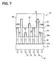
- opposing side walls 62a of the slit 62 prevent the joint portion 70b from being displaced in the length direction of the housing 60. Accordingly, a rotational movement of the terminal 70 around the first parallel portion 70a is prevented. The rotational movement is indicated by a solid arrow in FIG. 7 . Therefore, the terminals 70 (i.e., the contact portions 70d) can be accurately positioned with respect to the lands 34-39 without using a tine plate.
- the first parallel portions 70a are located at different heights from the surface 31a of the wiring board 31.
- the joint portions 70b are located at different distances from the second side 60b of the housing 60.
- a distance between adjacent joint portions 70b is long compared to when the joint portions 70b are located at the same distance from the second side of the housing 60. Accordingly, crosstalk between adjacent terminals 70 is less likely to occur. Therefore, the number of the terminals 70 can be increased without increasing the size of the housing 60 in the length direction.
- the connector 50 can have a large number of the terminals 70 without increasing the size.
- the terminals 70 can be accurately positioned with respect to the lands 34-39 and reliably connected to the lands 34-39.
- the connector 50 is mounted on the circuit board 30 in such a manner that the contact portions 70d of the terminals 70 are located perpendicular to the surface 31 a of the wiring board 31, inserted in the through holes 33, and soldered to the lands 34-39 that are formed on the inner walls of the through holes 33 and around the openings of the through holes 33. That is, the connector 50 is configured as a through hole connector.
- the terminals 70 can be accurately positioned with respect to the lands 34-39 without using a tine plate. Further, the terminals 70 can be reliably connected to the lands 34-39 without increasing the size of the connector 50 in the direction perpendicular to the surface 31 a of the wiring board 31.
- the second parallel portion 70c of the second terminal 79, the second parallel portion 70c of the first terminal 78, the first parallel portion 70a of the second terminal 79, and the first parallel portion 70a of the first terminal 78 are arranged in this order from the surface 31 a side. That is, the second parallel portion 70c of the first terminal 78 is located closer to the surface 31 a than the first parallel portion 70a of the second terminal 79. In such an approach, the length of a portion (e.g., contact portion 70d) of the first terminal 78 located closer to the surface 31 a than the second parallel portion 70c can be reduced.
- the first parallel portion 70a of the first terminal 78 is located farther from the surface 31 a of the wiring board 31 than the first parallel portion 70a of the second terminal 79, the first terminal 78 can be accurately positioned with respect to the lands 35, 38, 39.
- the signal terminals 73-76 are identical in cross-section (i.e., diameter).
- the joint portions 70b of the signal terminals 73-76 are located at X different distances from the second side 60b of the housing 60, where X is two. Specifically, each of the joint portions 73b, 74b is located at the third distance from the second side 60b, and each of the joint portions 75b, 76b is located at the fourth distance greater than the fourth distance.
- the first parallel portions 70a of the signal terminals 73-76 are located at Y different heights from the surface 31 a of the wiring board 31, where Y is four.
- the first parallel portion 73a is located at the third height from the surface 31 a
- the first parallel portion 74a is located at the fourth height greater than the third height
- the first parallel portion 75a is located at the fifth height greater than fourth height
- the first parallel portion 76a is located at the sixth height greater than the fifth height.
- the different distance step X (two) of the joint portions 70b is less than the different height step Y (four) of the first parallel portions 70a (i.e., 2 ⁇ X ⁇ Y).
- the terminal 70 has the second parallel portion 70c extending in the width direction of the housing 60, the increase in the size of the connector 50 in the width direction can be prevented.
- the different height step Y of the first parallel portions 70a is a multiple of the different distance step X of the joint portions 70b. Therefore, the connector 50 can have a large number of terminals 70 while preventing crosstalk between the adjacent terminals 70.
- the contact portions 70d of the signal terminals 73-76 are located at Z different distances from the second side 60b of the housing 60, where Z is four. Specifically, the contact portion 74d is located closer to the second side 61 b than the contact portion 73d, the contact portion 74d is located closer to the second side 61 b than the contact portion 76d, and the contact portion 76d is located closer to the second side 61 b than the contact portion 75d.
- the different distance step X (two) of the joint portions 70b is less than the different distance step Z (four) of the contact portions 70d (i.e., 2 ⁇ X ⁇ Z).
- the terminal 70 has the second parallel portion 70c extending in the width direction of the housing 60, the increase in the size of the connector 50 in the width direction can be prevented.
- the distance between adjacent terminals 70 can be increased by increasing the different distance step Z. Accordingly, the crosstalk between adjacent terminals can be reduced.
- the widths of the lands 36-39 can be increased by increasing the different distance step Z to improve the connection reliability between the terminals 73-76 and the lands 36-39.
- the above-described requirements can be applied to terminals 70 other than the signals terminals 73-76, as long as the terminals 70 are identical in cross-section.
- the above-described requirements can be applied to the power terminals 71, 72.
- the contact portions 70d of the terminals 70 having the same diameter are arrange in a zigzag manner.
- the crosstalk between adjacent terminals 70 can be reduced.
- the widths of the lands 34-39 can be increased so that the connection reliability between the terminals 70 and the lands 34-39 can be improved.
- the size of the wiring board 31 in the length direction can be reduced.
- the terminals 70 are classified into the first and second terminals 78, 79 according to the distance of the joint portion 70b from the second side 60b of the housing 60.
- the power terminal 72 and the signal terminals 75, 76 are classified as the first terminal 78, and the power terminal 71 and the signal terminals 73, 74 are classified as the second terminal 79.
- the terminal 70 having the first parallel portion 70a located father from the surface 31 a of the wiring board 31 has the contact portion 70d located closer to the second side 60b of the housing 60.
- each first terminal 78 having the same diameter has substantially the same length
- the second terminals 79 having the same diameter has substantially the same length.
- the signal terminals 75, 76 as the first terminal 78 has substantially the same length. Accordingly, each first terminals 78 has substantially the same impedance, and each second terminal 79 has substantially the same impedance. Therefore, a local increase of temperature in the terminals 70 can be reduced.
- the joint portion 70b of the first terminal 78 and the joint portion 70b of the second terminal 79 are arranged in the length direction of the housing 60 to form a zigzag arrangement.
- a distance L (refer to FIG. 9 ) between adjacent terminals 70 can be increased so that the crosstalk between the adjacent terminals 70 can be reduced.
- the zigzag arrangement can allow a visual inspection for a solder joint between the contact portion 70d located closer to the housing 60 and the corresponding land to be easily performed.
- the terminals 70 have two types of power terminals 71, 72 and four types of signal terminals 73-76, the number of types of the terminals 70 can vary according to the intended use of the connector 50.
- the terminals 70 can have one type of the terminals 70 having the same diameter or more than three types of the terminals 70 having the same diameter.
- the different distance step X of the joint portions 70b, the different height step Y of the first parallel portions 70a, and the different distance step Z of the contact portions 70d can vary according to the intended use, as long as each of the different distance step X and the different height step Y is two or more.
- the electronic control apparatus 1 is not made waterproof.
- the electronic control apparatus 1 can be made waterproof.
- the joint portion 70b is placed in the slit 62 not to be exposed to the plane formed by the first side 60a.
- the joint portion 70b can be placed in the slit 62 to be exposed to the plane formed by the first side 60a.
- the first end of the joint portion 70b is joined to the second end of the first parallel portion 70a and supported by the housing 60.
- the joint portion 70b is supported by the housing 60 at a joint between the first parallel portion 70a and the joint portion 70b.
- the joint portion 70b can be supported by the housing 60 at a portion other than the joint between the first parallel portion 70a and the joint portion 70b.
- the joint portion 70b can be supported by the housing 60 at a portion located away from the joint between the first parallel portion 70a and the joint portion 70b. In such an approach, the joint between the first parallel portion 70a and the joint portion 70b are exposed outside the housing. Therefore, the terminals 70 can be easily inserted in the housing 60.
- the contact portion 70d has an insertion portion that is inserted into the through hole 33 of the wiring board 31 and soldered to the corresponding land in the through hole 33 using a point soldering method.
- the contact portion 70d can have both the insertion portion and a surface-mount portion that is soldered to the corresponding land on the surface 31 a using a reflow soldering method.
- the contact portions 70d can have only the surface-mount portion.
- the contact portions 70d having the surface-mount structure can be mounted on the wiring board by a reflow soldering method.
- a reflow soldering method When the second parallel portion 70c of the first terminal 78 is located closer to the surface 31 a of the wiring board 31 than the first parallel portion 70a of the second terminal 79, reflow heat is effectively supplied to the contact portion 70d of the second terminal 79 without being blocked by the first terminal 78, so that the connection reliability between the terminal 79 and the corresponding land can be increased. Therefore, as shown in FIG.
- the second parallel portion 70c of the second terminal 79, the second parallel portion 70c of the first terminal 78, the first parallel portion 70a of the second terminal 79, and the first parallel portion 70a of the first terminal 78 be arranged in this order from the surface 31 a side. Further, in the terminals 70 having the same diameter, it is preferable that the first joint portion 70b of the first terminal 78 and the first joint portion 70b of the second terminal 79 are arranged in the length direction of the housing 60 to form a zigzag arrangement.
- the reflow heat is effectively supplied to the contact portion 70d of the second terminal 79 without being blocked by the joint portion 70b of the first terminal 78, so that the connection reliability between the terminal 79 and the lands can be increased.
- the zigzag arrangement can reduce the crosstalk between adjacent terminals 70 and can allow a visual inspection for the solder joint between the contact portion 70d of the second terminal 79 and the corresponding land to be easily performed.
- the contact portion 70d has both an insertion portion 70e and a surface-mount portion 70f.
- the surface-mount portion 70f extends substantially parallel to the surface 31 a of the wiring board 31 in the width direction of the housing 60.
- the insertion portion 70e extends perpendicular to the surface 31 a of the wiring board 31 from a tip of the surface-mount portion 70f and inserted in the through hole 33 of the wiring board 31.
- the terminal 70 can be a stamped terminal that is formed by stamping a sheet metal into a shape corresponding to the terminal 70.
- the terminal 70 can be formed by stamping a sheet metal into a straight shape and then by bending the straight-shaped sheet metal into the corresponding shape.
- the insertion portion 70e can extend perpendicular to the surface 31 a of the wiring board 31 from a potion other than the tip of the surface-mount portion 70f.
- the insertion portion 70e can extend perpendicular to the surface 31 a of the wiring board 31 from a middle potion of the surface-mount portion 70f.
- the terminal 70 includes six types of signal terminals.
- the first parallel portions 70a of the signal terminals are located at six different heights from the surface 31a of the wiring board 31. That is, the first parallel portions 70a of the signal terminals are located at different heights, respectively.
- the joint portions 70b of the signal terminals are located at three different distances from the second side 60b of the housing 60 in the width direction of the housing 60. Specifically, the joint portions 70b of the upper two signal terminals are located at the same distance from the second side 60b, the joint portions 70b of the middle two signal terminals are located at the same distance from the second side 60b, and the joint portions 70b of the lower two signal terminals are located at the same distance from the second side 60b.
- the signal terminals are classified into first, second, and third terminals 80-82 according to the distance of the joint portion 70b from the second side 60b.
- Each first parallel portion 70a of the first terminal 80 is located farther from the surface 31 a than each first parallel portions 70a of the second terminal 81.
- Each first parallel portion 70a of the second terminal 81 is located farther from the surface 31 a than each first parallel portions 70a of the third terminal 82.
- Each joint portion 70b of the third terminal 82 has a straight portion and a C-shaped portion. The straight portion is joined to the first parallel portion 70a, supported by the housing 60, and extends perpendicular to the surface 31a.
- the C-shaped portion is exposed outside the housing 60, located closer to the second side 60b of the housing 60 than the straight portion, and joined between the straight portion and the second parallel portion 70c.
- the length of the third terminal 82 is increased so that the connection reliability between the third terminal 82 and lands 40 can be improved.
- a vertex 70g of the C-shaped portion is thinned. The thinned vertex 70g reduces stress applied to the solder joint between the third terminal 70 and the land 40 so that the connection reliability between the third terminal 70 and the land 40 can be improved. Since only the vertex 70g is thinned, an increase in impedance of the third terminal 82 is kept as low as possible.
- the first and second terminals can have the C-shaped portion, for example, between the first joint portion 70b and the second parallel portion 70c.
- the joint portions 70b are arranged in the width direction of the housing 60 to from a zigzag arrangement.
- the joint portions 70b can be arranged in a manner other than a zigzag manner.
- the joint portions 70b can be arranged in a grid manner.
- the through hole 33 can be replaced with a blind hole that is not exposed to a back surface, opposite to the surface 31 a, of the wiring board 31.
Landscapes
- Coupling Device And Connection With Printed Circuit (AREA)
- Multi-Conductor Connections (AREA)
Abstract
Description
- The present invention relates to a connector adapted to be mounted on a wiring board and also relates to an electronic control apparatus having the connector and the wiring board.
- As disclosed in, for example,
JP-A-2000-164273 JP-A-2007-179974 - In the through-hole connector disclosed in
JP-A-2000-164273 - In such a through-hole connector with a tine plate, when the length of the terminal between a first portion supported by the tine plate and a second portion soldered to the land of the wiring board is short, the terminal is subjected to a lot of stress. Since the stress can cause disconnection between the terminal and the land, there is a need to increase the length of the terminal between the first and second portions. That is, the length of the terminal between the tine plate and the wiring board needs to be increased to reduce the stress applied to the terminal. As a result, the distance between the tine plate and the wiring board is increased. Accordingly, the size of the connector in a direction perpendicular to the surface of the wiring board is increased.
- In the surface-mount connector disclosed in
JP-A-2007-179974 - In view of the above, it is an object of the present invention to provide a connector configured such that even when the connector has a large number of terminals, the terminals can be accurately positioned with respect to lands of a wiring board, and a crosstalk between adjacent terminals can be reduced. It is another object of the present invention to provide an electronic control apparatus having the connector and the wiring board.
- According to an aspect of the present invention, a connector includes a housing and multiple terminals arranged in the housing in a length direction of the housing. The housing of the connector has an electrically insulating property and is adapted to be mounted on a surface of a wiring board having multiple lands. The housing has first and second sides opposite to each other in a width direction of the housing. Each terminal of the connector is exposed to the first side of the housing at one end to be electrically connected to the wiring board and exposed to the second side of the housing at the other end to be electrically connected to an external connector. Each terminal includes a first parallel portion, a joint portion, a second parallel portion, and a contact portion. The first parallel portion is partially supported by the housing and extends substantially parallel to the surface of the wiring board. The second parallel portion is exposed outside the housing and extends substantially parallel to the surface of the wiring board. The second parallel portion is located closer to the surface of the wiring board than the first parallel portion in a direction perpendicular to the surface of the wiring board. The joint portion extends substantially perpendicular to the surface of the wiring board. The joint portion has a first end joined to the first parallel portion and a second end exposed outside the housing and joined to a first end of the second parallel portion. A contact portion has a first end joined to a second end of the second parallel portion and a second end soldered to a corresponding land of the wiring board. The first parallel portions of the terminals are located at X different heights from the surface of the wiring board in a direction perpendicular to the surface of the wiring board, where X is an integer of two or more. The joint portions of the terminals are located at Y different distances from the second side of the housing in the width direction of the housing, where Y is an integer of two or more. A first one of the terminals has the first parallel portion located at a first height from the surface of the wiring board and has the joint portion located at a first distance from the second side of the housing. A second one of the terminals has the first parallel portion located at a second height, less than the first height, from the surface of the wiring board and has the joint portion located at a second distance, different than the first distance, from the second side of the housing. The joint portion of the first one of the terminals is supported by the housing at a position between the first parallel portion of the first one of the terminals and the first parallel portion of the second one of the terminals.
- According to another aspect of the present invention, an electronic control apparatus includes the connector and a wiring board having multiple lands. The housing of the connector is placed on the surface of the wiring board. The contact portion of each terminal is soldered to a corresponding land.
- The above and other objectives, features and advantages of the present invention will become more apparent from the following detailed description made with check to the accompanying drawings. In the drawings:
-
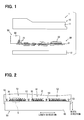
FIG. 1 is a diagram illustrating an exploded view of an electronic control apparatus according to an embodiment of the present invention; -
FIG. 2 is a diagram illustrating a top view of a connector mounted on a wiring board of the electronic control apparatus; -
FIG. 3 is a diagram illustrating a first side view of the connector mounted on the wiring board of the electronic apparatus; -
FIG. 4 is a diagram illustrating a second side view of the connector mounted on the wiring board of the electronic apparatus; -
FIG. 5 is a diagram illustrating an enlarged view of a portion enclosed by a line V ofFIG. 2 ; -
FIG. 6 is a diagram illustrating a cross-sectional view taken along line VI-VI ofFIG. 4 ; -
FIG. 7 is a diagram illustrating an enlarged view of a portion enclosed by a line VII ofFIG. 3 ; -
FIG. 8 is a diagram illustrating a cross-sectional view taken along line VIII-VIII ofFIG. 7 ; -
FIG. 9 is a diagram illustrating a cross-sectional view taken along line IX-IX ofFIG. 7 ; -
FIG. 10 is a diagram illustrating a cross-sectional view of an electronic control apparatus according to a modification of the embodiment; and -
FIG. 11 is a diagram illustrating a cross-sectional view of an electronic control apparatus according to another modification of the embodiment. - An
electronic control apparatus 1 according to an embodiment of the present invention is described below with reference toFIGS. 1-9 . For example, theelectronic control apparatus 1 can be applied to an engine electronic control unit (ECU) of a vehicle. In the embodiment, theelectronic control apparatus 1 has a non-waterproof structure. - As shown in
FIG. 1 , theelectronic control apparatus 1 mainly includes acircuit board 30 and aconnector 50. Thecircuit board 30 includes awiring board 31 andelectronic devices 32 mounted on thewiring board 31. Theconnector 50 includes aconnector housing 60 andconnector terminals 70 supported by thehousing 60. In the embodiment, theelectronic control apparatus 1 further includes acasing 10 for accommodating thecircuit board 30 and theconnector 50. - The
casing 10 can be, for example, made of a resin material or a metal material such as iron. Thecasing 10 can be constructed of one piece or separate pieces assembled together. In the embodiment, as shown inFIG. 1 , thecasing 10 includes acase 11 shaped like a box with an opening and a substantiallyrectangular lid 12 that covers the opening of thecase 11. Thecase 11 has a connector opening (not shown) shaped to match thehousing 60. In a condition where thelid 12 is attached to thecase 11, for example, by a screw, while thecircuit board 30 is entirely accommodated in thecasing 10, theconnector 50 is partially exposed outside thecasing 10 through the connector opening. - As mentioned above, the
circuit board 30 includes thewiring board 31 and theelectronic devices 32 mounted on thewiring board 31. Thewiring board 31 has wiring patterns (not shown) joined to theelectronic devices 32 and via holes (not shown) connecting the wiring patters. Examples of theelectronic devices 32 include microcomputers (i.e., microprocessors), power transistors, resistors, and capacitors. Theconnector 50 is also mounted on thewiring board 31 and configured to electrically connect thecircuit board 30 to an external device. - As mentioned above, the
connector 50 includes thehousing 60 and theterminals 70 supported by thehousing 60. Thehousing 60 is made of an electrically insulating material such as resin. Thehousing 60 has a substantially rectangular prism shape with length and width directions as indicated inFIG. 2 . Theconnector terminals 70 are made of an electrically conductive material such as copper. As shown inFIG. 6 , eachconnector terminal 70 is exposed at one end to afirst side 60a of thehousing 60 and electrically coupled to thecircuit board 30, which is accommodated in thecasing 10. Eachconnector terminal 70 is exposed at the other end to asecond side 60b of thehousing 60 and located outside thecasing 10 to be electrically connected to an external connector (not shown). - The
connector terminal 70 can be a stamped terminal that is formed by stamping a sheet metal into a predetermined shape. Alternatively, theconnector terminal 70 can be a bent terminal that is formed by stamping a metal sheet into a straight shape, inserting the straight-shaped terminal into thehousing 60, and then bending the straight-shaped terminal into the predetermined shape. Theconnector terminal 70 can have an accurate shape, when theconnector terminal 70 is a stamped terminal as compared to when theconnector terminal 70 is a bent terminal. Theconnector terminal 70 can be brass plated. - As shown in
FIGS. 2-4 , theconnector terminals 70 are supported by thehousing 60 and arranged in the length direction of thehousing 60 so as not to interfere with each other. In the embodiment, theconnector terminals 70 includepower terminals power terminals power terminals power terminals power terminals - As shown in
FIGS. 5 ,6 , thewiring board 31 has throughholes 33 and conductive lands 34-39. The lands 34-39 are integrally formed on inner walls of the throughholes 33 and around openings of the throughholes 33, respectively. The through holes 33 penetrate through thewiring board 31 in a direction perpendicular to asurface 31 a of thewiring board 31. - The lands 34-39 correspond to the terminals 71-76, respectively. That is, the terminals 71-76 are inserted into the through
holes 33 and electrically joined to the lands 34-39 throughsolders 90, respectively. The shape and size of the throughholes 33 are adjusted to match the terminals 71-76. For example, since thepower terminals holes 33 for receiving thepower terminals holes 33 for receiving the signal terminals 73-76. - The
lands 34 for thepower terminals 71 are arranged in a line in the length direction of thehousing 60. Thelands 35 for thepower terminals 72 are arranged in a line in the length direction of thehousing 60. Theland 35 is located farther from thesecond side 60b of thehousing 60 than theland 34 in the width direction of thehousing 60. Thelands housing 60 to form a two-legged zigzag arrangement. - The
lands 36 for thesignal terminals 73 are arranged in a line in the length direction of thehousing 60. Thelands 37 for thesignal terminals 74 are arranged in a line in the length direction of thehousing 60. Thelands 38 for thesignal terminals 75 are arranged in a line in the length direction of thehousing 60. Thelands 39 for thesignal terminals 76 are arranged in a line in the length direction of thehousing 60. Theland 37 is located farther from thesecond side 60b of thehousing 60 than theland 36 in the width direction of thehousing 60. Theland 38 is located farther from thesecond side 60b than theland 37. Theland 39 is located farther from thesecond side 60b than theland 38. Thelands housing 60 so as to provide a four-legged zigzag arrangement. - Each
connector terminal 70 has a firstparallel portion 70a, a firstjoint portion 70b, a secondparallel portion 70c, and acontact portion 70d. For example, as shown inFIG. 6 , the signal terminals 73-76 have first parallel portions 73a-76a, firstjoint portions 73b-76b, second parallel portions 73c-76c, andcontact portions 73d-76d, respectively. Although not shown in the drawings, thepower terminals contact portions - The first
parallel portion 70a of theconnector terminal 70 extends substantially parallel to thesurface 31 a of thewiring board 31 in the width direction of thehousing 60. The firstparallel portion 70a has a first end that projects from thesecond side 60b of thehousing 60 to be electrically connected to the external connector. A second end of the firstparallel portion 70a is supported by thehousing 60. - Specifically, as exemplified in
FIG. 6 by the firstparallel portions signal terminals parallel portion 70a is placed in a throughhole 61 and aslit 62 formed in thehousing 60. The throughhole 61 penetrates through thehousing 60 in the width direction of thehousing 60. Theslit 62 is formed on thefirst side 60a and extends in the direction perpendicular to thesurface 31 a of thewiring board 31. The upper end of theslit 62 communicates with the throughhole 61. In the embodiment, the firstparallel portion 70a is inserted in the throughhole 61 and theslit 62 from thefirst side 60a of thehousing 60. - A
projection 77 is formed on an outer surface of the second end of the firstparallel portion 70a, and arecess 61 a is formed on an inner wall of the throughhole 61. When the firstparallel portion 70a is inserted in the throughhole 61, theprojection 77 of the firstparallel portion 70a is received in (i.e., engaged with) therecess 61 a of the throughhole 61 to prevent the firstparallel portion 70a from moving toward thefirst side 60a of thehousing 60. Further, thejoint portion 70b and a bottom 62b (refer toFIG. 8 ) of theslit 62 prevents the firstparallel portion 70a from moving toward thesecond side 60b of thehousing 60. Thus, the terminal 70 remains supported by thehousing 60. - As shown in, for example,
FIGS. 3, 4 , the first parallel portions 71 a, 72a of thepower terminals surface 31 a of thewiring board 31 in the direction perpendicular to thesurface 31 a. Further, the first parallel portions 71 a, 72a are alternately arranged in the length direction of thehousing 60 to form a two-legged zigzag arrangement. Specifically, the first parallel portion 71 a is located at a first height from thesurface 31 a, and the first parallel portion 72a is located at a second height greater than the first height. - As shown in, for example,
FIG. 6 , the first parallel portions 73a-76a of the signal terminals 73-76 are located at four different heights from thesurface 31a of thewiring board 31 in the direction perpendicular to thesurface 31a. Specifically, the first parallel portion 73a is located at a third height from thesurface 31 a, the firstparallel portion 74a is located at a fourth height greater than the third height, the first parallel portion 75a is located at a fifth height greater than fourth height, and the firstparallel portion 76a is located at a sixth height greater than the fifth height. Further, the firstparallel portions housing 60 to form a four-legged zigzag arrangement. - As exemplified in
FIG. 6 by the secondparallel portions signal terminals parallel portion 70c is located closer to thesurface 31 a of thewiring board 31 than the firstparallel portion 70a and extends substantially parallel to thesurface 31 a in the width direction of thehousing 60. The secondparallel portion 70c is entirely exposed outside thehousing 60 on thefirst side 60a side. The secondparallel portion 70c has a first end joined to the second end of thejoint portion 70b and a second end joined to a first end of thecontact portion 70d. That is, the first and secondparallel portions joint potion 70b. - As exemplified in
FIG. 6 by thejoint portions signal terminals joint portion 70b extends substantially perpendicular to thesurface 31 a of thewiring board 31. Thejoint portion 70b has a first end joined to the second end of the firstparallel portion 70a and a second end projecting from thefirst side 60a of thehousing 60 toward thesurface 31 a of thewiring board 31. Thejoint portion 70b is partially supported by thehousing 60 in such a manner that the second end of thejoint portion 70b is exposed outside thehousing 60. In the embodiment, as shown in, for example,FIGS. 6-9 , the first end of thejoint portion 70b is placed in theslit 62 and thus supported by thehousing 60. As clearly illustrated inFIG. 8 , thejoint portion 70b placed in theslit 62 does not touch a plane formed by thefirst side 60a. In such an approach, a foreign matter sticking to thefirst side 60a cannot touch thejoint portion 70b. Therefore, even when the foreign matter has an electrical conductivity, the foreign matter does not cause a short-circuit between adjacentjoint portions 70b. - The joint portions 71 b, 72b of the
power terminals second side 60b of thehousing 60 in the width direction of thehousing 60. Specifically, the joint portion 72b is located at a first distance from thesecond side 60b, and the joint portion 71 b is located at a second distance greater than the first distance. - The
joint portions signal terminals second side 60b of thehousing 60 in the width direction of thehousing 60. Thejoint portions signal terminals second side 60b of thehousing 60 in the width direction of thehousing 60. Specifically, each of thejoint portions second side 60b, and each of thejoint portions joint portions 73b-76b of the signal terminals 73-76 are located at two different distances from thesecond side 60b of thehousing 60 in the width direction of thehousing 60. - In the embodiment, the
terminals 70 having the same diameter are classified into first andsecond terminals joint portion 70b from thesecond side 60b of thehousing 60. For example, thepower terminal 72 and thesignal terminals first terminal 78, and thepower terminal 71 and thesignal terminals second terminal 79. Thejoint portion 70b of thefirst terminal 78 is supported by thehousing 60 at a position between the firstparallel portions 70a of the first andsecond terminals - Specifically, the joint portion 72b of the
power terminal 72 as thefirst terminal 78 is supported by thehousing 60 at a position between the first parallel portion 72a of thepower terminal 72 and the first parallel portion 71 a of thepower terminal 71 as thesecond terminal 79. Thejoint portion 75b of thesignal terminal 75 as thefirst terminal 78 is supported by thehousing 60 at a position between the first parallel portion 75a of thesignal terminal 75 and the first parallel portion 73a of thesignal terminal 73 as thesecond terminal 79. Thejoint portion 76b of thesignal terminal 76 as thefirst terminal 78 is supported by thehousing 60 at a position between the firstparallel portion 76a of thesignal terminal 76 and the firstparallel portion 74a of thesignal terminal 74 as thesecond terminal 79. - As shown, for example, in
FIG. 6 , in the first andsecond terminals parallel portion 70c of thesecond terminal 79, the secondparallel portion 70c of thefirst terminal 78, the firstparallel portion 70a of thesecond terminal 79, and the firstparallel portion 70a of thefirst terminal 78 are arranged in this order from thesurface 31 a side. - As shown, for example, in
FIG. 9 , thejoint portion 70b of the first terminal 78 (i.e., thejoint portions signal terminals 75, 76) and thejoint portion 70b of the second terminal 79 (i.e., thejoint portions signal terminals 73, 74) are alternately arranged in the length direction of thehousing 60 to form a two-legged zigzag arrangement. - The
contact portion 70d of the terminal 70 is electrically joined to a corresponding one of the lands 34-39 of thewiring board 31. In the embodiment, thewiring board 31 has throughholes 33. The lands 34-39 are integrally formed on inner walls of the throughholes 33 and formed around openings of the through holes 33. As shown inFIGS. 5 and6 , thecontact portions 70d are inserted into throughholes 33 and electrically joined to the lands 34-39 throughsolders 90. - As shown in
FIG. 5 , thecontact portions 71 d of thepower terminals 71 are arranged in a line in the length direction of thehousing 60. Likewise, thecontact portions 72d of thepower terminals 72 are arranged in a line in the length direction of thehousing 60. Thecontact portion 71d of thepower terminal 71 as thefirst terminal 78 is located closer to the second side 61 b of thehousing 60 than thecontact portion 72d of thepower terminal 72 as thefirst terminal 78. Thecontact portions lands housing 60 to form a two-legged zigzag arrangement. - As shown in
FIG 5 , thecontact portions 73d of thesignal terminals 73 are arranged in a line in the length direction of thehousing 60. Likewise, thecontact portions 74d of thesignal terminals 74 are arranged in a line in the length direction of thehousing 60. Likewise, thecontact portions 75d of thesignal terminals 75 are arranged in a line in the length direction of thehousing 60. Likewise, thecontact portions 76d of thesignal terminals 76 are arranged in a line in the length direction of thehousing 60. Thecontact portion 74d of thesignal terminal 74 as thesecond terminal 79 is located closer to the second side 61 b of thehousing 60 than thecontact portion 73d of thesignal terminal 73 as thesecond terminal 79. Thecontact portion 74d of thesignal terminal 74 as thesecond terminal 79 is located closer to the second side 61 b of thehousing 60 than thecontact portion 76d of thesignal terminal 76 as thefirst terminal 78. Thecontact portion 76d of thesignal terminal 76 as thefirst terminal 78 is located closer to the second side 61 b of thehousing 60 than thecontact portion 75d of thesignal terminal 75 as thefirst terminal 78. Thecontact portions 73d-76d are soldered to the lands 36-39, respectively. Further, thecontact portions housing 60 to form a four-legged zigzag arrangement. - Further, as shown in
FIG. 6 , thecontact portion 70d has a cross-section (i.e., diameter) smaller than that of any other portion of the terminal 70 exposed outsidehousing 60 on thefirst side 60a side. Specifically, thecontact portion 70d has a cross-section smaller than that of each of the second end of thejoint portion 70b and the secondparallel portion 70c. In such an approach, the size of the throughhole 33 is reduced so that the area of thewiring board 31 occupied by the thoughhole 33 can be reduced. Since each of thejoint portion 70b and the secondparallel portion 70c has a large cross section enough to reduce impedance of the terminal 70, heat generated in the terminal 70 is reduced. Further, the large cross section of thejoint portion 70b and the secondparallel portion 70c increases strength of the terminal 70 so that a bend of the terminal 70 can be reduced. Therefore, thecontact portions 70d can be inserted in the throughholes 33 while positioning theterminals 70 with respect to the through holes 33. - As shown in
FIGS. 2-4 , theconnector 50 has onefirst terminal block 51 and twosecond terminal block 52 that are arranged in a line in the length direction of thehousing 60. The firstterminal block 51 is constructed with only the signal terminals 73-76. Each secondterminal block 52 is constricted with both thepower terminals FIG. 4 , the first and second terminal blocks 51-52 are separated from each other by thesecond side 60b of thehousing 60. In such an approach, thehousing 60 can be prevented from warping in the length direction. The arrangement of the terminal blocks and the arrangement of the terminals in the terminal block can vary according to the intended use, for example, as disclosed in Japanese Patent Application No.20007-000888 - In the embodiment, as shown in
FIGS. 2 ,3 , thehousing 60 is fixed to thewiring board 31 by fourreinforcement pins 53 that are arranged in a line in the length direction of thehousing 60 at a given interval. In such an approach, theconnector 50 can be reliably fixed to thewiring board 31. The number and arrangement of the reinforcement pins 53 can vary according to the intended use. Alternatively, the reinforcement pins 53 can be unnecessary, because theconnector 50 can be securely fixed to thewiring board 31 by thecontact portions 70d, which are inserted in the throughholes 33 and soldered to the lands 34-39 of thewiring board 31. - In summary, the following advantages can be achieved according to the embodiment. The first end of the
joint portion 70b is joined to the firstparallel portion 70a, and the second end of thejoint portion 70b is joined to the secondparallel portion 70c. As shown inFIG. 6 , the first end of thejoint portion 70b is supported by thehousing 60, and the second end of thejoint portion 70b is exposed outside thehousing 60. That is, the secondparallel portion 70c and the second end of thejoint portion 70b are located between thecontact portion 70d and the first end of thejoint portion 70b. In such an approach, the length of the terminal 70 between thefirst side 60a of thehousing 60 and thesurface 31a of thewiring board 31 becomes long enough to reduce stress applied to the terminal 70. Thus, connection reliability between theterminals 70 and the lands 34-39 can be ensured without increasing the size of theconnector 50 in the direction perpendicular to thesurface 31 a of thewiring board 31. - In particular, in the embodiment, the
joint portion 70b of thefirst terminal 78 is supported by thehousing 60 at a position between the firstparallel portion 70a of thefirst terminal 78 and the firstparallel portion 70a of thesecond terminal 79. That is, thejoint portion 70b of thefirst terminal 78 is supported by thehousing 60 at a position relatively far away from thesurface 31 a of thewiring board 31 in the direction perpendicular to thesurface 31a. Therefore, the connection reliability can be effectively increased. - Further, in the embodiment, the first end of the
joint portion 70b of the terminal 70 is covered with thehousing 60. For example, the length of the first end of thejoint portion 70b can account for from about one-third to two-thirds of the total length of thejoint portion 70b. In such an approach, thejoint portion 70b is supported by thehousing 60 at a position relatively far away from thesurface 31 a of thewiring board 31 in the direction perpendicular to thesurface 31 a. Thus, the connection reliability between theterminals 70 and the lands 34-39 can be increased without increasing the size of theconnector 50 in the direction perpendicular to thesurface 31 a. Since a top side (i.e., the first end) of thejoint portion 70b is supported by thehousing 60, thehousing 60 can be simplified in structure as compared to when a bottom side (i.e., the second end) of thejoint portion 70b is supported by thehousing 60. Further, since thejoint portion 70b is supported by a surface of thehousing 60, not a point of thehousing 60, theterminals 70 can be accurately positioned with respect to the lands 34-39. - Specifically, as shown in
FIGS. 6 ,7 , thehousing 60 has athick portion 63 and athin portion 64. The thickness of thethick portion 63 in the width direction of thehousing 60 is greater than the thickness of thethin portion 64. The firstparallel portion 70a and the first end of thejoint portion 70b of the first terminal 78 (i.e., thepower terminal 72 and thesignal terminals 75, 76) are supported by thethick portion 63. The firstparallel portion 70a and the first end of thejoint portion 70b of the second terminal 79 (i.e., thepower terminal 71 and thesignal terminals 73, 74) are supported by thethin portion 64. Due to the thickness difference between thethick portion 63 and thethin portion 64, thehousing 60 has a stepped shape at thefirst side 60a. The second end of thejoint portion 70b of the first terminal 78 projects from a bottom 63a of thethick portion 63 and is located in front of thefirst side 60a of thethin portion 64 with a space therebetween. The second end of thejoint portion 70b of the second terminal 79 projects from a bottom 64a of thethin portion 64 and is located in front of thefirst side 60a of a furtherthin portion 65 with a space therebetween. The thickness of the furtherthin portion 65 in the width direction of thehousing 60 is smaller than the thickness of thethin portion 64. In this way, the top side (i.e., the first end) of thejoint portion 70b of each terminal 70 is supported by thehousing 60. - As shown in
FIGS. 6-9 , the first end of thejoint portion 70b is placed in theslit 62 formed on thefirst side 60a of thehousing 60. For example, as shown inFIG. 8 , opposingside walls 62a of theslit 62 prevent thejoint portion 70b from being displaced in the length direction of thehousing 60. Accordingly, a rotational movement of the terminal 70 around the firstparallel portion 70a is prevented. The rotational movement is indicated by a solid arrow inFIG. 7 . Therefore, the terminals 70 (i.e., thecontact portions 70d) can be accurately positioned with respect to the lands 34-39 without using a tine plate. - As shown, for example, in
FIG. 6 , the firstparallel portions 70a are located at different heights from thesurface 31a of thewiring board 31. Further, thejoint portions 70b are located at different distances from thesecond side 60b of thehousing 60. In this case, a distance between adjacentjoint portions 70b is long compared to when thejoint portions 70b are located at the same distance from the second side of thehousing 60. Accordingly, crosstalk betweenadjacent terminals 70 is less likely to occur. Therefore, the number of theterminals 70 can be increased without increasing the size of thehousing 60 in the length direction. - As describe above, according to the embodiment, the
connector 50 can have a large number of theterminals 70 without increasing the size. Theterminals 70 can be accurately positioned with respect to the lands 34-39 and reliably connected to the lands 34-39. Theconnector 50 is mounted on thecircuit board 30 in such a manner that thecontact portions 70d of theterminals 70 are located perpendicular to thesurface 31 a of thewiring board 31, inserted in the throughholes 33, and soldered to the lands 34-39 that are formed on the inner walls of the throughholes 33 and around the openings of the through holes 33. That is, theconnector 50 is configured as a through hole connector. Although theconnector 50 is configured as a through hole connector, theterminals 70 can be accurately positioned with respect to the lands 34-39 without using a tine plate. Further, theterminals 70 can be reliably connected to the lands 34-39 without increasing the size of theconnector 50 in the direction perpendicular to thesurface 31 a of thewiring board 31. - Further, according to the embodiment, as shown, for example, in
FIG. 6 , the secondparallel portion 70c of thesecond terminal 79, the secondparallel portion 70c of thefirst terminal 78, the firstparallel portion 70a of thesecond terminal 79, and the firstparallel portion 70a of thefirst terminal 78 are arranged in this order from thesurface 31 a side. That is, the secondparallel portion 70c of thefirst terminal 78 is located closer to thesurface 31 a than the firstparallel portion 70a of thesecond terminal 79. In such an approach, the length of a portion (e.g.,contact portion 70d) of thefirst terminal 78 located closer to thesurface 31 a than the secondparallel portion 70c can be reduced. Therefore, although the firstparallel portion 70a of thefirst terminal 78 is located farther from thesurface 31 a of thewiring board 31 than the firstparallel portion 70a of thesecond terminal 79, thefirst terminal 78 can be accurately positioned with respect to thelands - In the embodiment, the signal terminals 73-76 are identical in cross-section (i.e., diameter). The
joint portions 70b of the signal terminals 73-76 are located at X different distances from thesecond side 60b of thehousing 60, where X is two. Specifically, each of thejoint portions second side 60b, and each of thejoint portions parallel portions 70a of the signal terminals 73-76 are located at Y different heights from thesurface 31 a of thewiring board 31, where Y is four. Specifically, the first parallel portion 73a is located at the third height from thesurface 31 a, the firstparallel portion 74a is located at the fourth height greater than the third height, the first parallel portion 75a is located at the fifth height greater than fourth height, and the firstparallel portion 76a is located at the sixth height greater than the fifth height. - In summary, the different distance step X (two) of the
joint portions 70b is less than the different height step Y (four) of the firstparallel portions 70a (i.e., 2≤X<Y). In such an approach, although the terminal 70 has the secondparallel portion 70c extending in the width direction of thehousing 60, the increase in the size of theconnector 50 in the width direction can be prevented. In particular, in the embodiment, the different height step Y of the firstparallel portions 70a is a multiple of the different distance step X of thejoint portions 70b. Therefore, theconnector 50 can have a large number ofterminals 70 while preventing crosstalk between theadjacent terminals 70. Further, thecontact portions 70d of the signal terminals 73-76 are located at Z different distances from thesecond side 60b of thehousing 60, where Z is four. Specifically, thecontact portion 74d is located closer to the second side 61 b than thecontact portion 73d, thecontact portion 74d is located closer to the second side 61 b than thecontact portion 76d, and thecontact portion 76d is located closer to the second side 61 b than thecontact portion 75d. - In summary, the different distance step X (two) of the
joint portions 70b is less than the different distance step Z (four) of thecontact portions 70d (i.e., 2≤X<Z). In such an approach, although the terminal 70 has the secondparallel portion 70c extending in the width direction of thehousing 60, the increase in the size of theconnector 50 in the width direction can be prevented. The distance betweenadjacent terminals 70 can be increased by increasing the different distance step Z. Accordingly, the crosstalk between adjacent terminals can be reduced. Further, the widths of the lands 36-39 can be increased by increasing the different distance step Z to improve the connection reliability between the terminals 73-76 and the lands 36-39. The above-described requirements (e.g., 2≤X<Y, 2≤X<Z) can be applied toterminals 70 other than the signals terminals 73-76, as long as theterminals 70 are identical in cross-section. For example, the above-described requirements can be applied to thepower terminals - According to the embodiment, the
contact portions 70d of theterminals 70 having the same diameter are arrange in a zigzag manner. In such an approach, the crosstalk betweenadjacent terminals 70 can be reduced. Further, the widths of the lands 34-39 can be increased so that the connection reliability between theterminals 70 and the lands 34-39 can be improved. Furthermore, as compared to when the lands 34-39 are arranged in a line in the length direction of thehousing 60, the size of thewiring board 31 in the length direction can be reduced. - According to the embodiment, the
terminals 70 are classified into the first andsecond terminals joint portion 70b from thesecond side 60b of thehousing 60. Thepower terminal 72 and thesignal terminals first terminal 78, and thepower terminal 71 and thesignal terminals second terminal 79. In each of the first andsecond terminals parallel portion 70a located father from thesurface 31 a of thewiring board 31 has thecontact portion 70d located closer to thesecond side 60b of thehousing 60. In other words, in each of the first andsecond terminals parallel portion 70a located closer to thesurface 31 a has thecontact portion 70d located farther from thesecond side 60b. In such an approach, eachfirst terminal 78 having the same diameter has substantially the same length, and thesecond terminals 79 having the same diameter has substantially the same length. For example, in the example shown inFIG. 6 , thesignal terminals first terminal 78 has substantially the same length. Accordingly, eachfirst terminals 78 has substantially the same impedance, and eachsecond terminal 79 has substantially the same impedance. Therefore, a local increase of temperature in theterminals 70 can be reduced. - According to the embodiment, in the
terminals 70 having the same diameter, thejoint portion 70b of thefirst terminal 78 and thejoint portion 70b of thesecond terminal 79 are arranged in the length direction of thehousing 60 to form a zigzag arrangement. In such an approach, a distance L (refer toFIG. 9 ) betweenadjacent terminals 70 can be increased so that the crosstalk between theadjacent terminals 70 can be reduced. Further, as compared to a grid arrangement, the zigzag arrangement can allow a visual inspection for a solder joint between thecontact portion 70d located closer to thehousing 60 and the corresponding land to be easily performed. - The embodiment described above can be modified in various ways. For example, although the
terminals 70 have two types ofpower terminals terminals 70 can vary according to the intended use of theconnector 50. For example, theterminals 70 can have one type of theterminals 70 having the same diameter or more than three types of theterminals 70 having the same diameter. The different distance step X of thejoint portions 70b, the different height step Y of the firstparallel portions 70a, and the different distance step Z of thecontact portions 70d can vary according to the intended use, as long as each of the different distance step X and the different height step Y is two or more. - In the embodiment, the
electronic control apparatus 1 is not made waterproof. Alternatively, theelectronic control apparatus 1 can be made waterproof. - In the embodiment, as shown in
FIG. 9 , thejoint portion 70b is placed in theslit 62 not to be exposed to the plane formed by thefirst side 60a. Alternatively, as shown inFIG. 10 , thejoint portion 70b can be placed in theslit 62 to be exposed to the plane formed by thefirst side 60a. - In the embodiment, the first end of the
joint portion 70b is joined to the second end of the firstparallel portion 70a and supported by thehousing 60. In short, thejoint portion 70b is supported by thehousing 60 at a joint between the firstparallel portion 70a and thejoint portion 70b. Alternatively, thejoint portion 70b can be supported by thehousing 60 at a portion other than the joint between the firstparallel portion 70a and thejoint portion 70b. For example, as shown inFIG. 11 , thejoint portion 70b can be supported by thehousing 60 at a portion located away from the joint between the firstparallel portion 70a and thejoint portion 70b. In such an approach, the joint between the firstparallel portion 70a and thejoint portion 70b are exposed outside the housing. Therefore, theterminals 70 can be easily inserted in thehousing 60. - In the embodiment, the
contact portion 70d has an insertion portion that is inserted into the throughhole 33 of thewiring board 31 and soldered to the corresponding land in the throughhole 33 using a point soldering method. Alternatively, thecontact portion 70d can have both the insertion portion and a surface-mount portion that is soldered to the corresponding land on thesurface 31 a using a reflow soldering method. Alternatively, thecontact portions 70d can have only the surface-mount portion. - The
contact portions 70d having the surface-mount structure can be mounted on the wiring board by a reflow soldering method. When the secondparallel portion 70c of thefirst terminal 78 is located closer to thesurface 31 a of thewiring board 31 than the firstparallel portion 70a of thesecond terminal 79, reflow heat is effectively supplied to thecontact portion 70d of thesecond terminal 79 without being blocked by thefirst terminal 78, so that the connection reliability between the terminal 79 and the corresponding land can be increased. Therefore, as shown inFIG. 6 , it is preferable that the secondparallel portion 70c of thesecond terminal 79, the secondparallel portion 70c of thefirst terminal 78, the firstparallel portion 70a of thesecond terminal 79, and the firstparallel portion 70a of thefirst terminal 78 be arranged in this order from thesurface 31 a side. Further, in theterminals 70 having the same diameter, it is preferable that the firstjoint portion 70b of thefirst terminal 78 and the firstjoint portion 70b of thesecond terminal 79 are arranged in the length direction of thehousing 60 to form a zigzag arrangement. In such an approach, the reflow heat is effectively supplied to thecontact portion 70d of thesecond terminal 79 without being blocked by thejoint portion 70b of thefirst terminal 78, so that the connection reliability between the terminal 79 and the lands can be increased. Further, the zigzag arrangement can reduce the crosstalk betweenadjacent terminals 70 and can allow a visual inspection for the solder joint between thecontact portion 70d of thesecond terminal 79 and the corresponding land to be easily performed. - In the example shown in
FIG. 11 , thecontact portion 70d has both aninsertion portion 70e and a surface-mount portion 70f. The surface-mount portion 70f extends substantially parallel to thesurface 31 a of thewiring board 31 in the width direction of thehousing 60. Theinsertion portion 70e extends perpendicular to thesurface 31 a of thewiring board 31 from a tip of the surface-mount portion 70f and inserted in the throughhole 33 of thewiring board 31. - For example, the terminal 70 can be a stamped terminal that is formed by stamping a sheet metal into a shape corresponding to the terminal 70. Alternatively, the terminal 70 can be formed by stamping a sheet metal into a straight shape and then by bending the straight-shaped sheet metal into the corresponding shape. When the terminal 70 is the stamped terminal, design flexibility of the terminal 70 is improved so that the terminal 70 can have a complex shape. For example, the
insertion portion 70e can extend perpendicular to thesurface 31 a of thewiring board 31 from a potion other than the tip of the surface-mount portion 70f. Specifically, as disclosed in, for example, Japanese Patent Application No.2007-148613 insertion portion 70e can extend perpendicular to thesurface 31 a of thewiring board 31 from a middle potion of the surface-mount portion 70f. - Further, in the example shown in
FIG. 11 , the terminal 70 includes six types of signal terminals. The firstparallel portions 70a of the signal terminals are located at six different heights from thesurface 31a of thewiring board 31. That is, the firstparallel portions 70a of the signal terminals are located at different heights, respectively. Thejoint portions 70b of the signal terminals are located at three different distances from thesecond side 60b of thehousing 60 in the width direction of thehousing 60. Specifically, thejoint portions 70b of the upper two signal terminals are located at the same distance from thesecond side 60b, thejoint portions 70b of the middle two signal terminals are located at the same distance from thesecond side 60b, and thejoint portions 70b of the lower two signal terminals are located at the same distance from thesecond side 60b. - The signal terminals are classified into first, second, and third terminals 80-82 according to the distance of the
joint portion 70b from thesecond side 60b. Each firstparallel portion 70a of thefirst terminal 80 is located farther from thesurface 31 a than each firstparallel portions 70a of thesecond terminal 81. Each firstparallel portion 70a of thesecond terminal 81 is located farther from thesurface 31 a than each firstparallel portions 70a of thethird terminal 82. Eachjoint portion 70b of thethird terminal 82 has a straight portion and a C-shaped portion. The straight portion is joined to the firstparallel portion 70a, supported by thehousing 60, and extends perpendicular to thesurface 31a. The C-shaped portion is exposed outside thehousing 60, located closer to thesecond side 60b of thehousing 60 than the straight portion, and joined between the straight portion and the secondparallel portion 70c. In such an approach, the length of thethird terminal 82 is increased so that the connection reliability between thethird terminal 82 and lands 40 can be improved. Further, avertex 70g of the C-shaped portion is thinned. The thinnedvertex 70g reduces stress applied to the solder joint between thethird terminal 70 and theland 40 so that the connection reliability between thethird terminal 70 and theland 40 can be improved. Since only thevertex 70g is thinned, an increase in impedance of thethird terminal 82 is kept as low as possible. The first and second terminals can have the C-shaped portion, for example, between the firstjoint portion 70b and the secondparallel portion 70c. - In the embodiment, the
joint portions 70b are arranged in the width direction of thehousing 60 to from a zigzag arrangement. Alternatively, thejoint portions 70b can be arranged in a manner other than a zigzag manner. For example, thejoint portions 70b can be arranged in a grid manner. - The through
hole 33 can be replaced with a blind hole that is not exposed to a back surface, opposite to thesurface 31 a, of thewiring board 31. - Such changes and modifications are to be understood as being within the scope of the present invention as defined by the appended claims.
Claims (17)
- A connector comprising:a housing (60) having an electrically insulating property and adapted to be mounted on a surface (31a) of a wiring board (31) with a plurality of lands (34-39), the housing (60) having first and second sides (60a, 60b) opposite each other in a width direction thereof; anda plurality of terminals (70) arranged in the housing (60) in a length direction of the housing (60), each terminal being exposed to the first side (60a) of the housing (60) at one end to be electrically connected to the wiring board (31) and exposed to a second side (60b) of the housing (60) at an other end to be electrically connected to an external connector, each terminal comprising:wherein the first parallel portions (70a) of the plurality of terminals (70) are located at X different heights from the surface (31a) of the wiring board (31) in the direction perpendicular to the surface (31a) of the wiring board (31), where X is an integer of two or more,a first parallel portion (70a) partially supported by the housing (60) and substantially parallel to the surface (31a) of the wiring board (31);a second parallel portion (70c) exposed outside the housing (60) and substantially parallel to the surface (31a) of the wiring board (31), the second parallel portion (70c) being located closer to the surface (31a) of the wiring board (31) than the first parallel portion (70a) in a direction perpendicular to the surface (31a) of the wiring board (31);a joint portion (70b) substantially perpendicular to the surface (31a) of the wiring board (31), the joint portion (70b) having a first end joined to the first parallel portion (70a) and a second end exposed outside the housing (60) and joined to a first end of the second parallel portion (70c); anda contact portion (70d) having a first end joined to a second end of the second parallel portion (70c) and a second end soldered to a corresponding land (34-39) of the wiring board (31),
wherein the joint portions (70b) of the plurality of terminals (70) are located at Y different distances from the second side (60b) of the housing (60) in the width direction of the housing (60), where Y is an integer of two or more,
wherein a first one (78) of the plurality of terminals (70) has the first parallel portion (70a) located at a first height from the surface (31 a) of the wiring board (31) and the joint portion (70b) located at a first distance from the second side (60b) of the housing (60),
wherein a second one (79) of the plurality of terminals (70) has the first parallel portion (70a) located at a second height, less than the first height, from the surface (31 a) of the wiring board (31) and the joint portion (70b) located at a second distance, different than the first distance, from the second side (60b) of the housing (60), and
wherein the joint portion (70b) of the first one (78) of the plurality of terminals (70) is supported by the housing (60) at a position between the first parallel portion (70a) of the first one (78) of the plurality of terminals (70) and the first parallel portion (70a) of the second one (79) of the plurality of terminals (70). - The connector according to claim 1,
wherein at least one of the joint portions (70b) of the plurality of terminals (70) is covered with the housing (60) over a predetermined length from the first end of the at least one of the joint portions (70b). - The connector according to claim 1 or 2,
wherein the first distance between the second side (60b) of the housing (60) and the joint portion (70b) of the first one (78) of the plurality of terminals (70) is greater than the second distance between the second side (60b) of the housing (60) and the joint portion (70b) of the second one (79) of the plurality of terminals (70). - The connector according to any one of claims 1-3,
wherein the first one (78) of the plurality of terminals (70) has the second parallel portion (70c) located at a third height from the surface (31 a) of the wiring board (31),
wherein the second one (79) of the plurality of terminals (70) has the second parallel portion (70c) located at a fourth height from the surface (31 a) of the wiring board (31), and
wherein the third height is less than the second height and greater than the fourth height. - The connector according to any one of claims 1-4,
wherein the integer Y is greater than the integer X. - The connector according to claim 5,
wherein at least some of the plurality of terminals (70) are identical in cross-section, and
wherein in the at least some of the plurality of terminals (70), the integer Y is a multiple of the integer X. - The connector according to any one of claims 1-6,
wherein the contact portions (70d) of the plurality of terminals (70) are located at Z different distances from the second side (60b) of the housing (60) in the width direction of the housing (60), where Z is an integer of two or more, and
wherein the integer Z is greater than the integer X. - The connector according to any one of claims 1-7,
wherein the contact portions (70d) of the plurality of terminals (70) are arranged in a zigzag manner. - The connector according to any one of claims 1-8,
wherein at least one of the first and second one (78, 79) of the plurality of terminals (70) comprises a plurality of terminals,
wherein a first one of the plurality of terminals of the at least one of the first and second ones (78, 79) has the first parallel portion (70a) located at a third height from the surface (31a) of the wiring board (31) and the contact portion (70d) located at a third distance from the second side (60b) of the housing (60), and
wherein a second one of the plurality of terminals of the at least one of the first and second ones (78, 79) has the first parallel portion (70a) located at a fourth height, less than the third height, from the surface (31 a) of the wiring board (31) and the contact portion (70d) located at a fourth distance, greater than the third distance, from the second side (60b) of the housing (60). - The connector according to any one of claims 1-9,
wherein the joint portions (70b) of the first and second ones (78, 79) of the plurality of terminals (70) are arranged in a zigzag manner in the length direction of the housing (60). - The connector according to any one of claims 1-10,
wherein the contact portion (70d) of at least one of the plurality of terminals (70) has an insertion portion (70e) extending perpendicular to the surface (31 a) of the wiring board (31), and
wherein the insertion portion (70e) is adapted to be received in a hole (33) formed in the surface (31 a) of the wiring board (31) and electrically joined to the land (34-39) in the hole (33). - The connector according to claim 11,
wherein the contact portion (70d) of the at least one of the plurality of terminals (70) has a minimum cross section at the insertion contact, and
wherein a cross section of the insertion portion (70e) is smaller than a cross section of each of the second parallel portion (70c) and the second end of the joint portion (70b) of the at least one of the plurality of terminals (70). - The connector according to claim 11 or 12,
wherein the contact portion (70d) of the at least one of the plurality of terminals (70) has a surface-mount portion (70f) extending parallel to the surface (31 a) of the wiring board (31),
wherein the surface-mount portion (70f) is located closer to the surface (31 a) of the wiring board (31) than the second parallel portion (70c) of the at least one of the plurality of terminals (70) in the direction perpendicular to the surface (31a) of the wiring board (31), and
wherein the surface-mount portion (70f) is adapted to be electrically joined to the land (34-39) around an opening of the hole (33). - The connector according to any one of claims 1-10,
wherein the contact portion (70d) of at least one of the plurality of terminals (70) has a surface contact extending parallel to the surface (31a) of the wiring board (31),
wherein the surface contact is located closer to the surface (31a) of the wiring board (31) than the second parallel portion (70c) of the at least one of the plurality of terminals (70) in the direction perpendicular to the surface (31a) of the wiring board (31), and
wherein the contact portion (70d) is adapted to be electrically joined to the land. - The connector according to any one of claims 1-14,
wherein the housing (60) has a slit (62) on the first side (60a) and a through hole (61) extending from the first side (60a) to the second side (60b) to communicate with the slit (62), a wall of the though hole (61) having a recess (61a),
wherein the joint portion (70b) of each terminal (70) is at least partially located in the slit (62) of the housing (60),
wherein the first parallel portion (70a) of each terminal (70) has a projection (77) and located in the through hole (61) of the housing (60), and
wherein the projection (77) is received in the recess (61a) to prevent the first parallel portion (70a) to be displaced toward the first side (60a) of the housing (60). - The connector according to any one of claims 1-15,
wherein each terminal (70) is a single piece of metal formed from sheet metal by stamping. - An electronic control apparatus comprising:a wiring board (31) having a plurality of lands (34-39); andthe connector (50) defined in any one of claims 1-16,wherein the housing (60) of the connector (50) is placed on a surface (31a) of the wiring board (31), and
wherein the contact portion (70d) of each terminal (70) is soldered to a corresponding land (34-39).
Applications Claiming Priority (1)
| Application Number | Priority Date | Filing Date | Title |
|---|---|---|---|
| JP2008000759A JP4591510B2 (en) | 2008-01-07 | 2008-01-07 | Connector and electronic control unit |
Publications (3)
| Publication Number | Publication Date |
|---|---|
| EP2077605A2 true EP2077605A2 (en) | 2009-07-08 |
| EP2077605A3 EP2077605A3 (en) | 2011-06-08 |
| EP2077605B1 EP2077605B1 (en) | 2014-04-30 |
Family
ID=40545929
Family Applications (1)
| Application Number | Title | Priority Date | Filing Date |
|---|---|---|---|
| EP08022075.9A Not-in-force EP2077605B1 (en) | 2008-01-07 | 2008-12-18 | Connector and electronic control apparatus having the same |
Country Status (3)
| Country | Link |
|---|---|
| US (1) | US7722365B2 (en) |
| EP (1) | EP2077605B1 (en) |
| JP (1) | JP4591510B2 (en) |
Cited By (3)
| Publication number | Priority date | Publication date | Assignee | Title |
|---|---|---|---|---|
| EP2472677A3 (en) * | 2010-12-28 | 2013-06-26 | Tyco Electronics Japan G.K. | Circuit board assembly, board device, and method for assembling a circuit board assembly |
| EP3109946A1 (en) * | 2015-06-23 | 2016-12-28 | Yamaichi Electronics Deutschland GmbH | Mqs connector |
| EP2940801B1 (en) * | 2013-12-13 | 2020-03-18 | Huawei Device Co., Ltd. | Plug |
Families Citing this family (21)
| Publication number | Priority date | Publication date | Assignee | Title |
|---|---|---|---|---|
| JP5287753B2 (en) * | 2010-02-03 | 2013-09-11 | 株式会社デンソー | Electronic equipment |
| JP5574172B2 (en) * | 2010-07-14 | 2014-08-20 | 株式会社ジェイテクト | Control device |
| JP5236707B2 (en) * | 2010-09-22 | 2013-07-17 | 日立オートモティブシステムズ株式会社 | Electronic equipment control device |
| DE202012002352U1 (en) * | 2011-05-17 | 2012-04-18 | Erni Electronics Gmbh | Arrangement of plug connector and circuit board |
| JP5795907B2 (en) * | 2011-08-29 | 2015-10-14 | 矢崎総業株式会社 | Press-fit terminal for board connector and fixing structure of the press-fit terminal to the connector housing |
| JP5367122B2 (en) * | 2012-05-10 | 2013-12-11 | 日本航空電子工業株式会社 | connector |
| DE102013227003A1 (en) | 2013-12-20 | 2015-06-25 | Robert Bosch Gmbh | Electronic control module and method for manufacturing an electronic control module |
| JP6258115B2 (en) * | 2014-04-24 | 2018-01-10 | 日本圧着端子製造株式会社 | Electrical connector with different height terminals |
| DE102014209411A1 (en) | 2014-05-19 | 2015-11-19 | Robert Bosch Gmbh | Electronic control module, in particular for transmission control, with electrical components welded to press contacts |
| CN106575829B (en) * | 2014-06-12 | 2020-11-03 | 安费诺富加宜(亚洲)私人有限公司 | cable connector |
| DE102014214967A1 (en) * | 2014-07-30 | 2016-02-04 | Brose Fahrzeugteile Gmbh & Co. Kg, Hallstadt | Plug component with plug contacts of different types at a common connector portion |
| DE102014011703A1 (en) * | 2014-08-07 | 2016-02-11 | Brose Fahrzeugteile Gmbh & Co. Kommanditgesellschaft, Hallstadt | Electronic unit, in particular capacitive proximity sensor |
| US9865949B2 (en) | 2015-04-28 | 2018-01-09 | Denso Corporation | Electronic device and connector |
| JP6354874B1 (en) * | 2017-01-31 | 2018-07-11 | 住友大阪セメント株式会社 | Light modulator |
| JP6997951B2 (en) * | 2018-03-26 | 2022-01-18 | 住友電装株式会社 | Board connector |
| JP7157555B2 (en) * | 2018-05-24 | 2022-10-20 | キヤノン株式会社 | image forming device |
| JP7234847B2 (en) * | 2019-07-31 | 2023-03-08 | 住友電装株式会社 | electronic module |
| JP2021118268A (en) * | 2020-01-27 | 2021-08-10 | 日立Astemo株式会社 | Electronic control device and connector |
| CN114467229A (en) * | 2020-01-27 | 2022-05-10 | 日立安斯泰莫株式会社 | Electronic control device |
| LU501724B1 (en) * | 2022-03-25 | 2023-09-25 | Plastic Omnium Advanced Innovation & Res | Connection device for electrical component |
| US20250141132A1 (en) * | 2023-10-27 | 2025-05-01 | Molex, Llc | Staggered pin connector |
Citations (3)
| Publication number | Priority date | Publication date | Assignee | Title |
|---|---|---|---|---|
| JP2000164273A (en) | 1998-11-30 | 2000-06-16 | Tyco Electronics Amp Kk | Tine positioning plate |
| JP2007148613A (en) | 2005-11-25 | 2007-06-14 | Seiko Epson Corp | Printing system, printing apparatus and printing control program |
| JP2007179974A (en) | 2005-12-28 | 2007-07-12 | Jst Mfg Co Ltd | connector |
Family Cites Families (21)
| Publication number | Priority date | Publication date | Assignee | Title |
|---|---|---|---|---|
| JPS63139782U (en) * | 1987-03-04 | 1988-09-14 | ||
| JPH01296576A (en) * | 1988-05-25 | 1989-11-29 | Nippon Ee M P Kk | Electric connector |
| US5177668A (en) * | 1989-07-15 | 1993-01-05 | Diehl Gmbh & Co. | Arrangement of an integrated circuit on a circuit board |
| JPH0736382A (en) | 1993-07-21 | 1995-02-07 | Mitsubishi Electric Corp | Map display |
| JPH0785931A (en) * | 1993-09-17 | 1995-03-31 | Kel Corp | Electrical connector |
| JPH09320706A (en) * | 1996-05-28 | 1997-12-12 | Yazaki Corp | Printed circuit board connector |
| JPH11149963A (en) * | 1997-11-14 | 1999-06-02 | Matsushita Electric Works Ltd | Connector |
| JPH11317265A (en) * | 1998-04-30 | 1999-11-16 | Smk Corp | Printed wiring board mounting structure |
| JP2000215951A (en) | 1999-01-27 | 2000-08-04 | Tyco Electronics Amp Kk | Board-mounting type connector |
| DE60014385T2 (en) * | 1999-07-16 | 2006-02-23 | Molex Inc., Lisle | IMPEDANCE-CONNECTED CONNECTOR |
| JP3260343B2 (en) * | 1999-09-08 | 2002-02-25 | 日本圧着端子製造株式会社 | Pin header and manufacturing method thereof |
| EP1391012A1 (en) * | 2001-08-01 | 2004-02-25 | Molex Incorporated | Impedance-tuned connector |
| US7039417B2 (en) * | 2003-09-25 | 2006-05-02 | Lenovo Pte Ltd | Apparatus, system, and method for mitigating access point data rate degradation |
| EP1418649B1 (en) * | 2002-11-11 | 2007-08-29 | Sumitomo Wiring Systems, Ltd. | A connector |
| JP4259392B2 (en) * | 2004-05-17 | 2009-04-30 | 株式会社日立製作所 | Electronic control unit |
| JP2006107817A (en) | 2004-10-01 | 2006-04-20 | Jst Mfg Co Ltd | Right angle connector |
| JP2007165084A (en) * | 2005-12-13 | 2007-06-28 | Auto Network Gijutsu Kenkyusho:Kk | Surface mount connector |
| EP1821587B1 (en) * | 2006-02-20 | 2017-08-02 | Denso Corporation | Electronic component mounting structure |
| JP4661684B2 (en) * | 2006-05-12 | 2011-03-30 | 株式会社デンソー | Connector mounting structure |
| US7677905B2 (en) * | 2006-12-13 | 2010-03-16 | Denso Corporation | Electronic device and manufacturing method of the same |
| JP4470980B2 (en) * | 2007-09-10 | 2010-06-02 | 株式会社デンソー | Electronic equipment |
-
2008
- 2008-01-07 JP JP2008000759A patent/JP4591510B2/en not_active Expired - Fee Related
- 2008-12-18 EP EP08022075.9A patent/EP2077605B1/en not_active Not-in-force
- 2008-12-23 US US12/318,179 patent/US7722365B2/en not_active Expired - Fee Related
Patent Citations (3)
| Publication number | Priority date | Publication date | Assignee | Title |
|---|---|---|---|---|
| JP2000164273A (en) | 1998-11-30 | 2000-06-16 | Tyco Electronics Amp Kk | Tine positioning plate |
| JP2007148613A (en) | 2005-11-25 | 2007-06-14 | Seiko Epson Corp | Printing system, printing apparatus and printing control program |
| JP2007179974A (en) | 2005-12-28 | 2007-07-12 | Jst Mfg Co Ltd | connector |
Cited By (3)
| Publication number | Priority date | Publication date | Assignee | Title |
|---|---|---|---|---|
| EP2472677A3 (en) * | 2010-12-28 | 2013-06-26 | Tyco Electronics Japan G.K. | Circuit board assembly, board device, and method for assembling a circuit board assembly |
| EP2940801B1 (en) * | 2013-12-13 | 2020-03-18 | Huawei Device Co., Ltd. | Plug |
| EP3109946A1 (en) * | 2015-06-23 | 2016-12-28 | Yamaichi Electronics Deutschland GmbH | Mqs connector |
Also Published As
| Publication number | Publication date |
|---|---|
| US20090176402A1 (en) | 2009-07-09 |
| JP4591510B2 (en) | 2010-12-01 |
| EP2077605A3 (en) | 2011-06-08 |
| JP2009163991A (en) | 2009-07-23 |
| EP2077605B1 (en) | 2014-04-30 |
| US7722365B2 (en) | 2010-05-25 |
Similar Documents
| Publication | Publication Date | Title |
|---|---|---|
| EP2077605B1 (en) | Connector and electronic control apparatus having the same | |
| KR101020389B1 (en) | Connector and connector assembly | |
| US8109791B2 (en) | Shield connector | |
| KR102017677B1 (en) | Connector | |
| US7864544B2 (en) | Printed circuit board assembly | |
| JP3013756B2 (en) | Board connector | |
| JP2008226477A (en) | Surface mounting connector | |
| JP3606471B2 (en) | Junction box | |
| CN216134006U (en) | Electric connector and substrate with same | |
| CN102204025B (en) | Plug connectors for printed circuit boards | |
| KR20030041797A (en) | Surface-mounted right-angle electrical connector | |
| JP3207977U (en) | Plug connector and circuit board assembly | |
| JP4164520B2 (en) | Connector between printed wiring boards | |
| JP4289606B2 (en) | connector | |
| CN101640351B (en) | Fixing member and electric connector using the same | |
| TW201212435A (en) | Connector and body used by the connector | |
| JP5203989B2 (en) | Electrical connector | |
| CN101488630A (en) | Connector and method for inspecting connection portions of the same | |
| KR102698918B1 (en) | Plug connector | |
| CN102544854B (en) | The connector that there are more than at least 2 housings coordinating the connecting structure of the housing of mouth and formed by this connecting structure, there is this housing | |
| JP5622051B2 (en) | Board terminal and board connector using the same | |
| JP4498890B2 (en) | Pair of header contacts and header connector using the same | |
| KR20100080833A (en) | Plug device, plug connector, and method for producing the plug connector | |
| JP2006302510A (en) | Electric connector | |
| JP2011003393A (en) | Connector device |
Legal Events
| Date | Code | Title | Description |
|---|---|---|---|
| PUAI | Public reference made under article 153(3) epc to a published international application that has entered the european phase |
Free format text: ORIGINAL CODE: 0009012 |
|
| AK | Designated contracting states |
Kind code of ref document: A2 Designated state(s): AT BE BG CH CY CZ DE DK EE ES FI FR GB GR HR HU IE IS IT LI LT LU LV MC MT NL NO PL PT RO SE SI SK TR |
|
| AX | Request for extension of the european patent |
Extension state: AL BA MK RS |
|
| PUAL | Search report despatched |
Free format text: ORIGINAL CODE: 0009013 |
|
| AK | Designated contracting states |
Kind code of ref document: A3 Designated state(s): AT BE BG CH CY CZ DE DK EE ES FI FR GB GR HR HU IE IS IT LI LT LU LV MC MT NL NO PL PT RO SE SI SK TR |
|
| AX | Request for extension of the european patent |
Extension state: AL BA MK RS |
|
| 17P | Request for examination filed |
Effective date: 20111205 |
|
| AKX | Designation fees paid |
Designated state(s): DE FR |
|
| REG | Reference to a national code |
Ref country code: DE Ref legal event code: R079 Ref document number: 602008031814 Country of ref document: DE Free format text: PREVIOUS MAIN CLASS: H01R0012200000 Ipc: H01R0012720000 |
|
| RIC1 | Information provided on ipc code assigned before grant |
Ipc: H01R 12/71 20110101AFI20130919BHEP |
|
| RIC1 | Information provided on ipc code assigned before grant |
Ipc: H01R 13/41 20060101ALI20130925BHEP Ipc: H01R 12/58 20110101ALN20130925BHEP Ipc: H01R 12/72 20110101AFI20130925BHEP |
|
| GRAP | Despatch of communication of intention to grant a patent |
Free format text: ORIGINAL CODE: EPIDOSNIGR1 |
|
| INTG | Intention to grant announced |
Effective date: 20131111 |
|
| GRAS | Grant fee paid |
Free format text: ORIGINAL CODE: EPIDOSNIGR3 |
|
| GRAA | (expected) grant |
Free format text: ORIGINAL CODE: 0009210 |
|
| AK | Designated contracting states |
Kind code of ref document: B1 Designated state(s): DE FR |
|
| REG | Reference to a national code |
Ref country code: DE Ref legal event code: R096 Ref document number: 602008031814 Country of ref document: DE Effective date: 20140612 |
|
| REG | Reference to a national code |
Ref country code: DE Ref legal event code: R084 Ref document number: 602008031814 Country of ref document: DE |
|
| REG | Reference to a national code |
Ref country code: DE Ref legal event code: R084 Ref document number: 602008031814 Country of ref document: DE Effective date: 20141113 |
|
| REG | Reference to a national code |
Ref country code: DE Ref legal event code: R097 Ref document number: 602008031814 Country of ref document: DE |
|
| PLBE | No opposition filed within time limit |
Free format text: ORIGINAL CODE: 0009261 |
|
| STAA | Information on the status of an ep patent application or granted ep patent |
Free format text: STATUS: NO OPPOSITION FILED WITHIN TIME LIMIT |
|
| 26N | No opposition filed |
Effective date: 20150202 |
|
| REG | Reference to a national code |
Ref country code: DE Ref legal event code: R097 Ref document number: 602008031814 Country of ref document: DE Effective date: 20150202 |
|
| REG | Reference to a national code |
Ref country code: FR Ref legal event code: PLFP Year of fee payment: 8 |
|
| PGFP | Annual fee paid to national office [announced via postgrant information from national office to epo] |
Ref country code: FR Payment date: 20151221 Year of fee payment: 8 |
|
| REG | Reference to a national code |
Ref country code: FR Ref legal event code: ST Effective date: 20170831 |
|
| PG25 | Lapsed in a contracting state [announced via postgrant information from national office to epo] |
Ref country code: FR Free format text: LAPSE BECAUSE OF NON-PAYMENT OF DUE FEES Effective date: 20170102 |
|
| PGFP | Annual fee paid to national office [announced via postgrant information from national office to epo] |
Ref country code: DE Payment date: 20221213 Year of fee payment: 15 |
|
| REG | Reference to a national code |
Ref country code: DE Ref legal event code: R119 Ref document number: 602008031814 Country of ref document: DE |
|
| PG25 | Lapsed in a contracting state [announced via postgrant information from national office to epo] |
Ref country code: DE Free format text: LAPSE BECAUSE OF NON-PAYMENT OF DUE FEES Effective date: 20240702 |
|
| PG25 | Lapsed in a contracting state [announced via postgrant information from national office to epo] |
Ref country code: DE Free format text: LAPSE BECAUSE OF NON-PAYMENT OF DUE FEES Effective date: 20240702 |