EP2077581A1 - Solid-state imaging device - Google Patents
Solid-state imaging device Download PDFInfo
- Publication number
- EP2077581A1 EP2077581A1 EP07829415A EP07829415A EP2077581A1 EP 2077581 A1 EP2077581 A1 EP 2077581A1 EP 07829415 A EP07829415 A EP 07829415A EP 07829415 A EP07829415 A EP 07829415A EP 2077581 A1 EP2077581 A1 EP 2077581A1
- Authority
- EP
- European Patent Office
- Prior art keywords
- solid
- image pickup
- state image
- spacer
- opening portion
- Prior art date
- Legal status (The legal status is an assumption and is not a legal conclusion. Google has not performed a legal analysis and makes no representation as to the accuracy of the status listed.)
- Granted
Links
Images
Classifications
-
- H—ELECTRICITY
- H10—SEMICONDUCTOR DEVICES; ELECTRIC SOLID-STATE DEVICES NOT OTHERWISE PROVIDED FOR
- H10F—INORGANIC SEMICONDUCTOR DEVICES SENSITIVE TO INFRARED RADIATION, LIGHT, ELECTROMAGNETIC RADIATION OF SHORTER WAVELENGTH OR CORPUSCULAR RADIATION
- H10F39/00—Integrated devices, or assemblies of multiple devices, comprising at least one element covered by group H10F30/00, e.g. radiation detectors comprising photodiode arrays
- H10F39/10—Integrated devices
- H10F39/12—Image sensors
-
- G—PHYSICS
- G03—PHOTOGRAPHY; CINEMATOGRAPHY; ANALOGOUS TECHNIQUES USING WAVES OTHER THAN OPTICAL WAVES; ELECTROGRAPHY; HOLOGRAPHY
- G03B—APPARATUS OR ARRANGEMENTS FOR TAKING PHOTOGRAPHS OR FOR PROJECTING OR VIEWING THEM; APPARATUS OR ARRANGEMENTS EMPLOYING ANALOGOUS TECHNIQUES USING WAVES OTHER THAN OPTICAL WAVES; ACCESSORIES THEREFOR
- G03B17/00—Details of cameras or camera bodies; Accessories therefor
- G03B17/02—Bodies
-
- H—ELECTRICITY
- H04—ELECTRIC COMMUNICATION TECHNIQUE
- H04N—PICTORIAL COMMUNICATION, e.g. TELEVISION
- H04N23/00—Cameras or camera modules comprising electronic image sensors; Control thereof
- H04N23/57—Mechanical or electrical details of cameras or camera modules specially adapted for being embedded in other devices
-
- H—ELECTRICITY
- H04—ELECTRIC COMMUNICATION TECHNIQUE
- H04N—PICTORIAL COMMUNICATION, e.g. TELEVISION
- H04N1/00—Scanning, transmission or reproduction of documents or the like, e.g. facsimile transmission; Details thereof
- H04N1/024—Details of scanning heads ; Means for illuminating the original
-
- H—ELECTRICITY
- H10—SEMICONDUCTOR DEVICES; ELECTRIC SOLID-STATE DEVICES NOT OTHERWISE PROVIDED FOR
- H10F—INORGANIC SEMICONDUCTOR DEVICES SENSITIVE TO INFRARED RADIATION, LIGHT, ELECTROMAGNETIC RADIATION OF SHORTER WAVELENGTH OR CORPUSCULAR RADIATION
- H10F39/00—Integrated devices, or assemblies of multiple devices, comprising at least one element covered by group H10F30/00, e.g. radiation detectors comprising photodiode arrays
- H10F39/80—Constructional details of image sensors
- H10F39/804—Containers or encapsulations
-
- H—ELECTRICITY
- H10—SEMICONDUCTOR DEVICES; ELECTRIC SOLID-STATE DEVICES NOT OTHERWISE PROVIDED FOR
- H10F—INORGANIC SEMICONDUCTOR DEVICES SENSITIVE TO INFRARED RADIATION, LIGHT, ELECTROMAGNETIC RADIATION OF SHORTER WAVELENGTH OR CORPUSCULAR RADIATION
- H10F77/00—Constructional details of devices covered by this subclass
- H10F77/40—Optical elements or arrangements
- H10F77/407—Optical elements or arrangements indirectly associated with the devices
-
- H—ELECTRICITY
- H04—ELECTRIC COMMUNICATION TECHNIQUE
- H04N—PICTORIAL COMMUNICATION, e.g. TELEVISION
- H04N2201/00—Indexing scheme relating to scanning, transmission or reproduction of documents or the like, and to details thereof
- H04N2201/024—Indexing scheme relating to scanning, transmission or reproduction of documents or the like, and to details thereof deleted
- H04N2201/02452—Arrangements for mounting or supporting elements within a scanning head
- H04N2201/02454—Element mounted or supported
- H04N2201/02456—Scanning element, e.g. CCD array, photodetector
-
- H—ELECTRICITY
- H04—ELECTRIC COMMUNICATION TECHNIQUE
- H04N—PICTORIAL COMMUNICATION, e.g. TELEVISION
- H04N2201/00—Indexing scheme relating to scanning, transmission or reproduction of documents or the like, and to details thereof
- H04N2201/024—Indexing scheme relating to scanning, transmission or reproduction of documents or the like, and to details thereof deleted
- H04N2201/02452—Arrangements for mounting or supporting elements within a scanning head
- H04N2201/02454—Element mounted or supported
- H04N2201/02458—Lens or optical system
-
- H—ELECTRICITY
- H04—ELECTRIC COMMUNICATION TECHNIQUE
- H04N—PICTORIAL COMMUNICATION, e.g. TELEVISION
- H04N2201/00—Indexing scheme relating to scanning, transmission or reproduction of documents or the like, and to details thereof
- H04N2201/024—Indexing scheme relating to scanning, transmission or reproduction of documents or the like, and to details thereof deleted
- H04N2201/02452—Arrangements for mounting or supporting elements within a scanning head
- H04N2201/02466—Mounting or supporting method
-
- H—ELECTRICITY
- H04—ELECTRIC COMMUNICATION TECHNIQUE
- H04N—PICTORIAL COMMUNICATION, e.g. TELEVISION
- H04N2201/00—Indexing scheme relating to scanning, transmission or reproduction of documents or the like, and to details thereof
- H04N2201/024—Indexing scheme relating to scanning, transmission or reproduction of documents or the like, and to details thereof deleted
- H04N2201/02452—Arrangements for mounting or supporting elements within a scanning head
- H04N2201/02479—Mounting or supporting means
- H04N2201/02485—Dedicated element, e.g. bracket or arm
-
- H—ELECTRICITY
- H10—SEMICONDUCTOR DEVICES; ELECTRIC SOLID-STATE DEVICES NOT OTHERWISE PROVIDED FOR
- H10F—INORGANIC SEMICONDUCTOR DEVICES SENSITIVE TO INFRARED RADIATION, LIGHT, ELECTROMAGNETIC RADIATION OF SHORTER WAVELENGTH OR CORPUSCULAR RADIATION
- H10F39/00—Integrated devices, or assemblies of multiple devices, comprising at least one element covered by group H10F30/00, e.g. radiation detectors comprising photodiode arrays
- H10F39/10—Integrated devices
- H10F39/12—Image sensors
- H10F39/15—Charge-coupled device [CCD] image sensors
-
- H—ELECTRICITY
- H10—SEMICONDUCTOR DEVICES; ELECTRIC SOLID-STATE DEVICES NOT OTHERWISE PROVIDED FOR
- H10F—INORGANIC SEMICONDUCTOR DEVICES SENSITIVE TO INFRARED RADIATION, LIGHT, ELECTROMAGNETIC RADIATION OF SHORTER WAVELENGTH OR CORPUSCULAR RADIATION
- H10F39/00—Integrated devices, or assemblies of multiple devices, comprising at least one element covered by group H10F30/00, e.g. radiation detectors comprising photodiode arrays
- H10F39/80—Constructional details of image sensors
- H10F39/806—Optical elements or arrangements associated with the image sensors
-
- H—ELECTRICITY
- H10—SEMICONDUCTOR DEVICES; ELECTRIC SOLID-STATE DEVICES NOT OTHERWISE PROVIDED FOR
- H10F—INORGANIC SEMICONDUCTOR DEVICES SENSITIVE TO INFRARED RADIATION, LIGHT, ELECTROMAGNETIC RADIATION OF SHORTER WAVELENGTH OR CORPUSCULAR RADIATION
- H10F39/00—Integrated devices, or assemblies of multiple devices, comprising at least one element covered by group H10F30/00, e.g. radiation detectors comprising photodiode arrays
- H10F39/80—Constructional details of image sensors
- H10F39/811—Interconnections
-
- H—ELECTRICITY
- H10—SEMICONDUCTOR DEVICES; ELECTRIC SOLID-STATE DEVICES NOT OTHERWISE PROVIDED FOR
- H10W—GENERIC PACKAGES, INTERCONNECTIONS, CONNECTORS OR OTHER CONSTRUCTIONAL DETAILS OF DEVICES COVERED BY CLASS H10
- H10W72/00—Interconnections or connectors in packages
- H10W72/071—Connecting or disconnecting
- H10W72/075—Connecting or disconnecting of bond wires
- H10W72/07551—Connecting or disconnecting of bond wires characterised by changes in properties of the bond wires during the connecting
- H10W72/07554—Connecting or disconnecting of bond wires characterised by changes in properties of the bond wires during the connecting changes in dispositions
-
- H—ELECTRICITY
- H10—SEMICONDUCTOR DEVICES; ELECTRIC SOLID-STATE DEVICES NOT OTHERWISE PROVIDED FOR
- H10W—GENERIC PACKAGES, INTERCONNECTIONS, CONNECTORS OR OTHER CONSTRUCTIONAL DETAILS OF DEVICES COVERED BY CLASS H10
- H10W72/00—Interconnections or connectors in packages
- H10W72/50—Bond wires
- H10W72/541—Dispositions of bond wires
- H10W72/547—Dispositions of multiple bond wires
-
- H—ELECTRICITY
- H10—SEMICONDUCTOR DEVICES; ELECTRIC SOLID-STATE DEVICES NOT OTHERWISE PROVIDED FOR
- H10W—GENERIC PACKAGES, INTERCONNECTIONS, CONNECTORS OR OTHER CONSTRUCTIONAL DETAILS OF DEVICES COVERED BY CLASS H10
- H10W90/00—Package configurations
- H10W90/701—Package configurations characterised by the relative positions of pads or connectors relative to package parts
- H10W90/751—Package configurations characterised by the relative positions of pads or connectors relative to package parts of bond wires
- H10W90/754—Package configurations characterised by the relative positions of pads or connectors relative to package parts of bond wires between a chip and a stacked insulating package substrate, interposer or RDL
Definitions
- the present invention relates to a solid-state image pickup device, and more particularly, to a solid-state image pickup device with a back-illuminated solid-state image pickup element.
- an opening portion is provided at the center of a ceramic or resin package, a solid-state image pickup element is arranged in the opening portion, and an optical element such as a lens is arranged at a predetermined distance from the solid-state image pickup element (see Patent Documents 1 to 3, for example).
- the solid-state image pickup element and the optical element are mounted in a package, and the separation distance between the solid-state image pickup element and lens depends on the molding accuracy of the package.
- a mounting portion having a stepped plurality of plane portions is formed in the opening portion of the package, and the solid-state image pickup element and the lens are respectively mounted on the mounting portion, so that the accuracy of the separation distance between the solid-state image pickup element and lens depends on the molding accuracy of the mounting portion to be formed in the opening portion of the package.
- packages made of resin and made of ceramic since the packages made of resin are not so high in the accuracy of molding dies, there is also a limit to the molding accuracy etc., of the packages (mounting portions). Moreover, the packages made of resin have large thermal expansion coefficients, and thus, in operation of the solid-state image pickup device, expand or contract due to heat from the solid-state image pickup device to fluctuate the separation distance. On the other hand, the packages made of ceramic are likely to have variation in molding accuracy, as these contract in the course of sintering. In this case, it can also be considered to process the part on which the solid-state image pickup element and the optical element are mounted, processing is difficult because the part has a relatively complex shape.
- the present invention aims to provide a solid-state image pickup device that allows improving the dimensional accuracy of the separation distance between the solid-state image pickup element and optical element without depending on the molding accuracy etc., of the package.
- a solid-state image pickup device includes: a multilayer wiring board having an opening portion; a spacer covered with a conductive film and fixed to the multilayer wiring board in a state of making the conductive film face contact with a reference potential electrode exposed into the opening portion of the multilayer wiring board; a solid-state image pickup element fixed to the spacer in a state of face contact with the conductive film of the spacer, the solid-state image pickup element arranged in the opening portion; and an optical element fixed at a position opposing the solid-state image pickup element via the spacer, the optical element transmitting light into the opening portion.
- one end face of the spacer is fixed with the solid-state image pickup element and the other end face is fixed with the optical element, and thus the separation distance between the solid-state image pickup element and the optical element is to be determined by the thickness of the spacer.
- the spacer it is possible to improve the dimensional accuracy of the thickness since machining thereof is easy. Accordingly, the accuracy of the separation distance between the solid-state image pickup element and the optical element can be improved independent of the molding accuracy of the package.
- the spacer has a high electrical conductivity and a high thermal conductivity since this is covered with the conductive film.
- the conductive film of the spacer and the reference potential electrode exposed into the opening portion of the multilayer wiring board are joined in a face contact state and the conductive film of the spacer and the solid-state image pickup element are joined in a face contact state, and thus there is also a high thermal conductivity and electrical conductivity at the contact parts. Accordingly, the reference potential of the solid-state image pickup element is stabilized, and heat radiation of the solid-state image pickup element is improved so that electrical characteristics of the solid-state image pickup element are stabilized.
- solid-state image pickup device comprises a positional alignment mark on a light-incident surface of the optical element and a surface, opposing the optical element, of the solid-state image pickup element.
- the optical element and solid-state image pickup element are provided with the positional alignment mark, an adjustment of the positional relationship between the solid-state image pickup element and the optical element is simplified at the time of assembly of the device. Accordingly, the solid-state image pickup element and optical element can be arranged on the multilayer wiring board with high accuracy.
- the spacer has an element body made of aluminum nitride.
- the spacer since the element body to form the spacer is made of aluminum nitride with high thermal conductivity and small thermal expansion coefficient, the spacer is to have a high thermal conductivity and a small thermal expansion coefficient. Accordingly, heat radiation of the solid-state image pickup element is improved so that electrical characteristics of the solid-state image pickup element are stabilized, and a fluctuation in separation distance between the solid-state image pickup element and the optical element becomes considerably small.
- the present invention can provide a solid-state image pickup device that allows improving the accuracy of the separation distance between the solid-state image pickup element and optical element without depending on the molding accuracy of the package.
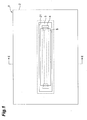
- Fig. 1 shows a plan view of a solid-state image pickup device according to the present embodiment.
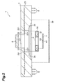
- Fig. 2 is a view showing, in an exploded manner, a section along a line II-II of the solid-state image pickup device according to the present embodiment shown in Fig. 1 .
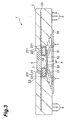
- Fig. 3 shows an end view along the line II-II of the solid-state image pickup device according to the present embodiment shown in Fig. 1 .
- the solid-state image pickup device 1 has a rectangular platelike multilayer wiring board 2 (package), and there formed in a central portion of the multilayer wiring board 2 is an opening portion 21 that is opened from the front surface (light-incident surface) of the board to the back surface (a surface on the side opposite to the light-incident surface) and extended in the longitudinal direction thereof. Moreover, there provided in the opening portion 21 of the multilayer wiring board 2 is a mounting portion 22 so as to protrude into the opening portion along the front surface of the board. To the mounting portion 22, a CCD chip 4 (solid-state image pickup element) is fixed via a spacer 3 so as to have a light-incident surface at the back surface side.
- a CCD chip 4 solid-state image pickup element
- a lens 5 (optical element) is fixed to the spacer 3 so as to oppose the back surface side of the CCD chip 4. Further, a cover member 20 to cover the opening portion is fixed at the back surface side of the multilayer wiring board 2.
- the multilayer wiring board 2 is formed by stacking upward in sequence a plurality of ceramic layers respectively having rectangular opening parts different in size so that the size of the opening parts becomes smaller as it goes upward. Then, the opening parts formed in the respective ceramic layers are overlapped to form the opening portion 21 extended stepwise from the front surface side toward the back surface side of the board, and the mounting portion 22 is provided at the front surface side of the board, and a step portion 24 is provided at a further back surface side than the mounting portion 22. Moreover, a predetermined shape of internal wiring is formed between the ceramic layers.
- the mounting portion 22 provided in the opening portion 21 has a mounting face 221 facing the back surface side of the board, and on the mounting face 221, an electrode pad 231 (reference potential electrode) is formed.
- the electrode pad 231 is electrically connected with a ground wiring 23 that is formed inside the multilayer wiring board 2 and to be a ground potential (0V) as a reference potential.
- the reference potential is provided as the ground potential, the reference potential is not limited thereto, and may be provided as a potential applied with a predetermined voltage so as to be, for example, plus or minus 5V, 8V, or the like.
- the step portion 24 is formed of three steps, and on a plane portion of each step, formed is a bonding pad (not shown) for externally taking out the electrode (clock electrode, output electrode, shield electrode) of the CCD chip 4.
- the bonding pad is externally led out via internal wiring (not shown) of the multilayer wiring board 2, and the part from which the internal wiring is externally led out is fixedly attached with an electrode pin 6 for an external connection by brazing etc.
- the electrode of the CCD chip 4 and the bonding pad are connected via a bonding wire 7.
- the spacer 3 has a rectangular outline of an outer periphery larger than an inner periphery of the opening portion 21 provided at the front surface side of the multilayer wiring board 2, and is a construction that a ceramic element body 31 having a rectangular opening part of an inner periphery smaller than the inner periphery of the opening portion 21 is covered with a conductive film 32. Moreover, of the spacer 3, an outer peripheral edge portion of one end face is fixed across the entire periphery along the mounting face 221 of the multilayer wiring board 2. In that case, the electrode pad 231 formed on the mounting face 221 and the conductive film 32 (a part formed on one end face) of the spacer 3 are fixed in a face contact state by use of a conductive adhesive. Also, an inner peripheral edge portion of one end face of the spacer 3 reaches a state protruded from the mounting portion into the opening portion across the entire periphery to thereby form a face on which the lens 5 to be described later is mounted.
- the ceramic element body of the spacer 3 a material with high thermal conductivity and small thermal expansion coefficient is preferably used.
- aluminum nitride is used as the material of the ceramic element body.
- the ceramic element body 31 is processed with high accuracy so as to have a predetermined thickness.
- a metal material of Au, Cu, Al, or the like having a high electrical conductivity is preferably used. Because Al easily forms an oxide film and declines in electrical conductivity, either of Au and Cu is particularly preferable. In the present embodiment, Au is used to form the conductive film.
- a method for forming the conductive film a thin-film forming method such as plating and sputtering that can cover the front surface of the ceramic element body 31 with a conductive film at a uniform thickness is used.
- the CCD chip 4 is a back-illuminated CCD chip, which has a photosensitive portion 41 (for example, 4098 pixels of 130 ⁇ m ⁇ 18 ⁇ m disposed one-dimensionally) that converts light made incident to an electric charge at the front surface side, and in a region (inner region) at the back surface side including a region corresponding to the photosensitive portion 41, a low-profile part 42 trimmed thin to a thickness of approximately 10 ⁇ m to 30 ⁇ m is formed. Also, the low-profile part 42 is a region to receive light, and the region is formed smaller than the opening part of the spacer 3.
- a photosensitive portion 41 for example, 4098 pixels of 130 ⁇ m ⁇ 18 ⁇ m disposed one-dimensionally
- the CCD chip 4 is fixed to the other end face of the spacer 3 fixed to the multilayer wiring board 2 (end face on the side opposite to the end face of the spacer 3 fixed to the mounting face 221) so that the CCD chip 4 has a light-incident surface at the back surface side.
- the conductive film of the spacer 3 and a region (outer region) at the back surface side other than the low-profile part 42 of the CCD chip 4 are fixed so as to make face contact with each other by use of a conductive adhesive.
- the back surface of the CCD chip 4 is electrically connected with the ground wiring of the multilayer wiring board 2 via the conductive film of the spacer 3 and the electrode pad (reference potential electrode) of the multilayer wiring board 2.
- the structure having the low-profile part 42 is formed by, first, depositing a silicon nitride film on a silicon substrate, patterning this into a desired shape through a photolithography process, and using the same as a mask for etching of the silicon substrate by an etchant made of KOH with a substrate periphery covered with the silicon nitride film being left thick.
- the lens 5 is for making light incident into the CCD chip 4, and there formed are microlenses with a pitch corresponding to that of the pixels formed on the photosensitive portion 41 of the CCD chip 4. Moreover, the lens 5 has a rectangular outline of an outer periphery smaller than the inner periphery of the opening portion 21 at the front surface side of the multilayer wiring board 2, and is fixed by use of an adhesive, inside the opening portion 21, to the inner peripheral edge portion (region of one end face protruded from the mounting portion into the opening portion) of one end face of the spacer 3 so as to be arranged opposed to the back surface of the CCD chip 4.
- one end of the spacer 3 is fixed with the CCD chip 4 and the other end is fixed with the lens 5, and thus the separation distance between the CCD chip 4 and the lens 5 is to be determined by the thickness of the spacer 3.
- the spacer 3 it is possible to improve the dimensional accuracy of the thickness since machining thereof is easy. Accordingly, the accuracy of the separation distance between the CCD chip 4 and the lens 5 can be improved independent of the molding accuracy of the multilayer wiring board 2.
- the spacer 3 has a high electrical conductivity and a high thermal conductivity since this is covered with the conductive film 32.
- the conductive film 32 of the spacer 3 and the electrode pad 231 (reference potential electrode) exposed into the opening portion 21 of the multilayer wiring board 2 are joined in a face contact state and the conductive film 32 of the spacer 3 and the CCD chip 4 are joined in a face contact state, and thus there is also a high thermal conductivity and electrical conductivity at the contact parts. Accordingly, the reference potential (ground potential in the present embodiment) of the CCD chip 4 is stabilized, and heat radiation of the CCD chip 4 is improved so that electrical characteristics of the CCD chip 4 are stabilized.
- the spacer 3 is to have a high thermal conductivity and a small thermal expansion coefficient. Accordingly, heat radiation of the CCD chip 4 is improved so that electrical characteristics of the CCD chip 4 are stabilized, and a fluctuation in separation distance between the CCD chip 4 and the lens 5 becomes considerably small.
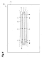
- Fig. 4 shows a plan view of a solid-state image pickup device according to the present embodiment.
- the first embodiment is further provided, in a region at the back surface side other than the low-profile part 42 of the CCD chip 4 and a non-imaging region of the light-incident surface of the lens 5, with positional alignment marks 71, 82 for positional alignment in their respective planar directions (planar directions orthogonal to the thickness direction of the multilayer wiring board).
- the positional alignment mark to be formed on the CCD chip 4 can be formed, when forming the low-profile part 42 on the back surface, by applying patterning through a photolithography process and etching also at the site to form the positional alignment mark.
- Positioning between the CCD chip 4 and the lens 5 can be performed by observing the position of the positional alignment mark 71 of the CCD chip 4 and the position of the positional alignment mark 82 of the lens 5 and adjusting the position of the CCD chip 4 and the lens 5 so that the respective marks are coincident.
- the CCD chip 4 and the lens 5 are provided with the positional alignment marks 71, 82, respectively, and thus an adjustment of the positional relationship between the CCD chip 4 and the lens 5 is simplified at the time of assembly of the device. Accordingly, the CCD chip 4 and the lens 5 can be arranged on the multilayer wiring board 2 at a high accuracy.
- the present invention is by no means limited to the aforementioned embodiments.
- the solid-state image pickup device of the present embodiment may further include a gas flow device composed of a gas supply passage and a gas discharge passage. Even when a gas resulting from decomposition of a resin material or the like such as an adhesive is released into a space made of a CCD chip, a glass, and a spacer, the gas is discharged to the outside of the multilayer wiring board through the gas flow device, and thus the gas released from the adhesive is suppressed from adhering to the light emission surface of the lens or the light-incident surface of the CCD chip and condensing, so that a decline in transmittance of incident light is suppressed. As a result, a decline in photodetecting sensitivity of the CCD chip can be suppressed.
- a gas flow device composed of a gas supply passage and a gas discharge passage.
- a plurality of cutaway portions may be formed in an opening end portion on the light-incident surface side of the opening portion formed in the multilayer wiring board. Since a tool for lens mounting (for positional adjustment) such as tweezers can be inserted therein, workability when placing the lens on the spacer or performing a positional adjustment is improved.
Landscapes
- Engineering & Computer Science (AREA)
- Multimedia (AREA)
- Signal Processing (AREA)
- Physics & Mathematics (AREA)
- General Physics & Mathematics (AREA)
- Solid State Image Pick-Up Elements (AREA)
- Transforming Light Signals Into Electric Signals (AREA)
- Facsimile Heads (AREA)
- Production Of Multi-Layered Print Wiring Board (AREA)
- Camera Bodies And Camera Details Or Accessories (AREA)
Abstract
Description
- The present invention relates to a solid-state image pickup device, and more particularly, to a solid-state image pickup device with a back-illuminated solid-state image pickup element.
- For this type of solid-state image pickup device, an opening portion is provided at the center of a ceramic or resin package, a solid-state image pickup element is arranged in the opening portion, and an optical element such as a lens is arranged at a predetermined distance from the solid-state image pickup element (see
Patent Documents 1 to 3, for example). - Patent Document 1: Japanese Published Unexamined Patent Application No.
2001-197375 - Patent Document 2: Japanese Published Unexamined Patent Application No.
2002-231913 - Patent Document 3: Japanese Published Unexamined Patent Application No.
2004-328386 - Meanwhile, for the solid-state image pickup device, it is necessary to strictly control a separation distance between the solid-state image pickup element and optical element. In a common solid-state image pickup device, the solid-state image pickup element and the optical element are mounted in a package, and the separation distance between the solid-state image pickup element and lens depends on the molding accuracy of the package. For example, in the invention described in the
above Patent Document 1, a mounting portion having a stepped plurality of plane portions is formed in the opening portion of the package, and the solid-state image pickup element and the lens are respectively mounted on the mounting portion, so that the accuracy of the separation distance between the solid-state image pickup element and lens depends on the molding accuracy of the mounting portion to be formed in the opening portion of the package. - Although there are packages made of resin and made of ceramic, since the packages made of resin are not so high in the accuracy of molding dies, there is also a limit to the molding accuracy etc., of the packages (mounting portions). Moreover, the packages made of resin have large thermal expansion coefficients, and thus, in operation of the solid-state image pickup device, expand or contract due to heat from the solid-state image pickup device to fluctuate the separation distance. On the other hand, the packages made of ceramic are likely to have variation in molding accuracy, as these contract in the course of sintering. In this case, it can also be considered to process the part on which the solid-state image pickup element and the optical element are mounted, processing is difficult because the part has a relatively complex shape.
- Therefore, the present invention aims to provide a solid-state image pickup device that allows improving the dimensional accuracy of the separation distance between the solid-state image pickup element and optical element without depending on the molding accuracy etc., of the package.
- A solid-state image pickup device according to the present invention includes: a multilayer wiring board having an opening portion; a spacer covered with a conductive film and fixed to the multilayer wiring board in a state of making the conductive film face contact with a reference potential electrode exposed into the opening portion of the multilayer wiring board; a solid-state image pickup element fixed to the spacer in a state of face contact with the conductive film of the spacer, the solid-state image pickup element arranged in the opening portion; and an optical element fixed at a position opposing the solid-state image pickup element via the spacer, the optical element transmitting light into the opening portion.
- According to the present invention, one end face of the spacer is fixed with the solid-state image pickup element and the other end face is fixed with the optical element, and thus the separation distance between the solid-state image pickup element and the optical element is to be determined by the thickness of the spacer. As for the spacer, it is possible to improve the dimensional accuracy of the thickness since machining thereof is easy. Accordingly, the accuracy of the separation distance between the solid-state image pickup element and the optical element can be improved independent of the molding accuracy of the package.
- Moreover, the spacer has a high electrical conductivity and a high thermal conductivity since this is covered with the conductive film. In addition, the conductive film of the spacer and the reference potential electrode exposed into the opening portion of the multilayer wiring board are joined in a face contact state and the conductive film of the spacer and the solid-state image pickup element are joined in a face contact state, and thus there is also a high thermal conductivity and electrical conductivity at the contact parts. Accordingly, the reference potential of the solid-state image pickup element is stabilized, and heat radiation of the solid-state image pickup element is improved so that electrical characteristics of the solid-state image pickup element are stabilized.
- Moreover, it is preferable that solid-state image pickup device comprises a positional alignment mark on a light-incident surface of the optical element and a surface, opposing the optical element, of the solid-state image pickup element.
- According to this preferred solid-state image pickup device, since the optical element and solid-state image pickup element are provided with the positional alignment mark, an adjustment of the positional relationship between the solid-state image pickup element and the optical element is simplified at the time of assembly of the device. Accordingly, the solid-state image pickup element and optical element can be arranged on the multilayer wiring board with high accuracy.
- Moreover, for the solid-state image pickup device, it is preferable that the spacer has an element body made of aluminum nitride.
- According to this preferred solid-state image pickup device, since the element body to form the spacer is made of aluminum nitride with high thermal conductivity and small thermal expansion coefficient, the spacer is to have a high thermal conductivity and a small thermal expansion coefficient. Accordingly, heat radiation of the solid-state image pickup element is improved so that electrical characteristics of the solid-state image pickup element are stabilized, and a fluctuation in separation distance between the solid-state image pickup element and the optical element becomes considerably small.
- The present invention can provide a solid-state image pickup device that allows improving the accuracy of the separation distance between the solid-state image pickup element and optical element without depending on the molding accuracy of the package.
-
- [
Fig. 1 ] A plan view of a solid-state image pickup device according to a first embodiment. - [
Fig. 2 ] A view showing, in an exploded manner, a section along a line II-II of the solid-state image pickup device according to the first embodiment shown inFig. 1 . - [
Fig. 3 ] An end view along the line II-II of the solid-state image pickup device according to the first embodiment shown inFig. 1 . - [
Fig. 4 ] A plan view of a solid-state image pickup device according to a second embodiment. - 1, 10··· solid-state image pickup device, 2··· multilayer wiring board, 3··· spacer, 4··· CCD chip (solid-state image pickup element), 5··· lens (optical element), 6···electrode pin for external connection, 7··· bonding wire, 71, 82··· positional alignment mark.
- The findings of the present invention can be easily understood in view of the following detailed descriptions with reference to the accompanying drawings, which are given by way of illustration only. Embodiments of the present invention will now be explained with reference to the accompanying drawings. When possible, parts identical to each other will be referred to with reference numerals identical to each other, and overlapping explanations will be omitted.
- (First Embodiment) Referring to
Fig. 1 to Fig. 3 , a solid-state image pickup device, which is a first embodiment, will be explained.Fig. 1 shows a plan view of a solid-state image pickup device according to the present embodiment.Fig. 2 is a view showing, in an exploded manner, a section along a line II-II of the solid-state image pickup device according to the present embodiment shown inFig. 1 .Fig. 3 shows an end view along the line II-II of the solid-state image pickup device according to the present embodiment shown inFig. 1 . - The solid-state
image pickup device 1 has a rectangular platelike multilayer wiring board 2 (package), and there formed in a central portion of themultilayer wiring board 2 is anopening portion 21 that is opened from the front surface (light-incident surface) of the board to the back surface (a surface on the side opposite to the light-incident surface) and extended in the longitudinal direction thereof. Moreover, there provided in theopening portion 21 of themultilayer wiring board 2 is amounting portion 22 so as to protrude into the opening portion along the front surface of the board. To themounting portion 22, a CCD chip 4 (solid-state image pickup element) is fixed via aspacer 3 so as to have a light-incident surface at the back surface side. Moreover, a lens 5 (optical element) is fixed to thespacer 3 so as to oppose the back surface side of theCCD chip 4. Further, acover member 20 to cover the opening portion is fixed at the back surface side of themultilayer wiring board 2. The respective components will be explained in the following. - The
multilayer wiring board 2 is formed by stacking upward in sequence a plurality of ceramic layers respectively having rectangular opening parts different in size so that the size of the opening parts becomes smaller as it goes upward. Then, the opening parts formed in the respective ceramic layers are overlapped to form theopening portion 21 extended stepwise from the front surface side toward the back surface side of the board, and themounting portion 22 is provided at the front surface side of the board, and astep portion 24 is provided at a further back surface side than themounting portion 22. Moreover, a predetermined shape of internal wiring is formed between the ceramic layers. - The
mounting portion 22 provided in theopening portion 21 has amounting face 221 facing the back surface side of the board, and on themounting face 221, an electrode pad 231 (reference potential electrode) is formed. Theelectrode pad 231 is electrically connected with aground wiring 23 that is formed inside themultilayer wiring board 2 and to be a ground potential (0V) as a reference potential. Although, in the present embodiment, the reference potential is provided as the ground potential, the reference potential is not limited thereto, and may be provided as a potential applied with a predetermined voltage so as to be, for example, plus or minus 5V, 8V, or the like. - Moreover, the
step portion 24 is formed of three steps, and on a plane portion of each step, formed is a bonding pad (not shown) for externally taking out the electrode (clock electrode, output electrode, shield electrode) of theCCD chip 4. The bonding pad is externally led out via internal wiring (not shown) of themultilayer wiring board 2, and the part from which the internal wiring is externally led out is fixedly attached with anelectrode pin 6 for an external connection by brazing etc. The electrode of theCCD chip 4 and the bonding pad are connected via abonding wire 7. - The
spacer 3 has a rectangular outline of an outer periphery larger than an inner periphery of the openingportion 21 provided at the front surface side of themultilayer wiring board 2, and is a construction that aceramic element body 31 having a rectangular opening part of an inner periphery smaller than the inner periphery of the openingportion 21 is covered with aconductive film 32. Moreover, of thespacer 3, an outer peripheral edge portion of one end face is fixed across the entire periphery along the mountingface 221 of themultilayer wiring board 2. In that case, theelectrode pad 231 formed on the mountingface 221 and the conductive film 32 (a part formed on one end face) of thespacer 3 are fixed in a face contact state by use of a conductive adhesive. Also, an inner peripheral edge portion of one end face of thespacer 3 reaches a state protruded from the mounting portion into the opening portion across the entire periphery to thereby form a face on which thelens 5 to be described later is mounted. - For the ceramic element body of the
spacer 3, a material with high thermal conductivity and small thermal expansion coefficient is preferably used. In the present embodiment, aluminum nitride is used as the material of the ceramic element body. Moreover, since the thickness of thespacer 3 results in a separation distance between theCCD chip 4 and thelens 5, theceramic element body 31 is processed with high accuracy so as to have a predetermined thickness. - For the conductive film that covers the front surface of the
ceramic element body 31, a metal material of Au, Cu, Al, or the like having a high electrical conductivity is preferably used. Because Al easily forms an oxide film and declines in electrical conductivity, either of Au and Cu is particularly preferable. In the present embodiment, Au is used to form the conductive film. As a method for forming the conductive film, a thin-film forming method such as plating and sputtering that can cover the front surface of theceramic element body 31 with a conductive film at a uniform thickness is used. - The
CCD chip 4 is a back-illuminated CCD chip, which has a photosensitive portion 41 (for example, 4098 pixels of 130µm×18µm disposed one-dimensionally) that converts light made incident to an electric charge at the front surface side, and in a region (inner region) at the back surface side including a region corresponding to thephotosensitive portion 41, a low-profile part 42 trimmed thin to a thickness of approximately 10µm to 30µm is formed. Also, the low-profile part 42 is a region to receive light, and the region is formed smaller than the opening part of thespacer 3. - The
CCD chip 4 is fixed to the other end face of thespacer 3 fixed to the multilayer wiring board 2 (end face on the side opposite to the end face of thespacer 3 fixed to the mounting face 221) so that theCCD chip 4 has a light-incident surface at the back surface side. In that case, the conductive film of thespacer 3 and a region (outer region) at the back surface side other than the low-profile part 42 of theCCD chip 4 are fixed so as to make face contact with each other by use of a conductive adhesive.. Thereby, the back surface of theCCD chip 4 is electrically connected with the ground wiring of themultilayer wiring board 2 via the conductive film of thespacer 3 and the electrode pad (reference potential electrode) of themultilayer wiring board 2. - Also, in the back-illuminated
CCD chip 4, the structure having the low-profile part 42 is formed by, first, depositing a silicon nitride film on a silicon substrate, patterning this into a desired shape through a photolithography process, and using the same as a mask for etching of the silicon substrate by an etchant made of KOH with a substrate periphery covered with the silicon nitride film being left thick. - The
lens 5 is for making light incident into theCCD chip 4, and there formed are microlenses with a pitch corresponding to that of the pixels formed on thephotosensitive portion 41 of theCCD chip 4. Moreover, thelens 5 has a rectangular outline of an outer periphery smaller than the inner periphery of the openingportion 21 at the front surface side of themultilayer wiring board 2, and is fixed by use of an adhesive, inside the openingportion 21, to the inner peripheral edge portion (region of one end face protruded from the mounting portion into the opening portion) of one end face of thespacer 3 so as to be arranged opposed to the back surface of theCCD chip 4. - As in the above, according to the present embodiment, one end of the
spacer 3 is fixed with theCCD chip 4 and the other end is fixed with thelens 5, and thus the separation distance between theCCD chip 4 and thelens 5 is to be determined by the thickness of thespacer 3. Moreover, as for thespacer 3, it is possible to improve the dimensional accuracy of the thickness since machining thereof is easy. Accordingly, the accuracy of the separation distance between theCCD chip 4 and thelens 5 can be improved independent of the molding accuracy of themultilayer wiring board 2. - Moreover, the
spacer 3 has a high electrical conductivity and a high thermal conductivity since this is covered with theconductive film 32. In addition, theconductive film 32 of thespacer 3 and the electrode pad 231 (reference potential electrode) exposed into the openingportion 21 of themultilayer wiring board 2 are joined in a face contact state and theconductive film 32 of thespacer 3 and theCCD chip 4 are joined in a face contact state, and thus there is also a high thermal conductivity and electrical conductivity at the contact parts. Accordingly, the reference potential (ground potential in the present embodiment) of theCCD chip 4 is stabilized, and heat radiation of theCCD chip 4 is improved so that electrical characteristics of theCCD chip 4 are stabilized. - Moreover, since the element body to form the
spacer 3 is made of aluminum nitride with high thermal conductivity and small thermal expansion coefficient, thespacer 3 is to have a high thermal conductivity and a small thermal expansion coefficient. Accordingly, heat radiation of theCCD chip 4 is improved so that electrical characteristics of theCCD chip 4 are stabilized, and a fluctuation in separation distance between theCCD chip 4 and thelens 5 becomes considerably small. - (Second Embodiment) Next, referring to
Fig. 4 , a second embodiment will be explained.Fig. 4 shows a plan view of a solid-state image pickup device according to the present embodiment. For a solid-stateimage pickup device 10 of the present embodiment, the first embodiment is further provided, in a region at the back surface side other than the low-profile part 42 of theCCD chip 4 and a non-imaging region of the light-incident surface of thelens 5, with positional alignment marks 71, 82 for positional alignment in their respective planar directions (planar directions orthogonal to the thickness direction of the multilayer wiring board). The positional alignment mark to be formed on theCCD chip 4 can be formed, when forming the low-profile part 42 on the back surface, by applying patterning through a photolithography process and etching also at the site to form the positional alignment mark. - Positioning between the
CCD chip 4 and thelens 5 can be performed by observing the position of thepositional alignment mark 71 of theCCD chip 4 and the position of thepositional alignment mark 82 of thelens 5 and adjusting the position of theCCD chip 4 and thelens 5 so that the respective marks are coincident. - As in the above, according to the present embodiment, the
CCD chip 4 and thelens 5 are provided with the positional alignment marks 71, 82, respectively, and thus an adjustment of the positional relationship between theCCD chip 4 and thelens 5 is simplified at the time of assembly of the device. Accordingly, theCCD chip 4 and thelens 5 can be arranged on themultilayer wiring board 2 at a high accuracy. - In addition, the present invention is by no means limited to the aforementioned embodiments. For example, it is preferable to arrange a bonding wire drawn out of the shield electrode of a CCD chip between a bonding wire drawn out of the clock electrode of the CCD chip and a bonding wire drawn out of the output electrode of the CCD chip. This is because crosstalk between a clock signal and an output signal can be suppressed. Moreover, for the same reason, it is preferable to further perform an arrangement from the internal wiring to the external connection terminal so that a shield is sandwiched between the clock wiring and output wiring in the same manner as wire bonding.
- Moreover, the solid-state image pickup device of the present embodiment may further include a gas flow device composed of a gas supply passage and a gas discharge passage. Even when a gas resulting from decomposition of a resin material or the like such as an adhesive is released into a space made of a CCD chip, a glass, and a spacer, the gas is discharged to the outside of the multilayer wiring board through the gas flow device, and thus the gas released from the adhesive is suppressed from adhering to the light emission surface of the lens or the light-incident surface of the CCD chip and condensing, so that a decline in transmittance of incident light is suppressed. As a result, a decline in photodetecting sensitivity of the CCD chip can be suppressed.
- Moreover, a plurality of cutaway portions may be formed in an opening end portion on the light-incident surface side of the opening portion formed in the multilayer wiring board. Since a tool for lens mounting (for positional adjustment) such as tweezers can be inserted therein, workability when placing the lens on the spacer or performing a positional adjustment is improved.
Claims (3)
- A solid-state image pickup device comprising:a multilayer wiring board having an opening portion;a spacer covered with a conductive film and fixed to the multilayer wiring board in a state of making the conductive film face contact with a reference potential electrode exposed into the opening portion of the multilayer wiring board;a solid-state image pickup element fixed to the spacer in a state of face contact with the conductive film of the spacer, the solid-state image pickup element arranged in the opening portion; andan optical element fixed at a position opposing the solid-state image pickup element via the spacer, the optical element transmitting light into the opening portion.
- The solid-state image pickup device according to Claim 1, comprising a positional alignment mark on a light-incident surface of the optical element and a surface, opposing the optical element, of the solid-state image pickup element.
- The solid-state image pickup device according to either Claim 1 or Claim 2, wherein the spacer has an element body made of aluminum nitride.
Applications Claiming Priority (2)
| Application Number | Priority Date | Filing Date | Title |
|---|---|---|---|
| JP2006277900A JP4490406B2 (en) | 2006-10-11 | 2006-10-11 | Solid-state imaging device |
| PCT/JP2007/069677 WO2008044675A1 (en) | 2006-10-11 | 2007-10-09 | Solid-state imaging device |
Publications (3)
| Publication Number | Publication Date |
|---|---|
| EP2077581A1 true EP2077581A1 (en) | 2009-07-08 |
| EP2077581A4 EP2077581A4 (en) | 2011-05-25 |
| EP2077581B1 EP2077581B1 (en) | 2016-07-06 |
Family
ID=39282868
Family Applications (1)
| Application Number | Title | Priority Date | Filing Date |
|---|---|---|---|
| EP07829415.4A Active EP2077581B1 (en) | 2006-10-11 | 2007-10-09 | Solid-state imaging device |
Country Status (6)
| Country | Link |
|---|---|
| US (1) | US8094221B2 (en) |
| EP (1) | EP2077581B1 (en) |
| JP (1) | JP4490406B2 (en) |
| KR (1) | KR101386267B1 (en) |
| CN (1) | CN101517739B (en) |
| WO (1) | WO2008044675A1 (en) |
Families Citing this family (17)
| Publication number | Priority date | Publication date | Assignee | Title |
|---|---|---|---|---|
| US8975599B2 (en) * | 2007-05-03 | 2015-03-10 | Asml Netherlands B.V. | Image sensor, lithographic apparatus comprising an image sensor and use of an image sensor in a lithographic apparatus |
| JP2009064839A (en) * | 2007-09-04 | 2009-03-26 | Panasonic Corp | Optical device and manufacturing method thereof |
| TWI505703B (en) * | 2007-12-19 | 2015-10-21 | 新加坡恒立私人有限公司 | Optical module, wafer level package and manufacturing method thereof |
| JP5256790B2 (en) * | 2008-03-11 | 2013-08-07 | 富士通セミコンダクター株式会社 | Solid-state imaging device, manufacturing method of solid-state imaging device, and manufacturing method of camera module |
| JP5207938B2 (en) | 2008-05-15 | 2013-06-12 | 浜松ホトニクス株式会社 | Spectroscopic module and method for manufacturing spectral module |
| JP5205241B2 (en) | 2008-05-15 | 2013-06-05 | 浜松ホトニクス株式会社 | Spectroscopic module |
| JP5415060B2 (en) | 2008-05-15 | 2014-02-12 | 浜松ホトニクス株式会社 | Spectroscopic module |
| JP2009300418A (en) * | 2008-05-15 | 2009-12-24 | Hamamatsu Photonics Kk | Spectroscopic module |
| KR101123159B1 (en) * | 2010-07-06 | 2012-03-20 | 엘지이노텍 주식회사 | Camera module |
| EP2696575B1 (en) * | 2011-04-05 | 2018-10-10 | Panasonic Intellectual Property Management Co., Ltd. | Solid-state image pickup device, and method for manufacturing solid-state image pickup device |
| JP5794002B2 (en) * | 2011-07-07 | 2015-10-14 | ソニー株式会社 | Solid-state imaging device, electronic equipment |
| JP5907176B2 (en) | 2011-12-28 | 2016-04-26 | 株式会社ニコン | Imaging device |
| JP5692419B2 (en) * | 2012-01-27 | 2015-04-01 | 株式会社村田製作所 | Multilayer wiring board |
| JP5940887B2 (en) * | 2012-05-18 | 2016-06-29 | 浜松ホトニクス株式会社 | Solid-state imaging device |
| JP6035687B2 (en) | 2014-08-29 | 2016-11-30 | Smk株式会社 | The camera module |
| FR3086459B1 (en) | 2018-09-25 | 2021-10-29 | St Microelectronics Grenoble 2 | ELECTRONIC DEVICE INCLUDING AN OPTICAL CHIP AND MANUFACTURING PROCESS |
| FR3086460B1 (en) | 2018-09-25 | 2021-10-29 | St Microelectronics Grenoble 2 | ELECTRONIC DEVICE INCLUDING AN OPTICAL CHIP AND MANUFACTURING PROCESS |
Family Cites Families (15)
| Publication number | Priority date | Publication date | Assignee | Title |
|---|---|---|---|---|
| US6281572B1 (en) | 1997-12-05 | 2001-08-28 | The Charles Stark Draper Laboratory, Inc. | Integrated circuit header assembly |
| US6566745B1 (en) * | 1999-03-29 | 2003-05-20 | Imec Vzw | Image sensor ball grid array package and the fabrication thereof |
| JP2001197375A (en) * | 2000-01-12 | 2001-07-19 | Sony Corp | Solid-state imaging device and assembling method thereof |
| US6384473B1 (en) * | 2000-05-16 | 2002-05-07 | Sandia Corporation | Microelectronic device package with an integral window |
| TW454309B (en) * | 2000-07-17 | 2001-09-11 | Orient Semiconductor Elect Ltd | Package structure of CCD image-capturing chip |
| JP3738824B2 (en) * | 2000-12-26 | 2006-01-25 | セイコーエプソン株式会社 | OPTICAL DEVICE, ITS MANUFACTURING METHOD, AND ELECTRONIC DEVICE |
| JP4606610B2 (en) * | 2001-01-26 | 2011-01-05 | 浜松ホトニクス株式会社 | Back-illuminated semiconductor device and filler filling method |
| JP4619553B2 (en) * | 2001-01-30 | 2011-01-26 | 浜松ホトニクス株式会社 | Semiconductor device |
| JP4373695B2 (en) * | 2003-04-16 | 2009-11-25 | 浜松ホトニクス株式会社 | Manufacturing method of backside illuminated photodetector |
| JP4231328B2 (en) * | 2003-04-24 | 2009-02-25 | 浜松ホトニクス株式会社 | Solid-state imaging device |
| JP3768972B2 (en) * | 2003-04-28 | 2006-04-19 | 松下電器産業株式会社 | Solid-state imaging device and manufacturing method thereof |
| US7646075B2 (en) | 2004-08-31 | 2010-01-12 | Micron Technology, Inc. | Microelectronic imagers having front side contacts |
| US20080003926A1 (en) * | 2004-09-29 | 2008-01-03 | Fujifilm Corporation | Method of Grinding Multilayer Body and Method of Manufacturing Solid State Image Pickup Device |
| JP4304163B2 (en) * | 2005-03-09 | 2009-07-29 | パナソニック株式会社 | Imaging module and manufacturing method thereof |
| JP4451864B2 (en) * | 2006-07-11 | 2010-04-14 | 浜松ホトニクス株式会社 | Wiring board and solid-state imaging device |
-
2006
- 2006-10-11 JP JP2006277900A patent/JP4490406B2/en active Active
-
2007
- 2007-10-09 EP EP07829415.4A patent/EP2077581B1/en active Active
- 2007-10-09 US US12/445,011 patent/US8094221B2/en active Active
- 2007-10-09 KR KR1020097000935A patent/KR101386267B1/en active Active
- 2007-10-09 CN CN200780034244XA patent/CN101517739B/en active Active
- 2007-10-09 WO PCT/JP2007/069677 patent/WO2008044675A1/en not_active Ceased
Also Published As
| Publication number | Publication date |
|---|---|
| WO2008044675A1 (en) | 2008-04-17 |
| JP2008098367A (en) | 2008-04-24 |
| CN101517739B (en) | 2012-02-15 |
| EP2077581A4 (en) | 2011-05-25 |
| US8094221B2 (en) | 2012-01-10 |
| JP4490406B2 (en) | 2010-06-23 |
| EP2077581B1 (en) | 2016-07-06 |
| KR101386267B1 (en) | 2014-04-17 |
| KR20090076888A (en) | 2009-07-13 |
| CN101517739A (en) | 2009-08-26 |
| US20100053388A1 (en) | 2010-03-04 |
Similar Documents
| Publication | Publication Date | Title |
|---|---|---|
| US8094221B2 (en) | Solid-state imaging device | |
| US7556975B2 (en) | Method for manufacturing backside-illuminated optical sensor | |
| KR100824812B1 (en) | Compact camera module and manufacturing method thereof | |
| US7316937B2 (en) | Method for manufacturing a solid-state image sensing device, such as a CCD | |
| US8653612B2 (en) | Semiconductor device | |
| EP2136552A1 (en) | Solid-state imaging device and method for manufacturing the same | |
| JP2008263550A (en) | Solid-state imaging device and manufacturing method thereof | |
| US20100321544A1 (en) | Semiconductor device, camera module and method of manufacturing semiconductor device | |
| CN1722456B (en) | Image sensor package and manufacturing method thereof | |
| US20100231766A1 (en) | Imaging device | |
| US20050270405A1 (en) | Image pickup device and camera module | |
| JP2004229167A (en) | Manufacturing method of camera module | |
| EP2077583B1 (en) | Light detecting device | |
| US20120286385A1 (en) | Semiconductor device, camera module, and semiconductor device manufacturing method | |
| CN101490844B (en) | Wiring board and solid-state imaging device | |
| US8110802B2 (en) | Photodetecting device including base with positioning portion | |
| JP2003303944A (en) | Method for manufacturing solid-state imaging device | |
| CN120303602A (en) | Filter unit | |
| CN120303601A (en) | Filter unit | |
| CN120283190A (en) | Light filtering unit | |
| JP2003244559A (en) | Solid-state imaging device | |
| CN120418708A (en) | Light filtering unit |
Legal Events
| Date | Code | Title | Description |
|---|---|---|---|
| PUAI | Public reference made under article 153(3) epc to a published international application that has entered the european phase |
Free format text: ORIGINAL CODE: 0009012 |
|
| 17P | Request for examination filed |
Effective date: 20090422 |
|
| AK | Designated contracting states |
Kind code of ref document: A1 Designated state(s): AT BE BG CH CY CZ DE DK EE ES FI FR GB GR HU IE IS IT LI LT LU LV MC MT NL PL PT RO SE SI SK TR |
|
| A4 | Supplementary search report drawn up and despatched |
Effective date: 20110429 |
|
| 17Q | First examination report despatched |
Effective date: 20110617 |
|
| DAX | Request for extension of the european patent (deleted) | ||
| GRAP | Despatch of communication of intention to grant a patent |
Free format text: ORIGINAL CODE: EPIDOSNIGR1 |
|
| INTG | Intention to grant announced |
Effective date: 20160224 |
|
| GRAS | Grant fee paid |
Free format text: ORIGINAL CODE: EPIDOSNIGR3 |
|
| GRAA | (expected) grant |
Free format text: ORIGINAL CODE: 0009210 |
|
| AK | Designated contracting states |
Kind code of ref document: B1 Designated state(s): AT BE BG CH CY CZ DE DK EE ES FI FR GB GR HU IE IS IT LI LT LU LV MC MT NL PL PT RO SE SI SK TR |
|
| REG | Reference to a national code |
Ref country code: GB Ref legal event code: FG4D |
|
| REG | Reference to a national code |
Ref country code: AT Ref legal event code: REF Ref document number: 811250 Country of ref document: AT Kind code of ref document: T Effective date: 20160715 Ref country code: CH Ref legal event code: EP |
|
| REG | Reference to a national code |
Ref country code: IE Ref legal event code: FG4D |
|
| REG | Reference to a national code |
Ref country code: DE Ref legal event code: R096 Ref document number: 602007046916 Country of ref document: DE |
|
| REG | Reference to a national code |
Ref country code: FR Ref legal event code: PLFP Year of fee payment: 10 |
|
| REG | Reference to a national code |
Ref country code: NL Ref legal event code: MP Effective date: 20160706 |
|
| REG | Reference to a national code |
Ref country code: LT Ref legal event code: MG4D |
|
| REG | Reference to a national code |
Ref country code: AT Ref legal event code: MK05 Ref document number: 811250 Country of ref document: AT Kind code of ref document: T Effective date: 20160706 |
|
| PG25 | Lapsed in a contracting state [announced via postgrant information from national office to epo] |
Ref country code: LT Free format text: LAPSE BECAUSE OF FAILURE TO SUBMIT A TRANSLATION OF THE DESCRIPTION OR TO PAY THE FEE WITHIN THE PRESCRIBED TIME-LIMIT Effective date: 20160706 Ref country code: IS Free format text: LAPSE BECAUSE OF FAILURE TO SUBMIT A TRANSLATION OF THE DESCRIPTION OR TO PAY THE FEE WITHIN THE PRESCRIBED TIME-LIMIT Effective date: 20161106 Ref country code: IT Free format text: LAPSE BECAUSE OF FAILURE TO SUBMIT A TRANSLATION OF THE DESCRIPTION OR TO PAY THE FEE WITHIN THE PRESCRIBED TIME-LIMIT Effective date: 20160706 Ref country code: FI Free format text: LAPSE BECAUSE OF FAILURE TO SUBMIT A TRANSLATION OF THE DESCRIPTION OR TO PAY THE FEE WITHIN THE PRESCRIBED TIME-LIMIT Effective date: 20160706 Ref country code: NL Free format text: LAPSE BECAUSE OF FAILURE TO SUBMIT A TRANSLATION OF THE DESCRIPTION OR TO PAY THE FEE WITHIN THE PRESCRIBED TIME-LIMIT Effective date: 20160706 |
|
| PG25 | Lapsed in a contracting state [announced via postgrant information from national office to epo] |
Ref country code: PL Free format text: LAPSE BECAUSE OF FAILURE TO SUBMIT A TRANSLATION OF THE DESCRIPTION OR TO PAY THE FEE WITHIN THE PRESCRIBED TIME-LIMIT Effective date: 20160706 Ref country code: SE Free format text: LAPSE BECAUSE OF FAILURE TO SUBMIT A TRANSLATION OF THE DESCRIPTION OR TO PAY THE FEE WITHIN THE PRESCRIBED TIME-LIMIT Effective date: 20160706 Ref country code: BE Free format text: LAPSE BECAUSE OF NON-PAYMENT OF DUE FEES Effective date: 20160706 Ref country code: GR Free format text: LAPSE BECAUSE OF FAILURE TO SUBMIT A TRANSLATION OF THE DESCRIPTION OR TO PAY THE FEE WITHIN THE PRESCRIBED TIME-LIMIT Effective date: 20161007 Ref country code: PT Free format text: LAPSE BECAUSE OF FAILURE TO SUBMIT A TRANSLATION OF THE DESCRIPTION OR TO PAY THE FEE WITHIN THE PRESCRIBED TIME-LIMIT Effective date: 20161107 Ref country code: ES Free format text: LAPSE BECAUSE OF FAILURE TO SUBMIT A TRANSLATION OF THE DESCRIPTION OR TO PAY THE FEE WITHIN THE PRESCRIBED TIME-LIMIT Effective date: 20160706 Ref country code: AT Free format text: LAPSE BECAUSE OF FAILURE TO SUBMIT A TRANSLATION OF THE DESCRIPTION OR TO PAY THE FEE WITHIN THE PRESCRIBED TIME-LIMIT Effective date: 20160706 Ref country code: LV Free format text: LAPSE BECAUSE OF FAILURE TO SUBMIT A TRANSLATION OF THE DESCRIPTION OR TO PAY THE FEE WITHIN THE PRESCRIBED TIME-LIMIT Effective date: 20160706 |
|
| REG | Reference to a national code |
Ref country code: DE Ref legal event code: R097 Ref document number: 602007046916 Country of ref document: DE |
|
| PG25 | Lapsed in a contracting state [announced via postgrant information from national office to epo] |
Ref country code: EE Free format text: LAPSE BECAUSE OF FAILURE TO SUBMIT A TRANSLATION OF THE DESCRIPTION OR TO PAY THE FEE WITHIN THE PRESCRIBED TIME-LIMIT Effective date: 20160706 Ref country code: RO Free format text: LAPSE BECAUSE OF FAILURE TO SUBMIT A TRANSLATION OF THE DESCRIPTION OR TO PAY THE FEE WITHIN THE PRESCRIBED TIME-LIMIT Effective date: 20160706 |
|
| PLBE | No opposition filed within time limit |
Free format text: ORIGINAL CODE: 0009261 |
|
| STAA | Information on the status of an ep patent application or granted ep patent |
Free format text: STATUS: NO OPPOSITION FILED WITHIN TIME LIMIT |
|
| PG25 | Lapsed in a contracting state [announced via postgrant information from national office to epo] |
Ref country code: SK Free format text: LAPSE BECAUSE OF FAILURE TO SUBMIT A TRANSLATION OF THE DESCRIPTION OR TO PAY THE FEE WITHIN THE PRESCRIBED TIME-LIMIT Effective date: 20160706 Ref country code: DK Free format text: LAPSE BECAUSE OF FAILURE TO SUBMIT A TRANSLATION OF THE DESCRIPTION OR TO PAY THE FEE WITHIN THE PRESCRIBED TIME-LIMIT Effective date: 20160706 Ref country code: BG Free format text: LAPSE BECAUSE OF FAILURE TO SUBMIT A TRANSLATION OF THE DESCRIPTION OR TO PAY THE FEE WITHIN THE PRESCRIBED TIME-LIMIT Effective date: 20161006 Ref country code: CZ Free format text: LAPSE BECAUSE OF FAILURE TO SUBMIT A TRANSLATION OF THE DESCRIPTION OR TO PAY THE FEE WITHIN THE PRESCRIBED TIME-LIMIT Effective date: 20160706 |
|
| REG | Reference to a national code |
Ref country code: CH Ref legal event code: PL |
|
| 26N | No opposition filed |
Effective date: 20170407 |
|
| REG | Reference to a national code |
Ref country code: IE Ref legal event code: MM4A |
|
| PG25 | Lapsed in a contracting state [announced via postgrant information from national office to epo] |
Ref country code: CH Free format text: LAPSE BECAUSE OF NON-PAYMENT OF DUE FEES Effective date: 20161031 Ref country code: LI Free format text: LAPSE BECAUSE OF NON-PAYMENT OF DUE FEES Effective date: 20161031 |
|
| PG25 | Lapsed in a contracting state [announced via postgrant information from national office to epo] |
Ref country code: SI Free format text: LAPSE BECAUSE OF FAILURE TO SUBMIT A TRANSLATION OF THE DESCRIPTION OR TO PAY THE FEE WITHIN THE PRESCRIBED TIME-LIMIT Effective date: 20160706 Ref country code: LU Free format text: LAPSE BECAUSE OF NON-PAYMENT OF DUE FEES Effective date: 20161009 |
|
| REG | Reference to a national code |
Ref country code: FR Ref legal event code: PLFP Year of fee payment: 11 |
|
| PG25 | Lapsed in a contracting state [announced via postgrant information from national office to epo] |
Ref country code: IE Free format text: LAPSE BECAUSE OF NON-PAYMENT OF DUE FEES Effective date: 20161009 |
|
| PG25 | Lapsed in a contracting state [announced via postgrant information from national office to epo] |
Ref country code: CY Free format text: LAPSE BECAUSE OF FAILURE TO SUBMIT A TRANSLATION OF THE DESCRIPTION OR TO PAY THE FEE WITHIN THE PRESCRIBED TIME-LIMIT Effective date: 20160706 Ref country code: HU Free format text: LAPSE BECAUSE OF FAILURE TO SUBMIT A TRANSLATION OF THE DESCRIPTION OR TO PAY THE FEE WITHIN THE PRESCRIBED TIME-LIMIT; INVALID AB INITIO Effective date: 20071009 |
|
| PG25 | Lapsed in a contracting state [announced via postgrant information from national office to epo] |
Ref country code: MC Free format text: LAPSE BECAUSE OF FAILURE TO SUBMIT A TRANSLATION OF THE DESCRIPTION OR TO PAY THE FEE WITHIN THE PRESCRIBED TIME-LIMIT Effective date: 20160706 Ref country code: TR Free format text: LAPSE BECAUSE OF FAILURE TO SUBMIT A TRANSLATION OF THE DESCRIPTION OR TO PAY THE FEE WITHIN THE PRESCRIBED TIME-LIMIT Effective date: 20160706 Ref country code: MT Free format text: LAPSE BECAUSE OF NON-PAYMENT OF DUE FEES Effective date: 20161031 |
|
| REG | Reference to a national code |
Ref country code: FR Ref legal event code: PLFP Year of fee payment: 12 |
|
| P01 | Opt-out of the competence of the unified patent court (upc) registered |
Effective date: 20230509 |
|
| REG | Reference to a national code |
Ref country code: DE Ref legal event code: R079 Ref document number: 602007046916 Country of ref document: DE Free format text: PREVIOUS MAIN CLASS: H01L0027140000 Ipc: H10F0019500000 |
|
| PGFP | Annual fee paid to national office [announced via postgrant information from national office to epo] |
Ref country code: GB Payment date: 20250828 Year of fee payment: 19 |
|
| PGFP | Annual fee paid to national office [announced via postgrant information from national office to epo] |
Ref country code: FR Payment date: 20250908 Year of fee payment: 19 |
|
| PGFP | Annual fee paid to national office [announced via postgrant information from national office to epo] |
Ref country code: DE Payment date: 20250902 Year of fee payment: 19 |