EP2075849A2 - Transparent conductive film and solar cell using the same - Google Patents
Transparent conductive film and solar cell using the same Download PDFInfo
- Publication number
- EP2075849A2 EP2075849A2 EP08254052A EP08254052A EP2075849A2 EP 2075849 A2 EP2075849 A2 EP 2075849A2 EP 08254052 A EP08254052 A EP 08254052A EP 08254052 A EP08254052 A EP 08254052A EP 2075849 A2 EP2075849 A2 EP 2075849A2
- Authority
- EP
- European Patent Office
- Prior art keywords
- transparent conductive
- conductive film
- oxide
- oxygen
- solar cell
- Prior art date
- Legal status (The legal status is an assumption and is not a legal conclusion. Google has not performed a legal analysis and makes no representation as to the accuracy of the status listed.)
- Withdrawn
Links
Images
Classifications
-
- H—ELECTRICITY
- H10—SEMICONDUCTOR DEVICES; ELECTRIC SOLID-STATE DEVICES NOT OTHERWISE PROVIDED FOR
- H10F—INORGANIC SEMICONDUCTOR DEVICES SENSITIVE TO INFRARED RADIATION, LIGHT, ELECTROMAGNETIC RADIATION OF SHORTER WAVELENGTH OR CORPUSCULAR RADIATION
- H10F77/00—Constructional details of devices covered by this subclass
- H10F77/30—Coatings
- H10F77/306—Coatings for devices having potential barriers
- H10F77/311—Coatings for devices having potential barriers for photovoltaic cells
- H10F77/315—Coatings for devices having potential barriers for photovoltaic cells the coatings being antireflective or having enhancing optical properties
-
- C—CHEMISTRY; METALLURGY
- C04—CEMENTS; CONCRETE; ARTIFICIAL STONE; CERAMICS; REFRACTORIES
- C04B—LIME, MAGNESIA; SLAG; CEMENTS; COMPOSITIONS THEREOF, e.g. MORTARS, CONCRETE OR LIKE BUILDING MATERIALS; ARTIFICIAL STONE; CERAMICS; REFRACTORIES; TREATMENT OF NATURAL STONE
- C04B35/00—Shaped ceramic products characterised by their composition; Ceramics compositions; Processing powders of inorganic compounds preparatory to the manufacturing of ceramic products
- C04B35/01—Shaped ceramic products characterised by their composition; Ceramics compositions; Processing powders of inorganic compounds preparatory to the manufacturing of ceramic products based on oxide ceramics
- C04B35/453—Shaped ceramic products characterised by their composition; Ceramics compositions; Processing powders of inorganic compounds preparatory to the manufacturing of ceramic products based on oxide ceramics based on zinc, tin, or bismuth oxides or solid solutions thereof with other oxides, e.g. zincates, stannates or bismuthates
-
- C—CHEMISTRY; METALLURGY
- C23—COATING METALLIC MATERIAL; COATING MATERIAL WITH METALLIC MATERIAL; CHEMICAL SURFACE TREATMENT; DIFFUSION TREATMENT OF METALLIC MATERIAL; COATING BY VACUUM EVAPORATION, BY SPUTTERING, BY ION IMPLANTATION OR BY CHEMICAL VAPOUR DEPOSITION, IN GENERAL; INHIBITING CORROSION OF METALLIC MATERIAL OR INCRUSTATION IN GENERAL
- C23C—COATING METALLIC MATERIAL; COATING MATERIAL WITH METALLIC MATERIAL; SURFACE TREATMENT OF METALLIC MATERIAL BY DIFFUSION INTO THE SURFACE, BY CHEMICAL CONVERSION OR SUBSTITUTION; COATING BY VACUUM EVAPORATION, BY SPUTTERING, BY ION IMPLANTATION OR BY CHEMICAL VAPOUR DEPOSITION, IN GENERAL
- C23C14/00—Coating by vacuum evaporation, by sputtering or by ion implantation of the coating forming material
- C23C14/06—Coating by vacuum evaporation, by sputtering or by ion implantation of the coating forming material characterised by the coating material
- C23C14/08—Oxides
- C23C14/086—Oxides of zinc, germanium, cadmium, indium, tin, thallium or bismuth
-
- H—ELECTRICITY
- H10—SEMICONDUCTOR DEVICES; ELECTRIC SOLID-STATE DEVICES NOT OTHERWISE PROVIDED FOR
- H10F—INORGANIC SEMICONDUCTOR DEVICES SENSITIVE TO INFRARED RADIATION, LIGHT, ELECTROMAGNETIC RADIATION OF SHORTER WAVELENGTH OR CORPUSCULAR RADIATION
- H10F71/00—Manufacture or treatment of devices covered by this subclass
- H10F71/138—Manufacture of transparent electrodes, e.g. transparent conductive oxides [TCO] or indium tin oxide [ITO] electrodes
-
- H—ELECTRICITY
- H10—SEMICONDUCTOR DEVICES; ELECTRIC SOLID-STATE DEVICES NOT OTHERWISE PROVIDED FOR
- H10F—INORGANIC SEMICONDUCTOR DEVICES SENSITIVE TO INFRARED RADIATION, LIGHT, ELECTROMAGNETIC RADIATION OF SHORTER WAVELENGTH OR CORPUSCULAR RADIATION
- H10F77/00—Constructional details of devices covered by this subclass
- H10F77/20—Electrodes
- H10F77/244—Electrodes made of transparent conductive layers, e.g. transparent conductive oxide [TCO] layers
- H10F77/251—Electrodes made of transparent conductive layers, e.g. transparent conductive oxide [TCO] layers comprising zinc oxide [ZnO]
-
- C—CHEMISTRY; METALLURGY
- C04—CEMENTS; CONCRETE; ARTIFICIAL STONE; CERAMICS; REFRACTORIES
- C04B—LIME, MAGNESIA; SLAG; CEMENTS; COMPOSITIONS THEREOF, e.g. MORTARS, CONCRETE OR LIKE BUILDING MATERIALS; ARTIFICIAL STONE; CERAMICS; REFRACTORIES; TREATMENT OF NATURAL STONE
- C04B2235/00—Aspects relating to ceramic starting mixtures or sintered ceramic products
- C04B2235/02—Composition of constituents of the starting material or of secondary phases of the final product
- C04B2235/30—Constituents and secondary phases not being of a fibrous nature
- C04B2235/32—Metal oxides, mixed metal oxides, or oxide-forming salts thereof, e.g. carbonates, nitrates, (oxy)hydroxides, chlorides
- C04B2235/3284—Zinc oxides, zincates, cadmium oxides, cadmiates, mercury oxides, mercurates or oxide forming salts thereof
-
- C—CHEMISTRY; METALLURGY
- C04—CEMENTS; CONCRETE; ARTIFICIAL STONE; CERAMICS; REFRACTORIES
- C04B—LIME, MAGNESIA; SLAG; CEMENTS; COMPOSITIONS THEREOF, e.g. MORTARS, CONCRETE OR LIKE BUILDING MATERIALS; ARTIFICIAL STONE; CERAMICS; REFRACTORIES; TREATMENT OF NATURAL STONE
- C04B2235/00—Aspects relating to ceramic starting mixtures or sintered ceramic products
- C04B2235/02—Composition of constituents of the starting material or of secondary phases of the final product
- C04B2235/30—Constituents and secondary phases not being of a fibrous nature
- C04B2235/34—Non-metal oxides, non-metal mixed oxides, or salts thereof that form the non-metal oxides upon heating, e.g. carbonates, nitrates, (oxy)hydroxides, chlorides
- C04B2235/3409—Boron oxide, borates, boric acids, or oxide forming salts thereof, e.g. borax
-
- C—CHEMISTRY; METALLURGY
- C04—CEMENTS; CONCRETE; ARTIFICIAL STONE; CERAMICS; REFRACTORIES
- C04B—LIME, MAGNESIA; SLAG; CEMENTS; COMPOSITIONS THEREOF, e.g. MORTARS, CONCRETE OR LIKE BUILDING MATERIALS; ARTIFICIAL STONE; CERAMICS; REFRACTORIES; TREATMENT OF NATURAL STONE
- C04B2235/00—Aspects relating to ceramic starting mixtures or sintered ceramic products
- C04B2235/02—Composition of constituents of the starting material or of secondary phases of the final product
- C04B2235/30—Constituents and secondary phases not being of a fibrous nature
- C04B2235/40—Metallic constituents or additives not added as binding phase
-
- Y—GENERAL TAGGING OF NEW TECHNOLOGICAL DEVELOPMENTS; GENERAL TAGGING OF CROSS-SECTIONAL TECHNOLOGIES SPANNING OVER SEVERAL SECTIONS OF THE IPC; TECHNICAL SUBJECTS COVERED BY FORMER USPC CROSS-REFERENCE ART COLLECTIONS [XRACs] AND DIGESTS
- Y02—TECHNOLOGIES OR APPLICATIONS FOR MITIGATION OR ADAPTATION AGAINST CLIMATE CHANGE
- Y02E—REDUCTION OF GREENHOUSE GAS [GHG] EMISSIONS, RELATED TO ENERGY GENERATION, TRANSMISSION OR DISTRIBUTION
- Y02E10/00—Energy generation through renewable energy sources
- Y02E10/50—Photovoltaic [PV] energy
Definitions
- the present invention relates to a transparent conductive film having an improved crystallinity and to a solar cell using the transparent conductive film.
- a transparent conductive film formed of indium tin oxide (ITO) , zinc oxide (ZnO) or the like has been used in: display devices, such as an LCD device and an EL display device; photovoltaic devices, such as a solar cell and a photo sensor; semiconductor devices, such as a thin film transistor (TFT); and optical communication devices, such as an optical modulator and an optical switch.
- display devices such as an LCD device and an EL display device
- photovoltaic devices such as a solar cell and a photo sensor
- semiconductor devices such as a thin film transistor (TFT)
- optical communication devices such as an optical modulator and an optical switch.
- the transparent conductive film is used as an electrode for extracting photogenerated carriers from a photoelectric conversion layer that generates photogenerated carriers upon receiving light.
- the transparent conductive film is formed either on a light-receiving surface of the photoelectric conversion layer or on a back surface provided on the opposite side of the light-receiving surface.
- a transparent conductive film is placed between the two photoelectric conversion layers, and serves as a reflective layer that reflects back part of light transmitted through one of the two photoelectric conversion layers, toward the photoelectric conversion layer.
- Such a transparent conductive film needs to have both a high optical transparency and a high electric conductivity.
- Japanese Unexamined Patent Application Publication No. Hei 5-110125 proposes a technique in which the amount of dopant (for example, Al, In, B, or Ga) to enhance electric conductivity of a transparent conductive film is increased in a region of the transparent conductive film close to an interface with a photoelectric conversion layer. With such a technique, it becomes possible to reduce a contact resistance at the interface between the transparent conductive film and the photoelectric conversion layer.
- dopant for example, Al, In, B, or Ga
- an object of the present invention is to provide a transparent conductive film having an improved crystallinity and a solar cell using the transparent conductive film.
- An aspect of the present invention provides a transparent conductive film including: an oxide of a first element; a second element doped into the oxide of the first element; and a third element doped into the oxide of the first element.
- the oxide of the first element has optical transparency
- the bond distance between the second element and oxygen is shorter than the bond distance between the first element and oxygen
- the bond distance between the third element and oxygen is longer than the bond distance between the first element and oxygen.
- the oxide of the first element is preferably zinc oxide.
- the second element is preferably boron
- the third element is preferably gallium
- a solar cell including: a first photoelectric conversion layer configured to generate photogenerated carriers upon receiving light; and a transparent conductive film formed on the first photoelectric conversion layer.
- the transparent conductive film include: an oxide of a first element; a second element doped into the oxide of the first element; and a third element doped into the oxide of the first element.
- the oxide of the first element has optical transmission properties, the bond distance between the second element and oxygen is shorter than the bond distance between the first element and oxygen, and the bond distance between the third element and oxygen is longer than the bond distance between the first element and oxygen.
- the solar cell preferably further includes a second photoelectric conversion layer generating photogenerated carriers upon receiving light.
- the transparent conductive film may be placed between the first photoelectric conversion layer and the second photoelectric conversion layer.
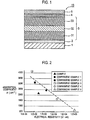
- Fig. 1 is a cross-sectional view of the solar cell 10 according to the embodiment of the present invention.
- the solar cell 10 includes a substrate 1, a light-receiving-surface electrode layer 2, a photoelectric conversion layer 3, a transparent conductive film 4, and a back-surface electrode layer 5.
- the light-receiving-surface electrode layer 2, the photoelectric conversion layer 3, the transparent conductive film 4, and the back-surface electrode layer 5 are sequentially stacked on the substrate 1.
- the substrate 1 is formed of a light-transmitting material having light transmission properties and electrical insulating properties, such as a glass or a plastic.
- the substrate 1 has a light-receiving surface and a back surface provided on the opposite side of the light-receiving surface.
- the light-receiving-surface electrode layer 2 is stacked on the back surface of the substrate 1.
- the light-receiving-surface electrode layer 2 serves as a first electrode of the photoelectric conversion layer 3.
- the light-receiving-surface electrode layer 2 is a transparent conductive film having light transmission properties and electric conductivity.
- a metal oxide such as tin oxide (SnO 2 ), zinc oxide (ZnO), indium oxide (In 2 O 3 ) or titanium oxide (TiO 2 ), can be used.
- a metal oxide, of these, doped with fluorine (F), tin (Sn), aluminum (Al), iron (Fe), gallium (Ga), niobium (Nb) or the like may be used.
- the photoelectric conversion layer 3 is formed by sequentially stacking a first semiconductor layer 31, a reflective layer 32 and a second semiconductor layer 33 on the light-receiving-surface electrode layer 2.
- the first semiconductor layer 31 generates photogenerated carriers upon receiving light entering from the light-receiving-surface electrode layer 2.
- the first semiconductor layer 31 is formed by sequentially stacking a p-type silicon semiconductor, an i-type amorphous silicon semiconductor and an n-type silicon semiconductor (not shown) on the light-receiving-surface electrode layer 2. Accordingly, the first semiconductor layer 31 has a pin junction.
- the reflective layer 32 reflects back part of light transmitted through the first semiconductor layer 31, toward the first semiconductor layer 31.
- the reflective layer 32 serves as an electrode electrically connecting the first semiconductor layer 31 and the second semiconductor layer 33.
- the reflective layer 32 is a transparent conductive film having light transmission properties and electric conductivity, and can be formed of the same material as that of the light-receiving-surface electrode layer 2.
- the second semiconductor layer 33 generates photogenerated carriers upon receiving light entering from the reflective layer 32.
- the second semiconductor layer 33 is formed by sequentially stacking a p-type silicon semiconductor, an i-type microcrystalline silicon semiconductor and an n-type silicon semiconductor (not shown) on the reflective layer 32. Accordingly, the second semiconductor layer 33 has a pin junction.
- an amorphous silicon semiconductor and a microcrystalline silicon semiconductor absorb lights having different wavelengths from each other. Accordingly, a tandem solar cell having two kinds of stacked semiconductor layers can effectively utilize sunlight spectrum.
- the second semiconductor layer 33 is not limited to the above-described microcrystalline silicon semiconductor; alternatively, a single crystal silicon semiconductor or a polycrystalline silicon semiconductor can be used, instead.
- the transparent conductive film 4 is stacked on the photoelectric conversion layer 3.
- the transparent conductive film 4 serves as a second electrode of the photoelectric conversion layer 3.
- the transparent conductive film 4 can be formed of a base material doped with two or more dopants.
- a base material is a metal oxide having light transmission properties and electric conductivity, such as tin oxide (SnO 2 ), zinc oxide (ZnO), or indium oxide (In 2 O 3 ).
- Such dopants improve electric conductivity and crystallinity of the transparent conductive film 4. A detailed configuration of the transparent conductive film 4 will be described later.
- the back-surface electrode layer 5 is stacked on the transparent conductive film 4, and serves as the second electrode of the photoelectric conversion layer 3. In addition, the back-surface electrode layer 5 reflects back light transmitted through the second semiconductor layer 33 and the transparent conductive film 4, toward the second semiconductor layer 33.
- a metal material having electric conductivity and high reflectivity such as aluminum (Al), silver (Ag), or cupper (Cu), can be used.
- the light-receiving-surface electrode layer 2, the photoelectric conversion layer 3, the transparent conductive film 4, and the back-surface electrode layer 5 can be sequentially stacked, while patterned by a well known laser patterning method.
- the laser patterning method allows formation of an integrated solar cell which is composed of multiple solar cell elements electrically connected in series.
- the transparent conductive film 4 includes an oxide of a first element a as a base material.
- the first element a is selected from Sn, Zn, In, and the like; thus, the base material may be tin oxide (SnO 2 ), zinc oxide (ZnO), indium oxide (In 2 O 3 ), or the like.
- the transparent conductive film 4 is doped with two kinds of dopants, that is, a second element B and a third element Y.
- the second element B and the third element ⁇ are doped into the oxide of the first element ⁇ , and bond to oxygen. Table 1 shows combinations of such an oxide of a first element ⁇ , a second element B, and a third element ⁇ .
- Table 1 shows the bond distance ⁇ -O of the first element a to oxygen O, the bond distance B-O of the second element B to oxygen O, and the bond distance ⁇ -O of the third element ⁇ to oxygen O in each of the oxides of the first elements ⁇ .
- the distance ⁇ -O is shorter than the distance ⁇ -O, whereas the distance ⁇ -O is longer than the distance ⁇ -O.
- the light-receiving-surface electrode layer 2 is formed on the substrate 1 by thermal CVD method or sputtering method.
- the light-receiving-surface electrode layer 2 is, for example, a SnO 2 film having a thickness of 500 to 800 nm.
- the first semiconductor layer 31 is formed by sequentially stacking p-, i-, and n-type amorphous silicon semiconductors on the light-receiving-surface electrode layer 2 by plasma CVD method.
- the reflective layer 32 is formed on the first semiconductor layer 31 by sputtering method or film coating method.
- the reflective layer 32 is, for example, a ZnO film having a thickness of 100 nm or less.
- the second semiconductor layer 33 is formed by sequentially stacking p-, i-, and n-type microcrystalline silicon semiconductors on the reflective layer 32 by plasma CVD method.
- the transparent conductive film 4 is formed on the second semiconductor layer 33 by RF sputtering method. Specifically, a reaction chamber of an RF sputtering apparatus is pre-evacuated until the inside pressure reaches 3x10 -6 Torr or even below. Next, the reaction chamber is supplied with Ar gas until the inside pressure reaches approximately 3x10 -3 Torr. Subsequently electricity is simultaneously discharged to both a B-doped ZnO target (BZO) and a Ga-doped ZnO target (GZO) by use of an RF power of 400 W. With this operation, B and Ga are doped into ZnO serving as a base material, and the B and Ga bond to oxygen O in ZnO. Such a transparent conductive film 4 is formed in a thickness of 100 nm or less.
- the distance Zn-O of Zn to O is 1.95 ⁇
- the distance B-O of B to O is 1.363 ⁇
- the distance Ga-O of Ga to O is 2.08 ⁇ .
- the distance ß-O is shorter than the distance ⁇ -O
- the distance ⁇ -O is longer than the distance ⁇ -O.
- the back-surface electrode layer 5 is formed on the transparent conductive film 4 by sputtering method or film coating method.
- the back-surface electrode layer 5 is, for example, an Ag film having a thickness of 100 to 300 nm.
- the light-receiving-surface electrode layer 2, the photoelectric conversion layer 3, the transparent conductive film 4, and the back-surface electrode layer 5 may be patterned by a well-known laser patterning method.
- the transparent conductive film 4 provided to the solar cell 10 according to the present invention includes an oxide of the first element ⁇ , the second element ⁇ , and the third element ⁇ . Both the second element ⁇ and the third element ⁇ are doped into the oxide of the first element ⁇ .
- the bond distance ß-O of the second element ⁇ to oxygen O is shorter than the bond distance ⁇ -O of the first element ⁇ to oxygen O
- the bond distance ⁇ -O of the third element ⁇ to oxygen O is longer than the bond distance ⁇ -O of the first element ⁇ to oxygen O.
- lattice strain occurs in the transparent conductive film.
- a bond distance X-O of the element of the base material to oxygen in the transparent conductive film is different from a bond distance Y-O of the element of the dopant to oxygen.
- shrinkage strain occurs when the bond distance Y-O is shorter than the bond distance X-O.
- expansion strain occurs when the bond distance Y-O is longer than the bond distance X-O.
- the second and third elements are doped into the oxide of the first element ⁇ serving as the base material in this embodiment.
- the resulting the bond distance ß-O of the second element to oxygen is shorter the distance ⁇ -O
- the resulting bond distance ⁇ -O of the third element to oxygen is longer than the distance ⁇ -O.
- the shrinkage strain and the expansion strain in the transparent conductive film can be cancelled against each other, while reducing a contact resistance at the interface between the transparent conductive film 4 and the photoelectric conversion layer 3. As a result, it becomes possible to improve the crystallinity of the transparent conductive film 4.
- the second and third elements are doped into the oxide of the first element in the above-described embodiment.
- three or more kinds of dopants can be used as appropriate.
- the transparent conductive film 4 used in the solar cell 10 is described as an example.
- the above-described transparent conductive film 4 can be applied to: display devices, such as an LCD device and an EL display device; photovoltaic devices, such as a photo sensor; semiconductor devices, such as TFT; optical communication devices, such as an optical modulator and an optical switch.
- the transparent conductive film 4 used in the thin film solar cell 10 is described as an example.
- the transparent conductive film 4 can be applied to general solar cells, such as a crystalline solar cell and a compound semiconductor solar cell.
- the transparent conductive film 4 is described as an example.
- the transparent conductive film 4 may be used as the reflective layer 32 placed between the first semiconductor layer 31 and the second semiconductor layer 33. Accordingly, it becomes possible to improve the crystallinity of the reflective layer 32, while reducing a contact resistance both at the interface between the reflective layer 32 and the first semiconductor layer31, and at the interface between the reflective layer 32 and the second semiconductor layer 33.
- the transparent conductive film 4 may be used as the light-receiving-surface electrode layer 2 placed between the substrate 1 and the first semiconductor layer 31. Accordingly, it becomes possible to improve the crystallinity of the light-receiving-surface electrode layer 2, while reducing the contact resistance at the interface between the light-receiving-surface electrode layer 2 and the photoelectric conversion layer 3.
- the tandem solar cell 10 is described as an example.
- the solar cell 10 may be a solar cell with a single semiconductor layer or with three or more semiconductor layers.
- Example a solar cell according to the present invention will be concretely described by way of Example. Note that the present invention is not limited to that to be shown in Example below, and can be implemented with appropriate modifications within a range not departing from the scope of the present invention.
- a transparent conductive film according to Example of the present invention was manufactured as follows:
- a reaction chamber of an RF sputtering apparatus was pre-evacuated until the inside pressure reaches 3x10 -6 Torr.
- the reaction chamber was supplied with Ar gas until the inside pressure reaches approximately 3x10 -3 Torr.
- electricity was simultaneously discharged to both a ZnO target doped 4wt% B 2 O 3 (BZO) and a ZnO target doped 4wt% Ga 2 O 3 (GZO) by use of an RF power of 400 W.
- B and Ga were doped into ZnO serving as a base material.
- a transparent conductive film (GZO + BZO) having a thickness of 100 nm was formed on a glass substrate.
- Three kinds of transparent conductive films (GZO) with different amounts of Ga were formed by use of a Ga-doped ZnO target (GZO) in an RF sputtering apparatus under the same condition as in Example. Specifically, 2 wt%, 4 wt% and 6 wt% of Ga were respectively doped into the transparent conductive films of Comparative Examples 1 to 3. The thickness of each of the transparent conductive films was 100 nm.
- a transparent conductive film of Comparative Example 4 was formed by use of a ZnO target doped B 2 O 3 (BZO) in an RF sputtering apparatus under the same condition as in Example.
- BZO ZnO target doped B 2 O 3
- 4 wt% of B was doped into the transparent conductive film, and the thickness of the film was 100 nm.
- a transparent conductive film of Comparative Example 5 was formed by use of a non-doped ZnO target in an RF sputtering apparatus under the same condition as in Example.
- the transparent conductive film according to Example can achieve both a high electric conductivity and a high optical transmission property, both of which are important properties for a transparent conductive film.
Landscapes
- Chemical & Material Sciences (AREA)
- Engineering & Computer Science (AREA)
- Materials Engineering (AREA)
- Organic Chemistry (AREA)
- Ceramic Engineering (AREA)
- Chemical Kinetics & Catalysis (AREA)
- Mechanical Engineering (AREA)
- Metallurgy (AREA)
- Manufacturing & Machinery (AREA)
- Structural Engineering (AREA)
- Photovoltaic Devices (AREA)
- Non-Insulated Conductors (AREA)
Abstract
Description
- The present invention relates to a transparent conductive film having an improved crystallinity and to a solar cell using the transparent conductive film.
- Conventionally, a transparent conductive film formed of indium tin oxide (ITO) , zinc oxide (ZnO) or the like has been used in: display devices, such as an LCD device and an EL display device; photovoltaic devices, such as a solar cell and a photo sensor; semiconductor devices, such as a thin film transistor (TFT); and optical communication devices, such as an optical modulator and an optical switch.
- In a solar cell, for example, the transparent conductive film is used as an electrode for extracting photogenerated carriers from a photoelectric conversion layer that generates photogenerated carriers upon receiving light. Specifically, the transparent conductive film is formed either on a light-receiving surface of the photoelectric conversion layer or on a back surface provided on the opposite side of the light-receiving surface.
- In a tandem solar cell having two photoelectric conversion layers, a transparent conductive film is placed between the two photoelectric conversion layers, and serves as a reflective layer that reflects back part of light transmitted through one of the two photoelectric conversion layers, toward the photoelectric conversion layer.
- Accordingly, such a transparent conductive film needs to have both a high optical transparency and a high electric conductivity.
- To fulfill the needs, Japanese Unexamined Patent Application Publication No.
Hei 5-110125 - However, in such a region where an increased amount of dopant is doped, significant lattice defect is caused due to the addition of the dopant. This results in lattice strain in the transparent conductive film, causing a decrease in crystallinity of the transparent conductive film.
- The present invention has been made in view of the above-described problem. Accordingly, an object of the present invention is to provide a transparent conductive film having an improved crystallinity and a solar cell using the transparent conductive film.
- An aspect of the present invention provides a transparent conductive film including: an oxide of a first element; a second element doped into the oxide of the first element; and a third element doped into the oxide of the first element. In the transparent conductive film, the oxide of the first element has optical transparency, the bond distance between the second element and oxygen is shorter than the bond distance between the first element and oxygen, and the bond distance between the third element and oxygen is longer than the bond distance between the first element and oxygen.
- According to another aspect of the present invention, the oxide of the first element is preferably zinc oxide.
- According to another aspect of the present invention, the second element is preferably boron, and the third element is preferably gallium.
- Moreover, another aspect of the present invention provides a solar cell including: a first photoelectric conversion layer configured to generate photogenerated carriers upon receiving light; and a transparent conductive film formed on the first photoelectric conversion layer. In the solar cell, the transparent conductive film include: an oxide of a first element; a second element doped into the oxide of the first element; and a third element doped into the oxide of the first element. In the transparent conductive film, the oxide of the first element has optical transmission properties, the bond distance between the second element and oxygen is shorter than the bond distance between the first element and oxygen, and the bond distance between the third element and oxygen is longer than the bond distance between the first element and oxygen.
- According to another aspect of the present invention, the solar cell preferably further includes a second photoelectric conversion layer generating photogenerated carriers upon receiving light. In the solar cell, the transparent conductive film may be placed between the first photoelectric conversion layer and the second photoelectric conversion layer.
-
-
Fig. 1 is a cross-sectional view of asolar cell 10 according to an embodiment of the present invention. -
Fig. 2 is a graph showing relationships between electrical resistivity and absorption coefficient according to Examples of the present invention. - Embodiments of the present invention will be described with reference to the drawings. In the following description of the drawings, identical or similar constituents are designated by identical or similar reference numerals. Note that the drawings are merely schematic and proportions of the dimensions and the like are different from the actual ones. Accordingly, the concrete dimensions and the like should be determined in consideration of the following description of the invention. Moreover, it is needless to say that dimensional relations or proportions may vary among the drawings.
- Hereinafter, a configuration of a
solar cell 10 according to an embodiment of the present invention will be described with reference toFig. 1 . -
Fig. 1 is a cross-sectional view of thesolar cell 10 according to the embodiment of the present invention. As shown inFig. 1 , thesolar cell 10 includes asubstrate 1, a light-receiving-surface electrode layer 2, aphotoelectric conversion layer 3, a transparent conductive film 4, and a back-surface electrode layer 5. The light-receiving-surface electrode layer 2, thephotoelectric conversion layer 3, the transparent conductive film 4, and the back-surface electrode layer 5 are sequentially stacked on thesubstrate 1. - The
substrate 1 is formed of a light-transmitting material having light transmission properties and electrical insulating properties, such as a glass or a plastic. Thesubstrate 1 has a light-receiving surface and a back surface provided on the opposite side of the light-receiving surface. - The light-receiving-
surface electrode layer 2 is stacked on the back surface of thesubstrate 1. The light-receiving-surface electrode layer 2 serves as a first electrode of thephotoelectric conversion layer 3. The light-receiving-surface electrode layer 2 is a transparent conductive film having light transmission properties and electric conductivity. For the light-receiving-surface electrode layer 2, a metal oxide such as tin oxide (SnO2), zinc oxide (ZnO), indium oxide (In2O3) or titanium oxide (TiO2), can be used. In addition, a metal oxide, of these, doped with fluorine (F), tin (Sn), aluminum (Al), iron (Fe), gallium (Ga), niobium (Nb) or the like may be used. - The
photoelectric conversion layer 3 is formed by sequentially stacking afirst semiconductor layer 31, areflective layer 32 and asecond semiconductor layer 33 on the light-receiving-surface electrode layer 2. - The
first semiconductor layer 31 generates photogenerated carriers upon receiving light entering from the light-receiving-surface electrode layer 2. Thefirst semiconductor layer 31 is formed by sequentially stacking a p-type silicon semiconductor, an i-type amorphous silicon semiconductor and an n-type silicon semiconductor (not shown) on the light-receiving-surface electrode layer 2. Accordingly, thefirst semiconductor layer 31 has a pin junction. - The
reflective layer 32 reflects back part of light transmitted through thefirst semiconductor layer 31, toward thefirst semiconductor layer 31. In addition, thereflective layer 32 serves as an electrode electrically connecting thefirst semiconductor layer 31 and thesecond semiconductor layer 33. Thereflective layer 32 is a transparent conductive film having light transmission properties and electric conductivity, and can be formed of the same material as that of the light-receiving-surface electrode layer 2. - The
second semiconductor layer 33 generates photogenerated carriers upon receiving light entering from thereflective layer 32. Thesecond semiconductor layer 33 is formed by sequentially stacking a p-type silicon semiconductor, an i-type microcrystalline silicon semiconductor and an n-type silicon semiconductor (not shown) on thereflective layer 32. Accordingly, thesecond semiconductor layer 33 has a pin junction. - Here, an amorphous silicon semiconductor and a microcrystalline silicon semiconductor absorb lights having different wavelengths from each other. Accordingly, a tandem solar cell having two kinds of stacked semiconductor layers can effectively utilize sunlight spectrum. Note that the
second semiconductor layer 33 is not limited to the above-described microcrystalline silicon semiconductor; alternatively, a single crystal silicon semiconductor or a polycrystalline silicon semiconductor can be used, instead. - The transparent conductive film 4 is stacked on the
photoelectric conversion layer 3. The transparent conductive film 4 serves as a second electrode of thephotoelectric conversion layer 3. The transparent conductive film 4 can be formed of a base material doped with two or more dopants. Such a base material is a metal oxide having light transmission properties and electric conductivity, such as tin oxide (SnO2), zinc oxide (ZnO), or indium oxide (In2O3). Such dopants improve electric conductivity and crystallinity of the transparent conductive film 4. A detailed configuration of the transparent conductive film 4 will be described later. - The back-
surface electrode layer 5 is stacked on the transparent conductive film 4, and serves as the second electrode of thephotoelectric conversion layer 3. In addition, the back-surface electrode layer 5 reflects back light transmitted through thesecond semiconductor layer 33 and the transparent conductive film 4, toward thesecond semiconductor layer 33. For the back-surface electrode layer 5, a metal material having electric conductivity and high reflectivity, such as aluminum (Al), silver (Ag), or cupper (Cu), can be used. - Here, the light-receiving-
surface electrode layer 2, thephotoelectric conversion layer 3, the transparent conductive film 4, and the back-surface electrode layer 5 can be sequentially stacked, while patterned by a well known laser patterning method. The laser patterning method allows formation of an integrated solar cell which is composed of multiple solar cell elements electrically connected in series. - The transparent conductive film 4 according to this embodiment includes an oxide of a first element a as a base material. The first element a is selected from Sn, Zn, In, and the like; thus, the base material may be tin oxide (SnO2), zinc oxide (ZnO), indium oxide (In2O3), or the like. In addition, the transparent conductive film 4 is doped with two kinds of dopants, that is, a second element B and a third element Y. The second element B and the third element γ are doped into the oxide of the first element α, and bond to oxygen. Table 1 shows combinations of such an oxide of a first element α, a second element B, and a third element γ.
[Table 1] Oxide of α Distance α-O (Å) β Distance β-O (Å) γ Distance γ-O (Å) ZnO 1.950 B 1.363 Al 1.971 Ga 2.080 In 2.170 Tl 2.260 SnO2 2.053 F 1.405 Sb 1.894 to 2.102 N 1.151 Bi 2.080 to 2.800 P 1.638 As 1.800 Sb 1.894 to 2.102 In2O3 2.170 C 1.430 Pb 2.210 to 2.490 Si 1.609 Ge 1.902 Sn 2.053 - Table 1 shows the bond distance α-O of the first element a to oxygen O, the bond distance B-O of the second element B to oxygen O, and the bond distance γ-O of the third element γ to oxygen O in each of the oxides of the first elements α.
- As shown in Table 1, the distance β-O is shorter than the distance α-O, whereas the distance γ-O is longer than the distance α-O.
- First, the light-receiving-
surface electrode layer 2 is formed on thesubstrate 1 by thermal CVD method or sputtering method. The light-receiving-surface electrode layer 2 is, for example, a SnO2 film having a thickness of 500 to 800 nm. - Second, the
first semiconductor layer 31 is formed by sequentially stacking p-, i-, and n-type amorphous silicon semiconductors on the light-receiving-surface electrode layer 2 by plasma CVD method. - Third, the
reflective layer 32 is formed on thefirst semiconductor layer 31 by sputtering method or film coating method. Thereflective layer 32 is, for example, a ZnO film having a thickness of 100 nm or less. - Forth, the
second semiconductor layer 33 is formed by sequentially stacking p-, i-, and n-type microcrystalline silicon semiconductors on thereflective layer 32 by plasma CVD method. - Fifth, the transparent conductive film 4 is formed on the
second semiconductor layer 33 by RF sputtering method. Specifically, a reaction chamber of an RF sputtering apparatus is pre-evacuated until the inside pressure reaches 3x10⁻⁶ Torr or even below. Next, the reaction chamber is supplied with Ar gas until the inside pressure reaches approximately 3x10⁻³ Torr. Subsequently electricity is simultaneously discharged to both a B-doped ZnO target (BZO) and a Ga-doped ZnO target (GZO) by use of an RF power of 400 W. With this operation, B and Ga are doped into ZnO serving as a base material, and the B and Ga bond to oxygen O in ZnO. Such a transparent conductive film 4 is formed in a thickness of 100 nm or less. - In ZnO, as shown in Table 1, the distance Zn-O of Zn to O is 1.95 Å, the distance B-O of B to O is 1.363 Å, and the distance Ga-O of Ga to O is 2.08 Å. To put it differently, here, when the first element α is Zn, the second element β is B, and the third element γ is Ga, the distance ß-O is shorter than the distance α-O, and the distance γ-O is longer than the distance α-O.
- Sixth, the back-
surface electrode layer 5 is formed on the transparent conductive film 4 by sputtering method or film coating method. The back-surface electrode layer 5 is, for example, an Ag film having a thickness of 100 to 300 nm. - Note that the light-receiving-
surface electrode layer 2, thephotoelectric conversion layer 3, the transparent conductive film 4, and the back-surface electrode layer 5 may be patterned by a well-known laser patterning method. - The transparent conductive film 4 provided to the
solar cell 10 according to the present invention includes an oxide of the first element α, the second element β, and the third element γ. Both the second element β and the third element γ are doped into the oxide of the first element α. In the transparent conductive film 4, the bond distance ß-O of the second element β to oxygen O is shorter than the bond distance α-O of the first element α to oxygen O, and the bond distance γ-O of the third element γ to oxygen O is longer than the bond distance α-O of the first element α to oxygen O. - Here, if a single kind of dopant is doped into the transparent conductive film with the intention of improving electric conductivity of the film, lattice strain occurs in the transparent conductive film. Presumably, this is because a bond distance X-O of the element of the base material to oxygen in the transparent conductive film is different from a bond distance Y-O of the element of the dopant to oxygen. Specifically, shrinkage strain occurs when the bond distance Y-O is shorter than the bond distance X-O. On the other hand, expansion strain occurs when the bond distance Y-O is longer than the bond distance X-O.
- In contrast, two kinds of dopants, that is, the second and third elements, are doped into the oxide of the first element α serving as the base material in this embodiment. Here, the resulting the bond distance ß-O of the second element to oxygen is shorter the distance α-O, whereas the resulting bond distance γ-O of the third element to oxygen is longer than the distance α-O.
- Accordingly, the shrinkage strain and the expansion strain in the transparent conductive film can be cancelled against each other, while reducing a contact resistance at the interface between the transparent conductive film 4 and the
photoelectric conversion layer 3. As a result, it becomes possible to improve the crystallinity of the transparent conductive film 4. - The present invention has been described on the basis of the above-described embodiment. However, it should not be understood that descriptions and drawings constituting one part of this disclosure limit the present invention, and various alternative embodiments, examples, and operational techniques would be apparent for those skilled in the art from this disclosure.
- For example, the second and third elements (dopants) are doped into the oxide of the first element in the above-described embodiment. However, three or more kinds of dopants can be used as appropriate.
- In the above-described embodiment, the transparent conductive film 4 used in the
solar cell 10 is described as an example. However, the above-described transparent conductive film 4 can be applied to: display devices, such as an LCD device and an EL display device; photovoltaic devices, such as a photo sensor; semiconductor devices, such as TFT; optical communication devices, such as an optical modulator and an optical switch. - In the above-described embodiment, the transparent conductive film 4 used in the thin film
solar cell 10 is described as an example. However, the transparent conductive film 4 can be applied to general solar cells, such as a crystalline solar cell and a compound semiconductor solar cell. - In the above-described embodiment, the transparent conductive film 4 is described as an example. However, the transparent conductive film 4 may be used as the
reflective layer 32 placed between thefirst semiconductor layer 31 and thesecond semiconductor layer 33. Accordingly, it becomes possible to improve the crystallinity of thereflective layer 32, while reducing a contact resistance both at the interface between thereflective layer 32 and the first semiconductor layer31, and at the interface between thereflective layer 32 and thesecond semiconductor layer 33. Moreover, the transparent conductive film 4 may be used as the light-receiving-surface electrode layer 2 placed between thesubstrate 1 and thefirst semiconductor layer 31. Accordingly, it becomes possible to improve the crystallinity of the light-receiving-surface electrode layer 2, while reducing the contact resistance at the interface between the light-receiving-surface electrode layer 2 and thephotoelectric conversion layer 3. - In the above-described embodiment, the tandem
solar cell 10 is described as an example. However, thesolar cell 10 may be a solar cell with a single semiconductor layer or with three or more semiconductor layers. - As described above, the present invention obviously includes various other embodiments and the like which are not described herein. Thus, the technical scope of the present invention is only limited by patent claims according to the scope of claims which is valid from the above description.
- Hereinafter, a solar cell according to the present invention will be concretely described by way of Example. Note that the present invention is not limited to that to be shown in Example below, and can be implemented with appropriate modifications within a range not departing from the scope of the present invention.
- A transparent conductive film according to Example of the present invention was manufactured as follows:
- First, a reaction chamber of an RF sputtering apparatus was pre-evacuated until the inside pressure reaches 3x10⁻⁶ Torr. Next, the reaction chamber was supplied with Ar gas until the inside pressure reaches approximately 3x10⁻³ Torr. Subsequently, electricity was simultaneously discharged to both a ZnO target doped 4wt% B2O3 (BZO) and a ZnO target doped 4wt% Ga2O3 (GZO) by use of an RF power of 400 W. With this operation, B and Ga were doped into ZnO serving as a base material. In this way, a transparent conductive film (GZO + BZO) having a thickness of 100 nm was formed on a glass substrate.
- Three kinds of transparent conductive films (GZO) with different amounts of Ga were formed by use of a Ga-doped ZnO target (GZO) in an RF sputtering apparatus under the same condition as in Example. Specifically, 2 wt%, 4 wt% and 6 wt% of Ga were respectively doped into the transparent conductive films of Comparative Examples 1 to 3. The thickness of each of the transparent conductive films was 100 nm.
- A transparent conductive film of Comparative Example 4 was formed by use of a ZnO target doped B2O3 (BZO) in an RF sputtering apparatus under the same condition as in Example. In Comparative Example 4, 4 wt% of B was doped into the transparent conductive film, and the thickness of the film was 100 nm.
- A transparent conductive film of Comparative Example 5 was formed by use of a non-doped ZnO target in an RF sputtering apparatus under the same condition as in Example.
- (Measurement of absorption coefficient and electrical resistivity)
- Absorption coefficient for light with a wavelength of 1000 nm and electrical resistivity of each of the transparent conductive films of Example and Comparative Examples 1 to 5 were measured. The measurement results are shown in
Fig. 2 , where the longitudinal axis indicates the electrical resistivities while the vertical axis indicates the absorption coefficients. As shown inFig. 2 , it is revealed that the transparent conductive film of Example has both a lower absorption coefficient and a lower electric conductivity than those in Comparative Examples 1 to 5. - This is because the shrinkage strain and the expansion strain were cancelled against each other in the transparent conductive film of Example, and thus the crystallinity thereof was improved. Specifically, as for Example, the cancellation was enabled due to the bond distance between Ga and O longer than that between Zn and O in GZO, and the bond distance between B and O shorter than that between Zn and O in BZO. From these results, it is revealed that the transparent conductive film according to Example can achieve both a high electric conductivity and a high optical transmission property, both of which are important properties for a transparent conductive film.
- (Measurement of crystallinity)
- A full width at half maximum (FWHM) of a (0002) plane in ZnO of each of the transparent conductive films of Example and Comparative Examples 1 to 5 was measured to compare c-axial orientation properties thereof on a glass substrate with each other. The measurement results are shown in Table 2.
[Table 2] Full width at half maximum (deg/riu) Example 0.7623 Comparative Examples 1 to 3 0.8806 Comparative Example 4 2.1891 Comparative Example 5 0.7120 - As shown in Table 2, it is revealed that the full width at half maximum of the transparent conductive film according to Example is equivalent to that in Comparative Example 5 (non-doped ZnO). This shows an extremely high crystallinity of the transparent conductive film according to Example. Accordingly, it is revealed that even with dopants, a transparent conductive film having a high crystallinity can be formed by the shrinkage strain and the expansion strain which are cancelled against each other in the transparent conductive film.
Claims (5)
- A transparent conductive film comprising:an oxide of a first element;a second element doped into the oxide of the first element; anda third element doped into the oxide of the first element, whereinthe oxide of the first element has optical transmission properties,a bond distance between the second element and oxygen is shorter than a bond distance between the first element and oxygen, anda bond distance between the third element and oxygen is longer than the bond distance between the first element and oxygen.
- The transparent conductive film according to Claim 1, wherein the oxide of the first element is zinc oxide.
- The transparent conductive film according to Claim 1, whereinthe second element is boron, andthe third element is gallium.
- A solar cell comprising:a first photoelectric conversion layer configured to generate photogenerated carriers upon receiving light; anda transparent conductive film formed on the first photoelectric conversion layer, whereinthe transparent conductive film includes:an oxide of a first element;a second element doped into the oxide of the first element; anda third element doped into the oxide of the first element, the oxide of the first element has optical transmission properties,a bond distance between the second element and oxygen is shorter than a bond distance between the first element and oxygen, anda bond distance of the third element and oxygen is longer than the bond distance between the first element and oxygen.
- The solar cell according to Claim 4, further comprising a second photoelectric conversion layer configured to generate photogenerated carriers upon receiving light, wherein the transparent conductive film is placed between the first photoelectric conversion layer and the second photoelectric conversion layer.
Applications Claiming Priority (1)
| Application Number | Priority Date | Filing Date | Title |
|---|---|---|---|
| JP2007335036A JP4889623B2 (en) | 2007-12-26 | 2007-12-26 | Transparent conductive film and solar cell using transparent conductive film |
Publications (2)
| Publication Number | Publication Date |
|---|---|
| EP2075849A2 true EP2075849A2 (en) | 2009-07-01 |
| EP2075849A3 EP2075849A3 (en) | 2011-12-07 |
Family
ID=40551426
Family Applications (1)
| Application Number | Title | Priority Date | Filing Date |
|---|---|---|---|
| EP08254052A Withdrawn EP2075849A3 (en) | 2007-12-26 | 2008-12-18 | Transparent conductive film and solar cell using the same |
Country Status (3)
| Country | Link |
|---|---|
| US (1) | US20090165850A1 (en) |
| EP (1) | EP2075849A3 (en) |
| JP (1) | JP4889623B2 (en) |
Families Citing this family (6)
| Publication number | Priority date | Publication date | Assignee | Title |
|---|---|---|---|---|
| MY185600A (en) * | 2010-03-31 | 2021-05-25 | Dsm Ip Assets Bv | Thin film photovoltaic device with enhanced light trapping scheme |
| KR101777598B1 (en) * | 2011-10-17 | 2017-09-14 | 한국전자통신연구원 | method for manufacturing solar cell |
| KR102032286B1 (en) | 2013-11-11 | 2019-10-17 | 한국전자통신연구원 | A silicon solar cell |
| CN104637970B (en) * | 2015-03-03 | 2018-03-06 | 京东方科技集团股份有限公司 | Array base palte and preparation method thereof, X-ray flat panel detector, camera system |
| US12009379B2 (en) * | 2017-05-01 | 2024-06-11 | Visera Technologies Company Limited | Image sensor |
| US10998514B2 (en) | 2017-12-01 | 2021-05-04 | Samsung Electronics Co., Ltd. | Photoelectric devices and image sensors and electronic devices |
Citations (1)
| Publication number | Priority date | Publication date | Assignee | Title |
|---|---|---|---|---|
| JPH05110125A (en) | 1991-10-17 | 1993-04-30 | Canon Inc | Photovoltaic element |
Family Cites Families (9)
| Publication number | Priority date | Publication date | Assignee | Title |
|---|---|---|---|---|
| JPS5931506A (en) * | 1982-08-16 | 1984-02-20 | ソニー株式会社 | Extremely thin transparent film |
| JP3367149B2 (en) * | 1993-06-30 | 2003-01-14 | 三菱マテリアル株式会社 | Method for producing conductive oxide powder |
| JP3507623B2 (en) * | 1996-06-27 | 2004-03-15 | シャープ株式会社 | Method for producing transparent conductive film and thin-film solar cell using the same |
| US20020084455A1 (en) * | 1999-03-30 | 2002-07-04 | Jeffery T. Cheung | Transparent and conductive zinc oxide film with low growth temperature |
| JP2001035252A (en) * | 1999-07-19 | 2001-02-09 | Asahi Glass Co Ltd | Transparent conductive film |
| JP2002057359A (en) * | 2000-06-01 | 2002-02-22 | Sharp Corp | Stacked solar cell |
| JP4229606B2 (en) * | 2000-11-21 | 2009-02-25 | 日本板硝子株式会社 | Base for photoelectric conversion device and photoelectric conversion device including the same |
| JP4894103B2 (en) * | 2001-07-24 | 2012-03-14 | 株式会社ブリヂストン | Transparent conductive film and touch panel |
| WO2007021214A1 (en) * | 2005-08-16 | 2007-02-22 | Otkrytoe Aktsyonernoe Obshchestvo 'polema' | Ceramic synthesis method |
-
2007
- 2007-12-26 JP JP2007335036A patent/JP4889623B2/en active Active
-
2008
- 2008-12-18 US US12/337,976 patent/US20090165850A1/en not_active Abandoned
- 2008-12-18 EP EP08254052A patent/EP2075849A3/en not_active Withdrawn
Patent Citations (1)
| Publication number | Priority date | Publication date | Assignee | Title |
|---|---|---|---|---|
| JPH05110125A (en) | 1991-10-17 | 1993-04-30 | Canon Inc | Photovoltaic element |
Also Published As
| Publication number | Publication date |
|---|---|
| EP2075849A3 (en) | 2011-12-07 |
| US20090165850A1 (en) | 2009-07-02 |
| JP2009158288A (en) | 2009-07-16 |
| JP4889623B2 (en) | 2012-03-07 |
Similar Documents
| Publication | Publication Date | Title |
|---|---|---|
| RU2435251C2 (en) | Front electrode with layer of thin metal film and high-work function buffer layer for use in photovoltaic device and production method thereof | |
| JP4162447B2 (en) | Photovoltaic element and photovoltaic device | |
| EP2100335B1 (en) | Zinc oxide based front electrode doped with yttrium for use in photovoltaic device or the like | |
| US7888594B2 (en) | Photovoltaic device including front electrode having titanium oxide inclusive layer with high refractive index | |
| US6825409B2 (en) | Method for producing solar cells and thin-film solar cell | |
| US8779281B2 (en) | Solar cell | |
| US20080223436A1 (en) | Back reflector for use in photovoltaic device | |
| EP2372777A2 (en) | Front electrode including transparent conductive coating on patterned glass substrate for use in photovoltaic device and method of making same | |
| KR20070119702A (en) | Solar cell | |
| EP2207209A1 (en) | Solar cell | |
| JP4928337B2 (en) | Method for manufacturing photoelectric conversion device | |
| EP3474333B1 (en) | Solar cell and production method therefor, and solar cell module | |
| US20130026593A1 (en) | Thin film photovoltaic device with enhanced light trapping scheme | |
| US20090165850A1 (en) | Transparent conductive film and solar cell using the same | |
| US20130133734A1 (en) | Photovoltaic cell | |
| CN107615494B (en) | Oxide transparent conductive film, photoelectric conversion element, and manufacturing method of photoelectric conversion element | |
| TW201523908A (en) | Photovoltaic device | |
| JP5022341B2 (en) | Photoelectric conversion device | |
| US8822259B2 (en) | Methods for enhancing light absorption during PV applications | |
| KR101169452B1 (en) | Solar cell | |
| KR20140001838A (en) | Multilayer transparent electroconductive film and method for manufacturing same, as well as thin-film solar cell and method for manufacturing same | |
| AU2009230532A1 (en) | Photovoltaic converter | |
| JP5468217B2 (en) | Thin film solar cell | |
| KR20200020216A (en) | Solar cell panel | |
| WO2025125821A1 (en) | Photovoltaic device |
Legal Events
| Date | Code | Title | Description |
|---|---|---|---|
| PUAI | Public reference made under article 153(3) epc to a published international application that has entered the european phase |
Free format text: ORIGINAL CODE: 0009012 |
|
| AK | Designated contracting states |
Kind code of ref document: A2 Designated state(s): AT BE BG CH CY CZ DE DK EE ES FI FR GB GR HR HU IE IS IT LI LT LU LV MC MT NL NO PL PT RO SE SI SK TR |
|
| AX | Request for extension of the european patent |
Extension state: AL BA MK RS |
|
| PUAL | Search report despatched |
Free format text: ORIGINAL CODE: 0009013 |
|
| AK | Designated contracting states |
Kind code of ref document: A3 Designated state(s): AT BE BG CH CY CZ DE DK EE ES FI FR GB GR HR HU IE IS IT LI LT LU LV MC MT NL NO PL PT RO SE SI SK TR |
|
| AX | Request for extension of the european patent |
Extension state: AL BA MK RS |
|
| RIC1 | Information provided on ipc code assigned before grant |
Ipc: C23C 14/08 20060101ALI20111031BHEP Ipc: C04B 35/453 20060101ALI20111031BHEP Ipc: H01L 31/18 20060101ALI20111031BHEP Ipc: H01L 31/0224 20060101ALI20111031BHEP Ipc: H01L 31/0216 20060101AFI20111031BHEP |
|
| AKX | Designation fees paid |
Designated state(s): DE ES IT |
|
| STAA | Information on the status of an ep patent application or granted ep patent |
Free format text: STATUS: THE APPLICATION IS DEEMED TO BE WITHDRAWN |
|
| 18D | Application deemed to be withdrawn |
Effective date: 20120609 |