EP2075790A2 - TFT-LCD driver circuit and LCD devices - Google Patents
TFT-LCD driver circuit and LCD devices Download PDFInfo
- Publication number
- EP2075790A2 EP2075790A2 EP08400059A EP08400059A EP2075790A2 EP 2075790 A2 EP2075790 A2 EP 2075790A2 EP 08400059 A EP08400059 A EP 08400059A EP 08400059 A EP08400059 A EP 08400059A EP 2075790 A2 EP2075790 A2 EP 2075790A2
- Authority
- EP
- European Patent Office
- Prior art keywords
- gate
- output
- source
- operational amplifier
- pmos
- Prior art date
- Legal status (The legal status is an assumption and is not a legal conclusion. Google has not performed a legal analysis and makes no representation as to the accuracy of the status listed.)
- Withdrawn
Links
- 239000000872 buffer Substances 0.000 claims abstract description 44
- 239000004973 liquid crystal related substance Substances 0.000 claims abstract description 6
- 239000010409 thin film Substances 0.000 claims abstract description 6
- 230000005540 biological transmission Effects 0.000 claims description 20
- 229910044991 metal oxide Inorganic materials 0.000 claims description 10
- 150000004706 metal oxides Chemical class 0.000 claims description 10
- 239000004065 semiconductor Substances 0.000 claims description 10
- 230000007246 mechanism Effects 0.000 claims description 4
- 230000003139 buffering effect Effects 0.000 abstract 1
- FOCGWLUKTRKABV-XBXARRHUSA-N 1-[2-oxo-2-[4-[(e)-3-phenylprop-2-enyl]piperazin-1-yl]ethyl]pyrrolidin-2-one Chemical compound C1CN(C\C=C\C=2C=CC=CC=2)CCN1C(=O)CN1CCCC1=O FOCGWLUKTRKABV-XBXARRHUSA-N 0.000 description 11
- 238000010586 diagram Methods 0.000 description 9
- 239000003990 capacitor Substances 0.000 description 6
- 230000008878 coupling Effects 0.000 description 4
- 238000010168 coupling process Methods 0.000 description 4
- 238000005859 coupling reaction Methods 0.000 description 4
- 230000004069 differentiation Effects 0.000 description 3
- 239000003086 colorant Substances 0.000 description 2
- 230000007423 decrease Effects 0.000 description 2
- 239000004988 Nematic liquid crystal Substances 0.000 description 1
- 230000000295 complement effect Effects 0.000 description 1
- 238000005516 engineering process Methods 0.000 description 1
- 239000011521 glass Substances 0.000 description 1
- 230000010354 integration Effects 0.000 description 1
- 238000004519 manufacturing process Methods 0.000 description 1
- 239000011159 matrix material Substances 0.000 description 1
- 230000004048 modification Effects 0.000 description 1
- 238000012986 modification Methods 0.000 description 1
- 230000003068 static effect Effects 0.000 description 1
Images



Classifications
-
- G—PHYSICS
- G09—EDUCATION; CRYPTOGRAPHY; DISPLAY; ADVERTISING; SEALS
- G09G—ARRANGEMENTS OR CIRCUITS FOR CONTROL OF INDICATING DEVICES USING STATIC MEANS TO PRESENT VARIABLE INFORMATION
- G09G3/00—Control arrangements or circuits, of interest only in connection with visual indicators other than cathode-ray tubes
- G09G3/20—Control arrangements or circuits, of interest only in connection with visual indicators other than cathode-ray tubes for presentation of an assembly of a number of characters, e.g. a page, by composing the assembly by combination of individual elements arranged in a matrix no fixed position being assigned to or needed to be assigned to the individual characters or partial characters
- G09G3/34—Control arrangements or circuits, of interest only in connection with visual indicators other than cathode-ray tubes for presentation of an assembly of a number of characters, e.g. a page, by composing the assembly by combination of individual elements arranged in a matrix no fixed position being assigned to or needed to be assigned to the individual characters or partial characters by control of light from an independent source
- G09G3/36—Control arrangements or circuits, of interest only in connection with visual indicators other than cathode-ray tubes for presentation of an assembly of a number of characters, e.g. a page, by composing the assembly by combination of individual elements arranged in a matrix no fixed position being assigned to or needed to be assigned to the individual characters or partial characters by control of light from an independent source using liquid crystals
- G09G3/3611—Control of matrices with row and column drivers
- G09G3/3685—Details of drivers for data electrodes
- G09G3/3688—Details of drivers for data electrodes suitable for active matrices only
-
- H—ELECTRICITY
- H03—ELECTRONIC CIRCUITRY
- H03F—AMPLIFIERS
- H03F3/00—Amplifiers with only discharge tubes or only semiconductor devices as amplifying elements
- H03F3/45—Differential amplifiers
- H03F3/45071—Differential amplifiers with semiconductor devices only
- H03F3/45076—Differential amplifiers with semiconductor devices only characterised by the way of implementation of the active amplifying circuit in the differential amplifier
- H03F3/45179—Differential amplifiers with semiconductor devices only characterised by the way of implementation of the active amplifying circuit in the differential amplifier using MOSFET transistors as the active amplifying circuit
- H03F3/45183—Long tailed pairs
-
- H—ELECTRICITY
- H03—ELECTRONIC CIRCUITRY
- H03F—AMPLIFIERS
- H03F3/00—Amplifiers with only discharge tubes or only semiconductor devices as amplifying elements
- H03F3/45—Differential amplifiers
- H03F3/45071—Differential amplifiers with semiconductor devices only
- H03F3/45076—Differential amplifiers with semiconductor devices only characterised by the way of implementation of the active amplifying circuit in the differential amplifier
- H03F3/45179—Differential amplifiers with semiconductor devices only characterised by the way of implementation of the active amplifying circuit in the differential amplifier using MOSFET transistors as the active amplifying circuit
- H03F3/4521—Complementary long tailed pairs having parallel inputs and being supplied in parallel
-
- G—PHYSICS
- G09—EDUCATION; CRYPTOGRAPHY; DISPLAY; ADVERTISING; SEALS
- G09G—ARRANGEMENTS OR CIRCUITS FOR CONTROL OF INDICATING DEVICES USING STATIC MEANS TO PRESENT VARIABLE INFORMATION
- G09G2310/00—Command of the display device
- G09G2310/02—Addressing, scanning or driving the display screen or processing steps related thereto
- G09G2310/0243—Details of the generation of driving signals
- G09G2310/0251—Precharge or discharge of pixel before applying new pixel voltage
-
- G—PHYSICS
- G09—EDUCATION; CRYPTOGRAPHY; DISPLAY; ADVERTISING; SEALS
- G09G—ARRANGEMENTS OR CIRCUITS FOR CONTROL OF INDICATING DEVICES USING STATIC MEANS TO PRESENT VARIABLE INFORMATION
- G09G2310/00—Command of the display device
- G09G2310/02—Addressing, scanning or driving the display screen or processing steps related thereto
- G09G2310/0264—Details of driving circuits
- G09G2310/027—Details of drivers for data electrodes, the drivers handling digital grey scale data, e.g. use of D/A converters
-
- G—PHYSICS
- G09—EDUCATION; CRYPTOGRAPHY; DISPLAY; ADVERTISING; SEALS
- G09G—ARRANGEMENTS OR CIRCUITS FOR CONTROL OF INDICATING DEVICES USING STATIC MEANS TO PRESENT VARIABLE INFORMATION
- G09G2310/00—Command of the display device
- G09G2310/02—Addressing, scanning or driving the display screen or processing steps related thereto
- G09G2310/0264—Details of driving circuits
- G09G2310/0291—Details of output amplifiers or buffers arranged for use in a driving circuit
-
- G—PHYSICS
- G09—EDUCATION; CRYPTOGRAPHY; DISPLAY; ADVERTISING; SEALS
- G09G—ARRANGEMENTS OR CIRCUITS FOR CONTROL OF INDICATING DEVICES USING STATIC MEANS TO PRESENT VARIABLE INFORMATION
- G09G2330/00—Aspects of power supply; Aspects of display protection and defect management
- G09G2330/02—Details of power systems and of start or stop of display operation
- G09G2330/021—Power management, e.g. power saving
-
- H—ELECTRICITY
- H03—ELECTRONIC CIRCUITRY
- H03F—AMPLIFIERS
- H03F2203/00—Indexing scheme relating to amplifiers with only discharge tubes or only semiconductor devices as amplifying elements covered by H03F3/00
- H03F2203/45—Indexing scheme relating to differential amplifiers
- H03F2203/45674—Indexing scheme relating to differential amplifiers the LC comprising one current mirror
Definitions
- the present invention relates to Liquid Crystal Displays (LCDs), more specifically, to a Thin Film Transistor-Liquid Crystal Display (TFT-LCD) driver circuit and LCD devices.
- LCDs Liquid Crystal Displays
- TFT-LCD Thin Film Transistor-Liquid Crystal Display
- TFT-LCD driver circuit device area and power consumption have increased accordingly, leading to higher manufacturing costs.
- a source drive buffer or latch of the source drive chip occupies a large footprint and consumes a considerable amount of power.
- a first embodiment discloses a TFT-LCD driver circuit including: a gate driver adapted to control turning on of a Thin Film Transistor (TFT); a grayscale voltage generation circuit capable of providing a grayscale voltage for display points; a timing circuit configured to provide timing signals; a bias circuit configured to provide bias voltage signals; and a source driver operable to charge the display points according to the grayscale voltage.
- TFT Thin Film Transistor
- the source driver includes: a source drive latch configured to store data for the display points; a source drive buffer; and a Digital to Analog Converter (DAC) configured to output the grayscale voltage to the source drive buffer according to the stored display data.
- the source drive buffer includes an Operational Amplifier (OPA), which includes first and second differential amplifiers, The differential amplifiers operate alternatively according to the timing signals and bias voltage signals, and buffer and output voltage signals outputted from the DAC by means of a voltage follower mechanism for charging the display points.
- OPA Operational Amplifier
- the source drive buffer further includes a CMOS transmission gate in parallel with the OPA, and the CMOS transmission gate is capable of adjusting the voltage output of the OPA using output voltage signals outputted from the DAC under the control of the timing signals while the OPA is off.
- the first differential amplifier includes: a first differential circuit having two N-channel Metal Oxide Semiconductor (NMOS), wherein the gate of the first NMOS is coupled to the output of the DAC and the gate of the second NMOS is coupled to the output of the OPA; a first current mirror source being a loader of the first differential circuit; an end of current source; an output stage which includes a NMOS and a PMOS, the gate of the NMOS and the end of current source being controlled by the bias voltage signals, the gate of the PMOS being coupled to the output of the first current mirror source; and a power down PMOS operable to turning on and off the OPA by timing signals.
- NMOS Metal Oxide Semiconductor
- the second differential amplifier includes: a second differential circuit having two P-channel Metal Oxide Semiconductor (PMOS), wherein the gate of the first PMOS is coupled to the output of the DAC while the gate of the second PMOS is coupled to the output of the OPA; a second current mirror source being a loader of the second differential circuit; an end of current source; an output stage which includes a PMOS and a NMOS, the gate of the PMOS and the end of current source being controlled by the bias voltage signals, the gate of the NMOS being coupled to the output of the second current mirror source; and a power down NMOS which is applied for turning on and off OPA by timing signals.
- PMOS Metal Oxide Semiconductor
- the threshold voltage of the OPA is higher than the bias voltage signals generated by the bias circuit.
- an LCD device can be manufactured having a TFT panel and using the TFT-LCD driver circuit as described above.
- the source drive buffer of the TFT-LCD driver circuit of the presently disclosed embodiments can be formed with two basic differential amplifiers and a CMOS transmission gate.
- the two differential amplifiers can be turned on alternatively according to timing of control signals, adjust an output voltage through the COMS transmission gate, and charge pixels in a row to the required voltage level until scanning of the pixels in the row is completed.
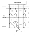
- Fig. 1 illustrates a typical circuit diagram of a TFT panel.
- the TFT panel provides a plurality of display points forming an n ⁇ m matrix with n rows (G1, G2, G3, ..., Gn) and m columns (S1, S2, S3, ...,Sm), wherein each display point represents a Twisted Nematic Liquid Crystal Display (TN-LCD) point and includes a TFT, a parallel plate capacitor (not shown) formed with upper and lower conductive glasses and a storage capacitor, the parallel plate capacitor and storage capacitor having parallel coupling.
- TN-LCD Twisted Nematic Liquid Crystal Display
- a parallel plate capacitor not shown
- a basic pixel display unit needs to be provided with three such display points corresponding to red, green and blue, i.e. the three basic primary colors.
- the gate driver outputs a drive pulse to turn on all TFT's in a row.
- the source driver charges the display points in the row to the necessary voltage.
- the gate driver turns off the TFT's in the row, turns on TFT's in the next row, and charges the display points in the next row.
- Fig. 2 illustrates a circuit diagram of a TFT-LCD driver circuit according to the first embodiment of the present invention.
- the TFT-LCD driver circuit includes gate and source drivers, a grayscale voltage generator with a timing generator (not shown), and a bias voltage generator (not shown).
- TFTs N1-Nm are provided in the row.
- a gate of each of the TFTs is turned on or off under the control of the dirve pulse outputted from the gate driver, m sources of the TFTs are respectively coupled to outputs of source drivers, and m drains of the TFTs are respectively coupled to storage capacitors Cs1-Csm.
- all the TFTs of the row are turned on by the drive pulse outputted from the gate driver.
- latch data stored within the source drive latch is decoded and converted by Digital to Analog Converters (DACs), to select a grayscale voltage generator to generate the grayscale voltage to be supplied to each display point.
- DACs Digital to Analog Converters
- the grayscale voltage is transmitted through the source drive buffer and a corresponding one of the transmission gates T1-Tm to charge a display electrode of the respective display point, thereby driving the LCD panel.
- m source drive buffers (within the dashed outline) corresponds to m display points in the row under scan, and each source drive buffer includes an operational amplifier (OPA).
- OPA operational amplifier
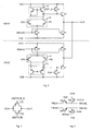
- Fig. 3 illustrates the relationship between input and output signals of the OPA of the source drive buffer as shown in Fig. 2 .
- the OPA receives the voltage signal PIN from the corresponding DAC, latches the voltage signal PIN and charges the corresponding display electrode through the corresponding one of the transmission gates T1-Tm (as shown in Fig. 2 ) under the control of timing signals PDP, PDP_N, PDN, PDN_N and bias voltage signals PBIASL and NBIASL.
- the output OUT of the OPA is short connected to a feedback NIN, causing the output voltage to be fed back to the feedback NIN of the OPA, and the entire OPA is equivalent to a voltage follower.
- the various timing signals are generated by the timing generators of the TFT-LCD driver circuit.
- Fig. 4 is a circuit diagram of the OPA according to an embodiment of the present invention.
- the OPA includes a first differential amplifier (OPAN) and a second differential amplifier (OPAP), which operate alternatively under the control of timing signals.
- the input stage of the OPAN includes a first differential circuit 41 having two N-channel Metal Oxide Semiconductors (NMOSs), and the gates of the NMOSs are coupled to the voltage output PIN of the DAC and the output OUT of the source drive buffer.
- the sources of the two NMOSs can be coupled to each other to form a coupled source pair, and connected with the ground potential VSS of the driver circuit via a first switch Q1.
- the drains of the first differential circuit 41 are coupled to the power terminal VDD of the drive circuit via a first current mirror source 42.
- the output stage of the OPAN is of a simple co-source structure to improve the range of the output waveforms, and is formed with a second switch Q2 and a third switch Q3 coupled in series, and the coupling node between the switches Q2 and Q3 is the output OUT of the OPA.
- the gates of the second switch Q2 and the first switch Q1 are coupled in series, and turned on under the control of the bias voltage signal NBIASL.
- the gate of the third switch Q3 is coupled to the source of the first current mirror source 42, and also to the power terminal VDD of the drive circuit via a fourth switch Q4.
- the gate of the fourth switch Q4 can be turned on under the control of the timing signal PDN_N, to control and ensure that the OPAN is working properly.
- the input stage of the OPAP includes a second differential circuit 43 formed with two P-channel Metal Oxide Semiconductors (PMOSs), and the gates of the two PMOSs are coupled to the voltage output PIN of the DAC and the output OUT of the source drive buffer.
- the sources of the two PMOSs are connected with the power terminal VDD of the drive circuit via a fifth switch Q5.
- the drains of the second differential circuit 43 are coupled to the ground potential VSS of the driver circuit via a second current mirror source 44. With the second current mirror source 44 as the load, the output impedance is improved to obtain a higher gain.
- the output stage of the OPAP is of a simple co-source structure, and includes sixth and seventh switches Q6, Q7 coupled in series, and the coupling node between the switches Q6 and Q7 is the output OUT of the OPA.
- the gates of the sixth switch Q6 and the fifth switch Q5 are coupled in series, and are turned on under the control of the bias voltage control signal PBIASL.
- the gate of the seventh switch Q7 is coupled to the source of the second current mirror source 44, and also to the ground potential VSS of the driver circuit via an eighth switch Q8.
- the gate of the eighth switch Q8 can be turned on under the control of the timing signal PDP, to control the operation status of the OPAP.
- the two differential amplifiers OPAN and OPAP of the OPA as shown in Fig. 4 operate alternatively under the control of the timing signals, with the OPAN being effective when the voltage rises and the OPAP being effective when the voltage decreases.
- the OPA within the buffer can be coupled in parallel to a CMOS transmission gate as shown in Fig. 5 , which adjusts the output waveform.
- the source of the PMOS T51 and the drain of the NMOS T52 can be coupled to form an input of the CMOS transmission gate, while the drain of the PMOS T51 and the source of the NMOS T52 can be coupled to form an output of the CMOS transmission gate. Because the sources and drains of the NMOS and PMOS can be exchanged, other coupling structures may be utilized. For example, the drains of the NMOS and PMOS are coupled and the sources of the NMOS and PMOS are coupled.
- the PMOS T51 and the NMOS T52 can be turned on under the control of a pair of complementary timing signals SWITCH and SWITCH_N.
- the input of the CMOS transmission gate can be coupled to the input PIN of the OPA while the output of the CMOS transmission gate can be connected to the output OUT of the OPA.
- Figs. 6 and 7 respectively illustrate a control circuit diagram and waveforms of the bias voltages PBIASL and NBIASL in the TFT-LCD driver circuit according to an embodiment of the present invention.
- the generator which generates the bias voltage signals PBIASL and NBIASL serves as a global circuit module which provides the bias voltages for all source drive buffers in the TFT-LCD driver circuit, while the other circuit modules in the TFT-LCD driver circuit are provided with bias voltages by the bias voltage signals PBIAS and NBIAS.
- PDP is at a high voltage level while PDP_N is at a low voltage level.
- a switch T62 is on, a switch T61 is off, and the bias voltage signal PBIASL is pulled up to a system high voltage level VDD.
- the PDP is at a low voltage level while the PDP_N is at a high voltage level.
- the switch T61 is on, the switch T62 is off, and the bias voltage signal PBIAS is directly outputted as the bias voltage signal PBIASL.
- the PDN is at a low voltage level while the PDN_N is at a high voltage level.
- a switch T63 is on, a switch T64 is off, and the bias voltage signal NBIAS is directly outputted as the bias voltage signal NBIASL.
- the PDN is at a high voltage level while the PDN_N is at a low voltage level.
- the switch T64 is on, the switch T63 is off, and the bias voltage signal NBIASL is pulled down to a system low voltage level VSS.
- the waveforms of the bias voltage signals PBIASL and NBIASL are shown in Fig. 7
- the waveforms of timing signals SWITCH and SWITCH_N and other timing signals are shown in Fig. 8 .
- the working principles of the source drive buffer according to an embodiment of the present invention during the time for scanning a row i.e. periods tl+t2+t3, are described as follows.
- the data as stored in the source drive latch are decoded and converted by the DAC, to select the grayscale voltage generator to generate the appropriate grayscale voltage.
- the first switch Q1 and the second switch Q2 are turned on by the bias voltage signal NBIASL, and both the first differential circuit 41 and the first current mirror source 42 start to operate. Because the PDN_N is at a high voltage level, the fourth switch Q4 is off, the OPAN is able to function normally, and the voltage generated by the grayscale voltage generator is buffered and outputted.
- the bias voltage signal PBIASL is at a high voltage level
- the fifth switch Q5 is off
- the PDP is at a high voltage level
- the eighth switch Q8 is on, thereby pulling down or lowering the gate voltage of the seventh switch Q7 to the low voltage level VSS, turning off the OPAP. That is, the OPAN is in operation during the period t1.
- the OPAP is operative, the control principle of which is opposite to that during the period t1, and thus will not be elaborated further herein. Because the entire OPA is equivalent to a voltage follower, during the periods t1 and t2, the voltage following approach ensures that the level of the output OUT is equal to the level of the input PIN.
- neither of the bias voltage signals NBIASL and PBIASL can turn on the first and fifth switches Q1 and Q5.
- Both the first and second differential amplifiers OPAN and OPAP are off, in this case, the CMOS transmission gate is turned on under the control of the timing signals SWITCH and SWITCH_N, thereby short connecting the input and output of the source drive buffer, and the output of the source drive buffer is adjusted by the voltage from the DAC and reaches or is close to an ideal value.
- Fig. 9 illustrates waveforms of the voltage generated by the DAC that is buffered and outputted by the source drive buffer according to an embodiment of the present invention under the control of the various timing signals.
- N1 represents the drive pulse waveform outputted from the gate driver
- T1 represents the waveform of the transmission gate as shown in Fig. 2
- PIN represents the output waveform of the DAC
- OUT represents the output waveform of the source drive buffer.
- the first differential amplifier OPAN is effective when the voltage rises, i.e. dominant when the input voltage changes from a low level to a high level
- the second differential amplifier OPAP is effective when the voltage decreases, i.e. dominant when the input voltage changes from a high level to a low level. Therefore, only one differential amplifier is contributing to the system during the time for scanning one row, thereby causing differentiation between the output waveform and the actual input waveform of the buffer.
- the differentiation will not influence the display on the LCD, because the voltage in the storage capacitor Cs of the LCD panel just before the TFT is turned off is stored, that is, the output of the cache has reached or been close to an ideal value when N1 is changed from the higher voltage to the lower voltage.
- the power amplifiers in order to reduce static power consumption of power amplifiers, operate in the sub-threshold zone, and the voltage values of the bias voltage signals PBIAS and NBIAS are slightly lower than the threshold voltage.
- mixed use of an NMOS differential pair (first differential amplifier) and a PMOS differential pair (second differential amplifier) may be incorporated as a two-tier operational amplifier.
- the two operational amplifiers operate in a time division mode through timing control, thereby effectively improving the range of the input voltage.
- circuitry dimensions can be reduced and less area or die size would be required.
- power consumption can also be reduced because the two differential operational amplifiers operate in a time division mode.
Landscapes
- Engineering & Computer Science (AREA)
- Power Engineering (AREA)
- Chemical & Material Sciences (AREA)
- Crystallography & Structural Chemistry (AREA)
- Physics & Mathematics (AREA)
- Computer Hardware Design (AREA)
- General Physics & Mathematics (AREA)
- Theoretical Computer Science (AREA)
- Liquid Crystal Display Device Control (AREA)
- Control Of Indicators Other Than Cathode Ray Tubes (AREA)
- Amplifiers (AREA)
Abstract
Description
- The present invention relates to Liquid Crystal Displays (LCDs), more specifically, to a Thin Film Transistor-Liquid Crystal Display (TFT-LCD) driver circuit and LCD devices.
- Current TFT-LCD technologies have been trending toward higher levels of integration, higher resolution and multi-grayscale capabilities. As such, the TFT-LCD driver circuit device area and power consumption have increased accordingly, leading to higher manufacturing costs. In a traditional TFT-LCD driver circuit, a source drive buffer or latch of the source drive chip occupies a large footprint and consumes a considerable amount of power.
- Thus, chip designers are starting to look into ways of going about reducing the footprint and/or power consumption of the source drive buffer or latch on the source drive chip.
- Accordingly, there is a need for an improved TFT-LCD driver circuit and corresponding LCD devices.
- An object according to an embodiment of the present invention is to eliminate the large area occupation and the high power consumption of the source drive buffer in the traditional TFT-LCD driver circuit. Accordingly, a first embodiment discloses a TFT-LCD driver circuit including: a gate driver adapted to control turning on of a Thin Film Transistor (TFT); a grayscale voltage generation circuit capable of providing a grayscale voltage for display points; a timing circuit configured to provide timing signals; a bias circuit configured to provide bias voltage signals; and a source driver operable to charge the display points according to the grayscale voltage. The source driver includes: a source drive latch configured to store data for the display points; a source drive buffer; and a Digital to Analog Converter (DAC) configured to output the grayscale voltage to the source drive buffer according to the stored display data. The source drive buffer includes an Operational Amplifier (OPA), which includes first and second differential amplifiers, The differential amplifiers operate alternatively according to the timing signals and bias voltage signals, and buffer and output voltage signals outputted from the DAC by means of a voltage follower mechanism for charging the display points.
- The source drive buffer further includes a CMOS transmission gate in parallel with the OPA, and the CMOS transmission gate is capable of adjusting the voltage output of the OPA using output voltage signals outputted from the DAC under the control of the timing signals while the OPA is off.
- The first differential amplifier includes: a first differential circuit having two N-channel Metal Oxide Semiconductor (NMOS), wherein the gate of the first NMOS is coupled to the output of the DAC and the gate of the second NMOS is coupled to the output of the OPA; a first current mirror source being a loader of the first differential circuit; an end of current source; an output stage which includes a NMOS and a PMOS, the gate of the NMOS and the end of current source being controlled by the bias voltage signals, the gate of the PMOS being coupled to the output of the first current mirror source; and a power down PMOS operable to turning on and off the OPA by timing signals.
- The second differential amplifier includes: a second differential circuit having two P-channel Metal Oxide Semiconductor (PMOS), wherein the gate of the first PMOS is coupled to the output of the DAC while the gate of the second PMOS is coupled to the output of the OPA; a second current mirror source being a loader of the second differential circuit; an end of current source; an output stage which includes a PMOS and a NMOS, the gate of the PMOS and the end of current source being controlled by the bias voltage signals, the gate of the NMOS being coupled to the output of the second current mirror source; and a power down NMOS which is applied for turning on and off OPA by timing signals.
- In an embodiment, during sub-threshold zone, the threshold voltage of the OPA is higher than the bias voltage signals generated by the bias circuit.
- In an embodiment, an LCD device can be manufactured having a TFT panel and using the TFT-LCD driver circuit as described above.
- Other variations, embodiments and features of the present invention will become evident from the following detailed description, drawings and claims.
-
-
Fig. 1 illustrates a typical circuit diagram of a TFT panel; -
Fig. 2 illustrates a schematic diagram of the TFT-LCD driver circuit according to a first embodiment of the present invention; -
Fig. 3 illustrates the relationship between input and output signals of an OPA of a source drive buffer ofFig. 2 ; -
Fig. 4 illustrates a circuit diagram of the OPA according to an embodiment of the present invention; -
Fig. 5 illustrates a circuit diagram of a CMOS transmission gate of the source drive buffer according to an embodiment of the present invention; -
Fig. 6 illustrates a diagram of a control circuit for bias voltages PBIASL and NBIASL of the TFT-LCD driver circuit according to an embodiment of the present invention; -
Fig. 7 illustrates waveforms of the bias voltages PBIASL and NBIASL of the TFT-LCD driver circuit according to an embodiment of the present invention; -
Fig. 8 illustrates waveforms of timing signals SWITCH and SWITCH_N and some other timing signals of the source driver according to an embodiment of the present invention; and -
Fig. 9 illustrates waveforms of the voltage generated by the DAC that is buffered and outputted by the source drive buffer according to an embodiment of the present invention under the control of the various timing signals. - It will be appreciated by those of ordinary skill in the art that the invention can be embodied in other specific forms without departing from the essential characteristics thereof. The presently disclosed embodiments are therefore considered in all respects to be illustrative but not restrictive.
- The source drive buffer of the TFT-LCD driver circuit of the presently disclosed embodiments can be formed with two basic differential amplifiers and a CMOS transmission gate. The two differential amplifiers can be turned on alternatively according to timing of control signals, adjust an output voltage through the COMS transmission gate, and charge pixels in a row to the required voltage level until scanning of the pixels in the row is completed.
-
Fig. 1 illustrates a typical circuit diagram of a TFT panel. The TFT panel provides a plurality of display points forming an n×m matrix with n rows (G1, G2, G3, ..., Gn) and m columns (S1, S2, S3, ...,Sm), wherein each display point represents a Twisted Nematic Liquid Crystal Display (TN-LCD) point and includes a TFT, a parallel plate capacitor (not shown) formed with upper and lower conductive glasses and a storage capacitor, the parallel plate capacitor and storage capacitor having parallel coupling. If a color filter has three basic colors, a basic pixel display unit needs to be provided with three such display points corresponding to red, green and blue, i.e. the three basic primary colors. At a specific time, the gate driver outputs a drive pulse to turn on all TFT's in a row. At the same time, the source driver charges the display points in the row to the necessary voltage. When the charging of the row is completed, the gate driver turns off the TFT's in the row, turns on TFT's in the next row, and charges the display points in the next row. -
Fig. 2 illustrates a circuit diagram of a TFT-LCD driver circuit according to the first embodiment of the present invention. For the sake of description, only TFT-components of the LCD driver circuit involved in the invention are shown inFigure 2 . The TFT-LCD driver circuit includes gate and source drivers, a grayscale voltage generator with a timing generator (not shown), and a bias voltage generator (not shown). - As shown in
Fig. 2 , TFTs N1-Nm are provided in the row. A gate of each of the TFTs is turned on or off under the control of the dirve pulse outputted from the gate driver, m sources of the TFTs are respectively coupled to outputs of source drivers, and m drains of the TFTs are respectively coupled to storage capacitors Cs1-Csm. When the row is canned, all the TFTs of the row are turned on by the drive pulse outputted from the gate driver. At the same time, latch data stored within the source drive latch is decoded and converted by Digital to Analog Converters (DACs), to select a grayscale voltage generator to generate the grayscale voltage to be supplied to each display point. The grayscale voltage is transmitted through the source drive buffer and a corresponding one of the transmission gates T1-Tm to charge a display electrode of the respective display point, thereby driving the LCD panel. As shown inFig. 2 , m source drive buffers (within the dashed outline) corresponds to m display points in the row under scan, and each source drive buffer includes an operational amplifier (OPA). -
Fig. 3 illustrates the relationship between input and output signals of the OPA of the source drive buffer as shown inFig. 2 . Specifically, the OPA receives the voltage signal PIN from the corresponding DAC, latches the voltage signal PIN and charges the corresponding display electrode through the corresponding one of the transmission gates T1-Tm (as shown inFig. 2 ) under the control of timing signals PDP, PDP_N, PDN, PDN_N and bias voltage signals PBIASL and NBIASL. The output OUT of the OPA is short connected to a feedback NIN, causing the output voltage to be fed back to the feedback NIN of the OPA, and the entire OPA is equivalent to a voltage follower. The various timing signals are generated by the timing generators of the TFT-LCD driver circuit. -
Fig. 4 is a circuit diagram of the OPA according to an embodiment of the present invention. The OPA includes a first differential amplifier (OPAN) and a second differential amplifier (OPAP), which operate alternatively under the control of timing signals. The input stage of the OPAN includes a firstdifferential circuit 41 having two N-channel Metal Oxide Semiconductors (NMOSs), and the gates of the NMOSs are coupled to the voltage output PIN of the DAC and the output OUT of the source drive buffer. The sources of the two NMOSs can be coupled to each other to form a coupled source pair, and connected with the ground potential VSS of the driver circuit via a first switch Q1. Depending on the bias at the first switch Q1, the drains of the firstdifferential circuit 41 are coupled to the power terminal VDD of the drive circuit via a firstcurrent mirror source 42. With the firstcurrent mirror source 42 as the load, the output impedance is improved to obtain a higher gain. The output stage of the OPAN is of a simple co-source structure to improve the range of the output waveforms, and is formed with a second switch Q2 and a third switch Q3 coupled in series, and the coupling node between the switches Q2 and Q3 is the output OUT of the OPA. The gates of the second switch Q2 and the first switch Q1 are coupled in series, and turned on under the control of the bias voltage signal NBIASL. The gate of the third switch Q3 is coupled to the source of the firstcurrent mirror source 42, and also to the power terminal VDD of the drive circuit via a fourth switch Q4. The gate of the fourth switch Q4 can be turned on under the control of the timing signal PDN_N, to control and ensure that the OPAN is working properly. - Similarly, the input stage of the OPAP includes a second
differential circuit 43 formed with two P-channel Metal Oxide Semiconductors (PMOSs), and the gates of the two PMOSs are coupled to the voltage output PIN of the DAC and the output OUT of the source drive buffer. The sources of the two PMOSs are connected with the power terminal VDD of the drive circuit via a fifth switch Q5. Depending on the bias at the fifth switch Q5, the drains of the seconddifferential circuit 43 are coupled to the ground potential VSS of the driver circuit via a secondcurrent mirror source 44. With the secondcurrent mirror source 44 as the load, the output impedance is improved to obtain a higher gain. The output stage of the OPAP is of a simple co-source structure, and includes sixth and seventh switches Q6, Q7 coupled in series, and the coupling node between the switches Q6 and Q7 is the output OUT of the OPA. The gates of the sixth switch Q6 and the fifth switch Q5 are coupled in series, and are turned on under the control of the bias voltage control signal PBIASL. The gate of the seventh switch Q7 is coupled to the source of the secondcurrent mirror source 44, and also to the ground potential VSS of the driver circuit via an eighth switch Q8. The gate of the eighth switch Q8 can be turned on under the control of the timing signal PDP, to control the operation status of the OPAP. - The two differential amplifiers OPAN and OPAP of the OPA as shown in
Fig. 4 operate alternatively under the control of the timing signals, with the OPAN being effective when the voltage rises and the OPAP being effective when the voltage decreases. During the scanning of a row, there is only one contribution from the OPA, which in turn causes differentiation between the output waveform and actual input waveform of the buffer. Accordingly, in one preferred embodiment of the present invention, the OPA within the buffer can be coupled in parallel to a CMOS transmission gate as shown inFig. 5 , which adjusts the output waveform. The source of the PMOS T51 and the drain of the NMOS T52 can be coupled to form an input of the CMOS transmission gate, while the drain of the PMOS T51 and the source of the NMOS T52 can be coupled to form an output of the CMOS transmission gate. Because the sources and drains of the NMOS and PMOS can be exchanged, other coupling structures may be utilized. For example, the drains of the NMOS and PMOS are coupled and the sources of the NMOS and PMOS are coupled. The PMOS T51 and the NMOS T52 can be turned on under the control of a pair of complementary timing signals SWITCH and SWITCH_N. The input of the CMOS transmission gate can be coupled to the input PIN of the OPA while the output of the CMOS transmission gate can be connected to the output OUT of the OPA. -
Figs. 6 and7 respectively illustrate a control circuit diagram and waveforms of the bias voltages PBIASL and NBIASL in the TFT-LCD driver circuit according to an embodiment of the present invention. The generator which generates the bias voltage signals PBIASL and NBIASL serves as a global circuit module which provides the bias voltages for all source drive buffers in the TFT-LCD driver circuit, while the other circuit modules in the TFT-LCD driver circuit are provided with bias voltages by the bias voltage signals PBIAS and NBIAS. - As shown in
Figs. 6 and7 , during periods t1 and t3 within a cycle of gate scanning a row, PDP is at a high voltage level while PDP_N is at a low voltage level. In this case, a switch T62 is on, a switch T61 is off, and the bias voltage signal PBIASL is pulled up to a system high voltage level VDD. During period t2, the PDP is at a low voltage level while the PDP_N is at a high voltage level. In this case, the switch T61 is on, the switch T62 is off, and the bias voltage signal PBIAS is directly outputted as the bias voltage signal PBIASL. Similarly, during the period t1, the PDN is at a low voltage level while the PDN_N is at a high voltage level. In this case, a switch T63 is on, a switch T64 is off, and the bias voltage signal NBIAS is directly outputted as the bias voltage signal NBIASL. During the periods t2 and t3, the PDN is at a high voltage level while the PDN_N is at a low voltage level. In this case, the switch T64 is on, the switch T63 is off, and the bias voltage signal NBIASL is pulled down to a system low voltage level VSS. The waveforms of the bias voltage signals PBIASL and NBIASL are shown inFig. 7 , while the waveforms of timing signals SWITCH and SWITCH_N and other timing signals are shown inFig. 8 . - With reference to
Figs. 2-8 , the working principles of the source drive buffer according to an embodiment of the present invention during the time for scanning a row, i.e. periods tl+t2+t3, are described as follows. The data as stored in the source drive latch are decoded and converted by the DAC, to select the grayscale voltage generator to generate the appropriate grayscale voltage. During period t1, the first switch Q1 and the second switch Q2 are turned on by the bias voltage signal NBIASL, and both the firstdifferential circuit 41 and the firstcurrent mirror source 42 start to operate. Because the PDN_N is at a high voltage level, the fourth switch Q4 is off, the OPAN is able to function normally, and the voltage generated by the grayscale voltage generator is buffered and outputted. Further, because the bias voltage signal PBIASL is at a high voltage level, the fifth switch Q5 is off, and because the PDP is at a high voltage level, the eighth switch Q8 is on, thereby pulling down or lowering the gate voltage of the seventh switch Q7 to the low voltage level VSS, turning off the OPAP. That is, the OPAN is in operation during the period t1. During the period t2, the OPAP is operative, the control principle of which is opposite to that during the period t1, and thus will not be elaborated further herein. Because the entire OPA is equivalent to a voltage follower, during the periods t1 and t2, the voltage following approach ensures that the level of the output OUT is equal to the level of the input PIN. It should be appreciated by one skilled in the art that the previously described scenario may be reversed by means of timing control such that the OPAP is in operation during period t1 while the OPAN is in operation during period t2. The operational functions of the amplifiers and corresponding grayscale voltages are similar to those described above and thus will not be elaborated further herein. - During period t3, neither of the bias voltage signals NBIASL and PBIASL can turn on the first and fifth switches Q1 and Q5. Both the first and second differential amplifiers OPAN and OPAP are off, in this case, the CMOS transmission gate is turned on under the control of the timing signals SWITCH and SWITCH_N, thereby short connecting the input and output of the source drive buffer, and the output of the source drive buffer is adjusted by the voltage from the DAC and reaches or is close to an ideal value.
-
Fig. 9 illustrates waveforms of the voltage generated by the DAC that is buffered and outputted by the source drive buffer according to an embodiment of the present invention under the control of the various timing signals. Specifically, N1 represents the drive pulse waveform outputted from the gate driver, T1 represents the waveform of the transmission gate as shown inFig. 2 , PIN represents the output waveform of the DAC, and OUT represents the output waveform of the source drive buffer. - In the embodiments described above, the first differential amplifier OPAN is effective when the voltage rises, i.e. dominant when the input voltage changes from a low level to a high level, while the second differential amplifier OPAP is effective when the voltage decreases, i.e. dominant when the input voltage changes from a high level to a low level. Therefore, only one differential amplifier is contributing to the system during the time for scanning one row, thereby causing differentiation between the output waveform and the actual input waveform of the buffer. However, after adjustments by the grayscale voltage, the differentiation will not influence the display on the LCD, because the voltage in the storage capacitor Cs of the LCD panel just before the TFT is turned off is stored, that is, the output of the cache has reached or been close to an ideal value when N1 is changed from the higher voltage to the lower voltage.
- The presently disclosed embodiments, in order to reduce static power consumption of power amplifiers, the power amplifiers operate in the sub-threshold zone, and the voltage values of the bias voltage signals PBIAS and NBIAS are slightly lower than the threshold voltage.
- Additionally, to expand the range of the common-mode input, mixed use of an NMOS differential pair (first differential amplifier) and a PMOS differential pair (second differential amplifier) may be incorporated as a two-tier operational amplifier. The two operational amplifiers operate in a time division mode through timing control, thereby effectively improving the range of the input voltage. Further, because of the reduced complexity of the source drive buffer, circuitry dimensions can be reduced and less area or die size would be required. Furthermore, power consumption can also be reduced because the two differential operational amplifiers operate in a time division mode.
- Although the invention has been described in detail with reference to several embodiments, additional variations and modifications exist within the scope of the invention as described and defined in the following claims.
Claims (13)
- A Thin Film Transistor-Liquid Crystal Display, TFT-LCD, driver circuit comprising:a gate driver adapted to control turning on of a TFT; a grayscale voltage generation circuit adapted to provide a grayscale voltage for display points;a timing circuit configured to provide a plurality of timing signals;a bias circuit configured to provide a plurality of bias voltage signals; anda source driver operable to charge the display points according to the grayscale voltage, wherein the source driver comprises:wherein, the source drive buffer comprises an operational amplifier, which comprises a first differential amplifier and a second differential amplifier, the first and second differential amplifiers operate alternatively according to the timing signals and the bias voltage signals, to buffer and output voltage signals outputted from the DAC in a voltage follower mechanism for charging the display points.a source drive latch configured to store data for display points;a source drive buffer; anda Digital to Analog Converter, DAC, configured to output the grayscale voltage to the source drive buffer according to the stored data;
- The circuit of claim 1, wherein the source drive buffer further comprises a CMOS transmission gate in parallel with the operational amplifier, and when the operational amplifier is off, the CMOS transmission gate adjusts the voltage output of the operational amplifier using the voltage signals outputted from the DAC under the control of the timing signals.
- The circuit of claim 1, wherein the first differential amplifier comprises:a first differential circuit having two N-channel Metal Oxide Semiconductor, NMOS, wherein a gate of the first NMOS is coupled to the output of the DAC and a gate of the second NMOS is coupled to the output of the operational amplifier;a first current mirror source being a loader of the first differential circuit;an end of current source;an output stage which comprises a NMOS and a PMOS, the gate of the NMOS and the end of current source being controlled by the bias voltage signals, the gate of the PMOS being coupled to the output of the first current mirror source; anda power down PMOS operable to turning on and off the operational amplifier by timing signals.
- The circuit of claim 1, wherein the second differential amplifier comprises:a second differential circuit having two P-channel Metal Oxide Semiconductor, PMOS, wherein a gate of the first PMOS is coupled to the output of the DAC while a gate of the second PMOS is coupled to the output of the operational amplifier;a second current mirror source being a loader of the second differential circuit;an end of current source;an output stage which comprises a PMOS and a NMOS, the gate of the PMOS and the end of current source being controlled by the bias voltage signals, the gate of the NMOS being coupled to the output of the second current mirror source; anda power down NMOS which is applied for turning on and off operational amplifier by timing signals.
- The circuit of any one of claims 1 to 4, wherein the operational amplifier operates in a sub-threshold zone, and the threshold voltage of the operational amplifier is higher than the bias voltage signals generated by the bias circuit.
- A Liquid Crystal Display, LCD, device comprising:a Thin Film Transistor, TFT, panel; anda TFT-LCD driver circuit comprising:wherein, the source drive buffer comprises an operational amplifier, which comprises a first differential amplifier and a second differential amplifier, the first and second differential amplifiers operate alternatively according to the timing signals and the bias voltage signals, to buffer and output voltage signals outputted from the DAC in a voltage follower mechanism for charging the display points.a gate driver adapted to control turning on of a TFT; a grayscale voltage generation circuit adapted to provide a grayscale voltage for display points;a timing circuit configured to provide a plurality of timing signals;a bias circuit configured to provide a plurality of bias voltage signals; anda source driver operable to charge the display points according to the grayscale voltage, wherein the source driver comprises:a source drive latch configured to store data for display points;a source drive buffer; anda Digital to Analog Converter, DAC, configured to output the grayscale voltage to the source drive buffer according to the stored data;
- The device of claim 6, wherein the source drive buffer further comprises a CMOS transmission gate in parallel with the operational amplifier, and when the operational amplifier is off, the CMOS transmission gate adjusts the voltage output of the operational amplifier using the voltage signals outputted from the DAC under the control of the timing signals.
- The device of claim 6, wherein the first differential amplifier comprises:a first differential circuit having two N-channel Metal Oxide Semiconductor, NMOS, wherein a gate of the first NMOS is coupled to the output of the DAC and a gate of the second NMOS is coupled to the output of the operational amplifier;a first current mirror source being a loader of the first differential circuit;an end of current source;an output stage which comprises a NMOS and a PMOS, the gate of the NMOS and the end of current source being controlled by the bias voltage signals, the gate of the PMOS being coupled to the output of the first current mirror source; anda power down PMOS operable to turning on and off the operational amplifier by timing signals.
- The device of claim 6, wherein the second differential amplifier comprises:a second differential circuit having two P-channel Metal Oxide Semiconductor, PMOS, wherein a gate of the first PMOS is coupled to the output of the DAC while a gate of the second PMOS is coupled to the output of the operational amplifier;a second current mirror source being a loader of the second differential circuit;an end of current source;an output stage which comprises a PMOS and a NMOS, the gate of the PMOS and the end of current source being controlled by the bias voltage signals, the gate of the NMOS being coupled to the output of the second current mirror source; anda power down NMOS which is applied for turning on and off operational amplifier by timing signals.
- The device of any one of claims 6 to 9, wherein the operational amplifier operates in a sub-threshold zone, and the threshold voltage of the operational amplifier is higher than the bias voltage signals generated by the bias circuit.
- A Thin Film Transistor-Liquid Crystal Display, TFT-LCD, driver circuit comprising:a gate driver adapted to control turning on of a TFT; a grayscale voltage generation circuit adapted to provide a grayscale voltage for display points;a timing circuit configured to provide a plurality of timing signals;a bias circuit configured to provide a plurality of bias voltage signals; anda source driver operable to charge the display points according to the grayscale voltage, wherein the source driver comprises:wherein, the source drive buffer comprises an operational amplifier, the operational amplifier having:a source drive latch configured to store data for display points;a source drive buffer; anda digital to analog converter, DAC, configured to output the grayscale voltage to the source drive buffer according to the stored data;a first differential amplifier comprising:wherein the two differential amplifiers operate alternatively according to the timing signals and the bias voltage signals, to buffer and output voltage signals outputted from the DAC in a voltage follower mechanism for charging the display points.a first differential circuit having two N-channel Metal Oxide Semiconductor, NMOS, wherein a gate of the first NMOS is coupled to the output of the DAC and a gate of the second NMOS is coupled to the output of the operational amplifier;a first current mirror source being a loader of the first differential circuit;a first end of current source;an output stage which comprises a third NMOS and a third PMOS, the gate of the third NMOS and the first end of current source controlled by the bias voltage signals, the gate of the third PMOS coupled to the output of the first current mirror source;a power down PMOS operable to turning on and off the operational amplifier by timing signals;a second differential amplifier comprising:a second differential circuit having two P-channel Metal Oxide Semiconductor, PMOS, wherein a gate of the first PMOS is coupled to the output of the DAC while a gate of the second PMOS is coupled to the output of the operational amplifier;a second current mirror source being a loader of the second differential circuit;a second end of current source;an output stage which comprises a fourth PMOS and a fourth NMOS, the gate of the fourth PMOS and the end of current source controlled by the bias voltage signals, the gate of the fourth NMOS coupled to the output of the second current mirror source;a power down NMOS which is applied for turning on and off operational amplifier by timing signals; and
- The circuit of claim 11, wherein the source drive buffer further comprises a CMOS transmission gate in parallel with the operational amplifier, and when the operational amplifier is off, the CMOS transmission gate adjusts the voltage output of the operational amplifier using the voltage signals outputted from the DAC under the control of the timing signals.
- The circuit of claim 11, wherein the operational amplifier operates in a sub-threshold zone, and the threshold voltage of the operational amplifier is higher than the bias voltage signals generated by the bias circuit.
Applications Claiming Priority (1)
| Application Number | Priority Date | Filing Date | Title |
|---|---|---|---|
| CN2007103058381A CN101471048B (en) | 2007-12-27 | 2007-12-27 | TFT-LCD driving circuit and LCD device |
Publications (2)
| Publication Number | Publication Date |
|---|---|
| EP2075790A2 true EP2075790A2 (en) | 2009-07-01 |
| EP2075790A3 EP2075790A3 (en) | 2009-12-16 |
Family
ID=40466851
Family Applications (1)
| Application Number | Title | Priority Date | Filing Date |
|---|---|---|---|
| EP08400059A Withdrawn EP2075790A3 (en) | 2007-12-27 | 2008-12-23 | TFT-LCD driver circuit and LCD devices |
Country Status (3)
| Country | Link |
|---|---|
| US (1) | US20090167747A1 (en) |
| EP (1) | EP2075790A3 (en) |
| CN (1) | CN101471048B (en) |
Cited By (1)
| Publication number | Priority date | Publication date | Assignee | Title |
|---|---|---|---|---|
| EP2458581B1 (en) * | 2010-11-29 | 2017-02-15 | Optrex Corporation | Drive device for liquid crystal display panel |
Families Citing this family (27)
| Publication number | Priority date | Publication date | Assignee | Title |
|---|---|---|---|---|
| CN101471577B (en) | 2007-12-29 | 2011-06-15 | 比亚迪股份有限公司 | Voltage balance circuit for double-burl chargeable battery |
| CN101471602B (en) | 2007-12-29 | 2012-11-07 | 比亚迪股份有限公司 | Bidirectional DC power supply circuit |
| US8212762B2 (en) * | 2009-10-13 | 2012-07-03 | Himax Technologies Limited | Output amplifier of a source driver with an amplifier circuit having an inverted and non-inverted output |
| US8466908B2 (en) * | 2010-07-13 | 2013-06-18 | Himax Technologies Limited | Display device having a bias control unit for dynamically biasing a buffer and method thereof |
| JP5581957B2 (en) * | 2010-10-08 | 2014-09-03 | ソニー株式会社 | Level conversion circuit, display device, and electronic device |
| CN102571004A (en) * | 2010-12-27 | 2012-07-11 | 无锡华润上华半导体有限公司 | Operational amplifier |
| US9373297B2 (en) | 2011-09-16 | 2016-06-21 | Kopin Corporation | Power saving drive mode for bi-level video |
| CN102386861B (en) * | 2011-11-07 | 2015-04-29 | 旭曜科技股份有限公司 | Positive and Negative Input Operational Amplifier Bank |
| TWI474301B (en) * | 2012-07-23 | 2015-02-21 | Au Optronics Corp | Source driver, operating method thereof and display apparatus using the same |
| US8947281B1 (en) * | 2013-03-15 | 2015-02-03 | Clariphy Communications, Inc. | Apparatus and methods for actively terminated digital-to-analog conversion |
| CN104867467A (en) * | 2015-05-26 | 2015-08-26 | 徐新权 | Pixel circuit composed of CMOS transmission gate and plate condenser |
| CN104991876B (en) * | 2015-06-19 | 2018-11-09 | 福建星网锐捷网络有限公司 | A kind of serial bus control method and device |
| CN106340265B (en) * | 2015-07-14 | 2019-03-12 | 上海和辉光电有限公司 | Display panel, source electrode driver and operational amplifier |
| CN105096862B (en) * | 2015-08-04 | 2017-11-17 | 深圳市华星光电技术有限公司 | Source drives chip drive circuit and liquid crystal display panel |
| CN106725427B (en) * | 2016-12-16 | 2024-05-14 | 东莞广州中医药大学中医药数理工程研究院 | Multi-conductive electrocardio electrode connecting device |
| CN106877830B (en) * | 2017-04-06 | 2023-05-02 | 上海芯问科技有限公司 | Analog front-end circuit for detecting physiological potential signals |
| CN107425836A (en) * | 2017-08-16 | 2017-12-01 | 上海绘润实业有限公司 | A kind of mosfet driver |
| CN108053799A (en) * | 2018-01-23 | 2018-05-18 | 深圳市华星光电技术有限公司 | Amplifying circuit, source electrode driver and liquid crystal display |
| KR102549888B1 (en) * | 2018-02-08 | 2023-07-03 | 삼성디스플레이 주식회사 | Method of operating a display device supporting a normal mode and a variable frame mode, and the display device |
| US10810922B2 (en) * | 2018-02-22 | 2020-10-20 | Synaptics Incorporated | Device and method for driving display panel |
| JP2019144548A (en) * | 2018-02-22 | 2019-08-29 | シナプティクス インコーポレイテッド | Display driver, display device, and method for driving display panel |
| CN109557143B (en) * | 2018-10-30 | 2020-05-05 | 电子科技大学 | Capacitive humidity sensor interface circuit |
| US11257414B2 (en) * | 2019-06-27 | 2022-02-22 | Synaptics Incorporated | Method and system for stabilizing a source output voltage for a display panel |
| CN115208380A (en) * | 2022-06-27 | 2022-10-18 | 深圳市国微电子有限公司 | Channel selection circuit, clock driver and electronic equipment |
| CN115472131B (en) * | 2022-08-26 | 2024-03-22 | 苇创微电子(上海)有限公司 | Electric balance method of display device source electrode driving circuit and source electrode driving circuit thereof |
| CN116755502B (en) * | 2023-08-17 | 2023-10-20 | 深圳奥简科技有限公司 | Source follower driving circuit, electronic circuit and electronic equipment |
| CN117294298B (en) * | 2023-09-19 | 2024-07-02 | 苏州纳芯微电子股份有限公司 | Buffer circuit and driving device |
Citations (1)
| Publication number | Priority date | Publication date | Assignee | Title |
|---|---|---|---|---|
| EP1265216A2 (en) * | 2001-06-04 | 2002-12-11 | Seiko Epson Corporation | Operational amplifier circuit, driving circuit and driving method |
Family Cites Families (12)
| Publication number | Priority date | Publication date | Assignee | Title |
|---|---|---|---|---|
| US6157360A (en) * | 1997-03-11 | 2000-12-05 | Silicon Image, Inc. | System and method for driving columns of an active matrix display |
| JP3700558B2 (en) * | 2000-08-10 | 2005-09-28 | 日本電気株式会社 | Driving circuit |
| DE10303427A1 (en) * | 2002-02-06 | 2003-10-16 | Nec Corp Tokio Tokyo | Amplifier circuit, driver circuit for a display device, portable telephone and portable electronic device |
| JP3776890B2 (en) * | 2003-02-12 | 2006-05-17 | 日本電気株式会社 | Display device drive circuit |
| JP4207865B2 (en) * | 2004-08-10 | 2009-01-14 | セイコーエプソン株式会社 | Impedance conversion circuit, drive circuit, and control method |
| JP4400403B2 (en) * | 2004-10-06 | 2010-01-20 | セイコーエプソン株式会社 | Power supply circuit, display driver, electro-optical device, and electronic device |
| JP4472507B2 (en) * | 2004-12-16 | 2010-06-02 | 日本電気株式会社 | DIFFERENTIAL AMPLIFIER, DATA DRIVER OF DISPLAY DEVICE USING SAME, AND METHOD FOR CONTROLLING DIFFERENTIAL AMPLIFIER |
| TWI295050B (en) * | 2005-03-15 | 2008-03-21 | Himax Display Inc | Circuit and method for driving display panel |
| US20070290979A1 (en) * | 2006-06-15 | 2007-12-20 | Solomon Systech Limited | Source drive amplifier for flat panel display |
| JP2008122567A (en) * | 2006-11-10 | 2008-05-29 | Nec Electronics Corp | Data driver and display apparatus |
| CN101471577B (en) * | 2007-12-29 | 2011-06-15 | 比亚迪股份有限公司 | Voltage balance circuit for double-burl chargeable battery |
| CN101471602B (en) * | 2007-12-29 | 2012-11-07 | 比亚迪股份有限公司 | Bidirectional DC power supply circuit |
-
2007
- 2007-12-27 CN CN2007103058381A patent/CN101471048B/en not_active Expired - Fee Related
-
2008
- 2008-12-01 US US12/325,331 patent/US20090167747A1/en not_active Abandoned
- 2008-12-23 EP EP08400059A patent/EP2075790A3/en not_active Withdrawn
Patent Citations (1)
| Publication number | Priority date | Publication date | Assignee | Title |
|---|---|---|---|---|
| EP1265216A2 (en) * | 2001-06-04 | 2002-12-11 | Seiko Epson Corporation | Operational amplifier circuit, driving circuit and driving method |
Cited By (1)
| Publication number | Priority date | Publication date | Assignee | Title |
|---|---|---|---|---|
| EP2458581B1 (en) * | 2010-11-29 | 2017-02-15 | Optrex Corporation | Drive device for liquid crystal display panel |
Also Published As
| Publication number | Publication date |
|---|---|
| EP2075790A3 (en) | 2009-12-16 |
| CN101471048A (en) | 2009-07-01 |
| CN101471048B (en) | 2011-04-20 |
| US20090167747A1 (en) | 2009-07-02 |
Similar Documents
| Publication | Publication Date | Title |
|---|---|---|
| US8988402B2 (en) | Output circuit, data driver, and display device | |
| CN101471048B (en) | TFT-LCD driving circuit and LCD device | |
| US8390609B2 (en) | Differential amplifier and drive circuit of display device using the same | |
| US8274504B2 (en) | Output amplifier circuit and data driver of display device using the same | |
| US10255847B2 (en) | Level shift circuit and display driver | |
| US6567327B2 (en) | Driving circuit, charge/discharge circuit and the like | |
| CN101174397B (en) | Data driver and display device | |
| CN108091307B (en) | Output circuit and data driver of liquid crystal display device | |
| US7656419B2 (en) | Drive circuit for display apparatus and display apparatus | |
| US20110242145A1 (en) | Display device, differential amplifier, and data line drive method for display device | |
| US9269321B2 (en) | Display panel source line driving circuitry | |
| JP5442558B2 (en) | Output circuit, data driver, and display device | |
| US20070290983A1 (en) | Output circuit of a source driver, and method of outputting data in a source driver | |
| US7554389B2 (en) | Differential amplifier and digital-to-analog converter | |
| WO2010050543A1 (en) | Level shifter circuit, load-driving device, and liquid crystal display device | |
| CN101504867A (en) | Level shift circuit, and driver and display system using the same | |
| JP2008122567A (en) | Data driver and display apparatus | |
| US7116171B2 (en) | Operational amplifier and driver circuit using the same | |
| EP4141855B1 (en) | Shift register unit and driving method therefor, gate drive circuit and display device | |
| US12198654B2 (en) | Output amplifier, source driver, and display apparatus | |
| KR100908654B1 (en) | Level shifter and latch with built-in | |
| US7221194B2 (en) | Analog buffers composed of thin film transistors | |
| US8310428B2 (en) | Display panel driving voltage output circuit | |
| JP3228411B2 (en) | Drive circuit for liquid crystal display | |
| KR101227342B1 (en) | Semiconductor integrated circuit device and liquid crystal display driving semiconductor integrated circuit device |
Legal Events
| Date | Code | Title | Description |
|---|---|---|---|
| PUAI | Public reference made under article 153(3) epc to a published international application that has entered the european phase |
Free format text: ORIGINAL CODE: 0009012 |
|
| AK | Designated contracting states |
Kind code of ref document: A2 Designated state(s): AT BE BG CH CY CZ DE DK EE ES FI FR GB GR HR HU IE IS IT LI LT LU LV MC MT NL NO PL PT RO SE SI SK TR |
|
| AX | Request for extension of the european patent |
Extension state: AL BA MK RS |
|
| PUAL | Search report despatched |
Free format text: ORIGINAL CODE: 0009013 |
|
| AK | Designated contracting states |
Kind code of ref document: A3 Designated state(s): AT BE BG CH CY CZ DE DK EE ES FI FR GB GR HR HU IE IS IT LI LT LU LV MC MT NL NO PL PT RO SE SI SK TR |
|
| AX | Request for extension of the european patent |
Extension state: AL BA MK RS |
|
| 17P | Request for examination filed |
Effective date: 20100316 |
|
| 17Q | First examination report despatched |
Effective date: 20100723 |
|
| AKX | Designation fees paid |
Designated state(s): AT BE BG CH CY CZ DE DK EE ES FI FR GB GR HR HU IE IS IT LI LT LU LV MC MT NL NO PL PT RO SE SI SK TR |
|
| STAA | Information on the status of an ep patent application or granted ep patent |
Free format text: STATUS: THE APPLICATION IS DEEMED TO BE WITHDRAWN |
|
| 18D | Application deemed to be withdrawn |
Effective date: 20120221 |