EP2075708B1 - Communication system between independently clocked devices - Google Patents
Communication system between independently clocked devices Download PDFInfo
- Publication number
- EP2075708B1 EP2075708B1 EP08022446A EP08022446A EP2075708B1 EP 2075708 B1 EP2075708 B1 EP 2075708B1 EP 08022446 A EP08022446 A EP 08022446A EP 08022446 A EP08022446 A EP 08022446A EP 2075708 B1 EP2075708 B1 EP 2075708B1
- Authority
- EP
- European Patent Office
- Prior art keywords
- terminal
- receiving
- datum
- communication system
- receiving terminal
- Prior art date
- Legal status (The legal status is an assumption and is not a legal conclusion. Google has not performed a legal analysis and makes no representation as to the accuracy of the status listed.)
- Active
Links
- 238000004891 communication Methods 0.000 title claims description 60
- 230000001360 synchronised effect Effects 0.000 claims description 80
- 239000013256 coordination polymer Substances 0.000 claims description 46
- 230000005540 biological transmission Effects 0.000 claims description 34
- 239000003990 capacitor Substances 0.000 claims description 14
- 238000000034 method Methods 0.000 claims description 13
- 230000002596 correlated effect Effects 0.000 claims description 7
- 230000002457 bidirectional effect Effects 0.000 claims description 6
- 230000015556 catabolic process Effects 0.000 claims description 5
- 238000006731 degradation reaction Methods 0.000 claims description 5
- 238000005192 partition Methods 0.000 claims description 5
- 238000011156 evaluation Methods 0.000 claims description 4
- 238000003860 storage Methods 0.000 claims description 4
- 238000004519 manufacturing process Methods 0.000 claims description 3
- 238000005516 engineering process Methods 0.000 description 5
- 230000008901 benefit Effects 0.000 description 3
- 230000010354 integration Effects 0.000 description 3
- 230000008054 signal transmission Effects 0.000 description 3
- XUIMIQQOPSSXEZ-UHFFFAOYSA-N Silicon Chemical compound [Si] XUIMIQQOPSSXEZ-UHFFFAOYSA-N 0.000 description 2
- 238000013459 approach Methods 0.000 description 2
- 238000013461 design Methods 0.000 description 2
- 230000008569 process Effects 0.000 description 2
- 230000000630 rising effect Effects 0.000 description 2
- 230000000295 complement effect Effects 0.000 description 1
- 230000000875 corresponding effect Effects 0.000 description 1
- 230000008878 coupling Effects 0.000 description 1
- 238000010168 coupling process Methods 0.000 description 1
- 238000005859 coupling reaction Methods 0.000 description 1
- 230000003111 delayed effect Effects 0.000 description 1
- 238000001514 detection method Methods 0.000 description 1
- 238000011161 development Methods 0.000 description 1
- 238000009826 distribution Methods 0.000 description 1
- 230000009977 dual effect Effects 0.000 description 1
- 230000007246 mechanism Effects 0.000 description 1
- 239000002184 metal Substances 0.000 description 1
- 238000012986 modification Methods 0.000 description 1
- 230000004048 modification Effects 0.000 description 1
- 238000005086 pumping Methods 0.000 description 1
- 238000005070 sampling Methods 0.000 description 1
- 229910052710 silicon Inorganic materials 0.000 description 1
- 239000010703 silicon Substances 0.000 description 1
- 230000007704 transition Effects 0.000 description 1
Images


Classifications
-
- G—PHYSICS
- G06—COMPUTING; CALCULATING OR COUNTING
- G06F—ELECTRIC DIGITAL DATA PROCESSING
- G06F13/00—Interconnection of, or transfer of information or other signals between, memories, input/output devices or central processing units
- G06F13/38—Information transfer, e.g. on bus
- G06F13/40—Bus structure
- G06F13/4063—Device-to-bus coupling
- G06F13/4068—Electrical coupling
- G06F13/4072—Drivers or receivers
- G06F13/4077—Precharging or discharging
-
- H—ELECTRICITY
- H04—ELECTRIC COMMUNICATION TECHNIQUE
- H04L—TRANSMISSION OF DIGITAL INFORMATION, e.g. TELEGRAPHIC COMMUNICATION
- H04L25/00—Baseband systems
- H04L25/02—Details ; arrangements for supplying electrical power along data transmission lines
- H04L25/0264—Arrangements for coupling to transmission lines
- H04L25/0266—Arrangements for providing Galvanic isolation, e.g. by means of magnetic or capacitive coupling
-
- H—ELECTRICITY
- H04—ELECTRIC COMMUNICATION TECHNIQUE
- H04L—TRANSMISSION OF DIGITAL INFORMATION, e.g. TELEGRAPHIC COMMUNICATION
- H04L25/00—Baseband systems
- H04L25/02—Details ; arrangements for supplying electrical power along data transmission lines
- H04L25/0264—Arrangements for coupling to transmission lines
- H04L25/028—Arrangements specific to the transmitter end
Definitions
- the present invention relates to a communication system between independently clocked devices, in particular chips.
- the invention particularly, but not exclusively, relates to a chip-to-chip communication system for stacked device, i.e. device comprising at least two chips assembled in a three-dimensional (3D) stacking configuration and the following description is made with reference to this field of application for convenience of explanation only.
- Stacking of chips in which two or more integrated circuits or ICs of different types are placed one on the top of the other in a same package, is an alternative to silicon integration and provides improvements at the system design level in terms of size, cost, speed, power consumption and ease of application for a wide variety of products.
- stacking or 3D technology deals with state-of-the-art of assembly processes such as wafer back-grinding, handling, die attach, wirebond and alignment. So, the choice of a stacking or 3D technology depends largely on the application of the final chip to be obtained.
- GALS Globally Asynchronous Locally Synchronous
- a chip-to-chip vertical communication system based on contactless IO schemes exploiting capacitive coupling as an inter-chip channel, is shown for instance in Figure 1 .
- an upper metal layer of the technology process manufacturing the system is used to form a capacitive channel with the interposition of a dielectric, the chip-to-chip communication system being globally indicated at 1 and hereinafter briefly called the system 1.
- the system 1 comprises a plurality of communication units 2, each comprising a transmitter 3 and a receiver 4.
- the transmitter 3 resides on a first chip A and the receiver 4 resides on a second chip B, the first and second chips A and B being assembled in a stacked or 3D configuration, the first chip A being on the top of chip B and the transmitter 3 and the receiver 4 being positioned on respective facing surfaces of the chips A and B, more particularly the transmitter 3 on a bottom surface of the chip A and the receiver 4 on a top surface of the chip B, with reference to an XYZ axis-system as shown in Figure 1 .
- the above configuration is considered only as an example, a reverse configuration (transmitter 3-chip B; receiver 4-chip A) being also possible, the same consideration applying.
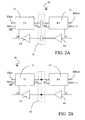
- a chip-to-chip communication system providing precharge and evaluation blocks within a transmitter TX and a receiver RX of the system, such transmitter and receiver having clock signals derived from a common clock signal is also described in the EP Patent application No. 05019644.3 filed on September 9, 2005 and published on March 14, 2007 under No. 1 762 943 in the name of the same applicant and schematically shown in Figures 2A and 2B .
- the system 10 comprises the transmitter TX 11 and the receiver RX 12, connected to each other through a connection block 15.
- the connection block 15 is an inter-chip communication channel.
- the transmitter TX 11 has an output terminal TXout connected to an input terminal RXin of the receiver RX 12 through the connection block 15.
- connection block 15 could be a capacitive connection block, as shown in Figure 2A or an ohmic connection block, as shown in Figure 2B .
- the transmitter TX 11 also has an input terminal TXin receiving an input or data signal D.
- the receiver RX 12 also has an output terminal RXout issuing an output signal Q.
- the input data signal D and the output signal Q are n-bit digital signals.
- the receiver RX 12 is connected to a first terminal G, the reference G being indifferently used to indicate the terminal or the signal applied thereto, for sake of simplicity of description.
- G is the primary clock signal/ terminal.
- the transmitter TX 11 is connected to a second terminal CP as well as to a third terminal SD, also in this case the references CP and SD being indifferently used to indicate the terminals or the signals applied thereto, for sake of simplicity of description.
- CP is the secondary clock signal/terminal
- SD is the preset signal/terminal.
- the first and second control terminals, G and CP, are connected to each other at the connection block 15 through a first 13 and a second buffer 14.
- the transmitter TX 11 is associated with a first chip, conventionally indicated as chip A, referring back to Figure 1
- the receiver RX 12 is associated with a second chip, conventionally indicated as chip B, the first and second chips, A and B, being assembled in a stacked or 3D configuration.
- the primary clock signal G and the secondary clock signal CP are balanced clock trees used to synchronise a bus of the input data signal D.
- the primary clock signal G and the secondary clock signal CP are obtained by a same clock signal.
- the secondary clock signal CP is the transmitter clock signal which is delayed with respect to the primary clock signal G, which is in turn the receiver clock signal.
- the secondary clock signal CP guarantees a correct functional synchronization between the transmitter TX 11 and the receiver RX 12, i.e. between the chips A and B.
- the clock signal is transmitted in the opposite direction of the input data signal D, i.e. from the data receiver chip B to the data transmitter chip A.
- the input data signal D flows from the first chip A to the second chip B, while the clock signals CP and G flow from the second chip B to the first chip A.
- the input data signal D and the clock signals CP and G flow in opposite directions.
- this known system uses of a dedicated clock channel apt to make the two chips isochronal and in phase to each other in order to ensure a correct working.
- the technical problem underlying the present invention is that of providing a synchronizer for a chip-to-chip or 3D communication system having structural and functional characteristics which allows to eliminate the need of a common clock signal transmission or the use of a dedicated clock channel, without requiring the use of synchronizers inside the system itself, thus overcoming the limits which still affect the devices realised according to the prior art and allowing in this way the use of distinct and not related (and thus not iso-frequency) clock domains between 3D stacked chips.
- the solution idea underlying the present invention is that of realising a communication system for the connection between timing non-correlated or also independently clocked synchronous devices, in particular chip-to-chip or 3D, comprising a transmitter and a receiver connected through a channel of the capacitive or resistive type, the receiver being of the self-synchronised type and having at least one asynchronous input stage combined with a synchronous output stage so as to allow the reception of a datum transmitted at any time and to ensure its transmission in a synchronised way with respect to a clock signal.
- a communication system for the connection between timing non correlated synchronous devices of the type comprising at least one transmitter and one receiver inserted between a first and a second voltage reference and connected to each other by means of a transmitting channel in correspondence with respective transmitting and receiving terminals characterised in that said receiver comprises at least one synchronous input stage suitable for receiving on said receiving terminal a datum and associated with a synchronous output stage suitable for transmitting said datum in a synchronised way with a clock signal on a synchronised receiving terminal.
- said receiver could further comprise a feedback block connected between said synchronised receiving terminal and a feedback node, in turn connected to said asynchronous input stage.
- said asynchronous input stage of said receiver could comprise a first and a second high impedance and feedback stage having respective control terminals connected to said feedback node, said first high impedance and feedback stage being inserted between said first voltage reference and said receiving terminal, while said second high impedance and feedback stage is inserted between said receiving terminal and said second voltage reference, said high impedance and feedback stages being suitable for holding a correct voltage value at said receiving terminal supplying it with suitable under-threshold currents.
- said synchronous output stage of said receiver could comprise at least one first and one second latch having respective first input terminals connected to said receiving terminals, second input terminals receiving a negated value of a clock signal and said clock signal, respectively, and output terminals connected to each other and to said synchronised receiving terminal, so that when a latch is under evaluation, the other is disabled, avoiding any electric conflict on said synchronised receiving terminal where said datum being synchronised with said clock signal is present.
- said first and second latches could be of the almost-tspc type.
- said first and second high impedance and feedback stage could be symmetrical to each other and respectively comprise a first and a second transistor, inserted, in series with each other, between said first and second voltage references and said receiving terminal.
- said second transistors of said first and second high impedance and feedback stages could be directly connected to said receiving terminal and have control and bulk terminals connected to said first and second voltage references, respectively, always resulting reverse biased and allowing to store said datum at said receiving terminal under high impedance conditions, thanks to the leakage currents passing through them.
- said first transistors of said first and second high impedance and feedback stages could have respective control terminals realising said first and second control terminal connected to said feedback node.
- said second transistors of said first and second high impedance and feedback stage could be MOS transistors having high leakage currents and said first transistors of said first and second high impedance and feedback stages could be MOS transistors having low leakage currents.
- said first and second latches of said synchronous output stage of said receiver could respectively comprise:
- said feedback block could be formed by a CMOS logic inverter realised by a pair of transistors inserted, in series with each other, between said first and second voltage references, interconnected in correspondence with said feedback node and having respective control terminals connected to each other and to said synchronised receiving terminal.
- the communication system could further comprise an enable block, inserted between said receiving terminal and said second voltage reference and receiving a reset signal.
- said enable block could comprise at least one enable transistor having a control terminal receiving said reset signal.
- said transmitter could be a charge pump transmitter suitable for compensating signal degradations caused by capacitive partitions which characterise the communication system.
- said charge pump transmitter could comprise at least one charge pump capacitor suitable for injecting additional charge into said transmitting terminal.
- said charge pump transmitter could comprise at least one driving section and one switching section interconnected by means of said charge pump capacitor.
- said driving section of said charge pump transmitter could comprise a NAND gate having respective input terminals connected to a first and a second input terminal receiving said datum and said clock signal, respectively, as well as an output terminal connected to a first output terminal, suitable for supplying a first driving signal to said switching section, as well as a logic inverter having an input terminal connected to a third input terminal and receiving said datum and an output terminal connected to a second output terminal, suitable for supplying a second driving signal to the switching section.
- said switching section of said charge pump transmitter could comprise at least a first and a second switch, inserted, in series with each other, between said first and second voltage references, interconnected in correspondence with said transmitting terminal and having respective control terminals connected to said first and second output terminals of said driving section and receiving therefrom said first and second driving signals.
- the communication system could realise a connection of the bidirectional type and in that it comprises at least one pair of reception and transmission blocks, each block comprising at least:
- said transmitter could be a tri-state buffer driven by said additional driving signal so as to ensure a high impedance condition on said output terminal connected to said capacitive channel when in reception mode.
- said pass-gate transistor could have a control terminal receiving said additional driving signal so as to disconnect said receiver under transmission conditions.
- the communication system could further comprise a reset block receiving said additional driving signal and said clock signal and suitable for supplying a reset signal to said receiver.
- the problem is also solved by a method for transmitting a datum from a transmitter to a receiver interconnected by means of a capacitive channel in a communication system for the connection between timing non correlated synchronous devices, the method comprising the steps of:
- said high impedance biasing step of said receiving terminal includes:
- said synchronisation step of said datum could comprise a storage step of said datum in suitable latches, configured in an analogous way and connected to a negated value of said clock signal and to said clock signal, respectively, said latches being inserted between said receiving terminal and said synchronised receiving terminal of said receiver.
- a device for communicating via a transmitting channel with another device that is not timing correlated with the device comprising:
- a communication system 20 includes a capacitive communication channel 25 for the connection between devices 30, 40, in particular chips.
- the channel 25 connects a transmitter 30 and a receiver 40, for which Figure 3 only shows the transmitting TX and receiving RX terminals and the equivalent capacitances C TX and C RX , respectively, connected between these terminals and the ground GND.
- the receiver 40 as used is of the self-synchronised type.
- the receiver 40 comprises an asynchronous input stage associated with a synchronous output stage so as to allow the reception of a datum D transmitted by the transmitter at any time and also ensuring a transmission thereof which is synchronised with the clock signal CP of the receiver itself.
- the word self-synchronised means that, advantageously according to the invention, no clock signal is to be shared by transmitters and receivers of an inter-chip communication system and that it is not necessary to provide a synchroniser to be inserted in these transmitters and receivers to manage the correct overlapping of the clock phases of the interconnected chips.
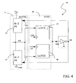
- a receiver realised according to the invention is schematically shown in Figure 4 , globally indicated with 40.
- the receiver 40 comprises an asynchronous input stage 41 inserted between a supply voltage reference Vcc and the ground GND and connected to an input terminal or receiving terminal RX, as well as a synchronous output stage 42, in turn inserted between the receiving terminal RX and a synchronised receiving terminal RXs. Finally, the receiver 40 comprises a feedback block 43 connected between the synchronised receiving terminal RXs and a feedback node FB, in turn connected to the asynchronous input stage 41. It is also to be noted that the feedback block 43 also comprises a part of the asynchronous section of the receiver 40.
- the asynchronous input stage 41 comprises a first 44 and a second high impedance and feedback stage 45, symmetrical to each other and having respective control terminals, Tc1 and Tc2, connected to the feedback node FB.
- the first high impedance and feedback stage 44 is inserted between the supply voltage reference Vcc and the receiving terminal RX, while the second high impedance and feedback stage 45 is inserted between the receiving terminal RX and the ground GND.
- the synchronous output stage 42 comprises a first 47 and a second latch 48 having respective first input terminals connected to the receiving terminals RX, second input terminals receiving a negated value CPN of the clock signal and the clock signal CP, respectively, and output terminals connected to each other and to the synchronised receiving terminal RXs.
- the first and second high impedance stages, 44 and 45 hold a correct voltage value at the input node they are connected to, i.e. at the receiving terminal RX.
- these stages supply this node with suitable under-threshold currents.
- the synchronous output stage 42 is more exactly a synchronising stage comprising the two latches 47 and 48, in particular of the almost-tspc (acronym of the English: "true single phase clock") type.
- the synchronisation stage is called self synchronising according to the possibility of reading the datum at the receiving terminal RX independently from the time relation between the clock signal of the transmitter and that of the receiver.
- the latches 47 and 48 are clocked by the system clock signal CP and by its negated value CPN.
- the other is disabled (with output in high impedance), avoiding any electric conflict on the output node they are connected to, i.e. the synchronised receiving terminal RXs.
- the logic value at the synchronised receiving terminal RXs reflects the value received on the receiving terminal RX, under both rising and falling edge conditions of the clock signal CP itself, the sampling time between the receiving terminal RX and the synchronised receiving terminal RXs being at the best equal to half of the clock period.
- the high impedance condition for the receiving terminal RX is thus always ensured thanks to the high impedance stages, 44 and 45, of the asynchronous input stage 41 connected to this receiving terminal RX, thus allowing to receive a datum D at any time, without problems of synchronisation with the transmitter 30.
- the datum outputting from the receiver 40 onto the synchronised receiving terminal RXs is synchronised with the clock signal CP thanks to the synchronous output stage 42.
- a preferred embodiment of the receiver 40 according to the invention is schematically shown in Figure 5 .
- the receiver 40 comprises the first 44 and the second feedback stage 45, symmetrical to each other and having respective control terminals, Tc1 and Tc2, connected to the feedback node FB.
- the first feedback stage 44 comprises a first and a second transistor, M1 and M2, inserted, in series with each other, between the supply voltage reference and the receiving terminal RX.
- the first transistor M 1 is a P channel MOS transistor having a control or gate terminal realising the first control terminal Tc1 and a bulk terminal connected to the supply voltage reference Vcc while the second transistor M2 is a P channel MOS transistor having a control or gate terminal and a bulk terminal connected to the supply voltage reference Vcc and a drain terminal connected to the receiving terminal RX.
- the second feedback stage 45 comprises a third and a fourth transistor, M3 and M4, inserted, in series with each other, between the receiving terminal RX and the ground GND.
- the third transistor M1 is an N channel MOS transistor having a control or gate terminal and a bulk terminal connected to the ground GND and a drain terminal connected to the receiving terminal RX while the fourth transistor M4 is an N channel MOS transistor having a control or gate terminal realising the second control terminal Tc2 and a bulk terminal connected to the ground GND.
- the second and third transistors, M2 and M3, having the drain terminals connected to the receiving terminal RX, are always reverse biased or locked and allow to store the datum present on this receiving terminal RX under high impedance conditions, thanks to the leakage currents flowing through them, which depend also on the state of the transistors M 1 and M4.
- first and second feedback stages, 44 and 45 implies the use of both MOS transistors having high leakage currents (in particular the transistors M2 and M3) and MOS transistors having low leakage currents (in particular, the transistors M1 and M4).
- the fourth transistor M4 will be reverse biased: the interconnection node pullupZ of the first and of the second transistor, M 1 and M2, is at the supply voltage value Vcc and the current supplied by the first feedback stage 44 will be all that which flows through the second transistor M2 (which is a MOS transistor having high leakage currents) while that drawn by the second feedback stage 45 will be characterised by the crossing of the series of the transistors M3 and M4, and thus will be limited by the fourth transistor M4 (which is a MOS transistor having low leakage currents).
- the high impedance condition always ensured for the receiving terminal RX is an important feature of the receiver 40 according to the invention to allow the reception of the datum D at any time, without synchronisation problems with the transmitter 30.
- the receiver 40 also comprises the first and second latches, 47 and 48, suitably synchronised by the clock signal CP and by its negated value CPN.
- the first latch 47 comprises a fifth M5, a sixth M6 and a seventh transistor M7 inserted, in series with each other, between the supply voltage reference Vcc and the ground GND.
- the seventh transistor M7 inserted, in series with each other, between the supply voltage reference Vcc and the ground GND.
- the eighth and tenth transistors, M8 and M10 have control or gate terminals connected to each other and to the first inner circuit node X1, while the ninth transistor M9 has a control or gate terminal receiving the negated value CPN of the clock signal.
- the second latch 48 has the same circuit configuration of the first latch 47 and the transistors therein comprised have been indicated with the same alphanumeric references with respect to the transistors of the first latch 47, followed by an apostrophe.
- the fifth and the sixth transistor, M5' and M6', as well as the ninth transistor M9' receive the clock signal CP on their control or gate terminals.
- the receiver 40 shown in Figure 5 also comprises a feedback block 43 formed by a CMOS logic inverter realised by a P channel MOS transistor, M11, and by an N channel MOS transistor, M12, inserted, in series with each other, between the supply voltage reference Vcc and the ground GND, interconnected in correspondence with the feedback node FB and having respective control or gate terminals connected to each other and to the synchronised receiving terminal RXs.
- the P channel MOS transistor M11 has its bulk terminal connected to the supply voltage reference and the N channel MOS transistor M12 has its bulk terminal connected to the ground GND.
- the receiver 40 shown in Figure 5 comprises an enable block 49, inserted between the receiving terminal RX and the ground GND and realised by an enable transistor M 13, in particular an N channel MOS transistor, having a control or gate terminal connected to an enable terminal CD suitable for supplying it with a reset signal, always indicated for convenience as CD.
- an enable transistor M 13 in particular an N channel MOS transistor, having a control or gate terminal connected to an enable terminal CD suitable for supplying it with a reset signal, always indicated for convenience as CD.
- the receiver 40 according to the invention is enabled thanks to the reset signal CD but does not need a clock signal being synchronised with the transmitted packets or data, as also previously shown.
- the symmetrical structure of the latches 47 and 48, connected in parallel between the receiving terminal RX and the synchronised receiving terminal RXs and synchronised by opposite signals, CP and CPN allow to have a value of a sampled datum available in both the edges of the clock signal CP of the receiver 40. More precisely, the high value (logic 1) is available on both the edges of the clock signal CP, while the low value (logic 0) is available on both the levels.
- This value of sampled datum is then feedback supplied, thanks to the feedback block 43, to the asynchronous input stage 41 and in particular to the first and second feedback stages, 44 and 45.
- the transmitter 30 is a charge pump transmitter suitable for significantly helping the transmission of a signal in the capacitive channel 25.
- the charge pump transmitter 30 takes care of compensating a signal degradation caused by the capacitive partition occurring in correspondence with the receiving terminal RX, in particular by pumping charge in correspondence with the transmitting terminal TX, thus improving the performances of the communication system 20 as a whole.
- the charge pulse is used in the transmission of a logic value '1' (when considering a reset starting step in which the transmitted and received values are held at a logic value '0'), for helping its correct detection, compensating a possible signal degradation caused by the capacitive partition on the receiving terminal RX.
- a fundamental feature of the charge pump transmitter 30 is its capacity of injecting charge or "boosting" the transmitting terminal TX (and, in consequence, the receiving terminal RX) as much as possible, although keeping the performances as for the frequency of a capacitive channel 25.
- a single cycle of the clock signal CP is enough to reach a voltage pulse level for the terminals TX and RX, no additional delay influencing the operation of the transmitter 30.
- a preferred embodiment of the charge pump transmitter 30 according to the invention is schematically shown in Figure 6 .
- the transmitter 30 comprises a driving section 31 and a switching section 32 interconnected by means of a charge pump capacitor Cboost.
- the driving section 31 has a first input terminal A1 receiving a datum D to be transmitted and a second input terminal B1 receiving the clock signal CP, as well as a third input terminal C1, also receiving the datum D to be transmitted.
- the driving section 31 also has a first output terminal Z1 connected to a terminal of the charge pump capacitor Cboost, as well as to a first input terminal A2 of the switching section 32 and supplying it with a first driving signal DR1, as well as a second output terminal Z2 connected to a second input terminal B2 of the switching section 32 and supplying it with a second driving signal DR2.
- the driving section 31 comprises a NAND gate 33 having respective input terminals connected to the first and second input terminals, A1 and B1, as well as an output terminal connected to the first output terminal Z1 of the driving section 31.
- the driving section 31 also comprises a logic inverter 34 having an input terminal connected to the third input terminal C1 and an output terminal connected to the second output terminal Z2 of the driving section 31.
- the first driving signal DR1 is the result of a logic NAND operation between the datum D to be transmitted and the clock signal CP, while the second driving signal DR2 is the result of a logic inversion of the datum D to be transmitted.
- the switching section 32 comprises a first TM1 and a second switch TM2, in particular realised by MOS transistors, inserted in series with each other between the supply voltage reference Vcc and the ground GND and interconnected in correspondence with the output terminal of the transmitter 30, i.e. of the transmitting terminal TX.
- the first and second switches, TM1 and TM2 have respective control terminals connected to the first and to the second output terminal, Z1 and Z2, of the driving section 31, respectively.
- the first switch TM1 is in particular a P channel MOS transistor inserted between the supply voltage reference Vcc and the transmitting terminal TX, having a gate terminal realising the first input terminal A2 of the switching section 32 and connected to the first output terminal Z1 of the driving section 31, as well as a bulk terminal connected to the supply voltage reference Vcc.
- the second switch TM2 is in particular an N channel MOS transistor inserted between the transmitting terminal TX and the ground GND, having a gate terminal realising the second input terminal B2 of the switching section 32 and connected to the second output terminal Z2 of the driving section 31, as well as a bulk terminal connected to the ground GND.
- the transmitter 30 also comprises a charge pump capacitor Cboost inserted between the first output terminal Z1 of the driving section 31 and the transmitting terminal TX.
- the charge pump transmitter 30 thanks to suitable connections between the charge pump capacitor Cboost and the transmitting terminal TX, injects charge or "boosts" the transmitting terminal TX itself, although keeping the performances as for the frequency of a capacitive channel 25, the charge boost occurring in a single cycle of the clock signal CP.
- the input node of the receiver 40 i.e. the receiving terminal RX
- the receiver 40 only requires that the voltage variation on this receiving terminal RX exceeds a voltage value equal to a threshold voltage of an N channel MOS transistor to ensure the correct operation of the receiver 40 and thus of the system as proposed.
- the receiver 40 can be used as an up/down level shifter and at the same time as synchroniser between two different clock domains, the transmission and reception circuits being placed on distinct chips and potentially characterised by non correlated clock domains and supplies.
- the present invention also relates to an inter-chip communication system of the bidirectional type, according to a further embodiment schematically shown in Figure 7 , this bidirectional embodiment being indicated with 20A.
- the system 20A comprises two reception and transmission blocks 50, in particular a right reception and transmission block 50 R and a left reception and transmission block 50 L , interconnected by the capacitive channel represented by the channel capacitor Ccc.
- Corresponding elements in the two reception and transmission blocks have been indicated with the same alphanumeric reference numbers, followed by the subscripts R and L for indicating elements of the right and left blocks respectively and hereafter, for short, a single generic reception and transmission block 50 will be described.
- this reception and transmission block 50 comprises a transmitter 30 inserted between an input terminal IN and a terminal X of interconnection with the channel capacitor Ccc.
- the terminal X is connected to the supply voltage reference Vcc through a decoupling diode Dd.
- the transmitter 30 also has an enable terminal Ta receiving an additional driving signal T / R.
- the transmitter 30 is a tri-state buffer driven by this additional driving signal T/R so as to ensure a high impedance condition on the interconnection terminal X connected to the channel capacitor Ccc when in reception mode.
- the reception and transmission block 50 also comprises a receiver 40 connected to the terminal X of interconnection with the channel capacitor Ccc by means of a pass-gate transistor Mout and having an output terminal OUT whereon the transmitted datum D is presented, as previously seen in a synchronous way with respect to the clock signal CP received by a clock terminal.
- the pass-gate transistor Mout has a control or gate terminal receiving the additional driving signal T/R in such a way as to disconnect the receiver 40 under transmission conditions.
- the reception and transmission block 50 also comprises a reset block 60 receiving the additional driving signal T/R and the clock signal CP and suitable for supplying the receiver 40 with a reset signal CLEAR.
- the charge pump can be suitably substituted by a generic tri-state buffer, thus obtaining for the transmitting terminal TX a high impedance driving when the capacitive channel 25 should be enabled in reception mode and avoiding at the same time the additional capacitive charge of the charge pump capacitor Cboost inside the transmitter 30.
- the additional driving signal T/R serves as enable signal of this tri-state buffer and allows at the same time to control the pass-gate transistor Mout suitable for disconnecting the receiver 40 from the remainder of the system 20.
- This mechanism obviously operates also in a complementary way, so as to ensure a simultaneous enabling of the left transmitter 30 L and the right receiver 40 R and vice versa.
- the present invention also relates to a method for transmitting a datum D from a transmitter 30 to a receiver 40 interconnected by means of a capacitive channel 25, the method comprising the steps of:
- the step of reception of the datum D on the receiving terminal RX comprises a high impedance biasing step of the receiving terminal RX itself and the step of transmission of the datum D on the synchronised receiving terminal RXs comprises a synchronisation step of this datum D with the clock signal CP.
- the high impedance biasing step of the receiving terminal RX of the receiver 40 occurs by connecting this receiving terminal RX to at least one first and one second high impedance stage, 44 and 45, respectively connected to the supply voltage reference Vcc and to the ground GND.
- this biasing step comprises a control step of these high impedance stages, 44 and 45, comprising a feedback phase of a signal at the synchronised receiving terminal RXs to respective control terminals, Tc1 and Tc2, of these high impedance stages, 44 and 45, this feedback being carried out by means of a feedback block 43 realised by a CMOS inverter.
- the synchronisation step of the datum D comprises a storage step of this datum D in suitable latches, 47 and 48, configured in an analogous way and connected to the negated value CPN of the clock signal and to the clock signal CP, respectively, these latches being inserted between the receiving terminal RX and the synchronised receiving terminal RXs of the receiver 40.
- the chip-to-chip or 3D communication system 20 comprising the above described transmitter 30 and receiver 40 and implementing the above described transmission method, solves the problem linked to the synchronous transmission of data, without requiring the transmission of a common clock signal or the use of a dedicated clock channel, as well as the use of inner synchronisers of the system itself, attaining at the same time several advantages.
- the receiver 40 allows the reception of a datum D at any time and ensures its synchronised transmission with the clock signal CP thanks to the use of an asynchronous input stage associated with a synchronous output stage.
- the asynchronous input stage is symmetrically configured and comprises high impedance stages connected to the receiving terminal for always ensuring its high impedance condition and allowing the correct reception and storage of data under all the conditions.
- the synchronous output stage ensures the transmission of the data received in a way which is synchronised with the clock signal, thanks to the use of latches having symmetrical structure, connected in parallel between the receiving terminal RX and the synchronised receiving terminal RXs and synchronised by the clock signal CP and by its negated value CPN, which thus make the data received in both the edges of the clock signal CP available.
- the system 20 comprises a charge pump transmitter suitable for significantly helping the transmission of a signal in the capacitive channel 25, in particular compensating a signal degradation caused by the capacitive partition and thus improving the performances of the communication system 20 as a whole.
- the charge pump transmitter according to the invention has the capacity of injecting charge or "boosting" the transmitting terminal TX (and, in consequence, the receiving terminal RX) as much as possible, while keeping the performances as for the frequency, a single cycle of the clock signal CP being enough to reach a voltage pulse level for the terminals TX and RX and no additional delay influencing its operation.
- the receiver 40 only requires that the voltage variation on the receiving terminal RX exceeds a voltage value equal to a threshold voltage of an N channel MOS transistor, this receiving terminal RX (which constitutes its input node) accessing the gate terminals of two n-MOS transistors only.
Description
- The present invention relates to a communication system between independently clocked devices, in particular chips.
- The invention particularly, but not exclusively, relates to a chip-to-chip communication system for stacked device, i.e. device comprising at least two chips assembled in a three-dimensional (3D) stacking configuration and the following description is made with reference to this field of application for convenience of explanation only.
- As it is well known, the development of stacking technology for heterogeneous device integration has recently increased in importance.
- Stacking of chips, in which two or more integrated circuits or ICs of different types are placed one on the top of the other in a same package, is an alternative to silicon integration and provides improvements at the system design level in terms of size, cost, speed, power consumption and ease of application for a wide variety of products.
- However, a successful implementation of the stacking or 3D technology deals with state-of-the-art of assembly processes such as wafer back-grinding, handling, die attach, wirebond and alignment. So, the choice of a stacking or 3D technology depends largely on the application of the final chip to be obtained.
- It should be also emphasized that a correct and enhanced chip-to-chip communication in a stacked device is a fundamental feature to be guaranteed, in particular in the scenario of the so-called Systems-on-Chip and Systems-in-Package.
- In fact, by stacking integrated circuits or silicon structures within a same package and ensuring a communication between them can enhance the overall performances of a digital system comprising such structures, as described in the article to Kaustav B. et al. entitled: "3-D ICs: A Novel Chip Design for Improving Deep-Submicrometer Interconnect Performance and Systems-on-Chip Integration", Proceedings of the IEEE, 89(5):602-633, May 2001.
- Moreover, the data vertical communication using Ac interconnection of the wireless type has been recently presented as a stacking or 3D technology really promising for wide band and high speed applications, as described in the article to Kanda K. et al. entitled "1.27Gb/s/pin 3mW/pin wireless superconnect wsc interface scheme", ISSCC Dig. Tech. Papers, pp. 186-187, February 2003. Another vertical data communication system using an AC coupled interconnection is described in the article to Mick et al. entitled: "4GBps High Density AC coupled Interconnection, CICC 2002.
- It is also known from the article to R.J. Drost et al. entitled: "Proximity Communication", IEEE J.Solid-State Circuits, 39(9):1529-1535, September 2004, a prototype based on the vertical communication.
- In this field, synchronization is a key issue for modem integrated systems where the distribution of a global clock signal is not possible or not advisable given the complexity of the systems themselves. In particular, the so-called Globally Asynchronous Locally Synchronous (GALS) approach is important for application to 3D communication systems where clock transmission can be a difficult task at extremely high frequencies but where communication occurs through sampled inter-chip packets.
- A chip-to-chip vertical communication system, based on contactless IO schemes exploiting capacitive coupling as an inter-chip channel, is shown for instance in
Figure 1 . In particular, an upper metal layer of the technology process manufacturing the system is used to form a capacitive channel with the interposition of a dielectric, the chip-to-chip communication system being globally indicated at 1 and hereinafter briefly called thesystem 1. - As shown in
Figure 1 , thesystem 1 comprises a plurality ofcommunication units 2, each comprising atransmitter 3 and areceiver 4. - In particular, the
transmitter 3 resides on a first chip A and thereceiver 4 resides on a second chip B, the first and second chips A and B being assembled in a stacked or 3D configuration, the first chip A being on the top of chip B and thetransmitter 3 and thereceiver 4 being positioned on respective facing surfaces of the chips A and B, more particularly thetransmitter 3 on a bottom surface of the chip A and thereceiver 4 on a top surface of the chip B, with reference to an XYZ axis-system as shown inFigure 1 . Obviously, the above configuration (transmitter 3-chip A; receiver 4-chip B) is considered only as an example, a reverse configuration (transmitter 3-chip B; receiver 4-chip A) being also possible, the same consideration applying. - It should be emphasised that this approach benefits from on-chip communication circuits able to guarantee high performances, low power dissipation and reliable flexibility in data exchange.
- The US patent application published under No.
US 2007/0140397 A1 discloses a method to align a receiver clock signal with a transmitter clock signal based upon a received data signal. - A chip-to-chip communication system, providing precharge and evaluation blocks within a transmitter TX and a receiver RX of the system, such transmitter and receiver having clock signals derived from a common clock signal is also described in the
EP Patent application No. 05019644.3 filed on September 9, 2005 1 762 943 Figures 2A and 2B . - The
system 10 comprises thetransmitter TX 11 and thereceiver RX 12, connected to each other through aconnection block 15. Theconnection block 15 is an inter-chip communication channel. - In particular, the
transmitter TX 11 has an output terminal TXout connected to an input terminal RXin of thereceiver RX 12 through theconnection block 15. - The
connection block 15 could be a capacitive connection block, as shown inFigure 2A or an ohmic connection block, as shown inFigure 2B . - The
transmitter TX 11 also has an input terminal TXin receiving an input or data signal D. In a similar manner, thereceiver RX 12 also has an output terminal RXout issuing an output signal Q. In particular, the input data signal D and the output signal Q are n-bit digital signals. - Furthermore, the
receiver RX 12 is connected to a first terminal G, the reference G being indifferently used to indicate the terminal or the signal applied thereto, for sake of simplicity of description. In particular, G is the primary clock signal/ terminal. - Also, the
transmitter TX 11 is connected to a second terminal CP as well as to a third terminal SD, also in this case the references CP and SD being indifferently used to indicate the terminals or the signals applied thereto, for sake of simplicity of description. In particular, CP is the secondary clock signal/terminal and SD is the preset signal/terminal. - The first and second control terminals, G and CP, are connected to each other at the
connection block 15 through a first 13 and asecond buffer 14. - As already indicated, the
transmitter TX 11 is associated with a first chip, conventionally indicated as chip A, referring back toFigure 1 , while thereceiver RX 12 is associated with a second chip, conventionally indicated as chip B, the first and second chips, A and B, being assembled in a stacked or 3D configuration. - The primary clock signal G and the secondary clock signal CP are balanced clock trees used to synchronise a bus of the input data signal D. In particular, the primary clock signal G and the secondary clock signal CP are obtained by a same clock signal. In the example shown in
figures 2A and 2B , the secondary clock signal CP is the transmitter clock signal which is delayed with respect to the primary clock signal G, which is in turn the receiver clock signal. In this way, the secondary clock signal CP guarantees a correct functional synchronization between thetransmitter TX 11 and thereceiver RX 12, i.e. between the chips A and B. In order to achieve that, the clock signal is transmitted in the opposite direction of the input data signal D, i.e. from the data receiver chip B to the data transmitter chip A. - So, the input data signal D flows from the first chip A to the second chip B, while the clock signals CP and G flow from the second chip B to the first chip A. In summary, the input data signal D and the clock signals CP and G flow in opposite directions.
- While advantageous under several aspects, also this known system uses of a dedicated clock channel apt to make the two chips isochronal and in phase to each other in order to ensure a correct working.
- The technical problem underlying the present invention is that of providing a synchronizer for a chip-to-chip or 3D communication system having structural and functional characteristics which allows to eliminate the need of a common clock signal transmission or the use of a dedicated clock channel, without requiring the use of synchronizers inside the system itself, thus overcoming the limits which still affect the devices realised according to the prior art and allowing in this way the use of distinct and not related (and thus not iso-frequency) clock domains between 3D stacked chips.
- The solution idea underlying the present invention is that of realising a communication system for the connection between timing non-correlated or also independently clocked synchronous devices, in particular chip-to-chip or 3D, comprising a transmitter and a receiver connected through a channel of the capacitive or resistive type, the receiver being of the self-synchronised type and having at least one asynchronous input stage combined with a synchronous output stage so as to allow the reception of a datum transmitted at any time and to ensure its transmission in a synchronised way with respect to a clock signal.
- From now on, for convenience of explanation, reference will be made for the description of the invention to a capacitive channel, however similar considerations and results can also be obtained considering a channel of the resistive type.
- On the basis of this solution idea the technical problem is solved by a communication system for the connection between timing non correlated synchronous devices of the type comprising at least one transmitter and one receiver inserted between a first and a second voltage reference and connected to each other by means of a transmitting channel in correspondence with respective transmitting and receiving terminals characterised in that said receiver comprises at least one synchronous input stage suitable for receiving on said receiving terminal a datum and associated with a synchronous output stage suitable for transmitting said datum in a synchronised way with a clock signal on a synchronised receiving terminal.
- Advantageously according to the invention, said receiver could further comprise a feedback block connected between said synchronised receiving terminal and a feedback node, in turn connected to said asynchronous input stage.
- Moreover, said asynchronous input stage of said receiver could comprise a first and a second high impedance and feedback stage having respective control terminals connected to said feedback node, said first high impedance and feedback stage being inserted between said first voltage reference and said receiving terminal, while said second high impedance and feedback stage is inserted between said receiving terminal and said second voltage reference, said high impedance and feedback stages being suitable for holding a correct voltage value at said receiving terminal supplying it with suitable under-threshold currents.
- Advantageously according to the invention, said synchronous output stage of said receiver could comprise at least one first and one second latch having respective first input terminals connected to said receiving terminals, second input terminals receiving a negated value of a clock signal and said clock signal, respectively, and output terminals connected to each other and to said synchronised receiving terminal, so that when a latch is under evaluation, the other is disabled, avoiding any electric conflict on said synchronised receiving terminal where said datum being synchronised with said clock signal is present.
- Suitably, said first and second latches could be of the almost-tspc type.
- Moreover, said first and second high impedance and feedback stage could be symmetrical to each other and respectively comprise a first and a second transistor, inserted, in series with each other, between said first and second voltage references and said receiving terminal.
- Suitably, said second transistors of said first and second high impedance and feedback stages could be directly connected to said receiving terminal and have control and bulk terminals connected to said first and second voltage references, respectively, always resulting reverse biased and allowing to store said datum at said receiving terminal under high impedance conditions, thanks to the leakage currents passing through them.
- Moreover, said first transistors of said first and second high impedance and feedback stages could have respective control terminals realising said first and second control terminal connected to said feedback node.
- In particular, said second transistors of said first and second high impedance and feedback stage could be MOS transistors having high leakage currents and said first transistors of said first and second high impedance and feedback stages could be MOS transistors having low leakage currents.
- Suitably, said first and second latches of said synchronous output stage of said receiver could respectively comprise:
- first, second and third transistors inserted, in series with each other, between said first and second voltage references, said first and second transistors being interconnected in correspondence with a inner circuit node and having respective control terminals connected to each other and receiving said negated value of said clock signal and said clock signal, respectively, said third transistor having a control terminal connected to said receiving terminal; as well as
- fourth, fifth and sixth transistors inserted, in series with each other, between said first and second voltage references, said fourth and fifth transistors being interconnected in correspondence with said synchronised receiving terminal and said fourth and sixth transistors having respective control terminals connected to each other and to said inner circuit node, said fifth transistor having a control terminal receiving said negated value of said clock signal and said clock signal, respectively.
- Moreover, said feedback block could be formed by a CMOS logic inverter realised by a pair of transistors inserted, in series with each other, between said first and second voltage references, interconnected in correspondence with said feedback node and having respective control terminals connected to each other and to said synchronised receiving terminal.
- Furthermore, advantageously according to the invention, the communication system could further comprise an enable block, inserted between said receiving terminal and said second voltage reference and receiving a reset signal.
- Suitably, said enable block could comprise at least one enable transistor having a control terminal receiving said reset signal.
- Moreover, said transmitter could be a charge pump transmitter suitable for compensating signal degradations caused by capacitive partitions which characterise the communication system.
- In particular, said charge pump transmitter could comprise at least one charge pump capacitor suitable for injecting additional charge into said transmitting terminal.
- Moreover, said charge pump transmitter could comprise at least one driving section and one switching section interconnected by means of said charge pump capacitor.
- In particular, said driving section of said charge pump transmitter could comprise a NAND gate having respective input terminals connected to a first and a second input terminal receiving said datum and said clock signal, respectively, as well as an output terminal connected to a first output terminal, suitable for supplying a first driving signal to said switching section, as well as a logic inverter having an input terminal connected to a third input terminal and receiving said datum and an output terminal connected to a second output terminal, suitable for supplying a second driving signal to the switching section.
- Moreover, said switching section of said charge pump transmitter could comprise at least a first and a second switch, inserted, in series with each other, between said first and second voltage references, interconnected in correspondence with said transmitting terminal and having respective control terminals connected to said first and second output terminals of said driving section and receiving therefrom said first and second driving signals.
- Advantageously according to the invention, the communication system could realise a connection of the bidirectional type and in that it comprises at least one pair of reception and transmission blocks, each block comprising at least:
- one transmitter inserted between an input terminal and an interconnection terminal with the capacitive channel and having an enable terminal receiving an additional driving signal; and
- a receiver connected to said interconnection terminal through a pass-gate transistor and having an output terminal whereon said datum, being transmitted in a synchronised way with respect to said clock signal received by a clock terminal, is present.
- Suitably, said transmitter could be a tri-state buffer driven by said additional driving signal so as to ensure a high impedance condition on said output terminal connected to said capacitive channel when in reception mode.
- Moreover, said pass-gate transistor could have a control terminal receiving said additional driving signal so as to disconnect said receiver under transmission conditions.
- Also, the communication system could further comprise a reset block receiving said additional driving signal and said clock signal and suitable for supplying a reset signal to said receiver.
- The problem is also solved by a method for transmitting a datum from a transmitter to a receiver interconnected by means of a capacitive channel in a communication system for the connection between timing non correlated synchronous devices, the method comprising the steps of:
- reception of a datum in the form of a voltage signal;
- transmission of said datum by said transmitter on a transmitting terminal thereof;
- reception of said datum through said capacitive channel on a receiving terminal of said receiver, including receiving said datum while high impedance biasing said receiving terminal;
- production of a synchronized datum by synchronizing said received datum with a clock signal; and
- transmission of said datum on a synchronised receiving terminal of said receiver
- Moreover, said high impedance biasing step of said receiving terminal includes:
- enabling a first high impedance stage, coupled to a first voltage reference using a feedback signal fed back from said synchronised receiving terminal; and
- disabling a second high impedance stage, coupled to a second voltage reference, using said feedback signal.
- Also, said synchronisation step of said datum could comprise a storage step of said datum in suitable latches, configured in an analogous way and connected to a negated value of said clock signal and to said clock signal, respectively, said latches being inserted between said receiving terminal and said synchronised receiving terminal of said receiver.
- Finally, the problem is solved by a device for communicating via a transmitting channel with another device that is not timing correlated with the device, comprising:
- a receiver that includes:
- a receiving terminal;
- an asynchronous input stage structured to receive on said receiving terminal a datum; and
- a synchronous output stage suitable for outputting said datum, synchronized with a clock signal, on a synchronized receiving terminal.
- The characteristics and advantages of the communication system and method according to the invention will be apparent from the following description of an embodiment thereof given by way of indicative and non limiting example with reference to the annexed drawings.
- In these drawings:
-
Figure 1 shows a general scheme of a chip-to-chip communication system; -
Figures 2A and 2B schematically show a chip-to-chip communication system realised according to the prior art; -
Figure 3 schematically shows a general scheme of a communication channel pattern of the capacitive type; -
Figure 4 schematically shows an asynchronous receiver realised according to the present invention; -
Figure 5 schematically shows a circuit scheme of an embodiment of the self-synchronised receiver realised according to the present invention; -
Figure 6 schematically shows a circuit scheme of an embodiment of the charge pump based transmitter realised according to the present invention; and -
Figure 7 schematically shows a further bidirectional embodiment of the communication system realised according to the present invention. - With reference to these figures, and in particular to
Figure 3 , acommunication system 20 includes acapacitive communication channel 25 for the connection betweendevices - In particular, the
channel 25 connects atransmitter 30 and areceiver 40, for whichFigure 3 only shows the transmitting TX and receiving RX terminals and the equivalent capacitances CTX and CRX, respectively, connected between these terminals and the ground GND. - Advantageously according to the invention, the
receiver 40 as used is of the self-synchronised type. - In particular, the
receiver 40 comprises an asynchronous input stage associated with a synchronous output stage so as to allow the reception of a datum D transmitted by the transmitter at any time and also ensuring a transmission thereof which is synchronised with the clock signal CP of the receiver itself. - In this context, as it will be apparent hereafter in the description, the word self-synchronised means that, advantageously according to the invention, no clock signal is to be shared by transmitters and receivers of an inter-chip communication system and that it is not necessary to provide a synchroniser to be inserted in these transmitters and receivers to manage the correct overlapping of the clock phases of the interconnected chips.
- A receiver realised according to the invention is schematically shown in
Figure 4 , globally indicated with 40. - The
receiver 40 comprises anasynchronous input stage 41 inserted between a supply voltage reference Vcc and the ground GND and connected to an input terminal or receiving terminal RX, as well as asynchronous output stage 42, in turn inserted between the receiving terminal RX and a synchronised receiving terminal RXs. Finally, thereceiver 40 comprises afeedback block 43 connected between the synchronised receiving terminal RXs and a feedback node FB, in turn connected to theasynchronous input stage 41. It is also to be noted that thefeedback block 43 also comprises a part of the asynchronous section of thereceiver 40. - More in detail, the
asynchronous input stage 41 comprises a first 44 and a second high impedance andfeedback stage 45, symmetrical to each other and having respective control terminals, Tc1 and Tc2, connected to the feedback node FB. In particular, the first high impedance andfeedback stage 44 is inserted between the supply voltage reference Vcc and the receiving terminal RX, while the second high impedance andfeedback stage 45 is inserted between the receiving terminal RX and the ground GND. - Further, the
synchronous output stage 42 comprises a first 47 and asecond latch 48 having respective first input terminals connected to the receiving terminals RX, second input terminals receiving a negated value CPN of the clock signal and the clock signal CP, respectively, and output terminals connected to each other and to the synchronised receiving terminal RXs. - The first and second high impedance stages, 44 and 45, hold a correct voltage value at the input node they are connected to, i.e. at the receiving terminal RX. In particular, these stages supply this node with suitable under-threshold currents.
- The
synchronous output stage 42 is more exactly a synchronising stage comprising the twolatches - The synchronisation stage is called self synchronising according to the possibility of reading the datum at the receiving terminal RX independently from the time relation between the clock signal of the transmitter and that of the receiver.
- Suitably the
latches - The high impedance condition for the receiving terminal RX is thus always ensured thanks to the high impedance stages, 44 and 45, of the
asynchronous input stage 41 connected to this receiving terminal RX, thus allowing to receive a datum D at any time, without problems of synchronisation with thetransmitter 30. The datum outputting from thereceiver 40 onto the synchronised receiving terminal RXs is synchronised with the clock signal CP thanks to thesynchronous output stage 42. - A preferred embodiment of the
receiver 40 according to the invention is schematically shown inFigure 5 . - As seen, the
receiver 40 comprises the first 44 and thesecond feedback stage 45, symmetrical to each other and having respective control terminals, Tc1 and Tc2, connected to the feedback node FB. In particular, in the embodiment shown inFigure 5 , thefirst feedback stage 44 comprises a first and a second transistor, M1 and M2, inserted, in series with each other, between the supply voltage reference and the receiving terminal RX. - More in particular, the
first transistor M 1 is a P channel MOS transistor having a control or gate terminal realising the first control terminal Tc1 and a bulk terminal connected to the supply voltage reference Vcc while the second transistor M2 is a P channel MOS transistor having a control or gate terminal and a bulk terminal connected to the supply voltage reference Vcc and a drain terminal connected to the receiving terminal RX. - In a fully symmetrical way, the
second feedback stage 45 comprises a third and a fourth transistor, M3 and M4, inserted, in series with each other, between the receiving terminal RX and the ground GND. - More in particular, the third transistor M1 is an N channel MOS transistor having a control or gate terminal and a bulk terminal connected to the ground GND and a drain terminal connected to the receiving terminal RX while the fourth transistor M4 is an N channel MOS transistor having a control or gate terminal realising the second control terminal Tc2 and a bulk terminal connected to the ground GND.
- It is to be noted that the second and third transistors, M2 and M3, having the drain terminals connected to the receiving terminal RX, are always reverse biased or locked and allow to store the datum present on this receiving terminal RX under high impedance conditions, thanks to the leakage currents flowing through them, which depend also on the state of the
transistors M 1 and M4. - In particular the realisation of these first and second feedback stages, 44 and 45, implies the use of both MOS transistors having high leakage currents (in particular the transistors M2 and M3) and MOS transistors having low leakage currents (in particular, the transistors M1 and M4). In this way if the first transistor M1 is active, then the fourth transistor M4 will be reverse biased: the interconnection node pullupZ of the first and of the second transistor,
M 1 and M2, is at the supply voltage value Vcc and the current supplied by thefirst feedback stage 44 will be all that which flows through the second transistor M2 (which is a MOS transistor having high leakage currents) while that drawn by thesecond feedback stage 45 will be characterised by the crossing of the series of the transistors M3 and M4, and thus will be limited by the fourth transistor M4 (which is a MOS transistor having low leakage currents). - In this way a high logic voltage value previously received is held on the receiving terminal RX.
- Naturally, as it will be obvious for the technician of the field, the dual reasoning is also valid, necessary to hold a low logic value on this receiving terminal RX.
- It is again underlined that the high impedance condition always ensured for the receiving terminal RX is an important feature of the
receiver 40 according to the invention to allow the reception of the datum D at any time, without synchronisation problems with thetransmitter 30. - Suitably, the
receiver 40 also comprises the first and second latches, 47 and 48, suitably synchronised by the clock signal CP and by its negated value CPN. - In particular, the
first latch 47 comprises a fifth M5, a sixth M6 and a seventh transistor M7 inserted, in series with each other, between the supply voltage reference Vcc and the ground GND. In particular; - the fifth transistor M5 is a P channel MOS transistor inserted between the supply voltage reference Vcc and a first inner circuit node X1 and having a bulk terminal connected to the supply voltage reference Vcc;
- the sixth transistor M6 is an N channel MOS transistor inserted between the first inner circuit node X1 and the seventh transistor M7 and having a bulk terminal connected to the ground GND; and
- the seventh transistor M7 is an N channel MOS transistor inserted between the sixth transistor M6 and the ground GND and having a bulk terminal connected to the ground GND.
Suitably, the fifth and sixth transistors, M5 and M6, have control or gate terminals connected to each other and receiving the negated value CPN of the clock signal, while the seventh transistor M7 has a control or gate terminal connected to the receiving terminal RX.
Thefirst latch 47 also comprises an eighth M8, a ninth M9 and a tenth transistor M10 inserted, in series with each other, between the supply voltage reference Vcc and the ground GND and connected between the first inner circuit node X1 and the synchronised receiving terminal RXs. In particular; - the eighth transistor M8 is a P channel MOS transistor inserted between the supply voltage reference Vcc and the synchronised receiving terminal RXs and having a bulk terminal connected to the supply voltage reference Vcc;
- the ninth transistor M9 is an N channel MOS transistor inserted between the synchronised receiving terminal RXs and the seventh transistor M7 and having a bulk terminal connected to the ground GND; and
- the tenth transistor M10 is an N channel MOS transistor inserted between the ninth transistor M9 and the ground GND and having a bulk terminal connected to the ground GND.
- Suitably, the eighth and tenth transistors, M8 and M10, have control or gate terminals connected to each other and to the first inner circuit node X1, while the ninth transistor M9 has a control or gate terminal receiving the negated value CPN of the clock signal.
- The
second latch 48 has the same circuit configuration of thefirst latch 47 and the transistors therein comprised have been indicated with the same alphanumeric references with respect to the transistors of thefirst latch 47, followed by an apostrophe. - In this case, the fifth and the sixth transistor, M5' and M6', as well as the ninth transistor M9' receive the clock signal CP on their control or gate terminals.
- The
receiver 40 shown inFigure 5 also comprises afeedback block 43 formed by a CMOS logic inverter realised by a P channel MOS transistor, M11, and by an N channel MOS transistor, M12, inserted, in series with each other, between the supply voltage reference Vcc and the ground GND, interconnected in correspondence with the feedback node FB and having respective control or gate terminals connected to each other and to the synchronised receiving terminal RXs. In particular, the P channel MOS transistor M11 has its bulk terminal connected to the supply voltage reference and the N channel MOS transistor M12 has its bulk terminal connected to the ground GND. - Finally, the
receiver 40 shown inFigure 5 comprises an enableblock 49, inserted between the receiving terminal RX and the ground GND and realised by anenable transistor M 13, in particular an N channel MOS transistor, having a control or gate terminal connected to an enable terminal CD suitable for supplying it with a reset signal, always indicated for convenience as CD. - It is important to underline that the
receiver 40 according to the invention is enabled thanks to the reset signal CD but does not need a clock signal being synchronised with the transmitted packets or data, as also previously shown. - Let's now see the operation of the
receiver 40 according to the invention in greater detail. - The symmetrical structure of the
latches receiver 40. More precisely, the high value (logic 1) is available on both the edges of the clock signal CP, while the low value (logic 0) is available on both the levels. - This value of sampled datum is then feedback supplied, thanks to the
feedback block 43, to theasynchronous input stage 41 and in particular to the first and second feedback stages, 44 and 45. - Further advantageously according to a preferred embodiment of the invention, the
transmitter 30 is a charge pump transmitter suitable for significantly helping the transmission of a signal in thecapacitive channel 25. - Substantially, the
charge pump transmitter 30 takes care of compensating a signal degradation caused by the capacitive partition occurring in correspondence with the receiving terminal RX, in particular by pumping charge in correspondence with the transmitting terminal TX, thus improving the performances of thecommunication system 20 as a whole. - The charge pulse is used in the transmission of a logic value '1' (when considering a reset starting step in which the transmitted and received values are held at a logic value '0'), for helping its correct detection, compensating a possible signal degradation caused by the capacitive partition on the receiving terminal RX.
- It then immediately occurs that a fundamental feature of the
charge pump transmitter 30 according to the invention is its capacity of injecting charge or "boosting" the transmitting terminal TX (and, in consequence, the receiving terminal RX) as much as possible, although keeping the performances as for the frequency of acapacitive channel 25. In particular, a single cycle of the clock signal CP is enough to reach a voltage pulse level for the terminals TX and RX, no additional delay influencing the operation of thetransmitter 30. - A preferred embodiment of the
charge pump transmitter 30 according to the invention is schematically shown inFigure 6 . - In particular, the
transmitter 30 comprises a drivingsection 31 and aswitching section 32 interconnected by means of a charge pump capacitor Cboost. - More in detail, the driving
section 31 has a first input terminal A1 receiving a datum D to be transmitted and a second input terminal B1 receiving the clock signal CP, as well as a third input terminal C1, also receiving the datum D to be transmitted. The drivingsection 31 also has a first output terminal Z1 connected to a terminal of the charge pump capacitor Cboost, as well as to a first input terminal A2 of theswitching section 32 and supplying it with a first driving signal DR1, as well as a second output terminal Z2 connected to a second input terminal B2 of theswitching section 32 and supplying it with a second driving signal DR2. - In particular, the driving
section 31 comprises aNAND gate 33 having respective input terminals connected to the first and second input terminals, A1 and B1, as well as an output terminal connected to the first output terminal Z1 of the drivingsection 31. The drivingsection 31 also comprises alogic inverter 34 having an input terminal connected to the third input terminal C1 and an output terminal connected to the second output terminal Z2 of the drivingsection 31. - In this way, the first driving signal DR1 is the result of a logic NAND operation between the datum D to be transmitted and the clock signal CP, while the second driving signal DR2 is the result of a logic inversion of the datum D to be transmitted.
- Furthermore, the switching
section 32 comprises a first TM1 and a second switch TM2, in particular realised by MOS transistors, inserted in series with each other between the supply voltage reference Vcc and the ground GND and interconnected in correspondence with the output terminal of thetransmitter 30, i.e. of the transmitting terminal TX. Suitably, the first and second switches, TM1 and TM2, have respective control terminals connected to the first and to the second output terminal, Z1 and Z2, of the drivingsection 31, respectively. - In the embodiment shown in
Figure 6 , the first switch TM1 is in particular a P channel MOS transistor inserted between the supply voltage reference Vcc and the transmitting terminal TX, having a gate terminal realising the first input terminal A2 of theswitching section 32 and connected to the first output terminal Z1 of the drivingsection 31, as well as a bulk terminal connected to the supply voltage reference Vcc. Moreover, the second switch TM2 is in particular an N channel MOS transistor inserted between the transmitting terminal TX and the ground GND, having a gate terminal realising the second input terminal B2 of theswitching section 32 and connected to the second output terminal Z2 of the drivingsection 31, as well as a bulk terminal connected to the ground GND. - The
transmitter 30 also comprises a charge pump capacitor Cboost inserted between the first output terminal Z1 of the drivingsection 31 and the transmitting terminal TX. - It is then immediate to verify that the
transmitter 30 shown inFigure 6 operates as follows: - when the datum D to be transmitted has a low logic value or '0' (D='0'), the transmitting terminal TX is held at a low logic level (TX='0');
- when the datum D to be transmitted has a high logic value or '1' and a high half-period of the clock signal CP starts (D='1' and CP='1') the first driving signal DR1 moves to a low logic value (DR1='0') and triggers a pre-charge phase of the transmitting terminal TX which then reaches a high logic value (TX='1');
- when a low half-period of the clock signal CP starts, the datum D to be transmitted being always a high logic value (D='1' and CP='0'), the first driving signal DR1 rises to a high logic value (DR1='1'), forcing an additional rising transition for the transmitting terminal TX thanks to the charge pump capacitor Cboost which is connected between the first output terminal Z1 (whereon the first driving signal DR1 is present) and the transmitting terminal TX itself. In this way, the value of the voltage at the transmitting terminal TX rises above the high logic value (TX='1+') and an output overvoltage occurs with respect to the supply voltage value Vcc.
- In this way the
charge pump transmitter 30 according to the invention, thanks to suitable connections between the charge pump capacitor Cboost and the transmitting terminal TX, injects charge or "boosts" the transmitting terminal TX itself, although keeping the performances as for the frequency of acapacitive channel 25, the charge boost occurring in a single cycle of the clock signal CP. - It is also to be noted that the input node of the
receiver 40, i.e. the receiving terminal RX, accesses the gate terminals of two n-MOS transistors only. For this reason, advantageously according to the invention, thereceiver 40 only requires that the voltage variation on this receiving terminal RX exceeds a voltage value equal to a threshold voltage of an N channel MOS transistor to ensure the correct operation of thereceiver 40 and thus of the system as proposed. - Finally, it is immediate to verify that the
receiver 40 can be used as an up/down level shifter and at the same time as synchroniser between two different clock domains, the transmission and reception circuits being placed on distinct chips and potentially characterised by non correlated clock domains and supplies. - The present invention also relates to an inter-chip communication system of the bidirectional type, according to a further embodiment schematically shown in
Figure 7 , this bidirectional embodiment being indicated with 20A. - In this case, the
system 20A comprises two reception and transmission blocks 50, in particular a right reception andtransmission block 50R and a left reception andtransmission block 50L, interconnected by the capacitive channel represented by the channel capacitor Ccc. Corresponding elements in the two reception and transmission blocks have been indicated with the same alphanumeric reference numbers, followed by the subscripts R and L for indicating elements of the right and left blocks respectively and hereafter, for short, a single generic reception andtransmission block 50 will be described. - In particular, this reception and
transmission block 50 comprises atransmitter 30 inserted between an input terminal IN and a terminal X of interconnection with the channel capacitor Ccc. Suitably, the terminal X is connected to the supply voltage reference Vcc through a decoupling diode Dd. - The
transmitter 30 also has an enable terminal Ta receiving an additional driving signal T / R. - Suitably, the
transmitter 30 is a tri-state buffer driven by this additional driving signal T/R so as to ensure a high impedance condition on the interconnection terminal X connected to the channel capacitor Ccc when in reception mode. - The reception and
transmission block 50 also comprises areceiver 40 connected to the terminal X of interconnection with the channel capacitor Ccc by means of a pass-gate transistor Mout and having an output terminal OUT whereon the transmitted datum D is presented, as previously seen in a synchronous way with respect to the clock signal CP received by a clock terminal. - Suitably, the pass-gate transistor Mout has a control or gate terminal receiving the additional driving signal T/R in such a way as to disconnect the
receiver 40 under transmission conditions. - The reception and
transmission block 50 also comprises areset block 60 receiving the additional driving signal T/R and the clock signal CP and suitable for supplying thereceiver 40 with a reset signal CLEAR. - In this bidirectional embodiment of the
system 20A, the charge pump can be suitably substituted by a generic tri-state buffer, thus obtaining for the transmitting terminal TX a high impedance driving when thecapacitive channel 25 should be enabled in reception mode and avoiding at the same time the additional capacitive charge of the charge pump capacitor Cboost inside thetransmitter 30. - The additional driving signal T/R serves as enable signal of this tri-state buffer and allows at the same time to control the pass-gate transistor Mout suitable for disconnecting the
receiver 40 from the remainder of thesystem 20. This mechanism obviously operates also in a complementary way, so as to ensure a simultaneous enabling of theleft transmitter 30L and theright receiver 40R and vice versa. - In its most general form, the present invention also relates to a method for transmitting a datum D from a
transmitter 30 to areceiver 40 interconnected by means of acapacitive channel 25, the method comprising the steps of: - reception of a datum D in the form of a voltage signal;
- transmission of the datum D by the
transmitter 30 on a transmitting terminal TX thereof; - reception of the datum D through the
capacitive channel 25 on a receiving terminal RX of thereceiver 40; and - transmission of the datum D on a synchronised receiving terminal RXs of the
receiver 40. - Advantageously according to the invention, the step of reception of the datum D on the receiving terminal RX comprises a high impedance biasing step of the receiving terminal RX itself and the step of transmission of the datum D on the synchronised receiving terminal RXs comprises a synchronisation step of this datum D with the clock signal CP.
- Suitably, the high impedance biasing step of the receiving terminal RX of the
receiver 40 occurs by connecting this receiving terminal RX to at least one first and one second high impedance stage, 44 and 45, respectively connected to the supply voltage reference Vcc and to the ground GND. - Moreover, this biasing step comprises a control step of these high impedance stages, 44 and 45, comprising a feedback phase of a signal at the synchronised receiving terminal RXs to respective control terminals, Tc1 and Tc2, of these high impedance stages, 44 and 45, this feedback being carried out by means of a
feedback block 43 realised by a CMOS inverter. - Further advantageously according to the invention, the synchronisation step of the datum D comprises a storage step of this datum D in suitable latches, 47 and 48, configured in an analogous way and connected to the negated value CPN of the clock signal and to the clock signal CP, respectively, these latches being inserted between the receiving terminal RX and the synchronised receiving terminal RXs of the
receiver 40. - In conclusion, the chip-to-chip or
3D communication system 20 according to the invention, comprising the above describedtransmitter 30 andreceiver 40 and implementing the above described transmission method, solves the problem linked to the synchronous transmission of data, without requiring the transmission of a common clock signal or the use of a dedicated clock channel, as well as the use of inner synchronisers of the system itself, attaining at the same time several advantages. - In particular, advantageously according to the invention, the
receiver 40 allows the reception of a datum D at any time and ensures its synchronised transmission with the clock signal CP thanks to the use of an asynchronous input stage associated with a synchronous output stage. - Further advantageously, the asynchronous input stage is symmetrically configured and comprises high impedance stages connected to the receiving terminal for always ensuring its high impedance condition and allowing the correct reception and storage of data under all the conditions. Moreover, the synchronous output stage ensures the transmission of the data received in a way which is synchronised with the clock signal, thanks to the use of latches having symmetrical structure, connected in parallel between the receiving terminal RX and the synchronised receiving terminal RXs and synchronised by the clock signal CP and by its negated value CPN, which thus make the data received in both the edges of the clock signal CP available.
- Further advantageously according to a preferred embodiment of the invention, the
system 20 comprises a charge pump transmitter suitable for significantly helping the transmission of a signal in thecapacitive channel 25, in particular compensating a signal degradation caused by the capacitive partition and thus improving the performances of thecommunication system 20 as a whole. - In particular, the charge pump transmitter according to the invention has the capacity of injecting charge or "boosting" the transmitting terminal TX (and, in consequence, the receiving terminal RX) as much as possible, while keeping the performances as for the frequency, a single cycle of the clock signal CP being enough to reach a voltage pulse level for the terminals TX and RX and no additional delay influencing its operation.
- Advantageously according to the invention, the
receiver 40 only requires that the voltage variation on the receiving terminal RX exceeds a voltage value equal to a threshold voltage of an N channel MOS transistor, this receiving terminal RX (which constitutes its input node) accessing the gate terminals of two n-MOS transistors only. - Obviously, a technician of the field, aiming at meeting incidental and specific needs, will bring several modifications to the above described communication system, all within the scope of protection of the invention as defined by the following claims.
Claims (23)
- Communication system for the connection between timing non correlated synchronous devices of the type comprising at least one transmitter (30) and one receiver (40) inserted between a first and a second voltage reference (Vcc, GND) and connected to each other by means of a capacitive channel (25) in correspondence with respective transmitting (TX) and receiving (RX) terminals characterised in that said receiver (40) comprises at least one asynchronous input stage (41) suitable for receiving on said receiving terminal (RX) a datum (D) and associated with a synchronous output stage (42) suitable for transmitting said datum (D) in a synchronised way with a clock signal (CP) on a synchronised receiving terminal (RXs) as well as a feedback block (43) connected between said synchronised receiving terminal (RXs) and a feedback node (FB), in turn connected to said asynchronous input stage (41), which comprises a first and a second high impedance and feedback stage (44, 45) having respective control terminals (Tc1, Tc2) connected to said feedback node (FB), said first high impedance and feedback stage (44) being inserted between said first voltage reference (Vcc) and said receiving terminal (RX), while said second high impedance and feedback stage (45) is inserted between said receiving terminal (RX) and said second voltage reference (GND), said high impedance and feedback stages (44, 45) being suitable for holding a correct voltage value at said receiving terminal (RX) supplying it with suitable under-threshold currents.
- Communication system according to claim 1, characterised in that said synchronous output stage (42) of said receiver (40) comprises at least one first and one second latch (47, 48) having respective first input terminals connected to said receiving terminals (RX), second input terminals receiving a negated value (CPN) of a clock signal and said clock signal (CP), respectively, and output terminals connected to each other and to said synchronised receiving terminal (RXs), so that when a latch is under evaluation, the other is disabled, avoiding any electric conflict on said synchronised receiving terminal (RXs) where said datum (D) being synchronised with said clock signal (CP) is present.
- Communication system according to claim 2, characterised in that said first and second latches (47, 48) are of the almost-tspc type.
- Communication system according to claim 3, characterised in that said first and second high impedance and feedback stage (44, 45) are symmetrical to each other and respectively comprise a first and a second transistor (M1, M2; M4, M3), inserted, in series with each other, between said first and second voltage references (Vcc, GND) and said receiving terminal (RX).
- Communication system according to claim 4, characterised in that said second transistors (M2, M3) of said first and second high impedance and feedback stages (44, 45) are directly connected to said receiving terminal (RX) and have control and bulk terminals connected to said first and second voltage references (Vcc, GND), respectively, always resulting reverse biased and allowing to store said datum (D) at said receiving terminal (RX) under high impedance conditions, thanks to the leakage currents passing through them.
- Communication system according to claim 5, characterised in that said first transistors (M1, M4) of said first and second high impedance and feedback stages (44, 45) have respective control terminals realising said first and second control terminal (Tcl, Tc2) connected to said feedback node (FB).
- Communication system according to claim 5, characterised in that said second transistors (M2, M3) of said first and second high impedance and feedback stage (44, 45) are MOS transistors having high leakage currents and in that said first transistors (M1, M4) of said first and second high impedance and feedback stages (44, 45) are MOS transistors having low leakage currents.
- Communication system according to claim 6, characterised in that said first and second latches (47, 48) of said synchronous output stage (42) of said receiver (40) respectively comprise:- first, second and third transistors (M5, M6, M7; M5', M6', M7') inserted, in series with each other, between said first and second voltage references (Vcc, GND), said first and second transistors (M5, M6; M5', M6') being interconnected in correspondence with a inner circuit node (X1, X1') and having respective control terminals connected to each other and receiving said negated value (CPN) of said clock signal and said clock signal (CP), respectively, said third transistor (M7, M7') having a control terminal connected to said receiving terminal (RX); as well as- fourth, fifth and sixth transistors (M8, M9, M10; M8', M9', M10') inserted, in series with each other, between said first and second voltage references (Vcc, GND), said fourth and fifth transistors (M8, M9; M8', M9') being interconnected in correspondence with said synchronised receiving terminal (RXs) and said fourth and sixth transistors (M8, M10; M8', M10') having respective control terminals connected to each other and to said inner circuit node (X1, X1'), said fifth transistor (M9, M9') having a control terminal receiving said negated value (CPN) of said clock signal and said clock signal (CP), respectively.
- Communication system according to claim 1, characterised in that said feedback block (43) is formed by a CMOS logic inverter realised by a pair of transistors (M11, M 12) inserted, in series with each other, between said first and second voltage references (Vcc, GND), interconnected in correspondence with said feedback node (FB) and having respective control terminals connected to each other and to said synchronised receiving terminal (RXs).
- Communication system according to claim 1, characterised in that it further comprises an enable block (49), inserted between said receiving terminal (RX) and said second voltage reference (GND) and receiving a reset signal (CD).
- Communication system according to claim 10, characterised in that said enable block (49) comprises at least one enable transistor (M 13) having a control terminal receiving said reset signal (CD).
- Communication system according to claim 1, characterised in that said transmitter (30) is a charge pump transmitter suitable for compensating signal degradations caused by capacitive partitions which characterise the communication system.
- Communication system according to claim 12, characterised in that said charge pump transmitter (30) comprises at least one charge pump capacitor (Cboost) suitable for injecting additional charge into said transmitting terminal (TX).
- Communication system according to claim 13, characterised in that said charge pump transmitter (30) comprises at least one driving section (31) and one switching section (32) interconnected by means of said charge pump capacitor (Cboost).
- Communication system according to claim 14, characterised in that said driving section (31) of said charge pump transmitter (30) comprises a NAND gate (33) having respective input terminals connected to a first and a second input terminal (A1, B1) receiving said datum (D) and said clock signal (CP), respectively, as well as an output terminal connected to a first output terminal (Z1), suitable for supplying a first driving signal (DR1) to said switching section (32), as well as a logic inverter (34) having an input terminal connected to a third input terminal (C1) and receiving said datum (D) and an output terminal connected to a second output terminal (Z2), suitable for supplying a second driving signal (DR2) to the switching section (32).
- Communication system according to claim 15, characterised in that said switching section (32) of said charge pump transmitter (30) comprises at least a first and a second switch (TM1, TM2), inserted, in series with each other, between said first and second voltage references (Vcc, GND), interconnected in correspondence with said transmitting terminal (TX) and having respective control terminals connected to said first and second output terminals (Z1, Z2) of said driving section (31) and receiving therefrom said first and second driving signals (DR1, DR2).
- Communication system according to any of the preceding claims, characterised in that it realises a connection of the bidirectional type and in that it comprises at least one pair of reception and transmission blocks (50), each block comprising at least:- one transmitter (30) inserted between an input terminal (IN) and an interconnection terminal (X) with the capacitive channel (25) and having an enable terminal (Ta) receiving an additional driving signal (T/R); and- a receiver (40) connected to said interconnection terminal (X) through a pass-gate transistor (Mout) and having an output terminal (OUT) whereon said datum (D), being transmitted in a synchronised way with respect to said clock signal (CP) received by a clock terminal, is present.
- Communication system according to claim 17, characterised in that said transmitter (30) is a tri-state buffer driven by said additional driving signal (T/ R) so as to ensure a high impedance condition on said output terminal (OUT) connected to said capacitive channel (25) when in reception mode.
- Communication system according to claim 18, characterised in that said pass-gate transistor (Mout) has a control terminal receiving said additional driving signal (T/ R) so as to disconnect said receiver (40) under transmission conditions.
- Communication system according to claim 19, characterised in that it further comprises a reset block (60) receiving said additional driving signal (T/R) and said clock signal (CP) and suitable for supplying a reset signal (RESET) to said receiver (40).
- Method for transmitting a datum (D) from a transmitter (30) to a receiver (40) interconnected by means of a capacitive channel (25) in a communication system for the connection between timing non correlated synchronous devices, the method comprising the steps of:- reception of a datum (D) in the form of a voltage signal;- transmission of said datum (D) by said transmitter (30) on a transmitting terminal (TX) thereof;- reception of said datum (D) through said capacitive channel (25) on a receiving terminal (RX) of said receiver (40), including receiving said datum (D) while high impedance biasing said receiving terminal (RX);- production of a synchronized datum by synchronizing said received datum (D) with a clock signal and- transmission of said datum (D) on a synchronised receiving terminal (RXs) of said receiver (40)characterised in that said reception step of said datum (D) on said receiving terminal (RX) comprises a high impedance biasing step of said receiving terminal (RX) itself and said transmission step of said datum (D) on said synchronised receiving terminal (RXs) comprises a synchronisation step of said datum (D) with a clock signal (CP).
- Transmission method according to claim 21, characterised in that said high impedance biasing step of said receiving terminal (RX) includes:enabling a first high impedance stage (44), coupled to a first voltage reference (Vcc) using a feedback signal fed back from said synchronised receiving terminal (RXs) ; anddisabling a second high impedance stage (45), coupled to a second voltage reference (GND), using said feedback signal.
- Transmission method according to claim 22, characterised in that said synchronisation step of said datum (D) comprises a storage step of said datum (D) in suitable latches (47, 48), configured in an analogous way and connected to a negated value (CPN) of said clock signal and to said clock signal (CP), respectively, said latches being inserted between said receiving terminal (RX) and said synchronised receiving terminal (RXs) of said receiver (40).
Applications Claiming Priority (1)
| Application Number | Priority Date | Filing Date | Title |
|---|---|---|---|
| IT002451A ITMI20072451A1 (en) | 2007-12-31 | 2007-12-31 | COMMUNICATION SYSTEM FOR THE CONNECTION BETWEEN SYNCHRONOUS DEVICES NOT TEMPORALLY RELATED |
Publications (3)
| Publication Number | Publication Date |
|---|---|
| EP2075708A2 EP2075708A2 (en) | 2009-07-01 |
| EP2075708A3 EP2075708A3 (en) | 2010-05-12 |
| EP2075708B1 true EP2075708B1 (en) | 2013-02-13 |
Family
ID=40315677
Family Applications (1)
| Application Number | Title | Priority Date | Filing Date |
|---|---|---|---|
| EP08022446A Active EP2075708B1 (en) | 2007-12-31 | 2008-12-24 | Communication system between independently clocked devices |
Country Status (3)
| Country | Link |
|---|---|
| US (1) | US7772888B2 (en) |
| EP (1) | EP2075708B1 (en) |
| IT (1) | ITMI20072451A1 (en) |
Families Citing this family (7)
| Publication number | Priority date | Publication date | Assignee | Title |
|---|---|---|---|---|
| US8150315B2 (en) | 2010-06-29 | 2012-04-03 | Stmicroelectronics S.R.L. | Method for verifying the alignment between integrated electronic devices |
| US8340576B2 (en) | 2010-06-29 | 2012-12-25 | Stmicroelectronics S.R.L. | Electronic circuit for communicating through capacitive coupling |
| US9147636B2 (en) | 2011-06-29 | 2015-09-29 | Stmicroelectronics S.R.L. | Method for verifying the alignment between integrated electronic devices |
| US8829955B1 (en) * | 2013-03-14 | 2014-09-09 | Analog Devices, Inc. | Isolator-based transmission system with side isolator channel for refresh signals |
| US9348357B2 (en) | 2014-06-30 | 2016-05-24 | International Business Machines Corporation | Stitchable global clock for 3D chips |
| JP2016029785A (en) * | 2014-07-18 | 2016-03-03 | 株式会社東芝 | Communication system |
| CN107078977B (en) | 2014-09-24 | 2020-10-16 | 美国亚德诺半导体公司 | Circuit and system for multipath isolator communication |
Family Cites Families (4)
| Publication number | Priority date | Publication date | Assignee | Title |
|---|---|---|---|---|
| JPS6220362A (en) * | 1985-07-19 | 1987-01-28 | Hitachi Ltd | Signal transmission circuit for laminated electric circuit |
| EP1762943B1 (en) | 2005-09-09 | 2014-07-09 | STMicroelectronics Srl | Chip-to-chip communication system |
| US7664215B2 (en) * | 2005-12-21 | 2010-02-16 | Intel Corporation | Signal alignment based on data signal |
| ITMI20072450A1 (en) * | 2007-12-31 | 2009-07-01 | St Microelectronics Srl | COMMUNICATION SYSTEM BETWEEN A FIRST AND A SECOND SYNCHRONOUS NON-RELATED DEVICE. |
-
2007
- 2007-12-31 IT IT002451A patent/ITMI20072451A1/en unknown
-
2008
- 2008-12-24 EP EP08022446A patent/EP2075708B1/en active Active
- 2008-12-29 US US12/345,479 patent/US7772888B2/en active Active
Also Published As
| Publication number | Publication date |
|---|---|
| EP2075708A3 (en) | 2010-05-12 |
| EP2075708A2 (en) | 2009-07-01 |
| US20090168938A1 (en) | 2009-07-02 |
| ITMI20072451A1 (en) | 2009-07-01 |
| US7772888B2 (en) | 2010-08-10 |
Similar Documents
| Publication | Publication Date | Title |
|---|---|---|
| EP2075708B1 (en) | Communication system between independently clocked devices | |
| EP2075710B1 (en) | Communication system between first and second independently clocked devices | |
| US7808276B2 (en) | Chip-to-chip communication system and method | |
| US7821293B2 (en) | Asynchronous interconnection system for 3D interchip communication | |
| CN102709272B (en) | Fault tolerant unit and method for through silicon via | |
| US7859117B2 (en) | Clocking architecture in stacked and bonded dice | |
| US5555540A (en) | ASIC bus structure | |
| CN112817906B (en) | Clock domain system of interconnected bare cores and management method thereof | |
| CN102623039A (en) | Clock reproducing and timing method in a system having a plurality of devices and memory controller with flexible data alignment | |
| CN104424154B (en) | General serial peripheral interface | |
| US10397142B2 (en) | Multi-chip structure having flexible input/output chips | |
| CN112817908B (en) | High-speed expansion system and expansion method between bare chips | |
| CN101427226A (en) | Serial communications bus with active pullup | |
| CN105487994B (en) | Expansible 2.5D interface architectures | |
| CN106505993B (en) | Semiconductor circuit including flip-flop | |
| US8873668B2 (en) | Communications arrangement for a system in package | |
| US6266265B1 (en) | Memory module using a vacant pin terminal for balancing parasitic capacitive loads | |
| US11575383B2 (en) | Clocking system and a method of clock synchronization | |
| Sim et al. | High-speed links for memory interface | |
| Zhuang et al. | A design approach for gals based systems-on-chip | |
| Belleville et al. | A single TSV-rail 3D quasi delay insensitive asynchronous signaling | |
| Stanford | Low-Cost 3D Chip Stacking with ThruChip Wireless Connections |
Legal Events
| Date | Code | Title | Description |
|---|---|---|---|
| PUAI | Public reference made under article 153(3) epc to a published international application that has entered the european phase |
Free format text: ORIGINAL CODE: 0009012 |
|
| AK | Designated contracting states |
Kind code of ref document: A2 Designated state(s): AT BE BG CH CY CZ DE DK EE ES FI FR GB GR HR HU IE IS IT LI LT LU LV MC MT NL NO PL PT RO SE SI SK TR |
|
| AX | Request for extension of the european patent |
Extension state: AL BA MK RS |
|
| RAP1 | Party data changed (applicant data changed or rights of an application transferred) |
Owner name: STMICROELECTRONICS SRL |
|
| PUAL | Search report despatched |
Free format text: ORIGINAL CODE: 0009013 |
|
| RIC1 | Information provided on ipc code assigned before grant |
Ipc: H04L 7/00 20060101ALI20100326BHEP Ipc: G06F 13/40 20060101AFI20090526BHEP |
|
| AK | Designated contracting states |
Kind code of ref document: A3 Designated state(s): AT BE BG CH CY CZ DE DK EE ES FI FR GB GR HR HU IE IS IT LI LT LU LV MC MT NL NO PL PT RO SE SI SK TR |
|
| AX | Request for extension of the european patent |
Extension state: AL BA MK RS |
|
| 17P | Request for examination filed |
Effective date: 20100922 |
|
| 17Q | First examination report despatched |
Effective date: 20101115 |
|
| AKX | Designation fees paid |
Designated state(s): DE FR GB IT |
|
| RAP1 | Party data changed (applicant data changed or rights of an application transferred) |
Owner name: STMICROELECTRONICS SRL |
|
| GRAP | Despatch of communication of intention to grant a patent |
Free format text: ORIGINAL CODE: EPIDOSNIGR1 |
|
| RIN1 | Information on inventor provided before grant (corrected) |
Inventor name: GUERRIERI, ROBERTO Inventor name: FAZZI, ALBERTO Inventor name: CANEGALLO, ROBERTO Inventor name: CICCARELLI, LUCA Inventor name: MAGAGNI, LUCA |
|
| GRAS | Grant fee paid |
Free format text: ORIGINAL CODE: EPIDOSNIGR3 |
|
| GRAA | (expected) grant |
Free format text: ORIGINAL CODE: 0009210 |
|
| AK | Designated contracting states |
Kind code of ref document: B1 Designated state(s): DE FR GB IT |
|
| REG | Reference to a national code |
Ref country code: GB Ref legal event code: FG4D |
|
| REG | Reference to a national code |
Ref country code: DE Ref legal event code: R096 Ref document number: 602008022051 Country of ref document: DE Effective date: 20130411 |
|
| REG | Reference to a national code |
Ref country code: DE Ref document number: 602008022051 Representative=s name: SCHMITT-NILSON SCHRAUD WAIBEL WOHLFROM PATENTA, DE Ref legal event code: R082 Country of ref document: DE Ref country code: DE Ref legal event code: R082 Ref document number: 602008022051 Country of ref document: DE Representative=s name: , |
|
| PLBE | No opposition filed within time limit |
Free format text: ORIGINAL CODE: 0009261 |
|
| STAA | Information on the status of an ep patent application or granted ep patent |
Free format text: STATUS: NO OPPOSITION FILED WITHIN TIME LIMIT |
|
| PG25 | Lapsed in a contracting state [announced via postgrant information from national office to epo] |
Ref country code: IT Free format text: LAPSE BECAUSE OF FAILURE TO SUBMIT A TRANSLATION OF THE DESCRIPTION OR TO PAY THE FEE WITHIN THE PRESCRIBED TIME-LIMIT Effective date: 20130213 |
|
| 26N | No opposition filed |
Effective date: 20131114 |
|
| REG | Reference to a national code |
Ref country code: DE Ref legal event code: R097 Ref document number: 602008022051 Country of ref document: DE Effective date: 20131114 |
|
| GBPC | Gb: european patent ceased through non-payment of renewal fee |
Effective date: 20131224 |
|
| REG | Reference to a national code |
Ref country code: FR Ref legal event code: ST Effective date: 20140829 |
|
| PG25 | Lapsed in a contracting state [announced via postgrant information from national office to epo] |
Ref country code: FR Free format text: LAPSE BECAUSE OF NON-PAYMENT OF DUE FEES Effective date: 20131231 Ref country code: GB Free format text: LAPSE BECAUSE OF NON-PAYMENT OF DUE FEES Effective date: 20131224 |
|
| REG | Reference to a national code |
Ref country code: DE Ref legal event code: R082 Ref document number: 602008022051 Country of ref document: DE Representative=s name: SCHMITT-NILSON SCHRAUD WAIBEL WOHLFROM PATENTA, DE |
|
| PGFP | Annual fee paid to national office [announced via postgrant information from national office to epo] |
Ref country code: DE Payment date: 20231121 Year of fee payment: 16 |