EP2075603A1 - Optical waveguide for luminescent device and manufacturing method thereof - Google Patents
Optical waveguide for luminescent device and manufacturing method thereof Download PDFInfo
- Publication number
- EP2075603A1 EP2075603A1 EP08022186A EP08022186A EP2075603A1 EP 2075603 A1 EP2075603 A1 EP 2075603A1 EP 08022186 A EP08022186 A EP 08022186A EP 08022186 A EP08022186 A EP 08022186A EP 2075603 A1 EP2075603 A1 EP 2075603A1
- Authority
- EP
- European Patent Office
- Prior art keywords
- core
- cladding layer
- optical waveguide
- luminescent device
- coating material
- Prior art date
- Legal status (The legal status is an assumption and is not a legal conclusion. Google has not performed a legal analysis and makes no representation as to the accuracy of the status listed.)
- Withdrawn
Links
- 230000003287 optical effect Effects 0.000 title claims abstract description 64
- 238000004519 manufacturing process Methods 0.000 title claims abstract description 16
- 239000000463 material Substances 0.000 claims abstract description 110
- 238000005253 cladding Methods 0.000 claims abstract description 105
- 239000011248 coating agent Substances 0.000 claims abstract description 67
- 238000000576 coating method Methods 0.000 claims abstract description 67
- 239000010410 layer Substances 0.000 claims description 134
- 229920005989 resin Polymers 0.000 claims description 63
- 239000011347 resin Substances 0.000 claims description 63
- 239000011247 coating layer Substances 0.000 claims description 36
- 239000002245 particle Substances 0.000 claims description 28
- 238000000149 argon plasma sintering Methods 0.000 claims description 18
- 238000011049 filling Methods 0.000 claims description 11
- 238000004382 potting Methods 0.000 claims description 6
- 239000007769 metal material Substances 0.000 claims description 3
- 239000011800 void material Substances 0.000 claims description 3
- 230000001902 propagating effect Effects 0.000 abstract description 9
- 239000011162 core material Substances 0.000 description 75
- 230000015572 biosynthetic process Effects 0.000 description 37
- 238000000034 method Methods 0.000 description 35
- 238000010438 heat treatment Methods 0.000 description 19
- 238000011161 development Methods 0.000 description 9
- -1 polyethylenes Polymers 0.000 description 8
- 239000000243 solution Substances 0.000 description 7
- 239000002966 varnish Substances 0.000 description 7
- 239000010408 film Substances 0.000 description 6
- 238000004528 spin coating Methods 0.000 description 6
- 229920001187 thermosetting polymer Polymers 0.000 description 5
- YEJRWHAVMIAJKC-UHFFFAOYSA-N 4-Butyrolactone Chemical compound O=C1CCCO1 YEJRWHAVMIAJKC-UHFFFAOYSA-N 0.000 description 4
- VYPSYNLAJGMNEJ-UHFFFAOYSA-N silicon dioxide Inorganic materials O=[Si]=O VYPSYNLAJGMNEJ-UHFFFAOYSA-N 0.000 description 4
- 239000000758 substrate Substances 0.000 description 4
- 239000007864 aqueous solution Substances 0.000 description 3
- 239000003822 epoxy resin Substances 0.000 description 3
- QSHDDOUJBYECFT-UHFFFAOYSA-N mercury Chemical compound [Hg] QSHDDOUJBYECFT-UHFFFAOYSA-N 0.000 description 3
- 239000002184 metal Substances 0.000 description 3
- 238000002156 mixing Methods 0.000 description 3
- 239000000203 mixture Substances 0.000 description 3
- 230000002093 peripheral effect Effects 0.000 description 3
- 229920000647 polyepoxide Polymers 0.000 description 3
- 229920001721 polyimide Polymers 0.000 description 3
- 239000010453 quartz Substances 0.000 description 3
- 239000002904 solvent Substances 0.000 description 3
- VYZAMTAEIAYCRO-UHFFFAOYSA-N Chromium Chemical compound [Cr] VYZAMTAEIAYCRO-UHFFFAOYSA-N 0.000 description 2
- XUIMIQQOPSSXEZ-UHFFFAOYSA-N Silicon Chemical compound [Si] XUIMIQQOPSSXEZ-UHFFFAOYSA-N 0.000 description 2
- GWEVSGVZZGPLCZ-UHFFFAOYSA-N Titan oxide Chemical compound O=[Ti]=O GWEVSGVZZGPLCZ-UHFFFAOYSA-N 0.000 description 2
- MCMNRKCIXSYSNV-UHFFFAOYSA-N Zirconium dioxide Chemical compound O=[Zr]=O MCMNRKCIXSYSNV-UHFFFAOYSA-N 0.000 description 2
- 239000000853 adhesive Substances 0.000 description 2
- 230000001070 adhesive effect Effects 0.000 description 2
- 238000005266 casting Methods 0.000 description 2
- 230000008859 change Effects 0.000 description 2
- 238000007598 dipping method Methods 0.000 description 2
- 229920006351 engineering plastic Polymers 0.000 description 2
- LZCLXQDLBQLTDK-UHFFFAOYSA-N ethyl 2-hydroxypropanoate Chemical compound CCOC(=O)C(C)O LZCLXQDLBQLTDK-UHFFFAOYSA-N 0.000 description 2
- 238000002347 injection Methods 0.000 description 2
- 239000007924 injection Substances 0.000 description 2
- 238000000465 moulding Methods 0.000 description 2
- 239000003960 organic solvent Substances 0.000 description 2
- 239000009719 polyimide resin Substances 0.000 description 2
- 229920000098 polyolefin Polymers 0.000 description 2
- 230000005855 radiation Effects 0.000 description 2
- 239000010703 silicon Substances 0.000 description 2
- 229910052710 silicon Inorganic materials 0.000 description 2
- 239000000126 substance Substances 0.000 description 2
- 229920005992 thermoplastic resin Polymers 0.000 description 2
- 230000000007 visual effect Effects 0.000 description 2
- OEPOKWHJYJXUGD-UHFFFAOYSA-N 2-(3-phenylmethoxyphenyl)-1,3-thiazole-4-carbaldehyde Chemical compound O=CC1=CSC(C=2C=C(OCC=3C=CC=CC=3)C=CC=2)=N1 OEPOKWHJYJXUGD-UHFFFAOYSA-N 0.000 description 1
- NQXNYVAALXGLQT-UHFFFAOYSA-N 2-[4-[9-[4-(2-hydroxyethoxy)phenyl]fluoren-9-yl]phenoxy]ethanol Chemical compound C1=CC(OCCO)=CC=C1C1(C=2C=CC(OCCO)=CC=2)C2=CC=CC=C2C2=CC=CC=C21 NQXNYVAALXGLQT-UHFFFAOYSA-N 0.000 description 1
- 239000004925 Acrylic resin Substances 0.000 description 1
- 229920000178 Acrylic resin Polymers 0.000 description 1
- 239000004641 Diallyl-phthalate Substances 0.000 description 1
- 229920000877 Melamine resin Polymers 0.000 description 1
- CTQNGGLPUBDAKN-UHFFFAOYSA-N O-Xylene Chemical compound CC1=CC=CC=C1C CTQNGGLPUBDAKN-UHFFFAOYSA-N 0.000 description 1
- 239000004952 Polyamide Substances 0.000 description 1
- 239000004698 Polyethylene Substances 0.000 description 1
- 239000004642 Polyimide Substances 0.000 description 1
- 239000004721 Polyphenylene oxide Substances 0.000 description 1
- 239000004734 Polyphenylene sulfide Substances 0.000 description 1
- 239000004743 Polypropylene Substances 0.000 description 1
- 239000004793 Polystyrene Substances 0.000 description 1
- 239000007983 Tris buffer Substances 0.000 description 1
- 229920001807 Urea-formaldehyde Polymers 0.000 description 1
- BZHJMEDXRYGGRV-UHFFFAOYSA-N Vinyl chloride Chemical compound ClC=C BZHJMEDXRYGGRV-UHFFFAOYSA-N 0.000 description 1
- 229920000122 acrylonitrile butadiene styrene Polymers 0.000 description 1
- 125000002723 alicyclic group Chemical group 0.000 description 1
- 150000004996 alkyl benzenes Chemical class 0.000 description 1
- PNEYBMLMFCGWSK-UHFFFAOYSA-N aluminium oxide Inorganic materials [O-2].[O-2].[O-2].[Al+3].[Al+3] PNEYBMLMFCGWSK-UHFFFAOYSA-N 0.000 description 1
- QUDWYFHPNIMBFC-UHFFFAOYSA-N bis(prop-2-enyl) benzene-1,2-dicarboxylate Chemical compound C=CCOC(=O)C1=CC=CC=C1C(=O)OCC=C QUDWYFHPNIMBFC-UHFFFAOYSA-N 0.000 description 1
- 239000001273 butane Substances 0.000 description 1
- YFNONBGXNFCTMM-UHFFFAOYSA-N butoxybenzene Chemical group CCCCOC1=CC=CC=C1 YFNONBGXNFCTMM-UHFFFAOYSA-N 0.000 description 1
- DXXIFYGOFNDTND-UHFFFAOYSA-N carbonic acid;pentan-3-one Chemical compound OC(O)=O.CCC(=O)CC DXXIFYGOFNDTND-UHFFFAOYSA-N 0.000 description 1
- 229920002678 cellulose Polymers 0.000 description 1
- 239000001913 cellulose Substances 0.000 description 1
- 239000003086 colorant Substances 0.000 description 1
- GYZLOYUZLJXAJU-UHFFFAOYSA-N diglycidyl ether Chemical compound C1OC1COCC1CO1 GYZLOYUZLJXAJU-UHFFFAOYSA-N 0.000 description 1
- 238000001035 drying Methods 0.000 description 1
- 238000010894 electron beam technology Methods 0.000 description 1
- 238000005530 etching Methods 0.000 description 1
- 229940116333 ethyl lactate Drugs 0.000 description 1
- 229920006244 ethylene-ethyl acrylate Polymers 0.000 description 1
- 239000010419 fine particle Substances 0.000 description 1
- 239000011521 glass Substances 0.000 description 1
- LNEPOXFFQSENCJ-UHFFFAOYSA-N haloperidol Chemical compound C1CC(O)(C=2C=CC(Cl)=CC=2)CCN1CCCC(=O)C1=CC=C(F)C=C1 LNEPOXFFQSENCJ-UHFFFAOYSA-N 0.000 description 1
- 125000004435 hydrogen atom Chemical group [H]* 0.000 description 1
- 150000003949 imides Chemical class 0.000 description 1
- 238000007654 immersion Methods 0.000 description 1
- 229920000554 ionomer Polymers 0.000 description 1
- 239000004973 liquid crystal related substance Substances 0.000 description 1
- 238000012986 modification Methods 0.000 description 1
- 230000004048 modification Effects 0.000 description 1
- OFBQJSOFQDEBGM-UHFFFAOYSA-N n-pentane Natural products CCCCC OFBQJSOFQDEBGM-UHFFFAOYSA-N 0.000 description 1
- 229920001568 phenolic resin Polymers 0.000 description 1
- 239000005011 phenolic resin Substances 0.000 description 1
- 229920003023 plastic Polymers 0.000 description 1
- 239000004033 plastic Substances 0.000 description 1
- 229920002492 poly(sulfone) Polymers 0.000 description 1
- 229920002647 polyamide Polymers 0.000 description 1
- 229920001707 polybutylene terephthalate Polymers 0.000 description 1
- 229920000515 polycarbonate Polymers 0.000 description 1
- 239000004417 polycarbonate Substances 0.000 description 1
- 229920000573 polyethylene Polymers 0.000 description 1
- 239000011112 polyethylene naphthalate Substances 0.000 description 1
- 229920000139 polyethylene terephthalate Polymers 0.000 description 1
- 229920000306 polymethylpentene Polymers 0.000 description 1
- 229920006324 polyoxymethylene Polymers 0.000 description 1
- 229920006380 polyphenylene oxide Polymers 0.000 description 1
- 229920000069 polyphenylene sulfide Polymers 0.000 description 1
- 229920001155 polypropylene Polymers 0.000 description 1
- 229920001296 polysiloxane Polymers 0.000 description 1
- 229920002223 polystyrene Polymers 0.000 description 1
- 229920000874 polytetramethylene terephthalate Polymers 0.000 description 1
- 229920002689 polyvinyl acetate Polymers 0.000 description 1
- 229920002451 polyvinyl alcohol Polymers 0.000 description 1
- 235000019422 polyvinyl alcohol Nutrition 0.000 description 1
- 238000007639 printing Methods 0.000 description 1
- 230000008569 process Effects 0.000 description 1
- 238000012545 processing Methods 0.000 description 1
- 238000003672 processing method Methods 0.000 description 1
- KCTAWXVAICEBSD-UHFFFAOYSA-N prop-2-enoyloxy prop-2-eneperoxoate Chemical compound C=CC(=O)OOOC(=O)C=C KCTAWXVAICEBSD-UHFFFAOYSA-N 0.000 description 1
- 230000000644 propagated effect Effects 0.000 description 1
- 230000009467 reduction Effects 0.000 description 1
- 239000011342 resin composition Substances 0.000 description 1
- 230000004044 response Effects 0.000 description 1
- 238000006748 scratching Methods 0.000 description 1
- 230000002393 scratching effect Effects 0.000 description 1
- 239000004065 semiconductor Substances 0.000 description 1
- 229920002050 silicone resin Polymers 0.000 description 1
- 239000007921 spray Substances 0.000 description 1
- 230000002195 synergetic effect Effects 0.000 description 1
- 238000012360 testing method Methods 0.000 description 1
- 239000010409 thin film Substances 0.000 description 1
- 229920006305 unsaturated polyester Polymers 0.000 description 1
- 239000008096 xylene Substances 0.000 description 1
Images


Classifications
-
- H—ELECTRICITY
- H04—ELECTRIC COMMUNICATION TECHNIQUE
- H04M—TELEPHONIC COMMUNICATION
- H04M1/00—Substation equipment, e.g. for use by subscribers
- H04M1/02—Constructional features of telephone sets
- H04M1/22—Illumination; Arrangements for improving the visibility of characters on dials
-
- G—PHYSICS
- G02—OPTICS
- G02B—OPTICAL ELEMENTS, SYSTEMS OR APPARATUS
- G02B6/00—Light guides; Structural details of arrangements comprising light guides and other optical elements, e.g. couplings
- G02B6/10—Light guides; Structural details of arrangements comprising light guides and other optical elements, e.g. couplings of the optical waveguide type
- G02B6/12—Light guides; Structural details of arrangements comprising light guides and other optical elements, e.g. couplings of the optical waveguide type of the integrated circuit kind
- G02B6/122—Basic optical elements, e.g. light-guiding paths
-
- G—PHYSICS
- G02—OPTICS
- G02B—OPTICAL ELEMENTS, SYSTEMS OR APPARATUS
- G02B6/00—Light guides; Structural details of arrangements comprising light guides and other optical elements, e.g. couplings
- G02B6/0001—Light guides; Structural details of arrangements comprising light guides and other optical elements, e.g. couplings specially adapted for lighting devices or systems
-
- G—PHYSICS
- G02—OPTICS
- G02B—OPTICAL ELEMENTS, SYSTEMS OR APPARATUS
- G02B6/00—Light guides; Structural details of arrangements comprising light guides and other optical elements, e.g. couplings
- G02B6/10—Light guides; Structural details of arrangements comprising light guides and other optical elements, e.g. couplings of the optical waveguide type
- G02B6/12—Light guides; Structural details of arrangements comprising light guides and other optical elements, e.g. couplings of the optical waveguide type of the integrated circuit kind
- G02B6/13—Integrated optical circuits characterised by the manufacturing method
-
- G—PHYSICS
- G02—OPTICS
- G02B—OPTICAL ELEMENTS, SYSTEMS OR APPARATUS
- G02B6/00—Light guides; Structural details of arrangements comprising light guides and other optical elements, e.g. couplings
- G02B6/10—Light guides; Structural details of arrangements comprising light guides and other optical elements, e.g. couplings of the optical waveguide type
- G02B6/12—Light guides; Structural details of arrangements comprising light guides and other optical elements, e.g. couplings of the optical waveguide type of the integrated circuit kind
- G02B6/13—Integrated optical circuits characterised by the manufacturing method
- G02B6/138—Integrated optical circuits characterised by the manufacturing method by using polymerisation
-
- H—ELECTRICITY
- H04—ELECTRIC COMMUNICATION TECHNIQUE
- H04M—TELEPHONIC COMMUNICATION
- H04M19/00—Current supply arrangements for telephone systems
- H04M19/02—Current supply arrangements for telephone systems providing ringing current or supervisory tones, e.g. dialling tone or busy tone
- H04M19/04—Current supply arrangements for telephone systems providing ringing current or supervisory tones, e.g. dialling tone or busy tone the ringing-current being generated at the substations
-
- G—PHYSICS
- G02—OPTICS
- G02B—OPTICAL ELEMENTS, SYSTEMS OR APPARATUS
- G02B6/00—Light guides; Structural details of arrangements comprising light guides and other optical elements, e.g. couplings
- G02B6/0001—Light guides; Structural details of arrangements comprising light guides and other optical elements, e.g. couplings specially adapted for lighting devices or systems
- G02B6/0011—Light guides; Structural details of arrangements comprising light guides and other optical elements, e.g. couplings specially adapted for lighting devices or systems the light guides being planar or of plate-like form
- G02B6/0033—Means for improving the coupling-out of light from the light guide
- G02B6/0035—Means for improving the coupling-out of light from the light guide provided on the surface of the light guide or in the bulk of it
- G02B6/004—Scattering dots or dot-like elements, e.g. microbeads, scattering particles, nanoparticles
- G02B6/0041—Scattering dots or dot-like elements, e.g. microbeads, scattering particles, nanoparticles provided in the bulk of the light guide
-
- H—ELECTRICITY
- H04—ELECTRIC COMMUNICATION TECHNIQUE
- H04M—TELEPHONIC COMMUNICATION
- H04M1/00—Substation equipment, e.g. for use by subscribers
- H04M1/02—Constructional features of telephone sets
- H04M1/0202—Portable telephone sets, e.g. cordless phones, mobile phones or bar type handsets
- H04M1/0279—Improving the user comfort or ergonomics
- H04M1/0283—Improving the user comfort or ergonomics for providing a decorative aspect, e.g. customization of casings, exchangeable faceplate
-
- H—ELECTRICITY
- H04—ELECTRIC COMMUNICATION TECHNIQUE
- H04M—TELEPHONIC COMMUNICATION
- H04M19/00—Current supply arrangements for telephone systems
- H04M19/02—Current supply arrangements for telephone systems providing ringing current or supervisory tones, e.g. dialling tone or busy tone
- H04M19/04—Current supply arrangements for telephone systems providing ringing current or supervisory tones, e.g. dialling tone or busy tone the ringing-current being generated at the substations
- H04M19/048—Arrangements providing optical indication of the incoming call, e.g. flasher circuits
Definitions
- the present invention relates to an optical waveguide for a luminescent device for ornamental or other purposes, and a manufacturing method thereof.
- This light emitting board includes a linear light guiding portion (a core) formed on a substrate, and a low refractive portion (an over cladding layer) formed on the above-mentioned substrate so as to cover the light guiding portion (the core).
- the refractive indices of the above-mentioned substrate and the low refractive portion (the over cladding layer) are lower than the refractive index of the light guiding portion (the core).
- a light scatterer is dispersed in the above-mentioned light guiding portion (the core) to cause light beams propagating through the above-mentioned light guiding portion (the core) to change their optical paths upon impingement upon the above-mentioned light scatterer.
- Some of the light beams which change their optical paths toward the surface of the above-mentioned low refractive portion (the over cladding layer) cause the light emission from the above-mentioned light emitting board in a linear configuration which is the configuration of the light guiding portion (the core).
- the low refractive portion (the over cladding layer) having the refractive index lower than that of the light guiding portion (the core) covers the light guiding portion (the core) through which the light beams propagate. It is therefore difficult for the light beams propagating through the above-mentioned light guiding portion (the core) to travel toward the low refractive portion (the over cladding layer). In other words, the above-mentioned light emitting board is low in outward light emission efficiency.
- an object of the present invention to provide an optical waveguide for a luminescent device capable of efficiently leading light beams propagating through a core outwardly to cause light emission, and a manufacturing method thereof.
- a first aspect of the present invention is intended for an optical waveguide for a luminescent device comprising: a planar body, a core formed in a predetermined portion of a surface of the body, and an over cladding layer formed on the surface of said body so as to cover the core, wherein said over cladding layer includes a hole formed in a predetermined portion thereof and extending to the core, and wherein said hole is filled with a coating material having a refractive index not less than that of said core.
- a second aspect of the present invention is intended for a method of manufacturing the above-mentioned optical waveguide for a luminescent device, comprising the steps of: forming a core in a predetermined portion of a surface of a planar body; forming a photosensitive resin layer on the surface of said body and then exposing the photosensitive resin layer to light except where a hole is to be formed to form an exposed portion of the photosensitive resin layer into an over cladding layer; removing said unexposed portion to form a void resulting from the removal into the hole; and potting a coating material having a refractive index not less than that of said core into the hole and then hardening the coating material to fill said hole with the coating material.
- the hole extending to the core is formed in the predetermined portion of the over cladding layer, and the refractive index of the coating material filling the hole is not less than that of the above-mentioned core.
- the optical waveguide for a luminescent device according to the present invention is capable of efficiently leading at least some of the light beams propagating through the core outwardly to cause light emission.
- the light beams passing through the coating material are refracted or reflected by the light scattering particles and are scattered.
- the light beams being scattered are emitted to the outside. This improves the visibility of the emitted light beams.
- the surface of the coating material filling the above-mentioned hole is in the form of an uneven rough surface
- the light beams emitted from the surface of the coating material is refracted in random directions by the uneven rough surface and are scattered. This improves the visibility of the emitted light beams.
- the method of manufacturing the optical waveguide for a luminescent device according to the present invention includes: exposing the photosensitive resin layer formed so as to cover the core to light, except where the hole is to be formed, to form the exposed portion of the photosensitive resin layer into the over cladding layer; removing the unexposed portion to form the void resulting from the removal into the hole; and potting the coating material having the refractive index not less than that of the core into the hole and then hardening the coating material to fill the above-mentioned hole with the coating material.
- the method provides the optical waveguide for a luminescent device according to the present invention capable of efficiently leading at least some of the light beams propagating through the core outwardly to cause light emission.
- Figs. 1 and 2 show a first preferred embodiment of an optical waveguide for a luminescent device according to the present invention.
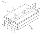
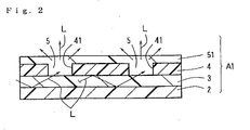
- the optical waveguide A1 for a luminescent device according to this preferred embodiment includes an under cladding layer (a planar body) 2, a core 3 formed in a predetermined pattern in a predetermined portion of the surface of the under cladding layer 2 and serving as a passageway for light beams L, and an over cladding layer 4 formed on the surface of the above-mentioned under cladding layer 2 so as to cover the core 3. Holes 41 extending to the core 3 are partially formed in the above-mentioned over cladding layer 4.
- the holes 41 are filled with a coating material 5 having a refractive index not less than that of the above-mentioned core 3. Further, in this preferred embodiment, a coating layer 51 in the form of a layer of the above-mentioned coating material 5 is formed on the surface of the over cladding layer 4.
- the refractive indices of the under cladding layer 2, core 3 and over cladding layer 4 described above are as follows: the refractive indices of the under cladding layer 2 and over cladding layer 4 are lower than the refractive index of the core 3, as in typical optical waveguides.
- a planar base 1 (as shown in Fig. 3 (a) ) for use in manufacturing the above-mentioned optical waveguide A1.
- a luminescent device see Fig. 1
- Examples of a material for the formation of the base 1 used herein include glass, quartz, silicon, resins, metal and the like.
- the thickness of the base 1 is, for example, in the range of 20 ⁇ m (for a film-like base 1) to 5 mm (for a plate-like base 1).
- a varnish prepared by dissolving a photosensitive resin in a solvent, which serves as a material for the formation of the under cladding layer 2 is applied to a predetermined region on the above-mentioned base 1.
- the application of the varnish is achieved, for example, by a spin coating method, a dipping method, a casting method, an injection method, an ink jet method and the like.
- the varnish is dried by a heating treatment at 50°C to 120°C for 10 to 30 minutes. This provides a photosensitive resin layer 2a which is to be formed into the under cladding layer 2.
- the above-mentioned photosensitive resin layer 2a is exposed to irradiation light.
- irradiation light for the above-mentioned exposure used herein include visible light, ultraviolet light, infrared light, X-rays, alpha rays, beta rays, gamma rays and the like.
- ultraviolet light is used. This is because the use of ultraviolet light achieves irradiation with large energy to provide a high rate of hardening, and an irradiation apparatus therefor is small in size and inexpensive to achieve the reduction in production costs.
- a light source of the ultraviolet light may be, for example, a low-pressure mercury-vapor lamp, a high-pressure mercury-vapor lamp, an ultra-high-pressure mercury-vapor lamp and the like.
- the dose of the ultraviolet light is typically 10 to 10000 mJ/cm 2 , preferably 50 to 3000 mJ/cm 2 .
- a heating treatment is performed to complete a photoreaction.
- This heating treatment is performed at 80°C to 250°C, preferably at 100°C to 200°C, for 10 seconds to two hours, preferably for five minutes to one hour.
- the thickness of the under cladding layer 2 is typically in the range of 1 to 50 ⁇ m, preferably in the range of 5 to 30 ⁇ m.
- a photosensitive resin layer 3a which is to be formed into the core 3 is formed on the surface of the above-mentioned under cladding layer 2.
- the formation of this photosensitive resin layer 3a is carried out in a manner similar to the method for the formation of the photosensitive resin layer 2a formed into the under cladding layer 2 described with reference to Fig. 3(a) .
- a material for the formation of the core 3 used herein is a material having a refractive index higher than the refractive indices of the materials for the formation of the above-mentioned under cladding layer 2 and the over cladding layer 4 to be described later (with reference to Fig. 3(d) ).
- This adjustment of the refractive indices may be made, for example, by adjusting the selection of the types of the materials for the formation of the above-mentioned under cladding layer 2, core 3 and over cladding layer 4, and the composition ratio thereof.
- an exposure mask formed with an opening pattern corresponding to the pattern of the core 3 is placed over the above-mentioned photosensitive resin layer 3a. Then, the above-mentioned photosensitive resin layer 3a is exposed to irradiation light through the exposure mask. Thereafter, a heating treatment is performed. The exposure and the heating treatment are carried out in a manner similar to the method for the formation of the under cladding layer 2 described with reference to Fig. 3(a) .
- the above-mentioned development employs, for example, an immersion method, a spray method, a puddle method and the like.
- Examples of the developing solution used herein include an organic solvent, an organic solvent containing an alkaline aqueous solution, and the like.
- the developing solution and conditions for the development are selected as appropriate depending on the composition of a photosensitive resin composition.
- the developing solution in the remaining photosensitive resin layer 3a formed in the pattern of the core 3 is removed by a heating treatment.
- This heating treatment is typically performed at 80°C to 120°C for 10 to 30 minutes.
- the remaining photosensitive resin layer 3a formed in the pattern of the above-mentioned core 3 is formed into the core 3.
- the thickness of the core 3 (the photosensitive resin layer 3a) is typically in the range of 20 to 150 ⁇ m, preferably in the range of 40 to 100 ⁇ m.
- the width of the core 3 is typically in the range of 10 to 500 ⁇ m, preferably in the range of 20 to 300 ⁇ m.
- a photosensitive resin layer 4a which is to be formed into the over cladding layer 4 (with reference to Fig. 3(d) ) is formed on the surface of the above-mentioned under cladding layer 2 so as to cover the above-mentioned core 3.
- the formation of this photosensitive resin layer 4a is carried out in a manner similar to the method for the formation of the photosensitive resin layer 2a formed into the under cladding layer 2 described with reference to Fig. 3 (a) .
- an exposure mask formed with an opening pattern corresponding to the pattern of the over cladding layer 4 (with reference to Fig. 3(d) ) is placed over the above-mentioned photosensitive resin layer 4a. Then, the above-mentioned photosensitive resin layer 4a is exposed to irradiation light through the exposure mask. Thereafter, a heating treatment is performed. The exposure and the heating treatment are carried out in a manner similar to the method for the formation of the under cladding layer 2 described with reference to Fig. 3(a) .
- the pattern of the above-mentioned over cladding layer 4 (the opening pattern of the exposure mask) is a pattern such that a portion except where the above-mentioned holes 41 (see Fig. 1 ) are to be formed is formed into the over cladding layer 4, as shown in Fig. 3(d) .
- a developing solution to dissolve away an unexposed portion of the above-mentioned photosensitive resin layer 4a, thereby forming the photosensitive resin layer 4a remaining on the surfaces of the under cladding layer 2 and core 3 into the pattern of the above-mentioned over cladding layer 4.
- voids resulting from the removal of the above-mentioned unexposed portion are formed into the holes 41 extending to the core 3.
- the developing solution in the remaining photosensitive resin layer 4a is removed by a heating treatment.
- the above-mentioned development and the heating treatment are carried out in a manner similar to the method for the formation of the core 3 described with reference to Fig.
- the remaining photosensitive resin layer 4a formed in the pattern of the above-mentioned over cladding layer 4 is formed into the over cladding layer 4.
- the thickness of the over cladding layer 4 (the photosensitive resin layer 4a) (a thickness as measured from the surface of the core 3) is typically in the range of 3 to 40 ⁇ m, preferably in the range of 5 to 10 ⁇ m.
- Examples of the opening shape of the above-mentioned holes (the voids resulting from the removal of the unexposed portion of the above-mentioned photosensitive resin layer 4a) 41 are a circular shape, a polygonal shape, a linear shape along the core 3 and the like.
- the dimensions of the holes 41 are as follows: typically, the width thereof is in the range of 50 to 5000 ⁇ m and the length thereof is 50 to 5000 ⁇ m; preferably, the width thereof is in the range of 100 to 3000 ⁇ m and the length thereof is 100 to 3000 ⁇ m.
- a varnish prepared by dissolving a resin and the like to be described below in a solvent, which serves as a material for the formation of the coating material 5 is applied to the surface of the above-mentioned over cladding layer 4.
- the above-mentioned holes (the voids resulting from the removal of the unexposed portion of the above-mentioned photosensitive resin layer 4a) 41 are filled with the varnish.
- the application of the varnish is achieved, for example, by a spin coating method, a dipping method, a casting method, an injection method, an ink jet method and the like.
- an appropriate method heat treating treatment, irradiation with ultraviolet light or the like is executed to harden the material for the formation of the above-mentioned coating material 5, thereby forming the coating material 5 and the coating layer 51.
- the thickness of the coating layer 51 (a thickness as measured from the surface of the core 3) is typically in the range of 5 to 100 ⁇ m, preferably in the range of 10 to 50 ⁇ m.
- the material of the above-mentioned coating material 5 used herein is required only to have a refractive index not less than that of the core 3.
- Examples of the material of the above-mentioned coating material 5 used herein include resins similar to those for the core 3, thermosetting resins, thermoplastic resins, engineering plastics, radiation curable resins and the like.
- Examples of the above-mentioned thermosetting resins include phenolic resins, urea resins, imides, polyimide resins, melamine resins, unsaturated polyesters, diallyl phthalate resins, xylene resins, alkyl benzene resins, epoxy resins, epoxy acrylate resins, silicon resins and the like.
- thermoplastic resins examples include fluororesins, vinyl chloride resins, vinylidene chloride resins, polyethylenes, chlorinated polyolefins, polypropylenes, modified polyolefins, polyvinyl acetates, ethylene-ethyl acrylate copolymers, polystyrenes, ABS resins, polyamides, (meth)acrylic resins, polyacetals, polycarbonates, cellulose-based resins, polyvinyl alcohols and the like.
- Examples of the above-mentioned engineering plastics include polyimides, polycarbodiimides, ionomer resins, polyphenylene oxides, polymethylpentenes, poly-allyl sulfones, poly-allyl ethers, polyphenylene sulfides, polysulfones, polyethylene terephthalates, polybutylene terephthalates, polytetramethylene terephthalates and the like.
- Examples of the above-mentioned radiation curable resins include ultraviolet curable resins, electron beam curable resins and the like.
- the optical waveguide A1 for a luminescent device including the under cladding layer 2, the core 3, the over cladding layer 4, the coating material 5 and the coating layer 51 is formed on the base 1.
- the above-mentioned optical waveguide A1 for a luminescent device may be used after being removed from the base 1 or be used together with the base 1 without being removed.
- the lower surface of the base 1 is initially brought into contact with a vacuum suction stage (not shown), and the base 1 is fixed thereon by air suction.
- a vacuum suction machine adheres to the upper surface of the coating layer 51 under suction to lift an adhering portion thereof in this state. This removes the under cladding layer 2 of the optical waveguide A1 for a luminescent device from the base 1, with the coating material 5, the over cladding layer 4, the core 3 and the under cladding layer 2 as well as the coating layer 51 bonded together.
- the adhesive force between the base 1 and the under cladding layer 2 is smaller than the adhesive forces between the coating layer 51 and the over cladding layer 4, between the over cladding layer 4 and the core 3 and between the over cladding layer 4 and the under cladding layer 2 because of the materials thereof.
- the above-mentioned process easily accomplish the removal.
- the above-mentioned optical waveguide A1 for a luminescent device may be used as a luminescent device by connecting a light source to an end of the core 3 and providing a control circuit for turning the light source on and off, a power supply and the like.
- an incoming call is indicated by the light emission from the above-mentioned optical waveguide A1 for a luminescent device when the above-mentioned optical waveguide A1 for a luminescent device is affixed to a peripheral side surface of a mobile device M and the like as shown in Fig. 4(a) or affixed to the front surface of the mobile device M and the like as shown in Fig.
- the above-mentioned optical waveguide A1 for a luminescent device is affixed so that the longitudinal direction of the core 3 extends along the periphery of the side surfaces of the mobile device M and the like, and the optical waveguide A1 for a luminescent device is shown as thicker for the sake of clarity.
- the core 3 is in the form of a ring as seen in plan view, and the core 3 is also shown as thicker.
- the reference character B designates a light emission controller including the above-mentioned light source, control circuit and the like.
- the light for emission is preferably visible light.
- the source of the light include a light-emitting diode, a semiconductor laser and the like. The use of a plurality of light sources having different light colors allows changes in the color pattern of the light to be emitted.
- Fig. 5 shows a second preferred embodiment of the optical waveguide for a luminescent device according to the present invention.
- the optical waveguide A2 for a luminescent device according to the second preferred embodiment light scattering particles 6 are dispersed in the coating material 5 which fills the above-mentioned holes 41.
- the second preferred embodiment is similar to the first preferred embodiment described above.
- Like reference numerals and characters are used to designate parts similar to those of the first preferred embodiment.
- the light beams L coming into the coating material 5 are refracted or reflected by the above-mentioned light scattering particles 6 and are scattered.
- the light beams L being scattered are emitted to the outside. This improves the visibility of the emitted light beams L.
- the above-mentioned light scattering particles 6 include silica particles, alumina particles, silicone particles, titania particles, zirconia particles, plastic particles, liquid crystal particles, air bubbles (hollow particles) and the like. These are used either alone or in combination.
- the average particle size of the light scattering particles 6 is in the range of 0.1 to 50 ⁇ m from the viewpoint of the excellent light scattering property thereof.
- the average particle size is the average of the particle diameters of ten arbitrary light scattering particles 6.
- the particle diameter of each of the light scattering particles 6 is the maximum diameter thereof measured under a microscope.
- a method of dispersing the above-mentioned light scattering particles 6 in the coating material 5 includes previously mixing the above-mentioned light scattering particles 6 in the material for the formation of the coating material 5, and applying the material for the formation of the coating material 5 in a manner as mentioned above.
- the mixing ratio is preferably not greater than 30 parts by volume of the light scattering particles 6 per 100 parts by volume of the material for the formation of the coating material 5 from the viewpoint of the excellent light scattering property thereof.
- Fig. 6 shows a third preferred embodiment of the optical waveguide for a luminescent device according to the present invention.
- the surface of the coating layer 51 from which the light beams L are emitted is an uneven rough surface 52.
- the third preferred embodiment is similar to the first preferred embodiment described above.
- Like reference numerals and characters are used to designate parts similar to those of the first preferred embodiment.
- the light beams L emitted from the surface of the coating layer 51 are refracted in random directions by the unevenness of the surface of the coating layer 51 and are scattered. This improves the visibility of the emitted light beams L. Since surface portions of the coating layer 51 from which the light beams L are emitted are only the portions of the coating layer 51 positioned over the holes 41 and their peripheral portions, only the surface portions of the coating layer 51 from which the light beams L are emitted may be formed as the uneven rough surface 52.
- Exemplary methods of forming the surface of the above-mentioned coating layer 51 as the uneven rough surface 52 include a method of scratching the surface of the coating layer 51 with sandpaper and the like after the coating layer 51 is formed, a laser processing method, a method of molding with a die, and the like.
- Fig. 7 shows a fourth preferred embodiment of the optical waveguide for a luminescent device according to the present invention.
- the optical waveguide A4 for a luminescent device according to the fourth preferred embodiment is a combination of the second preferred embodiment (see Fig. 5 ) and the third preferred embodiment (see Fig. 6 ) described above.
- the light scattering particles 6 are dispersed in the coating material 5 which fills the above-mentioned holes 41, and the surface of the coating layer 51 is the uneven rough surface 52.
- the fourth preferred embodiment is similar to the second and third preferred embodiments described above.
- Like reference numerals and characters are used to designate parts similar to those of the second and third preferred embodiments.
- the optical waveguide A4 for a luminescent device produces synergistic effects between the light scattering particles 6 and the uneven rough surface 52 to increase the scattering of the emitted light beams L, thereby further improving the visibility of the light beams L.
- Fig. 8 shows a fifth preferred embodiment of the optical waveguide for a luminescent device according to the present invention.
- the coating material 5 in the above-mentioned second preferred embodiment is formed only in the holes 41 formed in the over cladding layer 4, and the coating layer 51 is not formed on the surface of the over cladding layer 4.
- the fifth preferred embodiment is similar to the second preferred embodiment described above.
- Like reference numerals and characters are used to designate parts similar to those of the second preferred embodiment.
- An exemplary method of forming the coating material 5 only in the above-mentioned holes 41 in the fifth preferred embodiment includes a method of potting the material for the formation of the coating material 5 into the above-mentioned holes 41 (a method of filling the holes 41 with the material fed from a tip of a thin tube).
- This provides the surface of the coating material 5 in the form of part of a spherical surface or a convexly curved surface 53 close thereto.
- the light beams L emitted from the surface of the coating material 5 are refracted in various directions by the convexly curved surface 53 at the surface of the coating material 5 and are scattered. This improves the visibility of the emitted light beams L.
- the coating material 5 may be formed only in the holes 41 formed in the over cladding layer 4 in a manner similar to the fifth preferred embodiment.
- a photosensitive resin is used as the material of the over cladding layer 4, and is exposed to light and then developed in the above-mentioned preferred embodiments.
- the over cladding layer 4 formed with the holes 41 for the formation of the coating material 5 may be formed using other resins as the material thereof by laser processing, etching, printing, die molding and the like.
- a photosensitive resin is used as the material of the under cladding layer 2, and the formation of the under cladding layer 2 is accomplished by exposure to light and development in the above-mentioned preferred embodiments.
- a thermosetting resin such as polyimide resin, epoxy resin and the like may be used as the material of the under cladding layer 2
- the under cladding layer 2 may be formed by applying a varnish prepared by dissolving the thermosetting resin in a solvent, and thereafter performing a heating treatment (typically at 300°C to 400°C for 60 to 180 minutes) to harden the thermosetting resin, or by other methods.
- a photosensitive resin is used to form the under cladding layer 2 in the above-mentioned preferred embodiments.
- other materials may be used.
- a resin film may be used as the under cladding layer 2.
- a substrate with a metal film or a metal thin film formed on the surface thereof may be used in place of the under cladding layer 2 so that the surface of the metal material functions as a surface for reflecting the light beams L propagating through the core 3.
- a material for formation of an under cladding layer and an over cladding layer was prepared by mixing 35 parts by weight of bisphenoxyethanol fluorene glycidyl ether (component A) represented by the following general formula (1), 40 parts by weight of 3',4'-epoxycyclohexylmethyl-3,4-epoxycyclohexane carboxylate which is an alicyclic epoxy resin (CELLOXIDE 2021P manufactured by Daicel Chemical Industries,Ltd.)(Component B), 25 parts by weight of (3',4'-epoxycyclohexane)methyl-3',4'-epoxycyclohexyl-carboxylate(CELLOXIDE 2081 manufactured by Daicel Chemical Industries, Ltd.) (Component C), and 2 parts by weight of a 50% propione carbonate solution of 4,4'-bis[di( ⁇ -hydroxyethoxy)phenylsulfinio]phenylsulfide-bis-hexafluoroanti
- a material for formation of a core was prepared by dissolving 70 parts by weight of the aforementioned component A, 30 parts by weight of 1,3,3-tris ⁇ 4-[2-(3-oxetanyl)]butoxyphenyl ⁇ butane and one part by weight of the aforementioned component D in 28 parts by weight of ethyl lactate.
- Coating Layer Material for Formation of Coating Material
- the material for the formation of the above-mentioned under cladding layer was applied to the surface of a polyethylene naphthalate (PEN) film [100 mm x 100 mm x 188 ⁇ m (thick)] by a spin coating method. Thereafter, exposure by the use of irradiation with ultraviolet light at 2000 mJ/cm 2 was performed. Subsequently, a heating treatment was performed at 100°C for 15 minutes to form the under cladding layer. The thickness of this under cladding layer was 25 ⁇ m when measured with a contact-type film thickness meter. The refractive index of this under cladding layer at a wavelength of 830 nm was 1.542.
- PEN polyethylene naphthalate
- the material for the formation of the above-mentioned core was applied to the surface of the above-mentioned under cladding layer by a spin coating method. Thereafter, a drying process was performed at 100°C for 15 minutes. Next, a synthetic quartz chrome mask (exposure mask) formed with an opening pattern identical in shape with the pattern of the core was placed over the resulting core material. Then, exposure by the use of irradiation with ultraviolet light at 4000 mJ/cm 2 was performed by a contact exposure method from over the mask. Thereafter, a heating treatment was performed at 120°C for 15 minutes. Next, development was carried out using an aqueous solution of ⁇ -butyrolactone to dissolve away an unexposed portion.
- the dimensions of the core in cross section were 100 ⁇ m in width x 80 ⁇ m in height when measured with an SEM.
- the refractive index of the core at a wavelength of 830 nm was 1.588.
- the material for the formation of the above-mentioned over cladding layer was applied to the surface of the above-mentioned under cladding layer by a spin coating method so as to cover the above-mentioned core.
- a synthetic quartz chrome mask exposure mask
- exposure mask formed with an opening pattern identical in shape with the pattern of the over cladding layer was positioned over the material for the formation of the over cladding layer.
- exposure by the use of irradiation with ultraviolet light at 2000 mJ/cm 2 was performed by a contact exposure method from above the mask.
- a heating treatment was performed at 120°C for 15 minutes.
- the thickness of the over cladding layer (a thickness as measured from the surface of the core) was 5 ⁇ m when measured with a contact-type film thickness meter.
- the refractive index of the over cladding layer at a wavelength of 830 nm was 1.542.
- the material for the formation of the above-mentioned coating material (the coating layer) was applied to the surface of the above-mentioned over cladding layer by a spin coating method. Then, exposure by the use of irradiation with ultraviolet light at 4000 mJ/cm 2 was performed from over the material for the formation of the coating material (the coating layer). Thereafter, a heating treatment was performed at 120°C for 15 minutes to form the coating material filling the above-mentioned holes and the coating layer on the surface of the over cladding layer. The thickness of the coating layer (a thickness as measured from the surface of the over cladding layer) was 6 ⁇ m when measured with a contact-type film thickness meter.
- the refractive index of the coating material (the coating layer) at a wave length of 830 nm was 1.588 because a base material for the formation of the coating material (the coating layer) was similar to that of the above-mentioned core. In this manner, an optical waveguide for a luminescent device was provided.
- Example 2 A mixture of 5 parts by volume of fine particles of silicone resin (having a refractive index of 1.43) having an average particle size of 0.7 ⁇ m as light scattering particles in 100 parts by volume of the material for the formation of the above-mentioned core was used as the material for the formation of the coating material (the coating layer) in Example 1 described above. Except for this, Example 2 was similar to Example 1 described above. In this manner, an optical waveguide for a luminescent device was produced.
- Example 3 was similar to Example 1 described above. In this manner, an optical waveguide for a luminescent device was produced.
- Example 2 the surface of the coating material (the coating layer) was roughened in a manner similar to that in Example 3 described above. Except for this, Example 4 was similar to Example 2 described above. In this manner, an optical waveguide for a luminescent device was produced.
- Example 2 the potting of the material for the formation of the coating material only in the holes formed in the over cladding layer was carried out to fill only the holes with the coating material.
- the coating layer was not formed on the surface of the over cladding layer.
- Example 5 was similar to Example 1 described above. In this manner, an optical waveguide for a luminescent device was produced.
- a light receiving surface was formed by dicing near an end of the core.
- a manual alignment stage was used to align a red light emitting diode having a wavelength of 660 nm so that light enters the core. Thereafter, the red light emitting diode was fixed with an ultraviolet curable resin. Then, when light was emitted from the red light emitting diode, the emission of the red light from the surface portion of the coating layer over the coating material (the holes formed in the over cladding layer) was observed in all Examples.
- the light emission in Examples 2 through 5 was better in visibility by visual observation. Further, the light emission in Examples 4 and 5 was much better in visibility by visual observation.
Landscapes
- Physics & Mathematics (AREA)
- Engineering & Computer Science (AREA)
- General Physics & Mathematics (AREA)
- Optics & Photonics (AREA)
- Microelectronics & Electronic Packaging (AREA)
- Signal Processing (AREA)
- Optical Integrated Circuits (AREA)
Abstract
Description
- The present invention relates to an optical waveguide for a luminescent device for ornamental or other purposes, and a manufacturing method thereof.
- Heretofore, a light emitting board using an optical waveguide has been proposed as a light emitting board which can be used for ornamental objects and the like (see Japanese Patent No.
2814684 - In the above-mentioned light emitting board, however, the low refractive portion (the over cladding layer) having the refractive index lower than that of the light guiding portion (the core) covers the light guiding portion (the core) through which the light beams propagate. It is therefore difficult for the light beams propagating through the above-mentioned light guiding portion (the core) to travel toward the low refractive portion (the over cladding layer). In other words, the above-mentioned light emitting board is low in outward light emission efficiency.
- In view of the foregoing, it is an object of the present invention to provide an optical waveguide for a luminescent device capable of efficiently leading light beams propagating through a core outwardly to cause light emission, and a manufacturing method thereof.
- To accomplish the above-mentioned object, a first aspect of the present invention is intended for an optical waveguide for a luminescent device comprising: a planar body, a core formed in a predetermined portion of a surface of the body, and an over cladding layer formed on the surface of said body so as to cover the core, wherein said over cladding layer includes a hole formed in a predetermined portion thereof and extending to the core, and wherein said hole is filled with a coating material having a refractive index not less than that of said core.
- A second aspect of the present invention is intended for a method of manufacturing the above-mentioned optical waveguide for a luminescent device, comprising the steps of: forming a core in a predetermined portion of a surface of a planar body; forming a photosensitive resin layer on the surface of said body and then exposing the photosensitive resin layer to light except where a hole is to be formed to form an exposed portion of the photosensitive resin layer into an over cladding layer; removing said unexposed portion to form a void resulting from the removal into the hole; and potting a coating material having a refractive index not less than that of said core into the hole and then hardening the coating material to fill said hole with the coating material.
- In the optical waveguide for a luminescent device according to the present invention, the hole extending to the core is formed in the predetermined portion of the over cladding layer, and the refractive index of the coating material filling the hole is not less than that of the above-mentioned core. Thus, at least some of the light beams propagating through the core travel into the coating material without resistance and are then emitted outwardly from the surface of the coating material. In other words, the optical waveguide for a luminescent device according to the present invention is capable of efficiently leading at least some of the light beams propagating through the core outwardly to cause light emission.
- In particular, when light scattering particles are dispersed in the coating material filling the above-mentioned hole, the light beams passing through the coating material are refracted or reflected by the light scattering particles and are scattered. The light beams being scattered are emitted to the outside. This improves the visibility of the emitted light beams.
- Additionally, when the surface of the coating material filling the above-mentioned hole is in the form of an uneven rough surface, the light beams emitted from the surface of the coating material is refracted in random directions by the uneven rough surface and are scattered. This improves the visibility of the emitted light beams.
- The method of manufacturing the optical waveguide for a luminescent device according to the present invention includes: exposing the photosensitive resin layer formed so as to cover the core to light, except where the hole is to be formed, to form the exposed portion of the photosensitive resin layer into the over cladding layer; removing the unexposed portion to form the void resulting from the removal into the hole; and potting the coating material having the refractive index not less than that of the core into the hole and then hardening the coating material to fill the above-mentioned hole with the coating material. Thus, the method provides the optical waveguide for a luminescent device according to the present invention capable of efficiently leading at least some of the light beams propagating through the core outwardly to cause light emission.
-
-
Fig. 1 is a perspective view schematically showing a first preferred embodiment of an optical waveguide for a luminescent device according to the present invention. -
Fig. 2 is a sectional view taken along the line X-X ofFig. 1 . -
Figs. 3(a) to (e) are views schematically illustrating a method of manufacturing the above-mentioned optical waveguide for a luminescent device. -
Figs. 4(a) and (b) are views schematically illustrating examples of the use of the above-mentioned optical waveguide for a luminescent device. -
Fig. 5 is a sectional view schematically showing a second preferred embodiment of the optical waveguide for a luminescent device according to the present invention. -
Fig. 6 is a sectional view schematically showing a third preferred embodiment of the optical waveguide for a luminescent device according to the present invention. -
Fig. 7 is a sectional view schematically showing a fourth preferred embodiment of the optical waveguide for a luminescent device according to the present invention. -
Fig. 8 is a sectional view schematically showing a fifth preferred embodiment of the optical waveguide for a luminescent device according to the present invention. - Preferred embodiments according to the present invention will now be described in detail with reference to the drawings.
-
Figs. 1 and2 show a first preferred embodiment of an optical waveguide for a luminescent device according to the present invention. The optical waveguide A1 for a luminescent device according to this preferred embodiment includes an under cladding layer (a planar body) 2, acore 3 formed in a predetermined pattern in a predetermined portion of the surface of the under claddinglayer 2 and serving as a passageway for light beams L, and an over claddinglayer 4 formed on the surface of the above-mentioned undercladding layer 2 so as to cover thecore 3.Holes 41 extending to thecore 3 are partially formed in the above-mentioned overcladding layer 4. Theholes 41 are filled with acoating material 5 having a refractive index not less than that of the above-mentionedcore 3. Further, in this preferred embodiment, acoating layer 51 in the form of a layer of the above-mentionedcoating material 5 is formed on the surface of the over claddinglayer 4. The refractive indices of the undercladding layer 2,core 3 and overcladding layer 4 described above are as follows: the refractive indices of the undercladding layer 2 and overcladding layer 4 are lower than the refractive index of thecore 3, as in typical optical waveguides. - When light beams L are propagated through the
core 3 of the above-mentioned optical waveguide A1 for a luminescent device, at least some of the light beams L propagating through thecore 3 travel into thecoating material 5 filling the above-mentionedholes 41 without resistance and are then emitted outwardly from surface portions of thecoating layer 51 positioned over theholes 41 and their peripheral portions because the refractive index of thecoating material 5 is not less than that of thecore 3. - An example of a method of manufacturing such an optical waveguide A1 for a luminescent device will be described.
- First, a planar base 1 (as shown in
Fig. 3 (a) ) for use in manufacturing the above-mentioned optical waveguide A1. for a luminescent device (seeFig. 1 ) is prepared. Examples of a material for the formation of thebase 1 used herein include glass, quartz, silicon, resins, metal and the like. The thickness of thebase 1 is, for example, in the range of 20 µm (for a film-like base 1) to 5 mm (for a plate-like base 1). - Next, as shown in
Fig. 3(a) , a varnish prepared by dissolving a photosensitive resin in a solvent, which serves as a material for the formation of the undercladding layer 2, is applied to a predetermined region on the above-mentionedbase 1. The application of the varnish is achieved, for example, by a spin coating method, a dipping method, a casting method, an injection method, an ink jet method and the like. Then, the varnish is dried by a heating treatment at 50°C to 120°C for 10 to 30 minutes. This provides aphotosensitive resin layer 2a which is to be formed into the under claddinglayer 2. - Next, the above-mentioned
photosensitive resin layer 2a is exposed to irradiation light. Examples of the irradiation light for the above-mentioned exposure used herein include visible light, ultraviolet light, infrared light, X-rays, alpha rays, beta rays, gamma rays and the like. Preferably, ultraviolet light is used. This is because the use of ultraviolet light achieves irradiation with large energy to provide a high rate of hardening, and an irradiation apparatus therefor is small in size and inexpensive to achieve the reduction in production costs. A light source of the ultraviolet light may be, for example, a low-pressure mercury-vapor lamp, a high-pressure mercury-vapor lamp, an ultra-high-pressure mercury-vapor lamp and the like. The dose of the ultraviolet light is typically 10 to 10000 mJ/cm2, preferably 50 to 3000 mJ/cm2. - After the above-mentioned exposure, a heating treatment is performed to complete a photoreaction. This heating treatment is performed at 80°C to 250°C, preferably at 100°C to 200°C, for 10 seconds to two hours, preferably for five minutes to one hour. This forms the above-mentioned
photosensitive resin layer 2a into the under claddinglayer 2. The thickness of the under cladding layer 2 (thephotosensitive resin layer 2a) is typically in the range of 1 to 50 µm, preferably in the range of 5 to 30 µm. - Next, as shown in
Fig. 3(b) , aphotosensitive resin layer 3a which is to be formed into thecore 3 is formed on the surface of the above-mentioned undercladding layer 2. The formation of thisphotosensitive resin layer 3a is carried out in a manner similar to the method for the formation of thephotosensitive resin layer 2a formed into the undercladding layer 2 described with reference toFig. 3(a) . A material for the formation of thecore 3 used herein is a material having a refractive index higher than the refractive indices of the materials for the formation of the above-mentioned undercladding layer 2 and the overcladding layer 4 to be described later (with reference toFig. 3(d) ). This adjustment of the refractive indices may be made, for example, by adjusting the selection of the types of the materials for the formation of the above-mentioned undercladding layer 2,core 3 and overcladding layer 4, and the composition ratio thereof. - Next, an exposure mask formed with an opening pattern corresponding to the pattern of the
core 3 is placed over the above-mentionedphotosensitive resin layer 3a. Then, the above-mentionedphotosensitive resin layer 3a is exposed to irradiation light through the exposure mask. Thereafter, a heating treatment is performed. The exposure and the heating treatment are carried out in a manner similar to the method for the formation of theunder cladding layer 2 described with reference toFig. 3(a) . - Subsequently, development is performed using a developing solution to dissolve away an unexposed portion of the above-mentioned
photosensitive resin layer 3a, thereby forming thephotosensitive resin layer 3a remaining on the undercladding layer 2 into the pattern of thecore 3. The above-mentioned development employs, for example, an immersion method, a spray method, a puddle method and the like. Examples of the developing solution used herein include an organic solvent, an organic solvent containing an alkaline aqueous solution, and the like. The developing solution and conditions for the development are selected as appropriate depending on the composition of a photosensitive resin composition. - After the above-mentioned development, the developing solution in the remaining
photosensitive resin layer 3a formed in the pattern of thecore 3 is removed by a heating treatment. This heating treatment is typically performed at 80°C to 120°C for 10 to 30 minutes. Thus, the remainingphotosensitive resin layer 3a formed in the pattern of the above-mentionedcore 3 is formed into thecore 3. The thickness of the core 3 (thephotosensitive resin layer 3a) is typically in the range of 20 to 150 µm, preferably in the range of 40 to 100 µm. The width of thecore 3 is typically in the range of 10 to 500 µm, preferably in the range of 20 to 300 µm. - Then, as shown in
Fig. 3(c) , aphotosensitive resin layer 4a which is to be formed into the over cladding layer 4 (with reference toFig. 3(d) ) is formed on the surface of the above-mentioned undercladding layer 2 so as to cover the above-mentionedcore 3. The formation of thisphotosensitive resin layer 4a is carried out in a manner similar to the method for the formation of thephotosensitive resin layer 2a formed into the undercladding layer 2 described with reference toFig. 3 (a) . - Next, an exposure mask formed with an opening pattern corresponding to the pattern of the over cladding layer 4 (with reference to
Fig. 3(d) ) is placed over the above-mentionedphotosensitive resin layer 4a. Then, the above-mentionedphotosensitive resin layer 4a is exposed to irradiation light through the exposure mask. Thereafter, a heating treatment is performed. The exposure and the heating treatment are carried out in a manner similar to the method for the formation of theunder cladding layer 2 described with reference toFig. 3(a) . The pattern of the above-mentioned over cladding layer 4 (the opening pattern of the exposure mask) is a pattern such that a portion except where the above-mentioned holes 41 (seeFig. 1 ) are to be formed is formed into the overcladding layer 4, as shown inFig. 3(d) . - Subsequently, as shown in
Fig. 3(d) , development is performed using a developing solution to dissolve away an unexposed portion of the above-mentionedphotosensitive resin layer 4a, thereby forming thephotosensitive resin layer 4a remaining on the surfaces of theunder cladding layer 2 andcore 3 into the pattern of the above-mentioned overcladding layer 4. At this time, voids resulting from the removal of the above-mentioned unexposed portion are formed into theholes 41 extending to thecore 3. Thereafter, the developing solution in the remainingphotosensitive resin layer 4a is removed by a heating treatment. The above-mentioned development and the heating treatment are carried out in a manner similar to the method for the formation of thecore 3 described with reference toFig. 3(b) . Thus, the remainingphotosensitive resin layer 4a formed in the pattern of the above-mentioned overcladding layer 4 is formed into the overcladding layer 4. The thickness of the over cladding layer 4 (thephotosensitive resin layer 4a) (a thickness as measured from the surface of the core 3) is typically in the range of 3 to 40 µm, preferably in the range of 5 to 10 µm. Examples of the opening shape of the above-mentioned holes (the voids resulting from the removal of the unexposed portion of the above-mentionedphotosensitive resin layer 4a) 41 are a circular shape, a polygonal shape, a linear shape along thecore 3 and the like. The dimensions of theholes 41 are as follows: typically, the width thereof is in the range of 50 to 5000 µm and the length thereof is 50 to 5000 µm; preferably, the width thereof is in the range of 100 to 3000 µm and the length thereof is 100 to 3000 µm. - Then, as shown in
Fig. 3(e) , a varnish prepared by dissolving a resin and the like to be described below in a solvent, which serves as a material for the formation of thecoating material 5, is applied to the surface of the above-mentioned overcladding layer 4. At the same time, the above-mentioned holes (the voids resulting from the removal of the unexposed portion of the above-mentionedphotosensitive resin layer 4a) 41 are filled with the varnish. The application of the varnish is achieved, for example, by a spin coating method, a dipping method, a casting method, an injection method, an ink jet method and the like. Next, depending on the material of the above-mentionedcoating material 5 to be described below, an appropriate method (heating treatment, irradiation with ultraviolet light or the like) is executed to harden the material for the formation of the above-mentionedcoating material 5, thereby forming thecoating material 5 and thecoating layer 51. The thickness of the coating layer 51 (a thickness as measured from the surface of the core 3) is typically in the range of 5 to 100 µm, preferably in the range of 10 to 50 µm. - The material of the above-mentioned
coating material 5 used herein is required only to have a refractive index not less than that of thecore 3. Examples of the material of the above-mentionedcoating material 5 used herein include resins similar to those for thecore 3, thermosetting resins, thermoplastic resins, engineering plastics, radiation curable resins and the like. Examples of the above-mentioned thermosetting resins include phenolic resins, urea resins, imides, polyimide resins, melamine resins, unsaturated polyesters, diallyl phthalate resins, xylene resins, alkyl benzene resins, epoxy resins, epoxy acrylate resins, silicon resins and the like. Examples of the above-mentioned thermoplastic resins include fluororesins, vinyl chloride resins, vinylidene chloride resins, polyethylenes, chlorinated polyolefins, polypropylenes, modified polyolefins, polyvinyl acetates, ethylene-ethyl acrylate copolymers, polystyrenes, ABS resins, polyamides, (meth)acrylic resins, polyacetals, polycarbonates, cellulose-based resins, polyvinyl alcohols and the like. Examples of the above-mentioned engineering plastics include polyimides, polycarbodiimides, ionomer resins, polyphenylene oxides, polymethylpentenes, poly-allyl sulfones, poly-allyl ethers, polyphenylene sulfides, polysulfones, polyethylene terephthalates, polybutylene terephthalates, polytetramethylene terephthalates and the like. Examples of the above-mentioned radiation curable resins include ultraviolet curable resins, electron beam curable resins and the like. - In this manner, the optical waveguide A1 for a luminescent device including the under
cladding layer 2, thecore 3, the overcladding layer 4, thecoating material 5 and thecoating layer 51 is formed on thebase 1. - Thereafter, the above-mentioned optical waveguide A1 for a luminescent device may be used after being removed from the
base 1 or be used together with thebase 1 without being removed. For the removal, the lower surface of thebase 1 is initially brought into contact with a vacuum suction stage (not shown), and thebase 1 is fixed thereon by air suction. Next, a vacuum suction machine (not shown) adheres to the upper surface of thecoating layer 51 under suction to lift an adhering portion thereof in this state. This removes the undercladding layer 2 of the optical waveguide A1 for a luminescent device from thebase 1, with thecoating material 5, the overcladding layer 4, thecore 3 and the undercladding layer 2 as well as thecoating layer 51 bonded together. The adhesive force between thebase 1 and the undercladding layer 2 is smaller than the adhesive forces between thecoating layer 51 and the overcladding layer 4, between the overcladding layer 4 and thecore 3 and between the overcladding layer 4 and the undercladding layer 2 because of the materials thereof. Thus, the above-mentioned process easily accomplish the removal. - The above-mentioned optical waveguide A1 for a luminescent device may be used as a luminescent device by connecting a light source to an end of the
core 3 and providing a control circuit for turning the light source on and off, a power supply and the like. For example, an incoming call is indicated by the light emission from the above-mentioned optical waveguide A1 for a luminescent device when the above-mentioned optical waveguide A1 for a luminescent device is affixed to a peripheral side surface of a mobile device M and the like as shown inFig. 4(a) or affixed to the front surface of the mobile device M and the like as shown inFig. 4 (b) in such a manner that thecoating layer 51 faces outward and the above-mentioned light source is turned on in response to the incoming call. InFig. 4(a) , the above-mentioned optical waveguide A1 for a luminescent device is affixed so that the longitudinal direction of thecore 3 extends along the periphery of the side surfaces of the mobile device M and the like, and the optical waveguide A1 for a luminescent device is shown as thicker for the sake of clarity. InFig. 4(b) , thecore 3 is in the form of a ring as seen in plan view, and thecore 3 is also shown as thicker. InFigs. 4(a) and (b) , the reference character B designates a light emission controller including the above-mentioned light source, control circuit and the like. When the optical waveguide A1 for a luminescent device is used as such a luminescent device, the light for emission is preferably visible light. Examples of the source of the light include a light-emitting diode, a semiconductor laser and the like. The use of a plurality of light sources having different light colors allows changes in the color pattern of the light to be emitted. -
Fig. 5 shows a second preferred embodiment of the optical waveguide for a luminescent device according to the present invention. In the optical waveguide A2 for a luminescent device according to the second preferred embodiment,light scattering particles 6 are dispersed in thecoating material 5 which fills the above-mentionedholes 41. Except for this, the second preferred embodiment is similar to the first preferred embodiment described above. Like reference numerals and characters are used to designate parts similar to those of the first preferred embodiment. - In the optical waveguide A2 for a luminescent device according to the second preferred embodiment, the light beams L coming into the
coating material 5 are refracted or reflected by the above-mentionedlight scattering particles 6 and are scattered. The light beams L being scattered are emitted to the outside. This improves the visibility of the emitted light beams L. - Examples of the above-mentioned
light scattering particles 6 include silica particles, alumina particles, silicone particles, titania particles, zirconia particles, plastic particles, liquid crystal particles, air bubbles (hollow particles) and the like. These are used either alone or in combination. Preferably, the average particle size of thelight scattering particles 6 is in the range of 0.1 to 50 µm from the viewpoint of the excellent light scattering property thereof. The average particle size is the average of the particle diameters of ten arbitrarylight scattering particles 6. The particle diameter of each of thelight scattering particles 6 is the maximum diameter thereof measured under a microscope. A method of dispersing the above-mentionedlight scattering particles 6 in thecoating material 5 includes previously mixing the above-mentionedlight scattering particles 6 in the material for the formation of thecoating material 5, and applying the material for the formation of thecoating material 5 in a manner as mentioned above. The mixing ratio is preferably not greater than 30 parts by volume of thelight scattering particles 6 per 100 parts by volume of the material for the formation of thecoating material 5 from the viewpoint of the excellent light scattering property thereof. -
Fig. 6 shows a third preferred embodiment of the optical waveguide for a luminescent device according to the present invention. In the optical waveguide A3 for a luminescent device according to the third preferred embodiment, the surface of thecoating layer 51 from which the light beams L are emitted is an unevenrough surface 52. Except for this, the third preferred embodiment is similar to the first preferred embodiment described above. Like reference numerals and characters are used to designate parts similar to those of the first preferred embodiment. - In the optical waveguide A3 for a luminescent device according to the third preferred embodiment, the light beams L emitted from the surface of the
coating layer 51 are refracted in random directions by the unevenness of the surface of thecoating layer 51 and are scattered. This improves the visibility of the emitted light beams L. Since surface portions of thecoating layer 51 from which the light beams L are emitted are only the portions of thecoating layer 51 positioned over theholes 41 and their peripheral portions, only the surface portions of thecoating layer 51 from which the light beams L are emitted may be formed as the unevenrough surface 52. - Exemplary methods of forming the surface of the above-mentioned
coating layer 51 as the unevenrough surface 52 include a method of scratching the surface of thecoating layer 51 with sandpaper and the like after thecoating layer 51 is formed, a laser processing method, a method of molding with a die, and the like. -
Fig. 7 shows a fourth preferred embodiment of the optical waveguide for a luminescent device according to the present invention. The optical waveguide A4 for a luminescent device according to the fourth preferred embodiment is a combination of the second preferred embodiment (seeFig. 5 ) and the third preferred embodiment (seeFig. 6 ) described above. Specifically, thelight scattering particles 6 are dispersed in thecoating material 5 which fills the above-mentionedholes 41, and the surface of thecoating layer 51 is the unevenrough surface 52. Except for this, the fourth preferred embodiment is similar to the second and third preferred embodiments described above. Like reference numerals and characters are used to designate parts similar to those of the second and third preferred embodiments. - The optical waveguide A4 for a luminescent device according to the fourth preferred embodiment produces synergistic effects between the
light scattering particles 6 and the unevenrough surface 52 to increase the scattering of the emitted light beams L, thereby further improving the visibility of the light beams L. -
Fig. 8 shows a fifth preferred embodiment of the optical waveguide for a luminescent device according to the present invention. In the optical waveguide A5 for a luminescent device according to the fifth preferred embodiment, thecoating material 5 in the above-mentioned second preferred embodiment (seeFig. 5 ) is formed only in theholes 41 formed in the overcladding layer 4, and thecoating layer 51 is not formed on the surface of the overcladding layer 4. Except for this, the fifth preferred embodiment is similar to the second preferred embodiment described above. Like reference numerals and characters are used to designate parts similar to those of the second preferred embodiment. - An exemplary method of forming the
coating material 5 only in the above-mentionedholes 41 in the fifth preferred embodiment includes a method of potting the material for the formation of thecoating material 5 into the above-mentioned holes 41 (a method of filling theholes 41 with the material fed from a tip of a thin tube). This provides the surface of thecoating material 5 in the form of part of a spherical surface or a convexlycurved surface 53 close thereto. The light beams L emitted from the surface of thecoating material 5 are refracted in various directions by the convexlycurved surface 53 at the surface of thecoating material 5 and are scattered. This improves the visibility of the emitted light beams L. - In the first preferred embodiment (see
Fig. 2 ), the third preferred embodiment (seeFig. 6 ) and the fourth preferred embodiment (seeFig. 7 ) described above, thecoating material 5 may be formed only in theholes 41 formed in the overcladding layer 4 in a manner similar to the fifth preferred embodiment. - In forming the
holes 41 for the formation of thecoating material 5 in the overcladding layer 4, a photosensitive resin is used as the material of the overcladding layer 4, and is exposed to light and then developed in the above-mentioned preferred embodiments. However, other materials and other methods may be used. For example, the overcladding layer 4 formed with theholes 41 for the formation of thecoating material 5 may be formed using other resins as the material thereof by laser processing, etching, printing, die molding and the like. - In forming the under
cladding layer 2, a photosensitive resin is used as the material of theunder cladding layer 2, and the formation of theunder cladding layer 2 is accomplished by exposure to light and development in the above-mentioned preferred embodiments. However, other materials and other methods may be used. For example, a thermosetting resin such as polyimide resin, epoxy resin and the like may be used as the material of theunder cladding layer 2, and the undercladding layer 2 may be formed by applying a varnish prepared by dissolving the thermosetting resin in a solvent, and thereafter performing a heating treatment (typically at 300°C to 400°C for 60 to 180 minutes) to harden the thermosetting resin, or by other methods. - Further, a photosensitive resin is used to form the under
cladding layer 2 in the above-mentioned preferred embodiments. However, other materials may be used. A resin film may be used as the undercladding layer 2. Alternatively, a substrate with a metal film or a metal thin film formed on the surface thereof may be used in place of theunder cladding layer 2 so that the surface of the metal material functions as a surface for reflecting the light beams L propagating through thecore 3. - Next, inventive examples of the present invention will be described. It should be noted that the present invention is not limited to the inventive examples.
- A material for formation of an under cladding layer and an over cladding layer was prepared by mixing 35 parts by weight of bisphenoxyethanol fluorene glycidyl ether (component A) represented by the following general formula (1), 40 parts by weight of 3',4'-epoxycyclohexylmethyl-3,4-epoxycyclohexane carboxylate which is an alicyclic epoxy resin (CELLOXIDE 2021P manufactured by Daicel Chemical Industries,Ltd.)(Component B), 25 parts by weight of (3',4'-epoxycyclohexane)methyl-3',4'-epoxycyclohexyl-carboxylate(CELLOXIDE 2081 manufactured by Daicel Chemical Industries, Ltd.) (Component C), and 2 parts by weight of a 50% propione carbonate solution of 4,4'-bis[di(β-hydroxyethoxy)phenylsulfinio]phenylsulfide-bis-hexafluoroantimonate (component D).

- A material for formation of a core was prepared by dissolving 70 parts by weight of the aforementioned component A, 30 parts by weight of 1,3,3-tris{4-[2-(3-oxetanyl)]butoxyphenyl}butane and one part by weight of the aforementioned component D in 28 parts by weight of ethyl lactate.
- A material similar to the material for the formation of the above-mentioned core was prepared.
- The material for the formation of the above-mentioned under cladding layer was applied to the surface of a polyethylene naphthalate (PEN) film [100 mm x 100 mm x 188 µm (thick)] by a spin coating method. Thereafter, exposure by the use of irradiation with ultraviolet light at 2000 mJ/cm2 was performed. Subsequently, a heating treatment was performed at 100°C for 15 minutes to form the under cladding layer. The thickness of this under cladding layer was 25 µm when measured with a contact-type film thickness meter. The refractive index of this under cladding layer at a wavelength of 830 nm was 1.542.
- Next, the material for the formation of the above-mentioned core was applied to the surface of the above-mentioned under cladding layer by a spin coating method. Thereafter, a drying process was performed at 100°C for 15 minutes. Next, a synthetic quartz chrome mask (exposure mask) formed with an opening pattern identical in shape with the pattern of the core was placed over the resulting core material. Then, exposure by the use of irradiation with ultraviolet light at 4000 mJ/cm2 was performed by a contact exposure method from over the mask. Thereafter, a heating treatment was performed at 120°C for 15 minutes. Next, development was carried out using an aqueous solution of γ-butyrolactone to dissolve away an unexposed portion. Thereafter, a heating treatment was performed at 120 °C for 30 minutes to form the core. The dimensions of the core in cross section were 100 µm in width x 80 µm in height when measured with an SEM. The refractive index of the core at a wavelength of 830 nm was 1.588.
- Next, the material for the formation of the above-mentioned over cladding layer was applied to the surface of the above-mentioned under cladding layer by a spin coating method so as to cover the above-mentioned core. Thereafter, a synthetic quartz chrome mask (exposure mask) formed with an opening pattern identical in shape with the pattern of the over cladding layer was positioned over the material for the formation of the over cladding layer. Then, exposure by the use of irradiation with ultraviolet light at 2000 mJ/cm2 was performed by a contact exposure method from above the mask. Thereafter, a heating treatment was performed at 120°C for 15 minutes. Next, development was carried out using an aqueous solution of γ-butyrolactone to dissolve away an unexposed portion, thereby forming holes extending to the core. Thereafter, a heating treatment was performed at 100°C for 15 minutes to form the over cladding layer. The thickness of the over cladding layer (a thickness as measured from the surface of the core) was 5 µm when measured with a contact-type film thickness meter. The refractive index of the over cladding layer at a wavelength of 830 nm was 1.542.
- Thereafter, the material for the formation of the above-mentioned coating material (the coating layer) was applied to the surface of the above-mentioned over cladding layer by a spin coating method. Then, exposure by the use of irradiation with ultraviolet light at 4000 mJ/cm2 was performed from over the material for the formation of the coating material (the coating layer). Thereafter, a heating treatment was performed at 120°C for 15 minutes to form the coating material filling the above-mentioned holes and the coating layer on the surface of the over cladding layer. The thickness of the coating layer (a thickness as measured from the surface of the over cladding layer) was 6 µm when measured with a contact-type film thickness meter. The refractive index of the coating material (the coating layer) at a wave length of 830 nm was 1.588 because a base material for the formation of the coating material (the coating layer) was similar to that of the above-mentioned core. In this manner, an optical waveguide for a luminescent device was provided.
- A mixture of 5 parts by volume of fine particles of silicone resin (having a refractive index of 1.43) having an average particle size of 0.7 µm as light scattering particles in 100 parts by volume of the material for the formation of the above-mentioned core was used as the material for the formation of the coating material (the coating layer) in Example 1 described above. Except for this, Example 2 was similar to Example 1 described above. In this manner, an optical waveguide for a luminescent device was produced.
- The surface of the coating material (the coating layer) was roughened with sandpaper in Example 1 described above. Except for this, Example 3 was similar to Example 1 described above. In this manner, an optical waveguide for a luminescent device was produced.
- In Example 2 described above, the surface of the coating material (the coating layer) was roughened in a manner similar to that in Example 3 described above. Except for this, Example 4 was similar to Example 2 described above. In this manner, an optical waveguide for a luminescent device was produced.
- In Example 2 described above, the potting of the material for the formation of the coating material only in the holes formed in the over cladding layer was carried out to fill only the holes with the coating material. The coating layer was not formed on the surface of the over cladding layer. Except for this, Example 5 was similar to Example 1 described above. In this manner, an optical waveguide for a luminescent device was produced.
- In the optical waveguides for a luminescent device according to Examples 1 through 5 thus obtained, a light receiving surface was formed by dicing near an end of the core. A manual alignment stage was used to align a red light emitting diode having a wavelength of 660 nm so that light enters the core. Thereafter, the red light emitting diode was fixed with an ultraviolet curable resin. Then, when light was emitted from the red light emitting diode, the emission of the red light from the surface portion of the coating layer over the coating material (the holes formed in the over cladding layer) was observed in all Examples. In particular, the light emission in Examples 2 through 5 was better in visibility by visual observation. Further, the light emission in Examples 4 and 5 was much better in visibility by visual observation.
- Furthermore, when the coating material in Examples 1, 3 and 4 was formed only in the holes formed in the over cladding layer in a manner similar to that in Example 5, results showing a trend similar to that described above were obtained.
- Although a specific form of embodiment of the instant invention has been described above and illustrated in the accompanying drawings in order to be more clearly understood, the above description is made by way of example and not as a limitation to the scope of the instant invention. It is contemplated that various modifications apparent to one of ordinary skill in the art could be made without departing from the scope of the invention which is to be determined by the following claims.
Claims (10)
- An optical waveguide for a luminescent device comprising: aplanarbody, a core formed in a predetermined portion of a surface of the body, and an over cladding layer formed on the surface of said body so as to cover the core, wherein said over cladding layer includes a hole formed in a predetermined portion thereof and extending to the core, and wherein said hole is filled with a coating material having a refractive index not less than that of said core.
- The optical waveguide for a luminescent device according to claim 1, wherein a coating layer is formed on a surface of said over cladding layer so as to cover said over cladding layer, and a portion of the coating layer serves as the coating material filling said hole.
- The optical waveguide for a luminescent device according to claim 1 or 2, wherein light scattering particles are dispersed in the coating material filling said hole.
- The optical waveguide for a luminescent device according to any one of claims 1 to 3, wherein a surface of the coating material filling said hole is in the form of an uneven rough surface.
- The optical waveguide for a luminescent device according to any one of claims 1 to 4, wherein said planar body is formed of an under cladding material or a metal material.
- A method of manufacturing an optical waveguide for a luminescent device, comprising the steps of:forming a core in a predetermined portion of a surface of a planar body;forming a photosensitive resin layer on the surface of said body and then exposing the photosensitive resin layer to light, except where a hole is to be formed, to form an exposed portion of the photosensitive resin layer into an over cladding layer;removing an unexposed portion of the photosensitive resin layer to form a void resulting from the removal into the hole; andpotting a coating material having a refractive index not less than that of said core into the hole and then hardening the coating material to fill said hole with the coating material.
- The method of manufacturing the optical waveguide for a luminescent device according to claim 6, further comprising the step of
forming a coating layer on a surface of said over cladding layer and potting the coating material forming the coating layer into said hole to fill the hole with the coating material after said hole is formed. - The method of manufacturing the optical waveguide for a luminescent device according to claim 6 or 7, wherein light scattering particles are dispersed in the coating material filling said hole.
- The method of manufacturing the optical waveguide for a luminescent device according to any one of claims 6 to 8, wherein a surface of the coating material filling said hole is in the form of an uneven rough surface.
- The method of manufacturing the optical waveguide for a luminescent device according to any one of claims 6 to 9, wherein said planar body is formed of an under cladding material or a metal material.
Applications Claiming Priority (1)
| Application Number | Priority Date | Filing Date | Title |
|---|---|---|---|
| JP2007332570A JP2009156952A (en) | 2007-12-25 | 2007-12-25 | Optical waveguide for light emitting device and method for manufacturing the same |
Publications (1)
| Publication Number | Publication Date |
|---|---|
| EP2075603A1 true EP2075603A1 (en) | 2009-07-01 |
Family
ID=40348121
Family Applications (1)
| Application Number | Title | Priority Date | Filing Date |
|---|---|---|---|
| EP08022186A Withdrawn EP2075603A1 (en) | 2007-12-25 | 2008-12-19 | Optical waveguide for luminescent device and manufacturing method thereof |
Country Status (5)
| Country | Link |
|---|---|
| US (1) | US7844157B2 (en) |
| EP (1) | EP2075603A1 (en) |
| JP (1) | JP2009156952A (en) |
| KR (1) | KR20090069232A (en) |
| CN (1) | CN101470231A (en) |
Families Citing this family (6)
| Publication number | Priority date | Publication date | Assignee | Title |
|---|---|---|---|---|
| JP4894941B2 (en) * | 2009-06-29 | 2012-03-14 | パナソニック株式会社 | Light guide sheet and movable contact body using the same |
| JP2011227439A (en) * | 2010-03-31 | 2011-11-10 | Fujitsu Ltd | Optical waveguide device, electronic equipment and manufacturing method of optical waveguide device |
| EP2628638B1 (en) * | 2012-02-17 | 2021-08-11 | Flex-N-Gate France | Automotive body element comprising a light source on its inner face |
| JP6379378B2 (en) * | 2013-09-06 | 2018-08-29 | 住友電工プリントサーキット株式会社 | Opto-electric hybrid board |
| JP2015081928A (en) * | 2013-10-21 | 2015-04-27 | 日東電工株式会社 | Optical waveguide and SPR sensor cell and colorimetric sensor cell using the optical waveguide |
| US11267211B2 (en) * | 2017-09-15 | 2022-03-08 | Nanocomp Oy Ltd | Impact resistant light guide structure |
Citations (10)
| Publication number | Priority date | Publication date | Assignee | Title |
|---|---|---|---|---|
| JPH03296089A (en) * | 1990-04-16 | 1991-12-26 | Sumitomo Electric Ind Ltd | Light emitting plate |
| JPH09281352A (en) * | 1996-04-10 | 1997-10-31 | Fuji Xerox Co Ltd | Formation of opto-electric transmission path and opto-electric wiring board |
| US20040005109A1 (en) * | 2002-06-04 | 2004-01-08 | Hiroshi Tsushima | Optoelectronic packaging substrate and production method of the same |
| WO2004053531A2 (en) * | 2002-12-09 | 2004-06-24 | Oree, Advanced Illumination Solutions Inc. | Flexible optical device |
| WO2005078487A1 (en) * | 2004-02-11 | 2005-08-25 | Philips Intellectual Property & Standards Gmbh | Luminous body |
| WO2005093477A1 (en) * | 2004-03-29 | 2005-10-06 | Albis Plastic Gmbh | Illuminable information unit |
| DE102004028814A1 (en) * | 2004-06-15 | 2006-01-05 | Siemens Ag | Printed circuit board, has light conductor unit arranged between printed circuit board layers, where one layer has passage opening lined with material whose refractive index is similar to that of light conductor unit |
| GB2426351A (en) * | 2005-05-19 | 2006-11-22 | Sharp Kk | A dual view display |
| JP2007258038A (en) * | 2006-03-24 | 2007-10-04 | Sanyo Electric Co Ltd | Lighting device |
| EP1842849A1 (en) * | 2006-04-06 | 2007-10-10 | Nitto Denko Corporation | Trisoxetane compound, process for producing the same, and optical waveguide using the same |
Family Cites Families (8)
| Publication number | Priority date | Publication date | Assignee | Title |
|---|---|---|---|---|
| US5222795A (en) * | 1991-12-26 | 1993-06-29 | Light Sciences, Inc. | Controlled light extraction from light guides and fibers |
| US5671314A (en) * | 1993-01-15 | 1997-09-23 | Sisters Of Prividence In Oregon | Illuminator devices for ultraviolet light delivery and methods of making same |
| US6807353B1 (en) * | 2001-12-19 | 2004-10-19 | Sandia Corporation | Microfabricated bragg waveguide |
| US6980718B2 (en) * | 2002-05-31 | 2005-12-27 | Fujitsu Limited | Optical parts coupling structure, method of manufacturing the same, optical switch, two-dimensional lens array, and method of manufacturing the same |
| US7016586B2 (en) * | 2003-06-20 | 2006-03-21 | Mesophotonics Limited | Optical waveguide structure |
| JP2006011046A (en) * | 2004-06-25 | 2006-01-12 | Sony Corp | Optical waveguide, optical waveguide module thereof, and optical transmission module |
| JP2007201091A (en) * | 2006-01-25 | 2007-08-09 | Fujifilm Corp | Manufacturing method of solid-state imaging device |
| US7541058B2 (en) * | 2007-10-09 | 2009-06-02 | Endicott Interconnect Technologies, Inc. | Method of making circuitized substrate with internal optical pathway |
-
2007
- 2007-12-25 JP JP2007332570A patent/JP2009156952A/en active Pending
-
2008
- 2008-12-19 EP EP08022186A patent/EP2075603A1/en not_active Withdrawn
- 2008-12-23 US US12/343,069 patent/US7844157B2/en not_active Expired - Fee Related
- 2008-12-23 KR KR1020080132244A patent/KR20090069232A/en not_active Withdrawn
- 2008-12-25 CN CNA2008101891135A patent/CN101470231A/en active Pending
Patent Citations (11)
| Publication number | Priority date | Publication date | Assignee | Title |
|---|---|---|---|---|
| JPH03296089A (en) * | 1990-04-16 | 1991-12-26 | Sumitomo Electric Ind Ltd | Light emitting plate |
| JP2814684B2 (en) | 1990-04-16 | 1998-10-27 | 住友電気工業株式会社 | Luminescent plate |
| JPH09281352A (en) * | 1996-04-10 | 1997-10-31 | Fuji Xerox Co Ltd | Formation of opto-electric transmission path and opto-electric wiring board |
| US20040005109A1 (en) * | 2002-06-04 | 2004-01-08 | Hiroshi Tsushima | Optoelectronic packaging substrate and production method of the same |
| WO2004053531A2 (en) * | 2002-12-09 | 2004-06-24 | Oree, Advanced Illumination Solutions Inc. | Flexible optical device |
| WO2005078487A1 (en) * | 2004-02-11 | 2005-08-25 | Philips Intellectual Property & Standards Gmbh | Luminous body |
| WO2005093477A1 (en) * | 2004-03-29 | 2005-10-06 | Albis Plastic Gmbh | Illuminable information unit |
| DE102004028814A1 (en) * | 2004-06-15 | 2006-01-05 | Siemens Ag | Printed circuit board, has light conductor unit arranged between printed circuit board layers, where one layer has passage opening lined with material whose refractive index is similar to that of light conductor unit |
| GB2426351A (en) * | 2005-05-19 | 2006-11-22 | Sharp Kk | A dual view display |
| JP2007258038A (en) * | 2006-03-24 | 2007-10-04 | Sanyo Electric Co Ltd | Lighting device |
| EP1842849A1 (en) * | 2006-04-06 | 2007-10-10 | Nitto Denko Corporation | Trisoxetane compound, process for producing the same, and optical waveguide using the same |
Also Published As
| Publication number | Publication date |
|---|---|
| KR20090069232A (en) | 2009-06-30 |
| JP2009156952A (en) | 2009-07-16 |
| CN101470231A (en) | 2009-07-01 |
| US7844157B2 (en) | 2010-11-30 |
| US20090162021A1 (en) | 2009-06-25 |
Similar Documents
| Publication | Publication Date | Title |
|---|---|---|
| KR101430266B1 (en) | Method for manufacturing optical waveguide | |
| US7844157B2 (en) | Optical waveguide for luminescent device and manufacturing method thereof | |
| EP2058728A2 (en) | Optical waveguide for touch screen and touch screen using the same | |
| CN101435895B (en) | Optical waveguide device for touch panel and touch panel using the same | |
| CN101738684A (en) | Opto-electric hybrid board and manufacturing method thereof | |
| US8031994B2 (en) | Optical waveguide for touch panel and touch panel using the same | |
| EP2023174A1 (en) | Optical waveguide device and manufacturing method thereof | |
| US20080279502A1 (en) | Lens-equipped optical waveguide device for touch panel and manufacturing method thereof | |
| JP4653798B2 (en) | Optical waveguide device for touch panel | |
| US7912332B2 (en) | Manufacturing method of optical waveguide device and optical waveguide device obtained thereby | |
| US7587114B2 (en) | Film-shaped optical waveguide production method | |
| US20100068653A1 (en) | Manufacturing method of optical waveguide device | |
| US20100092893A1 (en) | Method of manufacturing optical waveguide device | |
| US8538220B2 (en) | Manufacturing method of optical waveguide device and optical waveguide device obtained thereby | |
| US8744220B2 (en) | Optical waveguide device and manufacturing method thereof | |
| US7587119B2 (en) | Optical waveguide device | |
| EP1988415A2 (en) | Manufacturing method of optical waveguide |
Legal Events
| Date | Code | Title | Description |
|---|---|---|---|
| PUAI | Public reference made under article 153(3) epc to a published international application that has entered the european phase |
Free format text: ORIGINAL CODE: 0009012 |
|
| AK | Designated contracting states |
Kind code of ref document: A1 Designated state(s): AT BE BG CH CY CZ DE DK EE ES FI FR GB GR HR HU IE IS IT LI LT LU LV MC MT NL NO PL PT RO SE SI SK TR |
|
| AX | Request for extension of the european patent |
Extension state: AL BA MK RS |
|
| 17P | Request for examination filed |
Effective date: 20100104 |
|
| AKX | Designation fees paid |
Designated state(s): DE GB |
|
| 17Q | First examination report despatched |
Effective date: 20100806 |
|
| STAA | Information on the status of an ep patent application or granted ep patent |
Free format text: STATUS: THE APPLICATION IS DEEMED TO BE WITHDRAWN |
|
| 18D | Application deemed to be withdrawn |
Effective date: 20121204 |