EP2073385A2 - Semiconductor output circuit for controlling power supply to a load - Google Patents
Semiconductor output circuit for controlling power supply to a load Download PDFInfo
- Publication number
- EP2073385A2 EP2073385A2 EP08021554A EP08021554A EP2073385A2 EP 2073385 A2 EP2073385 A2 EP 2073385A2 EP 08021554 A EP08021554 A EP 08021554A EP 08021554 A EP08021554 A EP 08021554A EP 2073385 A2 EP2073385 A2 EP 2073385A2
- Authority
- EP
- European Patent Office
- Prior art keywords
- transistor
- output
- potential
- power supply
- gate
- Prior art date
- Legal status (The legal status is an assumption and is not a legal conclusion. Google has not performed a legal analysis and makes no representation as to the accuracy of the status listed.)
- Granted
Links
Images



Classifications
-
- H—ELECTRICITY
- H03—ELECTRONIC CIRCUITRY
- H03K—PULSE TECHNIQUE
- H03K17/00—Electronic switching or gating, i.e. not by contact-making and –breaking
- H03K17/06—Modifications for ensuring a fully conducting state
- H03K17/063—Modifications for ensuring a fully conducting state in field-effect transistor switches
-
- H—ELECTRICITY
- H03—ELECTRONIC CIRCUITRY
- H03K—PULSE TECHNIQUE
- H03K17/00—Electronic switching or gating, i.e. not by contact-making and –breaking
- H03K17/16—Modifications for eliminating interference voltages or currents
- H03K17/161—Modifications for eliminating interference voltages or currents in field-effect transistor switches
- H03K17/162—Modifications for eliminating interference voltages or currents in field-effect transistor switches without feedback from the output circuit to the control circuit
-
- H—ELECTRICITY
- H03—ELECTRONIC CIRCUITRY
- H03K—PULSE TECHNIQUE
- H03K2217/00—Indexing scheme related to electronic switching or gating, i.e. not by contact-making or -breaking covered by H03K17/00
- H03K2217/0036—Means reducing energy consumption
Definitions
- the present invention relates to a semiconductor output circuit, and more particularly, to a semiconductor output circuit which controls power supply to a load.
- a semiconductor output circuit using a source follower output transistor for supplying power to a load for example, there is a circuit disclosed in Japanese Unexamined Patent Application Publication No. Hei 03-248619 , which is equivalent to Japanese Patent No. 2646786 (B2 ) (hereinafter, referred to as Kanamori).
- the above-mentioned semiconductor output circuit is basically structured by coupling as a source follower an output transistor between a power supply line and an output terminal to which a load is coupled. Further, in order to keep a nonconductive state of the output transistor irrespective of voltage fluctuation occurring in the output terminal, a shutdown transistor is coupled between a gate and a source of the output transistor.
- the shutdown transistor is an enhancement type, a resistor for conductive bias is required between the gate and the source thereof, and a DC current (standby current) flows through the resistor even after the output transistor enters the nonconductive state.
- a semiconductor output circuit includes: an output transistor of a source follower configuration coupled between a first power supply line and an output terminal to be coupled to a second power supply line through a load; and a depletion transistor coupled between a control terminal of the output transistor and the output terminal.
- a voltage applied between a gate and a source of the depletion transistor is smaller than a voltage difference between a potential of the first power supply line and a potential of the second power supply line when the output transistor is in a conductive state and a nonconductive state.
- the voltage applied between a gate and a source for controlling the conductive state/nonconductive state of the depletion transistor is controlled not at a battery voltage level, but within a voltage range smaller than the battery voltage level, whereby a device having a relatively lower breakdown voltage can be used as the depletion transistor provided as a shutdown transistor.
- an intermediate voltage between the potential of the first power supply line and the potential of the second power supply line is preferably generated.
- the gate of the depletion transistor is preferably applied a potential related to the intermediate voltage, while in a case where the output transistor is caused to be in the nonconductive state, an electrical short circuit is preferably caused between the gate and the source of the depletion transistor.
- FIG. 1 illustrates a semiconductor output circuit 100 according to a first embodiment of the present invention, which is particularly a semiconductor output circuit excellent in application to automotive electrical components.
- a positive terminal of a battery is coupled to a first power supply terminal 101, and a negative terminal of the battery is coupled to a second power supply terminal 105, whereby a battery voltage (12 V , for example) as a power supply voltage is supplied.
- a first power supply line 101a and a second power supply line 105a are coupled to the first power supply terminal 101 and the second power supply terminal 105, respectively.
- a drain and a source of an n-channel enhancement output transistor 102 are coupled to the first power supply line 101a and an output terminal 103, respectively so that the n-channel enhancement output transistor 102 serves as a source follower.
- a load 104 is coupled between the output terminal 103 and the second power supply line 105a.
- An n-channel depletion transistor 108 is coupled as a shutdown transistor between a control terminal (gate) of the output transistor 102 and the output terminal 103.
- a control (gate) potential is supplied to the control terminal (gate) of the output transistor 102 by a gate drive circuit 106 based on a control signal 107 which controls a conductive state/nonconductive state of the output transistor 102.
- the gate drive circuit 106 is operated in response to a voltage supplied between the first power supply line 101a and a third power supply line 126a.
- the third power supply line 126a is coupled to the negative terminal of the battery through a third power supply terminal 126.
- the gate drive circuit 106 is operated at nearly a battery voltage.
- the second power supply terminal 105 and the third power supply terminal 126 are frequently connected to different nodes in an automotive electrical system apart from each other. Thereby voltage deference of about 2 V may occur between the second power supply line 105a and the third power supply line 126a.
- the voltage applied between the first power supply line 101a and the third power supply line 126a is further supplied to an intermediate voltage generating circuit 150.
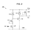
- the intermediate voltage generating circuit 150 includes an n-channel enhancement transistor 127 receiving the control signal 107 at its control terminal (gate), n-channel depletion transistors 117 and 128 serving as constant current devices, a p-channel enhancement transistor 118, and two zener diodes 116 and 119, and is coupled between the first power supply line 101a and the third power supply line 126a as illustrated in FIG. 2 .
- an intermediate voltage which will be described later appears in an intermediate voltage line 112.
- the control signal 107 is further supplied to a complementary metal-oxide semiconductor (CMOS) inverter 113.
- CMOS complementary metal-oxide semiconductor
- the inverter 113 is operated with the first power supply line 101a and the intermediate voltage line 112 as an operating power supply.
- An output of the inverter 113 is supplied to a control terminal (gate) of a p-channel enhancement transistor 111.
- An n-channel depletion transistor 110 is coupled as a constant current device between the transistor 111 and the output terminal 103.
- a control terminal (gate) of the depletion transistor 108 serving as the shutdown transistor is coupled to a node between the transistor 110 and the transistor 111.
- the inverter 113, the transistor 110, and the transistor 111 forma control circuit which controls a voltage applied between the gate and the source of the depletion transistor 108 serving as the shutdown transistor.
- a control range thereof is, which will be apparent from the following description, a voltage smaller than a potential difference between the first power supply line 101a and the second power supply line 105a in both cases where the output transistor 102 is caused to be in the conductive state and to be in the nonconductive state.
- the voltage applied between the gate and the source of the depletion transistor 108 is limited so as to be slightly a half of a battery voltage (for example, 12 V) at the maximum.
- the semiconductor output circuit 100 there are a conductive mode in which the output transistor 102 is in the conductive state to supply power to the load 104, and a nonconductive mode in which the output transistor 102 is in the nonconductive state.
- the operation of the semiconductor output circuit 100 will be described separately according to those two modes.
- the gate drive circuit 106 is driven so as to cause the output transistor 102 to be in the conductive state, and in order to cause the output transistor 102 to be in the conductive state by a lower channel resistance, is driven so as to increase a potential of an output node of the gate drive circuit 106 to a potential at which a potential of the first power supply line 101a is boosted.
- the control signal 107 at the high level is inverted by the inverter 113, but the inverter 113 uses the first power supply line 101a and the intermediate voltage line 112 as the operating power supply.
- an output of the inverter 113 becomes a potential of the intermediate voltage line 112, and the potential is supplied to a control terminal (gate) of the transistor 111.
- the transistor 127 is caused to be in the conductive state by the control signal 107 at the high level, and a control terminal (gate) of the transistor 118 is biased with a potential obtained by subtracting a value of a voltage drop (for example, 6 V) of the zener diode 116 from the potential of the first power supply line 101a.
- the transistor 118 is operated as the source follower, and hence, assuming that a threshold voltage of the transistor 118 is Vtp, a potential of "(a potential of the first power supply line 101a). - 6 V + Vtp" is output to the intermediate voltage line 112.
- the zener diode 119 is operated as a protection device for preventing the voltage difference applied between the potential of the first power supply line 101a and the potential of the intermediate voltage line 112 from being larger than 6 V.
- a potential of the output terminal 103 is substantially equal to a ground potential, which is lower than a potential of the intermediate voltage line 112. Therefore, a node between the transistor 111 and the transistor 110 side functions as the drain of the transistor 111, and an intermediate voltage line 112 side thereof functions as the source. On this occasion, the gate of the transistor 111 is biased with the potential of the intermediate voltage line 112 as described above, with the result that the transistor 111 is caused to be in the nonconductive state.
- a gate potential of the depletion transistor 108 becomes a potential of the output terminal 103 by the depletion transistor 110.
- a source potential of the depletion transistor 108 is also the potential of the output terminal 103, with the result that the depletion transistor 108 is in the conductive state.
- the depletion transistor 108 shows a constant current characteristic, and a driving ability of the gate drive circuit 106 is sufficiently larger, whereby the gate potential of the output transistor 102 is increased to be brought into the conductive state. Accordingly, power supply to the load 104 is started.
- the conductive state of the depletion transistor 108 continues until the potential of the output terminal 103 is increased approximately to a value of "(the potential of the intermediate voltage line 112) + (a threshold voltage of the transistor 111) + 2 V".
- the transistor 111 When the potential of the output terminal 103 is larger than the above-mentioned potential, the transistor 111 is operated as the source follower, and the gate of the depletion transistor 108 is supplied with a potential of "(the potential of the intermediate voltage line 112 (potential output from the inverter 113 on this occasion)) + (the threshold voltage of the transistor 111)".
- the gate potential of the depletion transistor 108 becomes sufficiently lower than the source potential thereof (that is, potential of the output terminal 103), with the result that the depletion transistor 108 is cut off to be in the nonconductive state.
- the charge supplied from the gate drive circuit 106 is all accumulated in the gate of the output transistor 102, and hence the gate potential of the output transistor 102 becomes sufficiently higher compared with that of the first power supply line 101a, and the output transistor 102 is brought into a triode region to have a smaller resistance. Accordingly, the potential of the output terminal 103 is substantially equal to the potential of the first power supply line 101a.
- the control signal 107 becomes a low level in the nonconductive mode.
- the gate drive circuit 106 starts discharging a gate charge of the output transistor 102.
- an output of the gate drive circuit 106 may be in a high impedance state.
- the transistor 127 enters the nonconductive state by the control signal 107 at the low level, and a gate potential of the transistor 118 is made substantially equal to the potential of the first power supply line 101a.
- the transistor 118 also enters the nonconductive state, and the potential of the intermediate voltage line 112 is substantially pulled up to the potential of the first power supply line 101a by the depletion transistor 128 serving as the constant current device.
- the control signal 107 at the low level is also supplied to the inverter 113, and as described above, the potential of the intermediate voltage line 112 on this occasion is substantially equal to the potential of the first power supply line 101a, with the result that the potential substantially equal to that of the first power supply line 101a is output as an output signal of the inverter 113.
- the gate potential and the source potential of the transistor 111 become substantially equal to the potential of the first power supply line 101a, and hence the transistor 111 enters the nonconductive state. Accordingly, the gate potential of the depletion transistor 108 becomes substantially equal to the potential of the output terminal 103 by the depletion transistor 110.
- the gate potential and the source potential of the depletion transistor 108 are substantially equal to each other, and the depletion transistor 108 enters the conductive state, whereby the gate charge of the output transistor 102 is discharged to the output terminal 103.
- the voltage applied between the gate and the source of the depletion transistor 108 is equal to a potential difference between a potential of the intermediate voltage line 112 and a potential of the output terminal 103.
- the maximum value of the voltage applied between the gate and the source of the depletion transistor 108 on this occasion is a value of "(the potential of the first power supply line 101a) - 6 V + (the threshold voltage Vtp of the transistor 118) + (the threshold voltage of the transistor 111)".
- the voltage applied between the gate and the source of the depletion transistor 108 is nearly zero because of the depletion transistor 110 when the transistor 111 is in the nonconductive state, and is a value of voltage drop (2 V, for example) occurring in the depletion transistor 110 when the transistor 111 is in the conductive state.
- the gate potential and the source potential of the depletion transistor 108 are substantially equal to each other.
- the voltage applied between the gate and the source of the depletion transistor 108 is within a range of voltage difference smaller than a battery voltage (voltage difference applied between the first power supply line 101a and the second power supply line 105a) by the intermediate voltage generating circuit 150 and the control circuit including the inverter 113 and the transistors 110 and 111.
- a device having a lower breakdown voltage can be used as the depletion transistor 108, which contributes to a reduction in chip area in the case where the device is constructed into an integrated circuit.
- FIG. 3 illustrates a semiconductor output circuit 200 according to a second embodiment of the present invention.
- the same components as those of FIG. 1 are denoted by the same reference symbols, and their descriptions will be omitted.
- a control terminal (gate) and a substrate terminal (back gate) of the depletion transistor 108 are commonly connected, and further, an n-channel depletion transistor 109 serving as the constant current source is provided between the depletion transistor 108 and the output terminal 103.
- the constant current source (depletion transistor 109) may be coupled between the gate of the output transistor 102 and the depletion transistor 108.
- Adepletion transistor enters the nonconductive state when the voltage applied between the gate and the source thereof reaches a so-called cut-off voltage, and an effective cut-off voltage thereof varies depending on a shape, size, or the like of the device.
- a potential of the substrate terminal (back gate) is also controlled as in the case of the gate potential, which makes turn-off of the depletion transistor 108 more reliable.
- the load 104 contains an inductance component or requires driving of a lamp or the like at larger current in some cases, and hence the output transistor 102 is desirably turned off relatively gradually for suppressing occurrence of noise.
- the depletion transistor 109 as the constant current source when the depletion transistor 109 as the constant current source is provided, the gate charge of the output transistor 102 can be discharged at the constant current, with the result that noise generated upon turn-off of the output transistor 102 can be suppressed.
- the gate charge of the output transistor 102 is desirably discharged predominantly by the depletion transistors 108 and 109. Therefore, it is desirable that an output of the gate drive circuit 106 be in the high impedance state in response to the low level of the control signal 107.
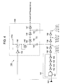
- FIG. 4 illustrates the gate drive circuit 106 for realizing the above.
- the gate drive circuit 106 of FIG. 4 includes a charge pump circuit 140, an oscillation circuit 141, and inverters 156 to 159 which supply the charge pump circuit 140 with an oscillation signal sent from the oscillation circuit 141 at an appropriate phase.
- the oscillation circuit 141 includes a NAND gate 151 and four inverters 152 to 155, and is coupled as illustrated in FIG. 4 .
- the charge pump circuit 140 includes an inverter 160, a p-channel transistor 142, an n-channel depletion transistor 143, three diodes 145 to 147, and three capacitors 148 to 150, and is coupled as illustrated in FIG. 4 .
- the oscillation circuit 141 starts an oscillation operation, and the charge pump circuit 140 is operated, whereby the gate of the output transistor 102 is supplied with a potential approximately three times the potential of the first power supply line 101a.
- the gate of the output transistor 102 is supplied with a potential approximately twice the potential of the first power supply line 101a.
- the gate charge of the output transistor 102 is discharged exclusively by the depletion transistors 108 and 109, and a discharging rate (voltage waveform) of the output transistor 102 can be determined by the depletion transistor 109 serving as the constant current source.
- FIG. 5 illustrates a semiconductor output circuit 300 according to a third embodiment of the present invention.
- the same components as those of FIG. 2 are denoted by the same reference symbols.
- a p-channel enhancement transistor 114 and a zener diode 115 which are coupled in series between the first power supply line 101a and the output terminal 103.
- a control terminal (gate) of the transistor 114 is coupled to the output node of the inverter 113, and a node between the transistor 114 and the zener diode 115 is coupled to a node between the depletion transistors 108 and 109.
- a zener voltage of the zener diode 115 is about 6 V.
- the transistor 114 In the conductive mode, the transistor 114 is in the conductive state, and the source potential of the depletion transistor 108 is substantially equal to a potential based on a zener voltage of the zener diode 115, namely the potential higher than the potential of the output terminal 103 by about 6 V.
- the gate potential of the depletion transistor 108 At a turn-on early stage of the output transistor 102 (that is, when the potential of the output terminal 103 is lower level and the transistor 111 is in the nonconductive state), the gate potential of the depletion transistor 108 is approximately equal to the potential of the output terminal 103, and the source potential of the depletion transistor 108 is approximately equal to the potential of the output terminal 103 due to the depletion transistor 109, whereby the depletion transistor 108 enters the nonconductive state.
- the depletion transistor 108 can be caused to be in the nonconductive state by the transistor 114 and the zener diode 115. Accordingly, even when the gate drive circuit 106 does not have a sufficient driving ability, the gate of the output transistor 102 can be supplied with a sufficient charge, and the potential of the output terminal 103 continues increasing.
- the source potential of the depletion transistor 108 becomes substantially equal to the potential of the first power supply line 101a.
- the gate potential and the substrate terminal (back gate) potential of the depletion transistor 108 is substantially equal to the potential related to the intermediate voltage line 112 at this stage, that is, a value of " (the potential of the first power supply line 101a) - 6 V + (the threshold voltage Vtp of the transistor 118) + (the threshold voltage of the transistor 111)".
- the voltage between the gate and the source of the depletion transistor 108 is a value of "6 V - (the threshold voltage Vtp of the transistor 118) - (the threshold voltage of the transistor 111)". Moreover, the depletion transistor 108 remains in the nonconductive state.
- the zener diode 115 functions also as the protective device between the substrate terminal (back gate) and the source.
- the transistor 114 is in the nonconductive state.
- the semiconductor output circuit 300 is operated as in the semiconductor output circuit 200, and the stand-by current does not flow.
- the depletion transistor can be used as the shutdown transistor, and the voltage range applied between the gate and the source for controlling the conductive/nonconductive state thereof can be limited, whereby the device having a relatively lower breakdown voltage can be used as the shutdown transistor. In addition, an occurrence of the stand-by current can be prevented.
Landscapes
- Electronic Switches (AREA)
- Logic Circuits (AREA)
- Metal-Oxide And Bipolar Metal-Oxide Semiconductor Integrated Circuits (AREA)
- Amplifiers (AREA)
Abstract
Description
- The present invention relates to a semiconductor output circuit, and more particularly, to a semiconductor output circuit which controls power supply to a load.
- As a semiconductor output circuit using a source follower output transistor for supplying power to a load, for example, there is a circuit disclosed in Japanese Unexamined Patent Application Publication No.
Hei 03-248619 2646786 (B2 - However, with the structure as described above, because the shutdown transistor is an enhancement type, a resistor for conductive bias is required between the gate and the source thereof, and a DC current (standby current) flows through the resistor even after the output transistor enters the nonconductive state.
- As a semiconductor output circuit of another structure, there is a circuit disclosed in Japanese Unexamined Patent Application Publication No.
Hei 06-188710 5,352,932 - A current flows through the depletion transistor even when its gate and source are at the same potential, and thus the standby current can be limited because the resistor which is required in Kanamori becomes unnecessary, which is more favorable.
- However, the inventor has noticed the following problem. In Tihanyi, in the case where the depletion transistor serving as the shutdown transistor is caused to be in a conductive state, a power supply potential is supplied to its gate, and in the case where the depletion transistor is caused to be in a nonconductive state, a ground potential is supplied to its gate. This means that, as a result, the power supply voltage is applied between the gate and the source of the depletion transistor. Accordingly, in the case where the depletion transistor is used as the shutdown transistor, it is required to use a transistor having a higher breakdown voltage, namely, a transistor having a relatively larger device area. Therefore, the inventor has sought a semiconductor output circuit not using a device having a higher breakdown voltage but using a device having a lower breakdown voltage.
- A semiconductor output circuit according to an embodiment of the present invention includes: an output transistor of a source follower configuration coupled between a first power supply line and an output terminal to be coupled to a second power supply line through a load; and a depletion transistor coupled between a control terminal of the output transistor and the output terminal. A voltage applied between a gate and a source of the depletion transistor is smaller than a voltage difference between a potential of the first power supply line and a potential of the second power supply line when the output transistor is in a conductive state and a nonconductive state.
- As a result, the voltage applied between a gate and a source for controlling the conductive state/nonconductive state of the depletion transistor is controlled not at a battery voltage level, but within a voltage range smaller than the battery voltage level, whereby a device having a relatively lower breakdown voltage can be used as the depletion transistor provided as a shutdown transistor.
- As a control voltage for the depletion transistor, an intermediate voltage between the potential of the first power supply line and the potential of the second power supply line is preferably generated. In a case where the output transistor is in the conductive state, the gate of the depletion transistor is preferably applied a potential related to the intermediate voltage, while in a case where the output transistor is caused to be in the nonconductive state, an electrical short circuit is preferably caused between the gate and the source of the depletion transistor.
- The above and other objects, advantages and features of the present invention will be more apparent from the following description of certain preferred embodiments taken in conjunction with the accompanying drawings, in which:
-
FIG. 1 is a circuit diagram of asemiconductor output circuit 100 according to a first embodiment of the present invention; -
FIG. 2 is a circuit diagram illustrating an intermediate voltage generatingcircuit 150 ofFIG. 1 ; -
FIG. 3 is a circuit diagram of asemiconductor output circuit 200 according to a second embodiment of the present invention; -
FIG. 4 is a circuit diagram illustrating agate drive circuit 106 ofFIG. 3 ; and -
FIG. 5 is a circuit diagram of asemiconductor output circuit 300 according to a third embodiment of the present invention. - The invention will now be described herein with reference to illustrative embodiments. Those skilled in the art will recognize that many alternative embodiments can be accomplished using the teachings of the present invention and that the invention is not limited to the embodiments illustrated for explanatory purposes.
- Hereinafter, embodiments of the present invention will be described in detail with reference to the drawings.
-
FIG. 1 illustrates asemiconductor output circuit 100 according to a first embodiment of the present invention, which is particularly a semiconductor output circuit excellent in application to automotive electrical components. A positive terminal of a battery is coupled to a firstpower supply terminal 101, and a negative terminal of the battery is coupled to a secondpower supply terminal 105, whereby a battery voltage (12 V , for example) as a power supply voltage is supplied. A firstpower supply line 101a and a secondpower supply line 105a are coupled to the firstpower supply terminal 101 and the secondpower supply terminal 105, respectively. A drain and a source of an n-channelenhancement output transistor 102 are coupled to the firstpower supply line 101a and anoutput terminal 103, respectively so that the n-channelenhancement output transistor 102 serves as a source follower. Aload 104 is coupled between theoutput terminal 103 and the secondpower supply line 105a. - An n-
channel depletion transistor 108 is coupled as a shutdown transistor between a control terminal (gate) of theoutput transistor 102 and theoutput terminal 103. - A control (gate) potential is supplied to the control terminal (gate) of the
output transistor 102 by agate drive circuit 106 based on acontrol signal 107 which controls a conductive state/nonconductive state of theoutput transistor 102. Thegate drive circuit 106 is operated in response to a voltage supplied between the firstpower supply line 101a and a thirdpower supply line 126a. The thirdpower supply line 126a is coupled to the negative terminal of the battery through a thirdpower supply terminal 126. Thus thegate drive circuit 106 is operated at nearly a battery voltage. Incidentally, the secondpower supply terminal 105 and the thirdpower supply terminal 126 are frequently connected to different nodes in an automotive electrical system apart from each other. Thereby voltage deference of about 2 V may occur between the secondpower supply line 105a and the thirdpower supply line 126a. - The voltage applied between the first
power supply line 101a and the thirdpower supply line 126a is further supplied to an intermediatevoltage generating circuit 150. As illustrated inFIG. 2 , the intermediatevoltage generating circuit 150 includes an n-channel enhancement transistor 127 receiving thecontrol signal 107 at its control terminal (gate), n-channel depletion transistors channel enhancement transistor 118, and twozener diodes power supply line 101a and the thirdpower supply line 126a as illustrated inFIG. 2 . As a result, an intermediate voltage which will be described later appears in anintermediate voltage line 112. - The
control signal 107 is further supplied to a complementary metal-oxide semiconductor (CMOS)inverter 113. Theinverter 113 is operated with the firstpower supply line 101a and theintermediate voltage line 112 as an operating power supply. An output of theinverter 113 is supplied to a control terminal (gate) of a p-channel enhancement transistor 111. An n-channel depletion transistor 110 is coupled as a constant current device between thetransistor 111 and theoutput terminal 103. - A control terminal (gate) of the
depletion transistor 108 serving as the shutdown transistor is coupled to a node between thetransistor 110 and thetransistor 111. - In this manner, the
inverter 113, thetransistor 110, and thetransistor 111 forma control circuit which controls a voltage applied between the gate and the source of thedepletion transistor 108 serving as the shutdown transistor. A control range thereof is, which will be apparent from the following description, a voltage smaller than a potential difference between the firstpower supply line 101a and the secondpower supply line 105a in both cases where theoutput transistor 102 is caused to be in the conductive state and to be in the nonconductive state. For example, the voltage applied between the gate and the source of thedepletion transistor 108 is limited so as to be slightly a half of a battery voltage (for example, 12 V) at the maximum. - Next, an operation of the
semiconductor output circuit 100 will be described in detail. Here, in thesemiconductor output circuit 100, there are a conductive mode in which theoutput transistor 102 is in the conductive state to supply power to theload 104, and a nonconductive mode in which theoutput transistor 102 is in the nonconductive state. The operation of thesemiconductor output circuit 100 will be described separately according to those two modes. - First, in the conductive mode, when the
control signal 107 is at a high level, thegate drive circuit 106 is driven so as to cause theoutput transistor 102 to be in the conductive state, and in order to cause theoutput transistor 102 to be in the conductive state by a lower channel resistance, is driven so as to increase a potential of an output node of thegate drive circuit 106 to a potential at which a potential of the firstpower supply line 101a is boosted. - The
control signal 107 at the high level is inverted by theinverter 113, but theinverter 113 uses the firstpower supply line 101a and theintermediate voltage line 112 as the operating power supply. Thus, an output of theinverter 113 becomes a potential of theintermediate voltage line 112, and the potential is supplied to a control terminal (gate) of thetransistor 111. - On this occasion, in the intermediate voltage generating circuit 150 (of
FIG. 2 ), thetransistor 127 is caused to be in the conductive state by thecontrol signal 107 at the high level, and a control terminal (gate) of thetransistor 118 is biased with a potential obtained by subtracting a value of a voltage drop (for example, 6 V) of thezener diode 116 from the potential of the firstpower supply line 101a. Thetransistor 118 is operated as the source follower, and hence, assuming that a threshold voltage of thetransistor 118 is Vtp, a potential of "(a potential of the firstpower supply line 101a). - 6 V + Vtp" is output to theintermediate voltage line 112. It should be noted that thezener diode 119 is operated as a protection device for preventing the voltage difference applied between the potential of the firstpower supply line 101a and the potential of theintermediate voltage line 112 from being larger than 6 V. - At an early stage of a turn-on of the
output transistor 102, a potential of theoutput terminal 103 is substantially equal to a ground potential, which is lower than a potential of theintermediate voltage line 112. Therefore, a node between thetransistor 111 and thetransistor 110 side functions as the drain of thetransistor 111, and anintermediate voltage line 112 side thereof functions as the source. On this occasion, the gate of thetransistor 111 is biased with the potential of theintermediate voltage line 112 as described above, with the result that thetransistor 111 is caused to be in the nonconductive state. - As a result, a gate potential of the
depletion transistor 108 becomes a potential of theoutput terminal 103 by thedepletion transistor 110. A source potential of thedepletion transistor 108 is also the potential of theoutput terminal 103, with the result that thedepletion transistor 108 is in the conductive state. - Thus, a part of the output from the
gate drive circuit 106 flows into theoutput terminal 103 through thedepletion transistor 108. However, in this case, thedepletion transistor 108 shows a constant current characteristic, and a driving ability of thegate drive circuit 106 is sufficiently larger, whereby the gate potential of theoutput transistor 102 is increased to be brought into the conductive state. Accordingly, power supply to theload 104 is started. - The conductive state of the
depletion transistor 108 continues until the potential of theoutput terminal 103 is increased approximately to a value of "(the potential of the intermediate voltage line 112) + (a threshold voltage of the transistor 111) + 2 V". - When the potential of the
output terminal 103 is larger than the above-mentioned potential, thetransistor 111 is operated as the source follower, and the gate of thedepletion transistor 108 is supplied with a potential of "(the potential of the intermediate voltage line 112 (potential output from theinverter 113 on this occasion)) + (the threshold voltage of the transistor 111)". As a result, the gate potential of thedepletion transistor 108 becomes sufficiently lower than the source potential thereof (that is, potential of the output terminal 103), with the result that thedepletion transistor 108 is cut off to be in the nonconductive state. - As a result, the charge supplied from the
gate drive circuit 106 is all accumulated in the gate of theoutput transistor 102, and hence the gate potential of theoutput transistor 102 becomes sufficiently higher compared with that of the firstpower supply line 101a, and theoutput transistor 102 is brought into a triode region to have a smaller resistance. Accordingly, the potential of theoutput terminal 103 is substantially equal to the potential of the firstpower supply line 101a. - Then, the
control signal 107 becomes a low level in the nonconductive mode. As a result, thegate drive circuit 106 starts discharging a gate charge of theoutput transistor 102. Instead of discharging, an output of thegate drive circuit 106 may be in a high impedance state. - On the other hand, in the intermediate voltage generating circuit 150 (of
FIG. 2 ), thetransistor 127 enters the nonconductive state by thecontrol signal 107 at the low level, and a gate potential of thetransistor 118 is made substantially equal to the potential of the firstpower supply line 101a. Thetransistor 118 also enters the nonconductive state, and the potential of theintermediate voltage line 112 is substantially pulled up to the potential of the firstpower supply line 101a by thedepletion transistor 128 serving as the constant current device. - The
control signal 107 at the low level is also supplied to theinverter 113, and as described above, the potential of theintermediate voltage line 112 on this occasion is substantially equal to the potential of the firstpower supply line 101a, with the result that the potential substantially equal to that of the firstpower supply line 101a is output as an output signal of theinverter 113. - In this manner, the gate potential and the source potential of the
transistor 111 become substantially equal to the potential of the firstpower supply line 101a, and hence thetransistor 111 enters the nonconductive state. Accordingly, the gate potential of thedepletion transistor 108 becomes substantially equal to the potential of theoutput terminal 103 by thedepletion transistor 110. - The gate potential and the source potential of the
depletion transistor 108 are substantially equal to each other, and thedepletion transistor 108 enters the conductive state, whereby the gate charge of theoutput transistor 102 is discharged to theoutput terminal 103. - Even when the gate charge of the
output transistor 102 is completely discharged, the gate of theoutput transistor 102 and theoutput terminal 103 are caused to be in a short-circuited state by thedepletion transistor 108, whereby the nonconductive state of theoutput transistor 102 is maintained even when the potential fluctuation occurs in theoutput terminal 103. Moreover, on this occasion, there is no path through which current flows from the firstpower supply line 101a to theoutput terminal 103, and thus the stand-by current does not flow. Further, there is also no path in the intermediatevoltage generating circuit 150 and a control circuit including theinverter 113 andtransistors output transistor 102, through which the stand-by current flows. - As described above, in the
semiconductor output circuit 100, during a period when theoutput transistor 102 is shifted from the nonconductive state to the conductive state and a period when theoutput transistor 102 is maintained in the conductive state, the voltage applied between the gate and the source of thedepletion transistor 108 is equal to a potential difference between a potential of theintermediate voltage line 112 and a potential of theoutput terminal 103. The maximum value of the voltage applied between the gate and the source of thedepletion transistor 108 on this occasion is a value of "(the potential of the firstpower supply line 101a) - 6 V + (the threshold voltage Vtp of the transistor 118) + (the threshold voltage of the transistor 111)". According to the operation described above, the voltage applied between the gate and the source of thedepletion transistor 108 is nearly zero because of thedepletion transistor 110 when thetransistor 111 is in the nonconductive state, and is a value of voltage drop (2 V, for example) occurring in thedepletion transistor 110 when thetransistor 111 is in the conductive state. - On the other hand, during periods when the
output transistor 102 is shifted from the conductive state to the nonconductive state and ismaintained in the nonconductive state, the gate potential and the source potential of thedepletion transistor 108 are substantially equal to each other. In other words, even in the cases where thedepletion transistor 108 is in the conductive state and is in the nonconductive state, the voltage applied between the gate and the source of thedepletion transistor 108 is within a range of voltage difference smaller than a battery voltage (voltage difference applied between the firstpower supply line 101a and the secondpower supply line 105a) by the intermediatevoltage generating circuit 150 and the control circuit including theinverter 113 and thetransistors depletion transistor 108, which contributes to a reduction in chip area in the case where the device is constructed into an integrated circuit. - It should be noted that, in the description above, it is possible to appropriately substitute a resistor for the constant current device. In other words, a so-called impedance device can be used. Moreover, the number of constant current devices, the number of zener diodes, and a zener voltage thereof, which are required in accordance with a circuit constant, can be appropriately changed.
-
FIG. 3 illustrates asemiconductor output circuit 200 according to a second embodiment of the present invention. The same components as those ofFIG. 1 are denoted by the same reference symbols, and their descriptions will be omitted. - In the
semiconductor output circuit 200, a control terminal (gate) and a substrate terminal (back gate) of thedepletion transistor 108 are commonly connected, and further, an n-channel depletion transistor 109 serving as the constant current source is provided between thedepletion transistor 108 and theoutput terminal 103. The constant current source (depletion transistor 109) may be coupled between the gate of theoutput transistor 102 and thedepletion transistor 108. - Adepletion transistor enters the nonconductive state when the voltage applied between the gate and the source thereof reaches a so-called cut-off voltage, and an effective cut-off voltage thereof varies depending on a shape, size, or the like of the device. Thus, in the
semiconductor output circuit 200, a potential of the substrate terminal (back gate) is also controlled as in the case of the gate potential, which makes turn-off of thedepletion transistor 108 more reliable. - Further, in application to automotive electrical components, the
load 104 contains an inductance component or requires driving of a lamp or the like at larger current in some cases, and hence theoutput transistor 102 is desirably turned off relatively gradually for suppressing occurrence of noise. - Therefore, when the
depletion transistor 109 as the constant current source is provided, the gate charge of theoutput transistor 102 can be discharged at the constant current, with the result that noise generated upon turn-off of theoutput transistor 102 can be suppressed. - In order to reliably discharge the gate charge at the constant current, the gate charge of the
output transistor 102 is desirably discharged predominantly by thedepletion transistors gate drive circuit 106 be in the high impedance state in response to the low level of thecontrol signal 107. -
FIG. 4 illustrates thegate drive circuit 106 for realizing the above. Thegate drive circuit 106 ofFIG. 4 includes acharge pump circuit 140, anoscillation circuit 141, andinverters 156 to 159 which supply thecharge pump circuit 140 with an oscillation signal sent from theoscillation circuit 141 at an appropriate phase. - The
oscillation circuit 141 includes aNAND gate 151 and four inverters 152 to 155, and is coupled as illustrated inFIG. 4 . Thecharge pump circuit 140 includes aninverter 160, a p-channel transistor 142, an n-channel depletion transistor 143, threediodes 145 to 147, and threecapacitors 148 to 150, and is coupled as illustrated inFIG. 4 . - When the
control signal 107 is at a high level, theoscillation circuit 141 starts an oscillation operation, and thecharge pump circuit 140 is operated, whereby the gate of theoutput transistor 102 is supplied with a potential approximately three times the potential of the firstpower supply line 101a. In the case where theinverter 159, thecapacitor 150, and thediode 147 are omitted, the gate of theoutput transistor 102 is supplied with a potential approximately twice the potential of the firstpower supply line 101a. - When the
control signal 107 becomes a low level, the oscillation operation of theoscillation circuit 141 is stopped. Besides, thetransistor 142 enters the nonconductive state, and accordingly, a cathode of thediode 147, namely, an output node of thegate drive circuit 106 enters the high impedance state. - In this manner, the gate charge of the
output transistor 102 is discharged exclusively by thedepletion transistors output transistor 102 can be determined by thedepletion transistor 109 serving as the constant current source. -
FIG. 5 illustrates asemiconductor output circuit 300 according to a third embodiment of the present invention. The same components as those ofFIG. 2 are denoted by the same reference symbols. - In the
semiconductor output circuit 300, in addition to the configuration ofFIG. 2 , there are further provided a p-channel enhancement transistor 114 and azener diode 115 which are coupled in series between the firstpower supply line 101a and theoutput terminal 103. A control terminal (gate) of thetransistor 114 is coupled to the output node of theinverter 113, and a node between thetransistor 114 and thezener diode 115 is coupled to a node between thedepletion transistors zener diode 115 is about 6 V. - In the conductive mode, the
transistor 114 is in the conductive state, and the source potential of thedepletion transistor 108 is substantially equal to a potential based on a zener voltage of thezener diode 115, namely the potential higher than the potential of theoutput terminal 103 by about 6 V. At a turn-on early stage of the output transistor 102 (that is, when the potential of theoutput terminal 103 is lower level and thetransistor 111 is in the nonconductive state), the gate potential of thedepletion transistor 108 is approximately equal to the potential of theoutput terminal 103, and the source potential of thedepletion transistor 108 is approximately equal to the potential of theoutput terminal 103 due to thedepletion transistor 109, whereby thedepletion transistor 108 enters the nonconductive state. In other words, at the turn-on early stage of theoutput transistor 102, thedepletion transistor 108 can be caused to be in the nonconductive state by thetransistor 114 and thezener diode 115. Accordingly, even when thegate drive circuit 106 does not have a sufficient driving ability, the gate of theoutput transistor 102 can be supplied with a sufficient charge, and the potential of theoutput terminal 103 continues increasing. - After that, when the potential of the
output terminal 103 is increased and becomes higher than the zener voltage of thezener diode 115, the source potential of thedepletion transistor 108 becomes substantially equal to the potential of the firstpower supply line 101a. On this occasion, because thetransistor 111 is in the conductive state, the gate potential and the substrate terminal (back gate) potential of thedepletion transistor 108 is substantially equal to the potential related to theintermediate voltage line 112 at this stage, that is, a value of " (the potential of the firstpower supply line 101a) - 6 V + (the threshold voltage Vtp of the transistor 118) + (the threshold voltage of the transistor 111)". In other words, the voltage between the gate and the source of thedepletion transistor 108 is a value of "6 V - (the threshold voltage Vtp of the transistor 118) - (the threshold voltage of the transistor 111)". Moreover, thedepletion transistor 108 remains in the nonconductive state. - Further, when an n-channel metal-oxide semiconductor field-effect transistor (MOSFET) having a lower breakdown voltage structure is used for the
depletion transistor 108, thezener diode 115 functions also as the protective device between the substrate terminal (back gate) and the source. - On the other hand, in the nonconductive mode of the
output transistor 102, thetransistor 114 is in the nonconductive state. Thus, thesemiconductor output circuit 300 is operated as in thesemiconductor output circuit 200, and the stand-by current does not flow. - As described above, the depletion transistor can be used as the shutdown transistor, and the voltage range applied between the gate and the source for controlling the conductive/nonconductive state thereof can be limited, whereby the device having a relatively lower breakdown voltage can be used as the shutdown transistor. In addition, an occurrence of the stand-by current can be prevented.
- Although the invention has been described above in connection with several preferred embodiments thereof, it will be appreciated by those skilled in the art that those embodiments are provided solely for illustrating the invention, and should not be relied upon to construe the appended claims in a limiting sense.
Claims (9)
- A semiconductor output circuit, comprising:a first power supply line;an output terminal to be coupled to a second power supply line through a load;an output transistor coupled between the first power supply line and the output terminal; anda depletion transistor coupled between a control terminal of the output transistor and the output terminal,wherein a voltage applied between a gate and a source of the depletion transistor is smaller than a voltage difference between a potential of the first power supply line and a potential of the second power supply line when the output transistor is in a conductive state and a nonconductive state.
- A semiconductor output circuit according to claim 1, further comprising:an intermediate voltage generating circuit generating an intermediate potential between the potential of the first power supply line and the potential of the second power supply line to a intermediate voltage line; anda control circuit which causes the gate of the depletion transistor to have a potential related to the intermediate voltage in a case of causing the output transistor to be in the conductive state, and couples the gate and the source of the depletion transistor in a case of causing the output transistor to be in the nonconductive state.
- A semiconductor output circuit according to claim 2, wherein:the output transistor is driven in response to a control signal; andthe control circuit comprises:a series circuit of a switch transistor and an impedance device, which are coupled between the intermediate voltage line and the output terminal; andan inverter which is operated at a voltage between the potential of the first power supply line and the inter mediate potential of the intermediate voltage line, and inverts the control signal to supply the inverted control signal to a gate of the switch transistor.
- A semiconductor output circuit according to claim 3, wherein the switch transistor of the control circuit is defined as a first switch transistor, the control circuit further comprising:a series circuit of a second switch transistor and a constant voltage device, which are provided between the first power supply line and the output terminal,whereinan output of the inverter is supplied to a gate of the second switch transistor, anda node between the second switch transistor and the constant voltage device is coupled to the source of the depletion transistor.
- A semiconductor output circuit according to claim 1, where in the depletion transistor has a substrate terminal coupled to the gate thereof.
- A semiconductor output circuit according to claim 1, further comprises a constant current source device provided in series with the depletion transistor between the control terminal of the output transistor and the output terminal.
- A semiconductor output circuit according to claim 6, wherein the constant current source device comprises a depletion transistor.
- A semiconductor output circuit according to claim 1, wherein:the output transistor is driven by a gate drive circuit; andan output of the gate drive circuit becomes a high impedance state when the output transistor is shifted from the conductive state to the nonconductive state.
- A semiconductor output circuit according to claim 8, wherein the gate drive circuit generates a potential higher than a potential of the first power supply line in response to the control signal which causes the output transistor to be in the conductive state.
Applications Claiming Priority (2)
| Application Number | Priority Date | Filing Date | Title |
|---|---|---|---|
| JP2007329472 | 2007-12-21 | ||
| JP2008294518A JP5226474B2 (en) | 2007-12-21 | 2008-11-18 | Semiconductor output circuit |
Publications (3)
| Publication Number | Publication Date |
|---|---|
| EP2073385A2 true EP2073385A2 (en) | 2009-06-24 |
| EP2073385A3 EP2073385A3 (en) | 2013-03-13 |
| EP2073385B1 EP2073385B1 (en) | 2015-03-18 |
Family
ID=40513406
Family Applications (1)
| Application Number | Title | Priority Date | Filing Date |
|---|---|---|---|
| EP08021554.4A Active EP2073385B1 (en) | 2007-12-21 | 2008-12-11 | Semiconductor output circuit for controlling power supply to a load |
Country Status (2)
| Country | Link |
|---|---|
| US (1) | US7834669B2 (en) |
| EP (1) | EP2073385B1 (en) |
Cited By (1)
| Publication number | Priority date | Publication date | Assignee | Title |
|---|---|---|---|---|
| EP3218977A4 (en) * | 2014-11-12 | 2018-06-20 | Texas Instruments Incorporated | Output discharge techniques for load switches |
Families Citing this family (6)
| Publication number | Priority date | Publication date | Assignee | Title |
|---|---|---|---|---|
| JP2010193033A (en) * | 2009-02-17 | 2010-09-02 | Renesas Electronics Corp | Overcurrent protection circuit |
| JP5341781B2 (en) * | 2010-01-04 | 2013-11-13 | ルネサスエレクトロニクス株式会社 | Power supply control circuit |
| JP5341780B2 (en) * | 2010-01-04 | 2013-11-13 | ルネサスエレクトロニクス株式会社 | Power supply control circuit |
| JP5889723B2 (en) | 2012-06-07 | 2016-03-22 | ルネサスエレクトロニクス株式会社 | Semiconductor device |
| US9917578B2 (en) | 2016-02-19 | 2018-03-13 | Infineon Technologies Austria Ag | Active gate-source capacitance clamp for normally-off HEMT |
| JP6871514B2 (en) * | 2017-06-30 | 2021-05-12 | ミツミ電機株式会社 | Negative power control circuit and power supply |
Citations (2)
| Publication number | Priority date | Publication date | Assignee | Title |
|---|---|---|---|---|
| JPH03248619A (en) | 1990-02-27 | 1991-11-06 | Nec Corp | Semiconductor output circuit |
| JPH06188710A (en) | 1992-06-05 | 1994-07-08 | Siemens Ag | Control circuit for electric power fet |
Family Cites Families (8)
| Publication number | Priority date | Publication date | Assignee | Title |
|---|---|---|---|---|
| US5055722A (en) * | 1989-12-20 | 1991-10-08 | Sundstrand Corporation | Gate drive for insulated gate device |
| EP0489935B1 (en) * | 1990-11-09 | 1995-11-02 | Siemens Aktiengesellschaft | MOSFET switch for an inductive load |
| US5272399A (en) * | 1992-02-25 | 1993-12-21 | Siemens Aktiengesellschaft | Circuit limiting the load current of a power MOSFET |
| US5910738A (en) * | 1995-04-07 | 1999-06-08 | Kabushiki Kaisha Toshiba | Driving circuit for driving a semiconductor device at high speed and method of operating the same |
| DE19631751C1 (en) * | 1996-08-06 | 1997-11-27 | Siemens Ag | Power FET control circuit for lamp switching |
| JP3248619B2 (en) | 1999-03-05 | 2002-01-21 | ティーディーケイ株式会社 | High voltage feedthrough capacitors and magnetrons |
| DE10033440C2 (en) * | 2000-07-10 | 2002-07-18 | Infineon Technologies Ag | Drive circuit for a power MOSFET |
| DE10038220C2 (en) * | 2000-08-04 | 2002-07-25 | Infineon Technologies Ag | Overcurrent-protected semiconductor circuit breaker with charge pump |
-
2008
- 2008-12-10 US US12/314,420 patent/US7834669B2/en active Active
- 2008-12-11 EP EP08021554.4A patent/EP2073385B1/en active Active
Patent Citations (4)
| Publication number | Priority date | Publication date | Assignee | Title |
|---|---|---|---|---|
| JPH03248619A (en) | 1990-02-27 | 1991-11-06 | Nec Corp | Semiconductor output circuit |
| JP2646786B2 (en) | 1990-02-27 | 1997-08-27 | 日本電気株式会社 | Semiconductor output circuit |
| JPH06188710A (en) | 1992-06-05 | 1994-07-08 | Siemens Ag | Control circuit for electric power fet |
| US5352932A (en) | 1992-06-05 | 1994-10-04 | Siemens Aktiengesellschaft | Trigger circuit for a power FET with a load on the source side |
Cited By (2)
| Publication number | Priority date | Publication date | Assignee | Title |
|---|---|---|---|---|
| EP3218977A4 (en) * | 2014-11-12 | 2018-06-20 | Texas Instruments Incorporated | Output discharge techniques for load switches |
| US10187055B2 (en) | 2014-11-12 | 2019-01-22 | Texas Instruments Incorporated | Output discharge techniques for load switches |
Also Published As
| Publication number | Publication date |
|---|---|
| EP2073385B1 (en) | 2015-03-18 |
| US7834669B2 (en) | 2010-11-16 |
| US20090160498A1 (en) | 2009-06-25 |
| EP2073385A3 (en) | 2013-03-13 |
Similar Documents
| Publication | Publication Date | Title |
|---|---|---|
| US8040162B2 (en) | Switch matrix drive circuit for a power element | |
| US8547142B2 (en) | Power semiconductor device and operation method thereof | |
| EP2315354B1 (en) | Semiconductor device | |
| CN110958003B (en) | Adaptive gate driver | |
| EP2073385B1 (en) | Semiconductor output circuit for controlling power supply to a load | |
| US20200028503A1 (en) | Semiconductor device and electronic control device | |
| JP7846661B2 (en) | Semiconductor equipment | |
| US11711010B2 (en) | Drive circuit and inverter device | |
| JP2003235244A (en) | Rush current limit and noise reduction circuit for PFM control charge pump | |
| CN112640279B (en) | Overcurrent protection circuit and switch circuit | |
| EP2073386B1 (en) | Semiconductor output circuit | |
| US7551004B2 (en) | Inverter apparatus with improved gate drive for power MOSFET | |
| US20110057633A1 (en) | Load driving circuit | |
| US6856177B1 (en) | High side power switch with charge pump and bootstrap capacitor | |
| US6844769B2 (en) | Drive circuit | |
| US20050110556A1 (en) | Bootstrap driver | |
| JP2020025158A (en) | High breakdown voltage integrated circuit | |
| US11070202B2 (en) | Signal transmission circuit, switch driving device, and power module | |
| JP5226474B2 (en) | Semiconductor output circuit | |
| TW202324933A (en) | Pre-driven bootstrapping drivers | |
| US11777497B1 (en) | Efficiency concept for driving a PMOS and NMOS full-bridge power stage | |
| JP2009171552A (en) | Semiconductor output circuit | |
| JP3824602B2 (en) | Switching control device and switching control method | |
| JP2022006505A (en) | Charge pump device |
Legal Events
| Date | Code | Title | Description |
|---|---|---|---|
| PUAI | Public reference made under article 153(3) epc to a published international application that has entered the european phase |
Free format text: ORIGINAL CODE: 0009012 |
|
| AK | Designated contracting states |
Kind code of ref document: A2 Designated state(s): AT BE BG CH CY CZ DE DK EE ES FI FR GB GR HR HU IE IS IT LI LT LU LV MC MT NL NO PL PT RO SE SI SK TR |
|
| AX | Request for extension of the european patent |
Extension state: AL BA MK RS |
|
| RAP1 | Party data changed (applicant data changed or rights of an application transferred) |
Owner name: RENESAS ELECTRONICS CORPORATION |
|
| REG | Reference to a national code |
Ref country code: DE Ref legal event code: R079 Ref document number: 602008037167 Country of ref document: DE Free format text: PREVIOUS MAIN CLASS: H03K0017080000 Ipc: H03K0017060000 |
|
| PUAL | Search report despatched |
Free format text: ORIGINAL CODE: 0009013 |
|
| AK | Designated contracting states |
Kind code of ref document: A3 Designated state(s): AT BE BG CH CY CZ DE DK EE ES FI FR GB GR HR HU IE IS IT LI LT LU LV MC MT NL NO PL PT RO SE SI SK TR |
|
| AX | Request for extension of the european patent |
Extension state: AL BA MK RS |
|
| RIC1 | Information provided on ipc code assigned before grant |
Ipc: H03K 17/06 20060101AFI20130207BHEP Ipc: H03K 17/16 20060101ALI20130207BHEP |
|
| 17P | Request for examination filed |
Effective date: 20130725 |
|
| RBV | Designated contracting states (corrected) |
Designated state(s): AT BE BG CH CY CZ DE DK EE ES FI FR GB GR HR HU IE IS IT LI LT LU LV MC MT NL NO PL PT RO SE SI SK TR |
|
| 17Q | First examination report despatched |
Effective date: 20130906 |
|
| AKX | Designation fees paid |
Designated state(s): DE |
|
| GRAP | Despatch of communication of intention to grant a patent |
Free format text: ORIGINAL CODE: EPIDOSNIGR1 |
|
| GRAJ | Information related to disapproval of communication of intention to grant by the applicant or resumption of examination proceedings by the epo deleted |
Free format text: ORIGINAL CODE: EPIDOSDIGR1 |
|
| GRAP | Despatch of communication of intention to grant a patent |
Free format text: ORIGINAL CODE: EPIDOSNIGR1 |
|
| INTG | Intention to grant announced |
Effective date: 20140924 |
|
| RAP1 | Party data changed (applicant data changed or rights of an application transferred) |
Owner name: RENESAS ELECTRONICS CORPORATION |
|
| INTG | Intention to grant announced |
Effective date: 20141007 |
|
| GRAS | Grant fee paid |
Free format text: ORIGINAL CODE: EPIDOSNIGR3 |
|
| GRAA | (expected) grant |
Free format text: ORIGINAL CODE: 0009210 |
|
| AK | Designated contracting states |
Kind code of ref document: B1 Designated state(s): DE |
|
| REG | Reference to a national code |
Ref country code: DE Ref legal event code: R096 Ref document number: 602008037167 Country of ref document: DE Effective date: 20150430 |
|
| REG | Reference to a national code |
Ref country code: DE Ref legal event code: R097 Ref document number: 602008037167 Country of ref document: DE |
|
| PLBE | No opposition filed within time limit |
Free format text: ORIGINAL CODE: 0009261 |
|
| STAA | Information on the status of an ep patent application or granted ep patent |
Free format text: STATUS: NO OPPOSITION FILED WITHIN TIME LIMIT |
|
| 26N | No opposition filed |
Effective date: 20151221 |
|
| REG | Reference to a national code |
Ref country code: DE Ref legal event code: R082 Ref document number: 602008037167 Country of ref document: DE Representative=s name: GLAWE DELFS MOLL PARTNERSCHAFT MBB VON PATENT-, DE Ref country code: DE Ref legal event code: R081 Ref document number: 602008037167 Country of ref document: DE Owner name: RENESAS ELECTRONICS CORPORATION, JP Free format text: FORMER OWNER: RENESAS ELECTRONICS CORP., KAWASAKI-SHI, KANAGAWA, JP |
|
| REG | Reference to a national code |
Ref country code: DE Ref legal event code: R082 Ref document number: 602008037167 Country of ref document: DE Representative=s name: GLAWE DELFS MOLL PARTNERSCHAFT MBB VON PATENT-, DE Ref country code: DE Ref legal event code: R082 Ref document number: 602008037167 Country of ref document: DE Representative=s name: GLAWE DELFS MOLL PARTGMBB, DE |
|
| PGFP | Annual fee paid to national office [announced via postgrant information from national office to epo] |
Ref country code: DE Payment date: 20251229 Year of fee payment: 18 |