EP2073309A1 - Dual polarised radiating element for cellular base station antennas - Google Patents
Dual polarised radiating element for cellular base station antennas Download PDFInfo
- Publication number
- EP2073309A1 EP2073309A1 EP07291582A EP07291582A EP2073309A1 EP 2073309 A1 EP2073309 A1 EP 2073309A1 EP 07291582 A EP07291582 A EP 07291582A EP 07291582 A EP07291582 A EP 07291582A EP 2073309 A1 EP2073309 A1 EP 2073309A1
- Authority
- EP
- European Patent Office
- Prior art keywords
- radiating
- dual polarised
- radiating element
- reflector surface
- flanges
- Prior art date
- Legal status (The legal status is an assumption and is not a legal conclusion. Google has not performed a legal analysis and makes no representation as to the accuracy of the status listed.)
- Granted
Links
- 230000009977 dual effect Effects 0.000 title claims abstract description 21
- 230000001413 cellular effect Effects 0.000 title claims abstract description 7
- 230000005404 monopole Effects 0.000 claims abstract description 42
- 230000005855 radiation Effects 0.000 claims abstract description 4
- 239000002184 metal Substances 0.000 description 5
- 238000004519 manufacturing process Methods 0.000 description 3
- 238000005452 bending Methods 0.000 description 2
- 238000004088 simulation Methods 0.000 description 2
- 208000004350 Strabismus Diseases 0.000 description 1
- 230000005684 electric field Effects 0.000 description 1
- 238000005516 engineering process Methods 0.000 description 1
- 230000005284 excitation Effects 0.000 description 1
- 238000005259 measurement Methods 0.000 description 1
- 230000006641 stabilisation Effects 0.000 description 1
Images

Classifications
-
- H—ELECTRICITY
- H01—ELECTRIC ELEMENTS
- H01Q—ANTENNAS, i.e. RADIO AERIALS
- H01Q9/00—Electrically-short antennas having dimensions not more than twice the operating wavelength and consisting of conductive active radiating elements
- H01Q9/04—Resonant antennas
- H01Q9/30—Resonant antennas with feed to end of elongated active element, e.g. unipole
- H01Q9/32—Vertical arrangement of element
- H01Q9/36—Vertical arrangement of element with top loading
-
- H—ELECTRICITY
- H01—ELECTRIC ELEMENTS
- H01Q—ANTENNAS, i.e. RADIO AERIALS
- H01Q1/00—Details of, or arrangements associated with, antennas
- H01Q1/12—Supports; Mounting means
- H01Q1/22—Supports; Mounting means by structural association with other equipment or articles
- H01Q1/24—Supports; Mounting means by structural association with other equipment or articles with receiving set
- H01Q1/241—Supports; Mounting means by structural association with other equipment or articles with receiving set used in mobile communications, e.g. GSM
- H01Q1/246—Supports; Mounting means by structural association with other equipment or articles with receiving set used in mobile communications, e.g. GSM specially adapted for base stations
-
- H—ELECTRICITY
- H01—ELECTRIC ELEMENTS
- H01Q—ANTENNAS, i.e. RADIO AERIALS
- H01Q21/00—Antenna arrays or systems
- H01Q21/24—Combinations of antenna units polarised in different directions for transmitting or receiving circularly and elliptically polarised waves or waves linearly polarised in any direction
-
- H—ELECTRICITY
- H01—ELECTRIC ELEMENTS
- H01Q—ANTENNAS, i.e. RADIO AERIALS
- H01Q21/00—Antenna arrays or systems
- H01Q21/30—Combinations of separate antenna units operating in different wavebands and connected to a common feeder system
Definitions
- the present invention relates to a dual polarised radiating element for a cellular base station antenna. Recently, the demand for antennas for mobile and wireless applications has increased dramatically. There are now a number of land based systems for wireless communications using a wide range of frequency bands.
- antennas having electrical dipoles located one quarter of a wavelength above a finite ground plane formed by a reflector. Dual polarisation is achieved by way of orthogonal linear polarisation obtained by excitation of the respective, mutually perpendicular electrical dipoles. These electrical dipoles arc slanted 45° in opposite directions relative to the central longitudinal axis of the reflector.
- the horizontal 3dB HPBW for Half Power Beam Width
- the cross-polarisation level for example the cross-polar discrimination at +/- 60° about 5dB
- the cross-polar discrimination at +/- 60° about 5dB is too high across passbands up to 25% (for example 806-960MHz or 1700-2200MHz).
- Document US2006/0109193 discloses an antenna improving the 3dB HPBW stabilisation. Moreover, this antenna also reduces the cross-polarisation level.
- This antenna comprises an array of dual polarized radiating elements mounted on a reflector structure for reflecting polarised radiofrequency signals.
- the reflector structure has a pyramidal or conical horn-like shape for each radiating element.
- This antenna design significantly increases the manufacturing costs, since horn-like shapes require the design of specific moulds.
- a dual polarised radiating element for a cellular base station antenna comprising:
- a pair of opposite element feeds extends above the reflector surface between two opposite footings.
- each element feed comprises a first end portion capacitively coupled to a radiating monopole and a second end portion is protruding radially from said radiating monopole.
- said first end portions of the element feeds arc capacitively coupled to respective footings.
- the first end portion of an element feed is approximately perpendicular to its second end portion.
- said powering means comprises:
- said first and second connection lines have identical impedance amplitudes.
- said flanges are comprised within a common plane surface.
- said reflector surface is plane and said flanges are parallel to the reflector surface.
- said flanges are tilted relative to said reflector surface.
- each monopole further comprises at least one wing extending from a respective flange and being tilted relative to this flange.
- said flanges have a rectangular shape.
- said footings have a rectangular shape having the same length as said flanges.
- said flanges ate provided with through holes extending tangentially relative to said aperture area.
- the radiating element further comprises sidewalls protruding from said reflector surface on the same side as the radiating monopoles, said radiating monopoles being located between said sidewalls.
- intersection between the reflector surface and the lateral sidewalls form parallel lines and wherein each pair of opposite element feeds extend according to a direction forming approximately 45° with said parallel lines.
- one pair of element feeds partly covers the other pair of element feeds.
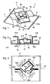
- Figures 1 and 2 illustrate a dual polarised radiating element 1 for a cellular base station antenna.
- the radiating element 1 comprises a reflector 2 for reflecting radiation energy.
- the reflector 2 of this embodiment comprises a plane portion 21 forming a reflector surface.
- a radiating portion 3 comprises four radiating electrical monopoles 4a to 4d.
- the monopoles 4a to 4d are distributed around an aperture area (illustrated by circle 8 at figure 3 ).
- Each monopole 4 comprises a footing 42 and a flange 41 formed by respective wall portions.
- Each monopole 4a to 4d can be formed out of a bended metal sheet.
- Each flange 41a to 41d is located above the plane portion 21.
- Each flange 41 is protruding from a respective footing 42 in a radial direction towards the outside. The radial direction is defined starting from the centre of the aperture area 8.
- two flanges 41 from adjacent monopoles 4 extend radially perpendicularly to each other.
- the radiating portion 3 also comprises four element feeds 5a to 5d. Each element feed 5a to 5d is capacitively coupled to a respective monopole 4a to 4d. Each element feed 5a to 5d is protruding from its respective monopole within the aperture area. An electric field is generated in the aperture area 8, forming a magnetic source. The combination of a magnetic source and of the electrical monopoles improves the 3dB HPBW stability.
- the radiating portion 3 further comprises powering means connected to the feeds 5a to 5d and for which further details are provided below.
- a radiating element according to the invention provides at least the same far field pattern performance (say horizontal 3dB HPBW stability, cross-polar discrimination, front to back ratio) across passbands up to 25% (for example 806-960MHz or 1700-2200MHz) as known radiating elements. Simulations and measurementsled on the embodiment illustrated at figures 1 and 2 provided the following results for the far field pattern:
- a radiating element according to the invention further has a simple structure whose manufacturing cost is particularly low.
- Such a radiating element 1 can be used in antennas equipping mobile phone networks.
- Each element feed 5a to 5d comprises a footing portion 52a to 52d and a flange portion 51 a to 51 d connected to the upper part of a respective footing portion.
- Each flange portion 51a to 51d is perpendicular to its respective footing portion 52a to 52d, the element feeds thus having a L-shape in cross section.
- Each flange portion 51a to 51d is thus protruding radially from a respective monopole 4a to 4d within the volume located under the aperture area 8.
- Flange portions 51a to 51d and corresponding flanges 41a to 41d are protruding in a same direction but on opposite sides.
- Each footing portion 52a to 52d is capacitively coupled to its respective radiating monopole 4a to 4d at the level of its footing 42a to 42d.
- Each pair of element feeds 5a,5c or 5b,5d extends above the plane portion 21 between two opposite footings, respectively footings 42a, 42c and 42b, 42d.
- One pair of flange portions is located higher above the plane potion 21 than the other: flange portions 51a and 51c partly cover flange portions 51b and 51d.
- the apposite flanges portions, say 51a,51c and 51b, 51d are separated by an air gap at the centre of the aperture area 8.
- Each element feed 5a to 5d can be formed out of a bended metal sheet.
- the flanges 41a to 41d have a rectangular shape.
- the footings 42a to 42d also have a rectangular shape. These flanges 41a to 41d have the same length as their respective footings 42a to 42d.
- the flanges 41a to 41d of this embodiment are parallel to the plane portion 21. These flanges 41a to 41d arc comprised within a common plane surface.
- the footings 42a to 42d are perpendicular to the plane portion 21 and to their respective flanges 41a to 41d (the monopoles 4a to 4d thus having a L-shape in cross section).
- the reflector 2 further comprises sidewalls 22 and 23.
- the sidewalls 22 and 23 may be formed simply by bending the plane surface 21.
- the monopoles 4a to 4d and the feeds 5a to 5d are located between these sidewalls 22 and 23.
- the sidewall 22 is parallel to the sidewall 23.
- the sidewalls 22 and 23 are perpendicular to the plane surface 21.
- the intersections between the sidewalls 22 and 23 and the plane surface 21 form parallel lines.
- Each pair of feeds 5 extending in a direction forming approximately a 45°angle with these parallel lines.
- Figure 3 is a top view of electrical connections made on the plane surface 21.
- powering means include a power divider, a first connection line between the power divider and the first feed, and a second connection line between the power divider and the second feed.
- the power divider 6ac comprises a three port junction connected to a connection line 7a, to another connection line 7c and to an entry line (not illustrated).
- the power divider 6bd comprises a three port junction connected to a connection line 7b, to another connection line 7d and to an entry line (not illustrated).
- connection line 7c connects the power divider 6ac to the lower end of the footing portion 52c.
- connection line 7a connects the power divider 6ac to the lower end of the footing portion 52a.
- connection line 7d connects the power divider 6bd to the lower end of the footing portion 52d.
- connection line 7b connects the power divider 6bd to the lower end of the footing portion 52b.
- connection line 7a comprises a ⁇ /2 connecting portion 7ac. This connecting portion 7ac introduces a 180° phase relative to the connection line 7c.
- the entry line will preferably have a Zin impedance amplitude equal to 50 ⁇ .
- the input power can also be unequally split using connection lines having different impedances.
- the length of the ⁇ /2 connecting portion 7ac can be shortened or lengthened to compensate for squint of the far field pattern. Connection lines may be formed using the air microstrip line technology.
- the flanges 41 a to 41 d are tilted relative to the plane portion 21 of the reflector.
- the flanges 41a to 41d also form an angle with their respective footing 42a to 42d that differs from 90°.
- the angle formed between the sidewalls 22 and 23 and the plane surface 21 is higher than 90°.
- Figure 5 is a perspective view of another possible shape for flange 41.
- the flange 41 is provided with a through hole 43.
- This hole 43 is elongated in a direction that is tangent to the aperture area 8.
- This hole 43 has a rectangular shape.
- the radiating portion 3 using such a monopole 4 provides an improved front-to-back ratio.
- FIGS 6 and 7 illustrate two alternative shapes for the monopoles 4.
- each flange 41 is fitted with at least one wing protruding therefrom in the upper direction and being tilted relative to this flange 41.
- the radiating portions 3 using such a monopole 4 provides an increased impedance bandwidth. This design helps to adapt the impedance bandwidth performance (VSWR) of the radiating element 1 to the far field pattern bandwidth
- both the flange 41 and the wing 44 have a rectangular shape with a through hole in their middle portion.
- the wing 44 is tilted relative to the surface of the flange 41.
- two wings 44 and 45 arc protruding from the flange 41.
- Wings 44 and 45 are tilted relative to the surface of the flange 41.
- the angle between both wings 44 and 45 and flange 41 arc different.
- Both the flange 41 and the wings 44 and 45 have a rectangular shape with a through hole in their muddle portion. Any other number of extending wings may be made on flange 41.
- the flange and the wings can be formed in a single metal piece by appropriate cuts and bendings.
- PIM passive intermodulation
- the illustrated radiating element 1 only comprises a radiating portion 3 but radiating elements including several aligned radiating portions can also be made according to the invention.
- the illustrated radiating monopoles 4 are independent parts but can also be made as a one-piece component.
- the illustrated flange portions 51a to 51d arc rectangular.
- other shapes can also be foreseen, notably a trapezoid shape.
Landscapes
- Engineering & Computer Science (AREA)
- Computer Networks & Wireless Communication (AREA)
- Aerials With Secondary Devices (AREA)
- Variable-Direction Aerials And Aerial Arrays (AREA)
Abstract
-a reflector surface (21) for reflecting radiation energy,
-four radiating monopoles (4a to 4d) distributed around an aperture area (9), each radiating monopole comprising a footing (42a to 42d) protruding from said reflector surface and a flange (41a to 42d) located above the reflector surface and protruding from said footing radially towards the outside, the flanges from adjacent monopoles extending radially perpendicular to each other,
wherein it further comprises:
-four element feeds (5a to 5d), each capacitively coupled to a respective monopole and protruding radially therefrom within the aperture area (8);
-powering means (6ac, 6bd, 7a to 7d, 7ac, 7bd) connected to the element feeds.
Description
- The present invention relates to a dual polarised radiating element for a cellular base station antenna. Recently, the demand for antennas for mobile and wireless applications has increased dramatically. There are now a number of land based systems for wireless communications using a wide range of frequency bands.
- Several cellular base station antenna manufacturers are proposing antennas having electrical dipoles located one quarter of a wavelength above a finite ground plane formed by a reflector. Dual polarisation is achieved by way of orthogonal linear polarisation obtained by excitation of the respective, mutually perpendicular electrical dipoles. These electrical dipoles arc slanted 45° in opposite directions relative to the central longitudinal axis of the reflector.
- Unfortunately, such antennas provide limited far field pattern performance : the horizontal 3dB HPBW (for Half Power Beam Width) stability faces large variation (for instance 65° +/-6°), the cross-polarisation level (for example the cross-polar discrimination at +/- 60° about 5dB) is too high across passbands up to 25% (for example 806-960MHz or 1700-2200MHz).
- Document
US2006/0109193 discloses an antenna improving the 3dB HPBW stabilisation. Moreover, this antenna also reduces the cross-polarisation level. This antenna comprises an array of dual polarized radiating elements mounted on a reflector structure for reflecting polarised radiofrequency signals. The reflector structure has a pyramidal or conical horn-like shape for each radiating element. - This antenna design significantly increases the manufacturing costs, since horn-like shapes require the design of specific moulds.
- In order to reduce the cross-polarisation level, other designs include lateral elongated choke reflectors fixed on both sides of a reflector. These designs lead to complex and costly manufacturing processes.
- There is thus a need for a simple antenna structure that provides good far field performance. It is therefore an object of the present invention to provide a dual polarised radiating element for a cellular base station antenna, comprising:
- a reflector surface for reflecting radiation energy,
- four radiating monopoles distributed around an aperture area, each radiating monopole comprising a footing protruding from said reflector surface and a flange located above the reflector surface and protruding from said footing radially towards the outside, the flanges from adjacent monopoles extending radially perpendicular to each other,
- four element feeds, each capacitively coupled to a respective monopole and protruding radially therefrom within the aperture area ;
- powering means connected to the element feeds.
- According to another embodiment, a pair of opposite element feeds extends above the reflector surface between two opposite footings.
- According to another embodiment, each element feed comprises a first end portion capacitively coupled to a radiating monopole and a second end portion is protruding radially from said radiating monopole.
- According to another embodiment, said first end portions of the element feeds arc capacitively coupled to respective footings.
- According to another embodiment, the first end portion of an element feed is approximately perpendicular to its second end portion.
- According to another embodiment, said powering means comprises:
- a power divider;
- a first connection line connecting the power divider to an clement feed;
- a second connection line connecting the power divider to an opposite element feed and introducing a 180° phase relative to said first connection line.
- According to another embodiment, said first and second connection lines have identical impedance amplitudes.
- According to another embodiment, said flanges are comprised within a common plane surface.
- According to another embodiment, said reflector surface is plane and said flanges are parallel to the reflector surface.
- According to another embodiment, said flanges are tilted relative to said reflector surface.
- According to another embodiment, each monopole further comprises at least one wing extending from a respective flange and being tilted relative to this flange.
- According to another embodiment, said flanges have a rectangular shape.
- According to another embodiment, said footings have a rectangular shape having the same length as said flanges.
- According to another embodiment, said flanges ate provided with through holes extending tangentially relative to said aperture area.
- According to another embodiment, the radiating element further comprises sidewalls protruding from said reflector surface on the same side as the radiating monopoles, said radiating monopoles being located between said sidewalls.
- According to another embodiment, the intersection between the reflector surface and the lateral sidewalls form parallel lines and wherein each pair of opposite element feeds extend according to a direction forming approximately 45° with said parallel lines.
- According to another embodiment, one pair of element feeds partly covers the other pair of element feeds.
- The advantage of the present invention will become apparent from the following description of several embodiments with reference to the accompanying drawings, in which :
-
Figure 1 is a perspective view of a radiating element according to a first embodiment of the invention; -
Figure 2 is a section view of the radiating element offigure 1 ; -
Figure 3 is a top view of the electrical connections made on a reflector of the radiating element offigure 1 ; -
Figure 4 is a section view of a second embodiment of a radiating element according to the invention; -
Figure 5 is a perspective view of an alternative monopole shape;
Figure 6 is a perspective view of another alternative monopole shape; -
Figure 7 is a perspective view of still another alternative monopole shape. -
Figures 1 and 2 illustrate a dual polarisedradiating element 1 for a cellular base station antenna. Theradiating element 1 comprises areflector 2 for reflecting radiation energy. Thereflector 2 of this embodiment comprises aplane portion 21 forming a reflector surface. - A radiating
portion 3 comprises four radiatingelectrical monopoles 4a to 4d. Themonopoles 4a to 4d are distributed around an aperture area (illustrated bycircle 8 atfigure 3 ). Each monopole 4 comprises afooting 42 and aflange 41 formed by respective wall portions. Eachmonopole 4a to 4d can be formed out of a bended metal sheet. Each flange 41a to 41d is located above theplane portion 21. Eachflange 41 is protruding from arespective footing 42 in a radial direction towards the outside. The radial direction is defined starting from the centre of theaperture area 8. In order to generate the dual polarisation, twoflanges 41 from adjacent monopoles 4 extend radially perpendicularly to each other. - The
radiating portion 3 also comprises fourelement feeds 5a to 5d. Eachelement feed 5a to 5d is capacitively coupled to arespective monopole 4a to 4d. Eachelement feed 5a to 5d is protruding from its respective monopole within the aperture area. An electric field is generated in theaperture area 8, forming a magnetic source. The combination of a magnetic source and of the electrical monopoles improves the 3dB HPBW stability. The radiatingportion 3 further comprises powering means connected to thefeeds 5a to 5d and for which further details are provided below. - According to radiofrequency simulations and to measurements, a radiating element according to the invention provides at least the same far field pattern performance (say horizontal 3dB HPBW stability, cross-polar discrimination, front to back ratio) across passbands up to 25% (for example 806-960MHz or 1700-2200MHz) as known radiating elements. Simulations and measurementsled on the embodiment illustrated at
figures 1 and 2 provided the following results for the far field pattern: - a 3dB HPBW stability of 65° +/-3 dB in passbands of 25%;
- 10 dB for cross-polat discrimination;
- 30 dB front to back ratio.
- Moreover, these results were obtained with a radiating portion having a 54mm height, which guarantees a low profile and a limited weight.
- A radiating element according to the invention further has a simple structure whose manufacturing cost is particularly low. Such a
radiating element 1 can be used in antennas equipping mobile phone networks. - Each
element feed 5a to 5d comprises afooting portion 52a to 52d and a flange portion 51 a to 51 d connected to the upper part of a respective footing portion. Each flange portion 51a to 51d is perpendicular to itsrespective footing portion 52a to 52d, the element feeds thus having a L-shape in cross section. Each flange portion 51a to 51d is thus protruding radially from arespective monopole 4a to 4d within the volume located under theaperture area 8. Flange portions 51a to 51d and corresponding flanges 41a to 41d are protruding in a same direction but on opposite sides. Each footingportion 52a to 52d is capacitively coupled to itsrespective radiating monopole 4a to 4d at the level of its footing 42a to 42d. - Each pair of element feeds 5a,5c or 5b,5d extends above the
plane portion 21 between two opposite footings, respectivelyfootings plane potion 21 than the other: flange portions 51a and 51c partly coverflange portions aperture area 8. Eachelement feed 5a to 5d can be formed out of a bended metal sheet. - In this embodiment, the flanges 41a to 41d have a rectangular shape. The footings 42a to 42d also have a rectangular shape. These flanges 41a to 41d have the same length as their respective footings 42a to 42d. The flanges 41a to 41d of this embodiment are parallel to the
plane portion 21. These flanges 41a to 41d arc comprised within a common plane surface. The footings 42a to 42d are perpendicular to theplane portion 21 and to their respective flanges 41a to 41d (themonopoles 4a to 4d thus having a L-shape in cross section). - In the embodiment illustrated at
figures 1 to 3 , thereflector 2 further comprisessidewalls sidewalls plane surface 21. Themonopoles 4a to 4d and thefeeds 5a to 5d are located between thesesidewalls sidewall 22 is parallel to thesidewall 23. Thesidewalls plane surface 21. The intersections between the sidewalls 22 and 23 and theplane surface 21 form parallel lines. Each pair of feeds 5 extending in a direction forming approximately a 45°angle with these parallel lines. -
Figure 3 is a top view of electrical connections made on theplane surface 21. For each pair of feeds, powering means include a power divider, a first connection line between the power divider and the first feed, and a second connection line between the power divider and the second feed. For instance, the power divider 6ac comprises a three port junction connected to aconnection line 7a, to anotherconnection line 7c and to an entry line (not illustrated). The power divider 6bd comprises a three port junction connected to aconnection line 7b, to anotherconnection line 7d and to an entry line (not illustrated). - The
connection line 7c connects the power divider 6ac to the lower end of thefooting portion 52c. Theconnection line 7a connects the power divider 6ac to the lower end of thefooting portion 52a. - The
connection line 7d connects the power divider 6bd to the lower end of thefooting portion 52d. Theconnection line 7b connects the power divider 6bd to the lower end of thefooting portion 52b. - The
connection line 7a comprises a λ/2 connecting portion 7ac. This connecting portion 7ac introduces a 180° phase relative to theconnection line 7c. - To equally split the power provided by the power divider 6ac, the impedance amplitudes Zout of the
connection lines - In the embodiment illustrated at
figure 4 , the flanges 41 a to 41 d are tilted relative to theplane portion 21 of the reflector. The flanges 41a to 41d also form an angle with their respective footing 42a to 42d that differs from 90°. The angle formed between the sidewalls 22 and 23 and theplane surface 21 is higher than 90°. -
Figure 5 is a perspective view of another possible shape forflange 41. Theflange 41 is provided with a throughhole 43. Thishole 43 is elongated in a direction that is tangent to theaperture area 8. Thishole 43 has a rectangular shape. The radiatingportion 3 using such a monopole 4 provides an improved front-to-back ratio. -
Figures 6 and 7 illustrate two alternative shapes for the monopoles 4. In these embodiments, eachflange 41 is fitted with at least one wing protruding therefrom in the upper direction and being tilted relative to thisflange 41. The radiatingportions 3 using such a monopole 4 provides an increased impedance bandwidth. This design helps to adapt the impedance bandwidth performance (VSWR) of the radiatingelement 1 to the far field pattern bandwidth - In the embodiment illustrated at
figure 6 , only onewing 44 is protruding from theflange 41. Both theflange 41 and thewing 44 have a rectangular shape with a through hole in their middle portion. Thewing 44 is tilted relative to the surface of theflange 41. - In the embodiment illustrated at
figure 7 , twowings flange 41.Wings flange 41. The angle between bothwings flange 41 arc different. Both theflange 41 and thewings flange 41. The flange and the wings can be formed in a single metal piece by appropriate cuts and bendings. - By avoiding metal to metal contacts between the monopoles and the feeds, the risk of passive intermodulation (PIM) can be minimized, so that the PIM stability requirement of <-150dBc with 2*43dBm tones can be fulfilled.
- The illustrated
radiating element 1 only comprises a radiatingportion 3 but radiating elements including several aligned radiating portions can also be made according to the invention. - The illustrated radiating monopoles 4 are independent parts but can also be made as a one-piece component.
- The illustrated flange portions 51a to 51d arc rectangular. However, other shapes can also be foreseen, notably a trapezoid shape.
Claims (13)
- Dual polarised radiating element (1) for a cellular base station antenna, comprising:- a reflector surface (21) for reflecting radiation energy,- four radiating monopoles (4a to 4d) distributed around an aperture area (8), each radiating monopole comprising a footing (42a to 42d) protruding from said reflector surface and a flange (41a to 41d) located above the reflector surface and protruding from said footing radially towards the outside, the flanges from adjacent monopoles extending radially perpendicular to each other,wherein it further comprises:- four element feeds (5a to 5d), each capacitively coupled to a respective monopole and protruding radially therefrom within the aperture area (8);- powering means (6ac, 6bd, 7a to 7d, 7ac, 7bd) connected to the element feeds.
- Dual polarised radiating element (1) according to claim one, wherein a pair of opposite element feeds extends above the reflector surface (21) between two opposite footings.
- Dual polarised radiating clement according to claim 1 or 2, wherein each element feed comprises a first end portion (52a to 52d) capacitively coupled to a radiating monopole and a second end portion (51a to 51d) protruding radially from said radiating monopole
- Dual polarised radiating element according to claim 3, wherein said first end portions of the element feeds arc capacitively coupled to respective footings.
- Dual polarised radiating element according to any of the preceding claims, wherein said powering means comprises:- a power divider (6ac, 6bd);- a first connection line (7c, 7d) connecting the power divider to an element feed;- a second connection line (7a, 7b) connecting the power divider to an opposite element feed and introducing a 180° phase relative to said first connection line.
- Dual polarised radiating element according to claim 5, wherein said first and second connection lines have identical impedance amplitudes.
- Dual polarised radiating element according to any of the preceding claims, wherein said reflector surface (21) is plane and wherein said flanges (41a to 41 d) are comprised within a common plane surface,, said flanges being parallel to the reflector surface.
- Dual polarised radiating element according to any of claims 1 to 6, wherein said flanges (41a to 41d) are tilted relative to said reflector surface.
- Dual polarised radiating element according to any of the preceding claims, wherein each monopole further comprises at least one wing (44) extending from a respective flange and being tilted relative to this flange.
- Dual polarised radiating element according to claim 9, wherein said footings have a rectangular shape having the same length as said flanges.
- Dual polarised radiating element according to any of the preceding claims, wherein said flanges are provided with through holes (43) extending tangentially relative to said aperture area (8).
- Dual polarised radiating element according to any of the preceding claims, further comprising sidewalls (22, 23) protruding from said reflector surface (21) on the same side as the radiating monopoles, said radiating monopoles being located between said sidewalls.
- Dual polarised radiating element (1) According to claim 12, wherein the intersection between the reflector surface (21) and the lateral sidewalls (22, 23) form parallel lines and
wherein each pair of opposite element feeds extend according to a direction forming approximately 45° with said parallel lines.
Priority Applications (6)
| Application Number | Priority Date | Filing Date | Title |
|---|---|---|---|
| EP07291582.0A EP2073309B1 (en) | 2007-12-21 | 2007-12-21 | Dual polarised radiating element for cellular base station antennas |
| KR1020107015988A KR101196250B1 (en) | 2007-12-21 | 2008-12-17 | Dual polarised radiating element for cellular base station antennas |
| PCT/EP2008/067710 WO2009080644A2 (en) | 2007-12-21 | 2008-12-17 | Dual polarised radiating element for cellular base station antennas |
| JP2010538697A JP5143911B2 (en) | 2007-12-21 | 2008-12-17 | Dual-polarized radiating element for cellular base station antenna |
| US12/339,576 US8416141B2 (en) | 2007-12-21 | 2008-12-19 | Dual polarised radiating element for cellular base station antennas |
| CN200810187093.8A CN101465474B (en) | 2007-12-21 | 2008-12-22 | Dual polarised radiating element for cellular base station antennas |
Applications Claiming Priority (1)
| Application Number | Priority Date | Filing Date | Title |
|---|---|---|---|
| EP07291582.0A EP2073309B1 (en) | 2007-12-21 | 2007-12-21 | Dual polarised radiating element for cellular base station antennas |
Publications (2)
| Publication Number | Publication Date |
|---|---|
| EP2073309A1 true EP2073309A1 (en) | 2009-06-24 |
| EP2073309B1 EP2073309B1 (en) | 2015-02-25 |
Family
ID=39361494
Family Applications (1)
| Application Number | Title | Priority Date | Filing Date |
|---|---|---|---|
| EP07291582.0A Not-in-force EP2073309B1 (en) | 2007-12-21 | 2007-12-21 | Dual polarised radiating element for cellular base station antennas |
Country Status (6)
| Country | Link |
|---|---|
| US (1) | US8416141B2 (en) |
| EP (1) | EP2073309B1 (en) |
| JP (1) | JP5143911B2 (en) |
| KR (1) | KR101196250B1 (en) |
| CN (1) | CN101465474B (en) |
| WO (1) | WO2009080644A2 (en) |
Cited By (2)
| Publication number | Priority date | Publication date | Assignee | Title |
|---|---|---|---|---|
| WO2017178037A1 (en) * | 2016-04-12 | 2017-10-19 | Huawei Technologies Co., Ltd. | Antenna and radiating element for antenna |
| CN111446537A (en) * | 2019-01-17 | 2020-07-24 | 宏达国际电子股份有限公司 | Antenna structure |
Families Citing this family (12)
| Publication number | Priority date | Publication date | Assignee | Title |
|---|---|---|---|---|
| EP2471142A4 (en) * | 2009-08-26 | 2017-08-23 | Amphenol Corporation | Device and method for controlling azimuth beamwidth across a wide frequency range |
| KR101085889B1 (en) | 2009-09-02 | 2011-11-23 | 주식회사 케이엠더블유 | Wideband dipole antenna |
| CN102176536A (en) * | 2011-01-28 | 2011-09-07 | 京信通信技术(广州)有限公司 | Dual-polarization radiating element and broadband base station antenna |
| CN102394381A (en) * | 2011-11-02 | 2012-03-28 | 华为技术有限公司 | Reflecting plate, antenna, base station and communication system |
| CN104067527B (en) * | 2012-12-24 | 2017-10-24 | 康普技术有限责任公司 | Dual Band Scattered Cellular Base Station Antenna |
| KR20150054272A (en) | 2013-11-11 | 2015-05-20 | 한국전자통신연구원 | Dual-polarized antenna for mobile communication base station |
| CN105742793B (en) * | 2014-12-12 | 2018-11-16 | 青岛海尔电子有限公司 | A kind of double wideband complementary type antennas |
| DE102016207434B4 (en) * | 2016-04-07 | 2017-11-23 | Fraunhofer-Gesellschaft zur Förderung der angewandten Forschung e.V. | antenna device |
| ES2930819T3 (en) * | 2017-05-17 | 2022-12-22 | Tongyu Communication Inc | Radiation element, as well as antenna unit and antenna assembly thereof |
| CN109659699B (en) * | 2017-10-11 | 2020-10-02 | 深圳市通用测试系统有限公司 | A Dual-Polarized Waveguide Horn Antenna for Millimeter-Wave Bands |
| CN111211409A (en) * | 2018-11-22 | 2020-05-29 | 江苏硕贝德通讯科技有限公司 | Low-profile dual-polarized conformal base station antenna |
| CN111290036B (en) * | 2020-03-25 | 2025-04-29 | 深圳迈睿智能科技有限公司 | High gain microwave Doppler detection module |
Citations (7)
| Publication number | Priority date | Publication date | Assignee | Title |
|---|---|---|---|---|
| US5181044A (en) * | 1989-11-15 | 1993-01-19 | Matsushita Electric Works, Ltd. | Top loaded antenna |
| EP0989629A1 (en) * | 1998-09-01 | 2000-03-29 | Nippon Antena Kabushiki Kaisha | Vehicular antenna |
| DE10035820A1 (en) * | 2000-07-22 | 2002-01-31 | Peter Russer | Multifunctional antenna device has three or more antennas with ration between phases and amplitudes dependent on frequency band |
| US6819291B1 (en) * | 2003-06-02 | 2004-11-16 | Raymond J. Lackey | Reduced-size GPS antennas for anti-jam adaptive processing |
| US20050134517A1 (en) * | 2003-12-18 | 2005-06-23 | Kathrein-Werke Kg | Antenna having at least one dipole or an antenna element arrangement similar to a dipole |
| US20060109193A1 (en) | 2004-11-23 | 2006-05-25 | Alcatel | Base station panel antenna with dual-polarized radiating elements and shaped reflector |
| US20060227052A1 (en) * | 2005-04-07 | 2006-10-12 | X-Ether, Inc. | Multi-band or wide-band antenna |
Family Cites Families (17)
| Publication number | Priority date | Publication date | Assignee | Title |
|---|---|---|---|---|
| JPS3612823Y1 (en) * | 1958-11-05 | 1961-05-22 | ||
| JP3116501B2 (en) | 1991-12-16 | 2000-12-11 | カシオ計算機株式会社 | Product data processing device |
| JP3384903B2 (en) * | 1995-02-10 | 2003-03-10 | 株式会社ヨコオ | Horizontal and vertical dual-polarized array antenna |
| US5966102A (en) * | 1995-12-14 | 1999-10-12 | Ems Technologies, Inc. | Dual polarized array antenna with central polarization control |
| JP3114621B2 (en) * | 1996-06-19 | 2000-12-04 | 株式会社村田製作所 | Surface mount antenna and communication device using the same |
| DE19722742C2 (en) * | 1997-05-30 | 2002-07-18 | Kathrein Werke Kg | Dual polarized antenna arrangement |
| US6057802A (en) * | 1997-06-30 | 2000-05-02 | Virginia Tech Intellectual Properties, Inc. | Trimmed foursquare antenna radiating element |
| US6356242B1 (en) * | 2000-01-27 | 2002-03-12 | George Ploussios | Crossed bent monopole doublets |
| KR100442915B1 (en) * | 2000-03-10 | 2004-08-02 | 닛폰안테나 가부시키가이샤 | Cross dipole antenna and composite antenna |
| JP3512365B2 (en) * | 2000-03-10 | 2004-03-29 | 日本アンテナ株式会社 | Cross dipole antenna |
| FR2840455B1 (en) * | 2002-06-04 | 2006-07-28 | Jacquelot Technologies | RADIANT ELEMENT LARGE BAND WITH DOUBLE POLARIZATION, OF SQUARE GENERAL FORM |
| US7075485B2 (en) * | 2003-11-24 | 2006-07-11 | Hong Kong Applied Science And Technology Research Institute Co., Ltd. | Low cost multi-beam, multi-band and multi-diversity antenna systems and methods for wireless communications |
| DE102004025904B4 (en) * | 2004-05-27 | 2007-04-05 | Kathrein-Werke Kg | antenna |
| JP2006352293A (en) * | 2005-06-14 | 2006-12-28 | Denki Kogyo Co Ltd | Polarization diversity antenna |
| JP3116501U (en) * | 2005-09-07 | 2005-12-08 | アンテナ技研株式会社 | Modified batwing antenna device for digital terrestrial broadcasting |
| CN101346855B (en) * | 2005-12-23 | 2012-09-05 | 艾利森电话股份有限公司 | Antenna array with enhancement type scanning |
| US7843389B2 (en) * | 2006-03-10 | 2010-11-30 | City University Of Hong Kong | Complementary wideband antenna |
-
2007
- 2007-12-21 EP EP07291582.0A patent/EP2073309B1/en not_active Not-in-force
-
2008
- 2008-12-17 JP JP2010538697A patent/JP5143911B2/en not_active Expired - Fee Related
- 2008-12-17 WO PCT/EP2008/067710 patent/WO2009080644A2/en not_active Ceased
- 2008-12-17 KR KR1020107015988A patent/KR101196250B1/en not_active Expired - Fee Related
- 2008-12-19 US US12/339,576 patent/US8416141B2/en not_active Expired - Fee Related
- 2008-12-22 CN CN200810187093.8A patent/CN101465474B/en not_active Expired - Fee Related
Patent Citations (7)
| Publication number | Priority date | Publication date | Assignee | Title |
|---|---|---|---|---|
| US5181044A (en) * | 1989-11-15 | 1993-01-19 | Matsushita Electric Works, Ltd. | Top loaded antenna |
| EP0989629A1 (en) * | 1998-09-01 | 2000-03-29 | Nippon Antena Kabushiki Kaisha | Vehicular antenna |
| DE10035820A1 (en) * | 2000-07-22 | 2002-01-31 | Peter Russer | Multifunctional antenna device has three or more antennas with ration between phases and amplitudes dependent on frequency band |
| US6819291B1 (en) * | 2003-06-02 | 2004-11-16 | Raymond J. Lackey | Reduced-size GPS antennas for anti-jam adaptive processing |
| US20050134517A1 (en) * | 2003-12-18 | 2005-06-23 | Kathrein-Werke Kg | Antenna having at least one dipole or an antenna element arrangement similar to a dipole |
| US20060109193A1 (en) | 2004-11-23 | 2006-05-25 | Alcatel | Base station panel antenna with dual-polarized radiating elements and shaped reflector |
| US20060227052A1 (en) * | 2005-04-07 | 2006-10-12 | X-Ether, Inc. | Multi-band or wide-band antenna |
Non-Patent Citations (1)
| Title |
|---|
| LINDENMEIER S ET AL: "A MULTIFUNCTIONAL ANTENNA FOR TERRESTRIAL AND SATELLITE RADIO APPLICATIONS", 2001 IEEE MTT-S INTERNATIONAL MICROWAVE SYMPOSIUM DIGEST.(IMS 2001). PHOENIX, AZ, MAY 20 - 25, 2001; [IEEE MTT-S INTERNATIONAL MICROWAVE SYMPOSIUM], NEW YORK, NY : IEEE, US, 20 May 2001 (2001-05-20), pages 393 - 396, XP001067305, ISBN: 978-0-7803-6538-4 * |
Cited By (2)
| Publication number | Priority date | Publication date | Assignee | Title |
|---|---|---|---|---|
| WO2017178037A1 (en) * | 2016-04-12 | 2017-10-19 | Huawei Technologies Co., Ltd. | Antenna and radiating element for antenna |
| CN111446537A (en) * | 2019-01-17 | 2020-07-24 | 宏达国际电子股份有限公司 | Antenna structure |
Also Published As
| Publication number | Publication date |
|---|---|
| EP2073309B1 (en) | 2015-02-25 |
| CN101465474A (en) | 2009-06-24 |
| WO2009080644A2 (en) | 2009-07-02 |
| KR101196250B1 (en) | 2012-11-05 |
| WO2009080644A3 (en) | 2009-08-20 |
| US20090160730A1 (en) | 2009-06-25 |
| JP2011507432A (en) | 2011-03-03 |
| JP5143911B2 (en) | 2013-02-13 |
| US8416141B2 (en) | 2013-04-09 |
| KR20100134552A (en) | 2010-12-23 |
| CN101465474B (en) | 2013-09-11 |
Similar Documents
| Publication | Publication Date | Title |
|---|---|---|
| EP2073309B1 (en) | Dual polarised radiating element for cellular base station antennas | |
| CN108701893B (en) | Dual polarized antenna | |
| JP6820135B2 (en) | Ultra-wideband antenna elements and arrays with low cross-polarization decade bandwidth | |
| EP3381084B1 (en) | Phased array antennas having decoupling units | |
| CN101034765B (en) | Complementary wideband antenna | |
| CN107808998B (en) | Multi-polarization radiation oscillator and antenna | |
| JP3734666B2 (en) | ANTENNA DEVICE AND ARRAY ANTENNA USING THE SAME | |
| KR102018083B1 (en) | Uwb patch array antenna device | |
| GB2542257B (en) | Reconfigurable antenna for incorporation in the hinge of a laptop computer | |
| JP2003174317A (en) | Multi-band patch antenna and skeleton slot radiator | |
| EP1033782B1 (en) | Monopole antenna | |
| CN103972658A (en) | Double circular polarized microstrip antenna with broadband wide-angle scanning function | |
| US7180462B2 (en) | UHF broadband antenna | |
| US20080231528A1 (en) | Cavity Antenna Excited with One or Several Dipoles | |
| JP4905239B2 (en) | Antenna device | |
| CN119096423A (en) | Antenna arrangement for MIMO antenna applications | |
| US12334645B2 (en) | Dual-polarized radiator arrangement for a mobile communication antenna and a mobile communication antenna comprising at least one dual-polarized radiator arrangement | |
| EP1879256A1 (en) | Cavity antenna that is excited with one or more dipoles | |
| CN219513328U (en) | Dual-polarized dipole antenna applied to 5G base station | |
| US6885351B1 (en) | Antenna | |
| KR20090122458A (en) | Tapered slot antenna | |
| KR102925920B1 (en) | Horn array antenna device and communication device with the same | |
| CN223599028U (en) | A low-profile multi-frequency micro base station antenna | |
| Mahalakshmi et al. | Dual Band Omnidirectional High Gain Antenna | |
| CN219658967U (en) | Cross dipole antenna and antenna array |
Legal Events
| Date | Code | Title | Description |
|---|---|---|---|
| PUAI | Public reference made under article 153(3) epc to a published international application that has entered the european phase |
Free format text: ORIGINAL CODE: 0009012 |
|
| AK | Designated contracting states |
Kind code of ref document: A1 Designated state(s): AT BE BG CH CY CZ DE DK EE ES FI FR GB GR HU IE IS IT LI LT LU LV MC MT NL PL PT RO SE SI SK TR |
|
| AX | Request for extension of the european patent |
Extension state: AL BA HR MK RS |
|
| 17P | Request for examination filed |
Effective date: 20091228 |
|
| 17Q | First examination report despatched |
Effective date: 20100125 |
|
| AKX | Designation fees paid |
Designated state(s): AT BE BG CH CY CZ DE DK EE ES FI FR GB GR HU IE IS IT LI LT LU LV MC MT NL PL PT RO SE SI SK TR |
|
| RAP1 | Party data changed (applicant data changed or rights of an application transferred) |
Owner name: ALCATEL LUCENT |
|
| 111Z | Information provided on other rights and legal means of execution |
Free format text: AT BE BG CH CY CZ DE DK EE ES FI FR GB GR HU IE IS IT LI LT LU LV MC MT NL PL PT RO SE SI SK TR Effective date: 20130410 |
|
| RAP1 | Party data changed (applicant data changed or rights of an application transferred) |
Owner name: ALCATEL LUCENT |
|
| GRAP | Despatch of communication of intention to grant a patent |
Free format text: ORIGINAL CODE: EPIDOSNIGR1 |
|
| INTG | Intention to grant announced |
Effective date: 20140915 |
|
| D11X | Information provided on other rights and legal means of execution (deleted) | ||
| GRAS | Grant fee paid |
Free format text: ORIGINAL CODE: EPIDOSNIGR3 |
|
| GRAA | (expected) grant |
Free format text: ORIGINAL CODE: 0009210 |
|
| AK | Designated contracting states |
Kind code of ref document: B1 Designated state(s): AT BE BG CH CY CZ DE DK EE ES FI FR GB GR HU IE IS IT LI LT LU LV MC MT NL PL PT RO SE SI SK TR |
|
| REG | Reference to a national code |
Ref country code: GB Ref legal event code: FG4D |
|
| REG | Reference to a national code |
Ref country code: CH Ref legal event code: EP |
|
| REG | Reference to a national code |
Ref country code: IE Ref legal event code: FG4D |
|
| REG | Reference to a national code |
Ref country code: DE Ref legal event code: R096 Ref document number: 602007040331 Country of ref document: DE Effective date: 20150409 |
|
| REG | Reference to a national code |
Ref country code: AT Ref legal event code: REF Ref document number: 712681 Country of ref document: AT Kind code of ref document: T Effective date: 20150415 |
|
| REG | Reference to a national code |
Ref country code: NL Ref legal event code: VDEP Effective date: 20150225 |
|
| REG | Reference to a national code |
Ref country code: AT Ref legal event code: MK05 Ref document number: 712681 Country of ref document: AT Kind code of ref document: T Effective date: 20150225 |
|
| REG | Reference to a national code |
Ref country code: LT Ref legal event code: MG4D |
|
| PG25 | Lapsed in a contracting state [announced via postgrant information from national office to epo] |
Ref country code: SE Free format text: LAPSE BECAUSE OF FAILURE TO SUBMIT A TRANSLATION OF THE DESCRIPTION OR TO PAY THE FEE WITHIN THE PRESCRIBED TIME-LIMIT Effective date: 20150225 Ref country code: ES Free format text: LAPSE BECAUSE OF FAILURE TO SUBMIT A TRANSLATION OF THE DESCRIPTION OR TO PAY THE FEE WITHIN THE PRESCRIBED TIME-LIMIT Effective date: 20150225 Ref country code: LT Free format text: LAPSE BECAUSE OF FAILURE TO SUBMIT A TRANSLATION OF THE DESCRIPTION OR TO PAY THE FEE WITHIN THE PRESCRIBED TIME-LIMIT Effective date: 20150225 Ref country code: FI Free format text: LAPSE BECAUSE OF FAILURE TO SUBMIT A TRANSLATION OF THE DESCRIPTION OR TO PAY THE FEE WITHIN THE PRESCRIBED TIME-LIMIT Effective date: 20150225 |
|
| PG25 | Lapsed in a contracting state [announced via postgrant information from national office to epo] |
Ref country code: LV Free format text: LAPSE BECAUSE OF FAILURE TO SUBMIT A TRANSLATION OF THE DESCRIPTION OR TO PAY THE FEE WITHIN THE PRESCRIBED TIME-LIMIT Effective date: 20150225 Ref country code: IS Free format text: LAPSE BECAUSE OF FAILURE TO SUBMIT A TRANSLATION OF THE DESCRIPTION OR TO PAY THE FEE WITHIN THE PRESCRIBED TIME-LIMIT Effective date: 20150625 Ref country code: AT Free format text: LAPSE BECAUSE OF FAILURE TO SUBMIT A TRANSLATION OF THE DESCRIPTION OR TO PAY THE FEE WITHIN THE PRESCRIBED TIME-LIMIT Effective date: 20150225 Ref country code: GR Free format text: LAPSE BECAUSE OF FAILURE TO SUBMIT A TRANSLATION OF THE DESCRIPTION OR TO PAY THE FEE WITHIN THE PRESCRIBED TIME-LIMIT Effective date: 20150526 |
|
| PG25 | Lapsed in a contracting state [announced via postgrant information from national office to epo] |
Ref country code: NL Free format text: LAPSE BECAUSE OF FAILURE TO SUBMIT A TRANSLATION OF THE DESCRIPTION OR TO PAY THE FEE WITHIN THE PRESCRIBED TIME-LIMIT Effective date: 20150225 |
|
| PG25 | Lapsed in a contracting state [announced via postgrant information from national office to epo] |
Ref country code: RO Free format text: LAPSE BECAUSE OF FAILURE TO SUBMIT A TRANSLATION OF THE DESCRIPTION OR TO PAY THE FEE WITHIN THE PRESCRIBED TIME-LIMIT Effective date: 20150225 Ref country code: CZ Free format text: LAPSE BECAUSE OF FAILURE TO SUBMIT A TRANSLATION OF THE DESCRIPTION OR TO PAY THE FEE WITHIN THE PRESCRIBED TIME-LIMIT Effective date: 20150225 Ref country code: EE Free format text: LAPSE BECAUSE OF FAILURE TO SUBMIT A TRANSLATION OF THE DESCRIPTION OR TO PAY THE FEE WITHIN THE PRESCRIBED TIME-LIMIT Effective date: 20150225 Ref country code: SK Free format text: LAPSE BECAUSE OF FAILURE TO SUBMIT A TRANSLATION OF THE DESCRIPTION OR TO PAY THE FEE WITHIN THE PRESCRIBED TIME-LIMIT Effective date: 20150225 Ref country code: DK Free format text: LAPSE BECAUSE OF FAILURE TO SUBMIT A TRANSLATION OF THE DESCRIPTION OR TO PAY THE FEE WITHIN THE PRESCRIBED TIME-LIMIT Effective date: 20150225 |
|
| REG | Reference to a national code |
Ref country code: DE Ref legal event code: R097 Ref document number: 602007040331 Country of ref document: DE |
|
| PG25 | Lapsed in a contracting state [announced via postgrant information from national office to epo] |
Ref country code: PL Free format text: LAPSE BECAUSE OF FAILURE TO SUBMIT A TRANSLATION OF THE DESCRIPTION OR TO PAY THE FEE WITHIN THE PRESCRIBED TIME-LIMIT Effective date: 20150225 |
|
| REG | Reference to a national code |
Ref country code: FR Ref legal event code: PLFP Year of fee payment: 9 |
|
| PG25 | Lapsed in a contracting state [announced via postgrant information from national office to epo] |
Ref country code: IT Free format text: LAPSE BECAUSE OF FAILURE TO SUBMIT A TRANSLATION OF THE DESCRIPTION OR TO PAY THE FEE WITHIN THE PRESCRIBED TIME-LIMIT Effective date: 20150225 |
|
| PLBE | No opposition filed within time limit |
Free format text: ORIGINAL CODE: 0009261 |
|
| STAA | Information on the status of an ep patent application or granted ep patent |
Free format text: STATUS: NO OPPOSITION FILED WITHIN TIME LIMIT |
|
| 26N | No opposition filed |
Effective date: 20151126 |
|
| PG25 | Lapsed in a contracting state [announced via postgrant information from national office to epo] |
Ref country code: SI Free format text: LAPSE BECAUSE OF FAILURE TO SUBMIT A TRANSLATION OF THE DESCRIPTION OR TO PAY THE FEE WITHIN THE PRESCRIBED TIME-LIMIT Effective date: 20150225 |
|
| PG25 | Lapsed in a contracting state [announced via postgrant information from national office to epo] |
Ref country code: BE Free format text: LAPSE BECAUSE OF FAILURE TO SUBMIT A TRANSLATION OF THE DESCRIPTION OR TO PAY THE FEE WITHIN THE PRESCRIBED TIME-LIMIT Effective date: 20150225 |
|
| PG25 | Lapsed in a contracting state [announced via postgrant information from national office to epo] |
Ref country code: LU Free format text: LAPSE BECAUSE OF FAILURE TO SUBMIT A TRANSLATION OF THE DESCRIPTION OR TO PAY THE FEE WITHIN THE PRESCRIBED TIME-LIMIT Effective date: 20151221 Ref country code: MC Free format text: LAPSE BECAUSE OF FAILURE TO SUBMIT A TRANSLATION OF THE DESCRIPTION OR TO PAY THE FEE WITHIN THE PRESCRIBED TIME-LIMIT Effective date: 20150225 |
|
| REG | Reference to a national code |
Ref country code: CH Ref legal event code: PL |
|
| REG | Reference to a national code |
Ref country code: IE Ref legal event code: MM4A |
|
| PG25 | Lapsed in a contracting state [announced via postgrant information from national office to epo] |
Ref country code: CH Free format text: LAPSE BECAUSE OF NON-PAYMENT OF DUE FEES Effective date: 20151231 Ref country code: IE Free format text: LAPSE BECAUSE OF NON-PAYMENT OF DUE FEES Effective date: 20151221 Ref country code: LI Free format text: LAPSE BECAUSE OF NON-PAYMENT OF DUE FEES Effective date: 20151231 |
|
| REG | Reference to a national code |
Ref country code: FR Ref legal event code: PLFP Year of fee payment: 10 |
|
| PGFP | Annual fee paid to national office [announced via postgrant information from national office to epo] |
Ref country code: FR Payment date: 20161222 Year of fee payment: 10 |
|
| PG25 | Lapsed in a contracting state [announced via postgrant information from national office to epo] |
Ref country code: HU Free format text: LAPSE BECAUSE OF FAILURE TO SUBMIT A TRANSLATION OF THE DESCRIPTION OR TO PAY THE FEE WITHIN THE PRESCRIBED TIME-LIMIT; INVALID AB INITIO Effective date: 20071221 Ref country code: BG Free format text: LAPSE BECAUSE OF FAILURE TO SUBMIT A TRANSLATION OF THE DESCRIPTION OR TO PAY THE FEE WITHIN THE PRESCRIBED TIME-LIMIT Effective date: 20150225 |
|
| PG25 | Lapsed in a contracting state [announced via postgrant information from national office to epo] |
Ref country code: CY Free format text: LAPSE BECAUSE OF FAILURE TO SUBMIT A TRANSLATION OF THE DESCRIPTION OR TO PAY THE FEE WITHIN THE PRESCRIBED TIME-LIMIT Effective date: 20150225 |
|
| PG25 | Lapsed in a contracting state [announced via postgrant information from national office to epo] |
Ref country code: TR Free format text: LAPSE BECAUSE OF FAILURE TO SUBMIT A TRANSLATION OF THE DESCRIPTION OR TO PAY THE FEE WITHIN THE PRESCRIBED TIME-LIMIT Effective date: 20150225 Ref country code: MT Free format text: LAPSE BECAUSE OF FAILURE TO SUBMIT A TRANSLATION OF THE DESCRIPTION OR TO PAY THE FEE WITHIN THE PRESCRIBED TIME-LIMIT Effective date: 20150225 |
|
| PGFP | Annual fee paid to national office [announced via postgrant information from national office to epo] |
Ref country code: DE Payment date: 20171211 Year of fee payment: 11 |
|
| PGFP | Annual fee paid to national office [announced via postgrant information from national office to epo] |
Ref country code: GB Payment date: 20171221 Year of fee payment: 11 |
|
| PG25 | Lapsed in a contracting state [announced via postgrant information from national office to epo] |
Ref country code: PT Free format text: LAPSE BECAUSE OF FAILURE TO SUBMIT A TRANSLATION OF THE DESCRIPTION OR TO PAY THE FEE WITHIN THE PRESCRIBED TIME-LIMIT Effective date: 20150225 |
|
| REG | Reference to a national code |
Ref country code: FR Ref legal event code: ST Effective date: 20180831 |
|
| PG25 | Lapsed in a contracting state [announced via postgrant information from national office to epo] |
Ref country code: FR Free format text: LAPSE BECAUSE OF NON-PAYMENT OF DUE FEES Effective date: 20180102 |
|
| REG | Reference to a national code |
Ref country code: DE Ref legal event code: R082 Ref document number: 602007040331 Country of ref document: DE Representative=s name: MENZIETTI WETZEL, DE Ref country code: DE Ref legal event code: R081 Ref document number: 602007040331 Country of ref document: DE Owner name: PROVENANCE ASSET GROUP LLC, PITTSFORD, US Free format text: FORMER OWNER: ALCATEL LUCENT, BOULOGNE BILLANCOURT, FR |
|
| REG | Reference to a national code |
Ref country code: GB Ref legal event code: 732E Free format text: REGISTERED BETWEEN 20190418 AND 20190426 |
|
| REG | Reference to a national code |
Ref country code: DE Ref legal event code: R119 Ref document number: 602007040331 Country of ref document: DE |
|
| GBPC | Gb: european patent ceased through non-payment of renewal fee |
Effective date: 20181221 |
|
| PG25 | Lapsed in a contracting state [announced via postgrant information from national office to epo] |
Ref country code: DE Free format text: LAPSE BECAUSE OF NON-PAYMENT OF DUE FEES Effective date: 20190702 |
|
| PG25 | Lapsed in a contracting state [announced via postgrant information from national office to epo] |
Ref country code: GB Free format text: LAPSE BECAUSE OF NON-PAYMENT OF DUE FEES Effective date: 20181221 |