EP2073281A1 - Konzentrator-Solarzellenchip-Verpackungsstruktur und Herstellungsverfahren dafür - Google Patents
Konzentrator-Solarzellenchip-Verpackungsstruktur und Herstellungsverfahren dafür Download PDFInfo
- Publication number
- EP2073281A1 EP2073281A1 EP07150410A EP07150410A EP2073281A1 EP 2073281 A1 EP2073281 A1 EP 2073281A1 EP 07150410 A EP07150410 A EP 07150410A EP 07150410 A EP07150410 A EP 07150410A EP 2073281 A1 EP2073281 A1 EP 2073281A1
- Authority
- EP
- European Patent Office
- Prior art keywords
- solar cell
- cell chip
- packaging structure
- chip packaging
- conducting plate
- Prior art date
- Legal status (The legal status is an assumption and is not a legal conclusion. Google has not performed a legal analysis and makes no representation as to the accuracy of the status listed.)
- Withdrawn
Links
- 238000004806 packaging method and process Methods 0.000 title claims abstract description 27
- 238000000034 method Methods 0.000 title claims abstract description 18
- XEEYBQQBJWHFJM-UHFFFAOYSA-N iron Substances [Fe] XEEYBQQBJWHFJM-UHFFFAOYSA-N 0.000 claims abstract description 21
- 229910052742 iron Inorganic materials 0.000 claims abstract description 17
- 239000000463 material Substances 0.000 claims abstract description 13
- 229920000642 polymer Polymers 0.000 claims abstract description 13
- 239000002861 polymer material Substances 0.000 claims abstract description 8
- 239000011810 insulating material Substances 0.000 claims description 5
- 229910052751 metal Inorganic materials 0.000 claims description 4
- 239000002184 metal Substances 0.000 claims description 4
- 239000005341 toughened glass Substances 0.000 claims description 4
- 238000002834 transmittance Methods 0.000 abstract description 8
- 230000002035 prolonged effect Effects 0.000 abstract description 3
- 229910000838 Al alloy Inorganic materials 0.000 description 2
- RYGMFSIKBFXOCR-UHFFFAOYSA-N Copper Chemical compound [Cu] RYGMFSIKBFXOCR-UHFFFAOYSA-N 0.000 description 2
- 229910010293 ceramic material Inorganic materials 0.000 description 2
- 150000001875 compounds Chemical class 0.000 description 2
- 239000011889 copper foil Substances 0.000 description 2
- 238000010586 diagram Methods 0.000 description 2
- 239000000428 dust Substances 0.000 description 2
- 238000005538 encapsulation Methods 0.000 description 2
- 239000005038 ethylene vinyl acetate Substances 0.000 description 2
- 239000007769 metal material Substances 0.000 description 2
- 238000012536 packaging technology Methods 0.000 description 2
- 241000282414 Homo sapiens Species 0.000 description 1
- XUIMIQQOPSSXEZ-UHFFFAOYSA-N Silicon Chemical compound [Si] XUIMIQQOPSSXEZ-UHFFFAOYSA-N 0.000 description 1
- 230000002411 adverse Effects 0.000 description 1
- 229910052782 aluminium Inorganic materials 0.000 description 1
- XAGFODPZIPBFFR-UHFFFAOYSA-N aluminium Chemical compound [Al] XAGFODPZIPBFFR-UHFFFAOYSA-N 0.000 description 1
- 238000006243 chemical reaction Methods 0.000 description 1
- 238000005516 engineering process Methods 0.000 description 1
- 230000007774 longterm Effects 0.000 description 1
- 238000004519 manufacturing process Methods 0.000 description 1
- 238000012986 modification Methods 0.000 description 1
- 230000004048 modification Effects 0.000 description 1
- 239000003921 oil Substances 0.000 description 1
- 238000013082 photovoltaic technology Methods 0.000 description 1
- 238000003825 pressing Methods 0.000 description 1
- 229910052710 silicon Inorganic materials 0.000 description 1
- 239000010703 silicon Substances 0.000 description 1
- 229910000679 solder Inorganic materials 0.000 description 1
- 239000002699 waste material Substances 0.000 description 1
Images


Classifications
-
- H—ELECTRICITY
- H01—ELECTRIC ELEMENTS
- H01L—SEMICONDUCTOR DEVICES NOT COVERED BY CLASS H10
- H01L31/00—Semiconductor devices sensitive to infrared radiation, light, electromagnetic radiation of shorter wavelength or corpuscular radiation and specially adapted either for the conversion of the energy of such radiation into electrical energy or for the control of electrical energy by such radiation; Processes or apparatus specially adapted for the manufacture or treatment thereof or of parts thereof; Details thereof
- H01L31/04—Semiconductor devices sensitive to infrared radiation, light, electromagnetic radiation of shorter wavelength or corpuscular radiation and specially adapted either for the conversion of the energy of such radiation into electrical energy or for the control of electrical energy by such radiation; Processes or apparatus specially adapted for the manufacture or treatment thereof or of parts thereof; Details thereof adapted as photovoltaic [PV] conversion devices
- H01L31/054—Optical elements directly associated or integrated with the PV cell, e.g. light-reflecting means or light-concentrating means
-
- H—ELECTRICITY
- H01—ELECTRIC ELEMENTS
- H01L—SEMICONDUCTOR DEVICES NOT COVERED BY CLASS H10
- H01L31/00—Semiconductor devices sensitive to infrared radiation, light, electromagnetic radiation of shorter wavelength or corpuscular radiation and specially adapted either for the conversion of the energy of such radiation into electrical energy or for the control of electrical energy by such radiation; Processes or apparatus specially adapted for the manufacture or treatment thereof or of parts thereof; Details thereof
- H01L31/04—Semiconductor devices sensitive to infrared radiation, light, electromagnetic radiation of shorter wavelength or corpuscular radiation and specially adapted either for the conversion of the energy of such radiation into electrical energy or for the control of electrical energy by such radiation; Processes or apparatus specially adapted for the manufacture or treatment thereof or of parts thereof; Details thereof adapted as photovoltaic [PV] conversion devices
- H01L31/042—PV modules or arrays of single PV cells
- H01L31/048—Encapsulation of modules
-
- Y—GENERAL TAGGING OF NEW TECHNOLOGICAL DEVELOPMENTS; GENERAL TAGGING OF CROSS-SECTIONAL TECHNOLOGIES SPANNING OVER SEVERAL SECTIONS OF THE IPC; TECHNICAL SUBJECTS COVERED BY FORMER USPC CROSS-REFERENCE ART COLLECTIONS [XRACs] AND DIGESTS
- Y02—TECHNOLOGIES OR APPLICATIONS FOR MITIGATION OR ADAPTATION AGAINST CLIMATE CHANGE
- Y02E—REDUCTION OF GREENHOUSE GAS [GHG] EMISSIONS, RELATED TO ENERGY GENERATION, TRANSMISSION OR DISTRIBUTION
- Y02E10/00—Energy generation through renewable energy sources
- Y02E10/50—Photovoltaic [PV] energy
- Y02E10/52—PV systems with concentrators
Definitions
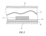
- the conducting plate 20 may be made of an electrically conducting metal material, such as an aluminum alloy or a copper foil.
- the conducting plate 20 and the necessary wires and pins carried thereon may be integrated using a metal core printed circuit board (MCPCB) by passing through a reflow oven once only.
- MCPCB metal core printed circuit board
- the conducting plate 20 supports the solar cell chip 21 thereon, and carries wires and pins (not shown) necessary for the solar cell chip packaging structure, and the solar cell chip 21 is electrically connected to the pins.
- the conducting plate 20 may be made of an electrically conducting metal material, such as an aluminum alloy or a copper foil.
- the conducting plate 20 and the necessary wires and pins carried thereon may be integrated using a metal core printed circuit board (MCPCB) by passing through a reflow oven once only.
- MCPCB metal core printed circuit board
Landscapes
- Physics & Mathematics (AREA)
- Condensed Matter Physics & Semiconductors (AREA)
- Electromagnetism (AREA)
- General Physics & Mathematics (AREA)
- Engineering & Computer Science (AREA)
- Computer Hardware Design (AREA)
- Microelectronics & Electronic Packaging (AREA)
- Power Engineering (AREA)
- Photovoltaic Devices (AREA)
Priority Applications (1)
| Application Number | Priority Date | Filing Date | Title |
|---|---|---|---|
| EP07150410A EP2073281A1 (de) | 2007-12-21 | 2007-12-21 | Konzentrator-Solarzellenchip-Verpackungsstruktur und Herstellungsverfahren dafür |
Applications Claiming Priority (1)
| Application Number | Priority Date | Filing Date | Title |
|---|---|---|---|
| EP07150410A EP2073281A1 (de) | 2007-12-21 | 2007-12-21 | Konzentrator-Solarzellenchip-Verpackungsstruktur und Herstellungsverfahren dafür |
Publications (1)
| Publication Number | Publication Date |
|---|---|
| EP2073281A1 true EP2073281A1 (de) | 2009-06-24 |
Family
ID=39410380
Family Applications (1)
| Application Number | Title | Priority Date | Filing Date |
|---|---|---|---|
| EP07150410A Withdrawn EP2073281A1 (de) | 2007-12-21 | 2007-12-21 | Konzentrator-Solarzellenchip-Verpackungsstruktur und Herstellungsverfahren dafür |
Country Status (1)
| Country | Link |
|---|---|
| EP (1) | EP2073281A1 (de) |
Citations (3)
| Publication number | Priority date | Publication date | Assignee | Title |
|---|---|---|---|---|
| US4834805A (en) * | 1987-09-24 | 1989-05-30 | Wattsun, Inc. | Photovoltaic power modules and methods for making same |
| US20060137733A1 (en) * | 2002-05-17 | 2006-06-29 | Schripsema Jason E | Photovoltaic module with adjustable heat sink and method of fabrication |
| US20070272295A1 (en) * | 2006-05-26 | 2007-11-29 | Rubin Leonid B | Heat sink for photovoltaic cells |
-
2007
- 2007-12-21 EP EP07150410A patent/EP2073281A1/de not_active Withdrawn
Patent Citations (3)
| Publication number | Priority date | Publication date | Assignee | Title |
|---|---|---|---|---|
| US4834805A (en) * | 1987-09-24 | 1989-05-30 | Wattsun, Inc. | Photovoltaic power modules and methods for making same |
| US20060137733A1 (en) * | 2002-05-17 | 2006-06-29 | Schripsema Jason E | Photovoltaic module with adjustable heat sink and method of fabrication |
| US20070272295A1 (en) * | 2006-05-26 | 2007-11-29 | Rubin Leonid B | Heat sink for photovoltaic cells |
Similar Documents
| Publication | Publication Date | Title |
|---|---|---|
| TWI576861B (zh) | 導電鋁膠及其製造方法、太陽能電池及其模組 | |
| US20080121269A1 (en) | Photovoltaic micro-concentrator modules | |
| JP2008205137A (ja) | 太陽電池及び太陽電池モジュール | |
| CN106910691B (zh) | 功率变流器中igbt模块的散热结构及封装工艺 | |
| EP2442370A2 (de) | Verpackungsstruktur für eine konzentrierte Photovoltaikzelle | |
| WO2009107804A1 (ja) | 太陽電池モジュール | |
| JP2008205045A (ja) | 太陽電池モジュールの製造方法 | |
| KR101232034B1 (ko) | 방열패키지 일체형 태양전지모듈 | |
| CN104868007A (zh) | 聚光型光电转换装置及其制造方法 | |
| US20100224250A1 (en) | Solar cell device structure | |
| JP2008300823A (ja) | 集光型太陽光電池モジュール | |
| US20090159127A1 (en) | Concentration solar cell chip packaging structure and method of forming the same | |
| US20160043249A1 (en) | Solar cell module and method of fabricating the same | |
| EP2073281A1 (de) | Konzentrator-Solarzellenchip-Verpackungsstruktur und Herstellungsverfahren dafür | |
| JP2010050442A (ja) | 太陽電池とその製造方法 | |
| CN102110762A (zh) | 一种集散热板与电极于一体的散热器件及其制备方法 | |
| WO2014037722A1 (en) | Concentrated photovoltaic (cpv) cell module with secondary optical element and method of fabrication | |
| WO2014037721A1 (en) | Concentrated photovoltaic (cpv) cell arrangement, module and method of fabrication | |
| KR101306411B1 (ko) | 태양전지 모듈 | |
| US8778704B1 (en) | Solar powered IC chip | |
| JP2002170975A (ja) | 半導体素子搭載用基板及び該基板を使用した半導体デバイス | |
| TWM469619U (zh) | 太陽能電池模組 | |
| CN220172139U (zh) | 一种高耐候型太阳能电池组件用薄膜 | |
| CN216671677U (zh) | 一种led芯片封装结构 | |
| KR101305682B1 (ko) | 태양광 발전 장치 및 이의 제조 방법 |
Legal Events
| Date | Code | Title | Description |
|---|---|---|---|
| PUAI | Public reference made under article 153(3) epc to a published international application that has entered the european phase |
Free format text: ORIGINAL CODE: 0009012 |
|
| AK | Designated contracting states |
Kind code of ref document: A1 Designated state(s): AT BE BG CH CY CZ DE DK EE ES FI FR GB GR HU IE IS IT LI LT LU LV MC MT NL PL PT RO SE SI SK TR |
|
| AX | Request for extension of the european patent |
Extension state: AL BA HR MK RS |
|
| AKX | Designation fees paid | ||
| STAA | Information on the status of an ep patent application or granted ep patent |
Free format text: STATUS: THE APPLICATION IS DEEMED TO BE WITHDRAWN |
|
| 18D | Application deemed to be withdrawn |
Effective date: 20091229 |
|
| REG | Reference to a national code |
Ref country code: DE Ref legal event code: 8566 |