EP2071721A1 - Piezoelectric resonator in a small-sized package - Google Patents
Piezoelectric resonator in a small-sized package Download PDFInfo
- Publication number
- EP2071721A1 EP2071721A1 EP07123177A EP07123177A EP2071721A1 EP 2071721 A1 EP2071721 A1 EP 2071721A1 EP 07123177 A EP07123177 A EP 07123177A EP 07123177 A EP07123177 A EP 07123177A EP 2071721 A1 EP2071721 A1 EP 2071721A1
- Authority
- EP
- European Patent Office
- Prior art keywords
- piezoelectric resonator
- lid
- vibrating arms
- attachment arm
- resonator according
- Prior art date
- Legal status (The legal status is an assumption and is not a legal conclusion. Google has not performed a legal analysis and makes no representation as to the accuracy of the status listed.)
- Granted
Links
Images

Classifications
-
- H—ELECTRICITY
- H03—ELECTRONIC CIRCUITRY
- H03H—IMPEDANCE NETWORKS, e.g. RESONANT CIRCUITS; RESONATORS
- H03H9/00—Networks comprising electromechanical or electro-acoustic elements; Electromechanical resonators
- H03H9/15—Constructional features of resonators consisting of piezoelectric or electrostrictive material
- H03H9/21—Crystal tuning forks
-
- H—ELECTRICITY
- H03—ELECTRONIC CIRCUITRY
- H03H—IMPEDANCE NETWORKS, e.g. RESONANT CIRCUITS; RESONATORS
- H03H9/00—Networks comprising electromechanical or electro-acoustic elements; Electromechanical resonators
- H03H9/02—Details
- H03H9/05—Holders or supports
- H03H9/10—Mounting in enclosures
- H03H9/1007—Mounting in enclosures for bulk acoustic wave [BAW] devices
- H03H9/1014—Mounting in enclosures for bulk acoustic wave [BAW] devices the enclosure being defined by a frame built on a substrate and a cap, the frame having no mechanical contact with the BAW device
- H03H9/1021—Mounting in enclosures for bulk acoustic wave [BAW] devices the enclosure being defined by a frame built on a substrate and a cap, the frame having no mechanical contact with the BAW device the BAW device being of the cantilever type
Definitions
- the present invention concerns packaged piezoelectric resonators or, in other words, devices formed each by a piezoelectric resonator and the case in which it is housed.
- the present invention more particularly concerns packaged piezoelectric resonators of small dimensions which are most often used for making frequency generators in particular for portable electronic equipment, in numerous fields such as horology, information technology, telecommunications and the medical field.
- Resonator 10 represented on Figure 1 , is intended to be mounted in a package. It includes a tuning fork shaped part with two parallel arms 12, 14 connected to each other by a linking part 16 and carrying electrodes 20, 22 to make them vibrate, these electrodes being connected to connecting pads 28, 30 intended to be electrically connected to the exterior of the case.
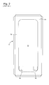
- Figure 2 is a top view of a known package (shown with its lid off) for receiving a piezoelectric resonator of the type corresponding to the field of the invention. It is understood that the size of the package depends on the general shape of the resonator, which may vary according to the embodiment considered.
- Package 70 of parallelepiped shape includes a case formed by a flat bottom 72 and four sides 74, and a lid (not shown).
- Two conductive elements, such as thin conductive layers, studs or bumps 78 and 80, are arranged on the flat bottom 72 for contacting the connecting pads 28, 30 of the resonator 10 ( Figure 1 ).
- the lid can be fastened on by vacuum soldering its edges onto the sides 74 of the case. This can be done by heating and pressure, by means of a soldering frame (not shown).
- the flat bottom 72 and the four sides 74 of the case of Figure 2 can be formed by etching layers of ceramic. If the lid for the case is not made of ceramic like the rest of the package, it can be made for example from metal, glass or silicon.
- Prior patent document US 7,084,556 partly solves the above problem by providing an improved tuning fork resonator including an additional central attachment arm 18 ( Figure 1 ) connected to linking part 16 and located between arms 12, 14 of the tuning fork shaped part, substantially equidistant from them.
- a base part 62 can further be formed at the end of the attachment arm opposite the linking part 16.
- the base part extends beyond vibrating arms 12 and 14 and preferably carries the connecting pads 28, 30 of the resonator.
- the resonator 10 is mounted in its case by bonding the base part 62 and/or the attachment arm 18, through at least one attachment point, to the bottom of the case.
- the base part is preferably used both for bonding resonator 10 to the inside its packaging, and for electrically connecting electrodes 20, 22 to conductive elements inside the packaging (not shown).
- One aim of the invention is to limit the sagging of the lid so that sufficient clearance is maintained between the vibrating arms and the underside of the lid.
- the invention concerns a packaged piezoelectric resonator according to the appended claim 1.
- the inside surface of the lid is stepped and comprises a portion of substantially greater thickness extending over the attachment arm. Therefore, any significant sagging of the lid causes this thicker portion of the lid it to come to rest on the attachment arm. Any further sagging of the lid is thus prevented. Further, the portion of the lid extending over the distal end portions of the vibrating arms is of lesser thickness. This insures that the clearance remains sufficient to avoid any risk of the vibrating arms colliding with the underside of the lid.
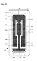
- the resonator according to the invention designated by the reference numeral 110, includes a tuning fork shaped part with two vibrating arms 112 and 114 joined by a linking part 116 to which a central attachment arm 118, located between arms 112 and 114 and parallel thereto, is connected.
- the whole assembly is made from a single piece of quartz.
- the central arm 118 is slightly longer than the vibrating arms 112 and 114.
- the distal end of the central arm widens into a base part 162 extending beyond the vibrating arms.
- the base part 162 is used both for fixing resonator 110 to the bottom of its packaging and for electrically connecting the driving electrodes (not shown) of the resonator to conductive studs or bumps 178 and 180 formed inside the packaging.
- each of the vibrating arms 112 and 114 widens into a flipper (166 and 168 respectively) which is almost twice as wide as the rest of the vibrating arm.
- the rectangular shaped flippers are preferably not arranged symmetrically with respect to the longitudinal axis of the vibrating arms. Rather, as shown in Figure 3a , the flippers 166, 168 can be offset towards the central arm 118.
- the central arm comprises a narrowed portion 176. As shown in Figure 3a , the narrowed portion 176 extends between the flippers 166 and 168.
- the attachment arm 118 is positioned on top of fixing stud or bump 182 formed on the flat bottom of the package 170.
- resonator 110 is also fixed to conductive studs 178 and 180.
- studs 178, 180 and 182 form a tripod mounting for fixing the resonator 110 inside the package 170. This tripod mounting also provides sufficient clearance between the vibrating arms and the flat bottom 172.
- the attachment arm 118 and the base part 162 may for example be glued or welded to the three studs.
- the portion of the attachment arm 118 lying between fixing stud 182 and linking part 116 is preferably at least one and a half times as wide as one of the vibrating arms.
- decoupling means 150 are arranged on the central arm near linking part 116. These decoupling means are provided in order to mechanically decouple central attachment arm 118 from vibrating arms 112 and 114. As shown, the decoupling means may be implemented in the form of notches 150 on either side of central arm 118.
- the decoupling means are arranged between fixing stud 182 and linking part 116. Preferably nearer linking part 116.
- vibrating arms 112 and 114 carry two groups of electrodes (not shown), which can be arranged and connected to each other in a similar fashion as the electrode groups 20 and 22 shown in figure 1 .
- the two electrode groups are further connected to two conductive connection pads (not shown) formed on the back of base part 162. These connection pads are arranged to make contact with conducting studs 178 and 180 respectively.
- At least one groove can further be formed on at least one of the front or rear side of each vibrating arm.
- the presence of grooves allows producing an excitation electrical field which is more homogeneous and locally more intense and for which vibration loss at the arms is low even when the size of the vibrating piece is miniaturized.
- the piezoelectric resonator 110 shown in Figures 3a and 3b is fixedly mounted in package 170.
- the actual size of the package is preferably chosen according the size and general shape of the resonator, which may vary according to the embodiment considered.
- Package 170 of parallelepiped shape includes a case formed by a flat bottom 172 and four sides 174, and a lid 140 (shown in Figure 3b ).
- the lid has an edge via which it is vacuum soldered, on sides 174 of the main part, by heating and pressure, by means of a soldering frame (not shown), after the resonator has been mounted in case 170.
- the height of the three studs 178, 180 and 182 supporting the resonator 110 is chosen so that the vibrating arms of the resonator may vibrate freely inside case 170.
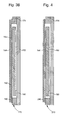
- FIG. 3b shows the packaged resonator of figure 3a with its top or lid 140 on.
- the lid is not of uniform thickness.
- a first portion of the lid has a first thickness, while the rest of the lid has a second thickness, which is substantially greater than the first thickness.
- the portion of the lid having the first thickness forms a large recessed area 142 on the inside of the lid.
- the purpose of using a lid comprising portions of different thickness is to reconcile the contradictory requirements of providing sufficient clearance above the vibrating arms, and of reducing the overall height of package 170.
- the recessed portion 142 can be formed by removing some of the material of the lid by etching, chemical etching, Deep reactive lon Etching, or even by drop forging in the case of a lid made of metal.
- the recessed portion 142 covers practically the entire area facing the flat bottom 172, except for a bulging portion or protrusion 144. It should be understood however that, according to alternative embodiments, instead of extending over the entire area facing the flat bottom 172, the recessed portion 142 could be limited to the area directly facing the vibrating arms 112 and 114, or even limited to the area directly facing the distal end portions of these vibrating arms.
- the above mentioned bulging portion or protrusion 144 extends on the inside of the lid 140 in a location facing the central arm 118.
- the protrusion 144 is arranged so as to be located directly across from the attachment point where central arm 118 is attached to fixing stud 182.
- the inside of the package depicted in Figure 3a and 3b is intended to be maintained under vacuum conditions.
- the atmospheric pressure on the outside of the lid 140 can cause it to sag substantially.
- this problem is cured by providing a bulging portion or a protrusion 144 extending downwards from the inside surface of the lid.
- this bulging portion comes to rest on top of the central arm 118.
- the lid thus being supported by the central arm, it is prevented from sagging any further.
- the distal end portions of the vibrating arms are positioned across from the recessed portion 142, the clearance between the vibrating arms and the lid stays sufficient to ensure that no collision occurs.
- FIG 4 shows still another embodiment of the packaged resonator according to the present invention.
- lid 240 does not comprise a recessed area. Rather, the entire lid has a reduced thickness (except for the protrusion 144).
- the sides 274 of the package are made slightly higher than the sides 174 of the package shown in Figure 3 .
Landscapes
- Physics & Mathematics (AREA)
- Acoustics & Sound (AREA)
- Chemical & Material Sciences (AREA)
- Crystallography & Structural Chemistry (AREA)
- Piezo-Electric Or Mechanical Vibrators, Or Delay Or Filter Circuits (AREA)
Abstract

Description
- The present invention concerns packaged piezoelectric resonators or, in other words, devices formed each by a piezoelectric resonator and the case in which it is housed. The present invention more particularly concerns packaged piezoelectric resonators of small dimensions which are most often used for making frequency generators in particular for portable electronic equipment, in numerous fields such as horology, information technology, telecommunications and the medical field.
- Such a packaged resonator of small dimensions has been disclosed in the prior art document
US 7,084,556 filed in the name of the Assignee, and which is incorporated herewith by way of reference.Resonator 10, represented onFigure 1 , is intended to be mounted in a package. It includes a tuning fork shaped part with twoparallel arms part 16 and carryingelectrodes pads -
Figure 2 is a top view of a known package (shown with its lid off) for receiving a piezoelectric resonator of the type corresponding to the field of the invention. It is understood that the size of the package depends on the general shape of the resonator, which may vary according to the embodiment considered.Package 70 of parallelepiped shape includes a case formed by aflat bottom 72 and foursides 74, and a lid (not shown). Two conductive elements, such as thin conductive layers, studs orbumps flat bottom 72 for contacting the connectingpads Figure 1 ). After theresonator 10 has been mounted in thecase 70, the lid can be fastened on by vacuum soldering its edges onto thesides 74 of the case. This can be done by heating and pressure, by means of a soldering frame (not shown). In a known manner, theflat bottom 72 and the foursides 74 of the case ofFigure 2 can be formed by etching layers of ceramic. If the lid for the case is not made of ceramic like the rest of the package, it can be made for example from metal, glass or silicon. - One of the problems with most conventional resonators is that they are designed to be bonded to a support substrate at one of their ends only. With such a design, it is difficult to guarantee that the planar tuning-fork-shaped part of the resonator is properly positioned and aligned parallel to the surface of the support substrate. In case of misalignment, there is a risk that the vibrating arms of the resonator will collide with the surface of the support substrate or with the lid of the package. In order to prevent such an outcome, sufficient clearance must be provided above and below the resonator. This requirement for clearance severely limits the possibility of designing ever thinner and more compact packaged piezoelectric resonators.
- Prior patent document
US 7,084,556 partly solves the above problem by providing an improved tuning fork resonator including an additional central attachment arm 18 (Figure 1 ) connected to linkingpart 16 and located betweenarms Figure 1 , abase part 62 can further be formed at the end of the attachment arm opposite the linkingpart 16. According to the depicted example, the base part extends beyond vibratingarms pads resonator 10 is mounted in its case by bonding thebase part 62 and/or theattachment arm 18, through at least one attachment point, to the bottom of the case. The base part is preferably used both for bondingresonator 10 to the inside its packaging, and for electrically connectingelectrodes - The provision for a resonator with at least one attachment arm disclosed by patent document
US 7,084,556 amounts to a considerable improvement. However, a need subsists for an even slimmer and more compact packaged piezoelectric resonator. Therefore, one aim of the present invention is to further improve the slimness and the compactness of packaged piezoelectric resonators. - One way of achieving this result is to reduce the thickness of the lid of the package housing the piezoelectric resonator. However, the inside of the package is usually maintained under vacuum conditions. Therefore, the lid is submitted to considerable pressure exerted by the atmosphere on the outside of the package. In many cases, the atmospheric pressure will be enough to cause the lid to sag substantially. As the clearance between the vibrating arms and the lid should be minimal, this sagging of the lid can cause collisions between the vibrating arms and the underside of the lid.
- One aim of the invention is to limit the sagging of the lid so that sufficient clearance is maintained between the vibrating arms and the underside of the lid.
- For this purpose, the invention concerns a packaged piezoelectric resonator according to the appended claim 1.
- One will understand that, according to the present invention, the inside surface of the lid is stepped and comprises a portion of substantially greater thickness extending over the attachment arm. Therefore, any significant sagging of the lid causes this thicker portion of the lid it to come to rest on the attachment arm. Any further sagging of the lid is thus prevented. Further, the portion of the lid extending over the distal end portions of the vibrating arms is of lesser thickness. This insures that the clearance remains sufficient to avoid any risk of the vibrating arms colliding with the underside of the lid.
- Other features and advantages of the invention will appear upon reading the following description which refers to the annexed drawings in which:
-
Figure 1 is a prior art example of a piezoelectric resonator of the type corresponding to the field of the present invention; -
Figure 2 is a top view of a suitable package for receiving a piezoelectric resonator of the type shown infigure 1 ; -
Figures 3a is a top view of a piezoelectric resonator mounted in a package according to a particular embodiment of the present invention; -
Figure 3b is a side view of the packaged resonator offigure 3a ; -
Figure 4 is a side view of a packaged resonator corresponding to an alternative embodiment of the present invention. - In the embodiment shown in relation with
Figures 3a , and3b , the resonator according to the invention, designated by thereference numeral 110, includes a tuning fork shaped part with two vibratingarms part 116 to which acentral attachment arm 118, located betweenarms - As visible in
Figure 3a , thecentral arm 118 is slightly longer than the vibratingarms base part 162 extending beyond the vibrating arms. Thebase part 162 is used both forfixing resonator 110 to the bottom of its packaging and for electrically connecting the driving electrodes (not shown) of the resonator to conductive studs orbumps - The distal end of each of the vibrating
arms Figure 3a , theflippers central arm 118. In this case, in order to provide sufficient lateral clearance between theflippers central arm 118, the central arm comprises a narrowedportion 176. As shown inFigure 3a , thenarrowed portion 176 extends between theflippers - As can be seen in
Figures 3a and3b , theattachment arm 118 is positioned on top of fixing stud orbump 182 formed on the flat bottom of thepackage 170. As previously mentioned,resonator 110 is also fixed toconductive studs studs resonator 110 inside thepackage 170. This tripod mounting also provides sufficient clearance between the vibrating arms and theflat bottom 172. Theattachment arm 118 and thebase part 162 may for example be glued or welded to the three studs. As visible inFigure 3a , the portion of theattachment arm 118 lying between fixingstud 182 and linkingpart 116 is preferably at least one and a half times as wide as one of the vibrating arms. Further, in the present embodiment, decoupling means 150 are arranged on the central arm near linkingpart 116. These decoupling means are provided in order to mechanically decouplecentral attachment arm 118 from vibratingarms notches 150 on either side ofcentral arm 118. The decoupling means are arranged between fixingstud 182 and linkingpart 116. Preferably nearer linkingpart 116. - As is usual with this type of resonator, vibrating
arms electrode groups figure 1 . The two electrode groups are further connected to two conductive connection pads (not shown) formed on the back ofbase part 162. These connection pads are arranged to make contact with conductingstuds - As known from the prior art, in order to reduce the amount of energy consumed by the resonator, at least one groove (not shown) can further be formed on at least one of the front or rear side of each vibrating arm. The presence of grooves allows producing an excitation electrical field which is more homogeneous and locally more intense and for which vibration loss at the arms is low even when the size of the vibrating piece is miniaturized.
- As previously mentioned, the
piezoelectric resonator 110 shown inFigures 3a and3b is fixedly mounted inpackage 170. The actual size of the package is preferably chosen according the size and general shape of the resonator, which may vary according to the embodiment considered. Package 170 of parallelepiped shape includes a case formed by aflat bottom 172 and foursides 174, and a lid 140 (shown inFigure 3b ). The lid has an edge via which it is vacuum soldered, onsides 174 of the main part, by heating and pressure, by means of a soldering frame (not shown), after the resonator has been mounted incase 170. The height of the threestuds resonator 110 is chosen so that the vibrating arms of the resonator may vibrate freely insidecase 170. - The side view of
Figure 3b shows the packaged resonator offigure 3a with its top orlid 140 on. As can be seen, the lid is not of uniform thickness. A first portion of the lid has a first thickness, while the rest of the lid has a second thickness, which is substantially greater than the first thickness. The portion of the lid having the first thickness forms a large recessedarea 142 on the inside of the lid. The purpose of using a lid comprising portions of different thickness is to reconcile the contradictory requirements of providing sufficient clearance above the vibrating arms, and of reducing the overall height ofpackage 170. In the case of a lid made of glass, of silicon, or of metal, the recessedportion 142 can be formed by removing some of the material of the lid by etching, chemical etching, Deep reactive lon Etching, or even by drop forging in the case of a lid made of metal. - As shown in
Figure 3b , according to the present embodiment, the recessedportion 142 covers practically the entire area facing theflat bottom 172, except for a bulging portion orprotrusion 144. It should be understood however that, according to alternative embodiments, instead of extending over the entire area facing theflat bottom 172, the recessedportion 142 could be limited to the area directly facing the vibratingarms - As shown in
Figure 3a , the above mentioned bulging portion orprotrusion 144 extends on the inside of thelid 140 in a location facing thecentral arm 118. Preferably, theprotrusion 144 is arranged so as to be located directly across from the attachment point wherecentral arm 118 is attached to fixingstud 182. - The inside of the package depicted in
Figure 3a and3b is intended to be maintained under vacuum conditions. When thelid 140 is made thin in order to produce a slimmer package, the atmospheric pressure on the outside of thelid 140 can cause it to sag substantially. According to the present invention, this problem is cured by providing a bulging portion or aprotrusion 144 extending downwards from the inside surface of the lid. When the lid sags, this bulging portion comes to rest on top of thecentral arm 118. The lid thus being supported by the central arm, it is prevented from sagging any further. As the distal end portions of the vibrating arms are positioned across from the recessedportion 142, the clearance between the vibrating arms and the lid stays sufficient to ensure that no collision occurs. -
Figure 4 shows still another embodiment of the packaged resonator according to the present invention. According to this particular embodiment,lid 240 does not comprise a recessed area. Rather, the entire lid has a reduced thickness (except for the protrusion 144). According to this embodiment, in order to provide sufficient clearance for the vibrating arms, thesides 274 of the package are made slightly higher than thesides 174 of the package shown inFigure 3 . - Having described the invention with regard to certain specific embodiments, it is to be understood that these embodiments are not meant as limitations of the invention. Indeed, various modifications, adaptations and/or combination between embodiments may become apparent to those skilled in the art without departing from the scope of the annexed claims. In particular, patent document
US 7,084,556 describes ten different packaged resonators of the type corresponding to the field of the present invention. The present invention could be routinely implemented with any of these different packaged resonators.
Claims (11)
- A packaged piezoelectric resonator comprising:a case (170; 270) with a lid (140; 240) and a piezoelectric resonator element (110) housed in said case, the piezoelectric resonator element including:characterized in that the inside surface of the lid (140, 240) is stepped in such a way as to form a first portion (142) where the lid has a first thickness and a second portion (144) where the lid has a second thickness substantially greater than the first thickness, the first portion (142) extending at least over distal end portions (166, 168) of the vibrating arms (112, 114), and the second portion (144) extending at least over a part of the attachment arm (118).a planar tuning-fork-shaped part with two parallel vibrating arms (112, 114) connected to each other by a linking part (116); andan attachment arm (118) extending from said linking part along the plane of said planar tuning-fork-shaped part, said attachment arm (118) being fixedly attached to the bottom (172) of said case (170) through at least one attachment point (178, 180, 182), and at least a main portion (118) of said attachment arm being arranged parallel and side by side with said vibrating arms,
- The packaged piezoelectric resonator according to claim 1, wherein said attachment arm (118) is located in between said vibrating arms (112, 114).
- The packaged piezoelectric resonator according to claim 2, wherein said attachment arm (118) is fixedly attached to the bottom (172) of said case (170) through a central attachment point (182) located between said vibrating arms (112, 114).
- The packaged piezoelectric resonator according to claim 2, wherein a distal end of the attachment arm (118) widens into a base part (162) opposite the linking part (116) and extending beyond the vibrating arms (112, 114), said base part being fixedly attached to the bottom (172).
- The packaged piezoelectric resonator according to claim 4, wherein said base part (162) comprises two distal attachment points (178, 180) with the bottom (172) of said case (170), and wherein said two distal attachment points form, together with a central attachment point (182) located between said vibrating arms (112, 114), a tripod mounting for said resonator (110).
- The packaged piezoelectric resonator according to any one of the preceding claims, wherein the said first portion (142) covers substantially the entire area facing the bottom (172), except for a bulging portion or protrusion (144) facing a part of the attachment arm (118).
- The packaged piezoelectric resonator according to claim 6, wherein said protrusion (144) faces said central attachment point (182).
- The packaged piezoelectric resonator according to anyone of claims 1 to 5, wherein said first portion (142) forms two recesses in the inside portion of the lid, said recesses each facing one of said vibrating arms (112) and (114).
- The packaged piezoelectric resonator according to claim 8, wherein said recesses (142) each directly face the distal end of one of the vibrating arms (112, 114).
- The packaged piezoelectric resonator according to any one of the claims 3, 5 , 6, 7, 8, 9, wherein the attachment arm (118) comprises decoupling means (150), said decoupling means being arranged between said central attachment point (182) and said linking part (116).
- The packaged piezoelectric resonator according to claim 10, wherein said decoupling means are formed by notches (150) on either side of the attachment arm (118)
Priority Applications (9)
| Application Number | Priority Date | Filing Date | Title |
|---|---|---|---|
| DE602007012732T DE602007012732D1 (en) | 2007-12-13 | 2007-12-13 | Piezoelectric resonator in a small package |
| EP07123177A EP2071721B1 (en) | 2007-12-13 | 2007-12-13 | Piezoelectric resonator in a small-sized package |
| AT07123177T ATE499746T1 (en) | 2007-12-13 | 2007-12-13 | PIEZOELECTRIC RESONATOR IN A SMALL PACKAGING |
| TW097148230A TWI395401B (en) | 2007-12-13 | 2008-12-11 | Piezoelectric resonator in a small-sized package |
| JP2008315307A JP5236445B2 (en) | 2007-12-13 | 2008-12-11 | Piezoelectric resonator housed in a small package |
| TW101113765A TWI488434B (en) | 2007-12-13 | 2008-12-11 | Piezoelectric resonator in a small-sized package |
| CN200810189564.9A CN101488734B (en) | 2007-12-13 | 2008-12-12 | Piezoelectric resonators in small packages |
| CN201210083740.7A CN102723926B (en) | 2007-12-13 | 2008-12-12 | The piezo-electric resonator of small-sized package |
| JP2012035848A JP5279924B2 (en) | 2007-12-13 | 2012-02-22 | Piezoelectric resonator housed in a small package |
Applications Claiming Priority (1)
| Application Number | Priority Date | Filing Date | Title |
|---|---|---|---|
| EP07123177A EP2071721B1 (en) | 2007-12-13 | 2007-12-13 | Piezoelectric resonator in a small-sized package |
Publications (2)
| Publication Number | Publication Date |
|---|---|
| EP2071721A1 true EP2071721A1 (en) | 2009-06-17 |
| EP2071721B1 EP2071721B1 (en) | 2011-02-23 |
Family
ID=39387276
Family Applications (1)
| Application Number | Title | Priority Date | Filing Date |
|---|---|---|---|
| EP07123177A Active EP2071721B1 (en) | 2007-12-13 | 2007-12-13 | Piezoelectric resonator in a small-sized package |
Country Status (6)
| Country | Link |
|---|---|
| EP (1) | EP2071721B1 (en) |
| JP (2) | JP5236445B2 (en) |
| CN (2) | CN102723926B (en) |
| AT (1) | ATE499746T1 (en) |
| DE (1) | DE602007012732D1 (en) |
| TW (2) | TWI488434B (en) |
Cited By (4)
| Publication number | Priority date | Publication date | Assignee | Title |
|---|---|---|---|---|
| US20130175903A1 (en) * | 2012-01-09 | 2013-07-11 | Micro Crystal Ag | Small-sized piezoelectric tuning-fork resonator |
| EP2256923A4 (en) * | 2008-03-18 | 2013-11-06 | Citizen Holdings Co Ltd | PIEZOELECTRIC DEVICE |
| US9354128B2 (en) | 2013-12-27 | 2016-05-31 | Seiko Epson Corporation | Resonator element, resonator, oscillator, electronic apparatus, sensor, and mobile object |
| US9705472B2 (en) | 2013-06-24 | 2017-07-11 | Seiko Epson Corporation | Resonator element, resonator, electronic device, electronic apparatus, and moving object |
Families Citing this family (5)
| Publication number | Priority date | Publication date | Assignee | Title |
|---|---|---|---|---|
| JP5479931B2 (en) * | 2010-02-03 | 2014-04-23 | エスアイアイ・クリスタルテクノロジー株式会社 | Piezoelectric vibrators, oscillators, electronic equipment and radio clocks |
| US8283988B2 (en) * | 2010-02-25 | 2012-10-09 | Seiko Epson Corporation | Resonator element, resonator, oscillator, and electronic device |
| JP6155617B2 (en) * | 2012-12-13 | 2017-07-05 | セイコーエプソン株式会社 | Electronic devices, electronic devices, and moving objects |
| GB2530186B (en) * | 2013-06-29 | 2020-09-30 | Intel Corp | Piezoresistive resonator with multi-gate transistor |
| US10812046B2 (en) * | 2018-02-07 | 2020-10-20 | Murata Manufacturing Co., Ltd. | Micromechanical resonator having reduced size |
Citations (2)
| Publication number | Priority date | Publication date | Assignee | Title |
|---|---|---|---|---|
| US20030067248A1 (en) * | 2001-10-09 | 2003-04-10 | Eta Sa Fabriques D'ebauches | Piezoelectric resonator and assembly comprising the same enclosed in a case |
| US7084556B1 (en) | 2005-06-09 | 2006-08-01 | Eta Sa Manufacture Horlogere Suisse | Small-sized piezoelectric resonator |
Family Cites Families (15)
| Publication number | Priority date | Publication date | Assignee | Title |
|---|---|---|---|---|
| JPS4998219A (en) * | 1973-01-22 | 1974-09-17 | ||
| JPS5085170U (en) * | 1973-12-10 | 1975-07-21 | ||
| JP3336921B2 (en) * | 1997-08-04 | 2002-10-21 | 株式会社村田製作所 | Piezoelectric resonance components |
| JP4547788B2 (en) * | 2000-03-15 | 2010-09-22 | セイコーエプソン株式会社 | Package structure of piezoelectric vibrator |
| JP2002141770A (en) * | 2000-11-01 | 2002-05-17 | Citizen Watch Co Ltd | Small-sized vibrator |
| JP2002171150A (en) * | 2000-11-30 | 2002-06-14 | Seiko Epson Corp | Package structure of piezoelectric device |
| JP3995918B2 (en) * | 2001-10-29 | 2007-10-24 | セイコーインスツル株式会社 | Surface mount type piezoelectric vibrator |
| TW512551B (en) * | 2001-11-23 | 2002-12-01 | Ind Tech Res Inst | A structure of tuning fork resonator and a driving method thereof |
| JP3951058B2 (en) * | 2003-08-19 | 2007-08-01 | セイコーエプソン株式会社 | Tuning fork type piezoelectric vibrating piece |
| JP3797355B2 (en) * | 2003-10-22 | 2006-07-19 | セイコーエプソン株式会社 | Method for manufacturing piezoelectric vibrator |
| EP1536559A1 (en) * | 2003-11-25 | 2005-06-01 | ETA SA Manufacture Horlogère Suisse | Electronic device has a resonator element in a hemetically closed case |
| EP1633042B1 (en) * | 2004-09-03 | 2010-05-05 | ETA SA Manufacture Horlogère Suisse | Quartz resonator of very small dimensions |
| ATE421799T1 (en) * | 2005-06-09 | 2009-02-15 | Eta Sa Mft Horlogere Suisse | COMPACT PIEZOELECTRIC RESONATOR |
| EP1732219B1 (en) * | 2005-06-09 | 2008-03-26 | ETA SA Manufacture Horlogère Suisse | Piezoelectric resonator and assembly comprising the same enclosed in a case |
| JP2007258917A (en) * | 2006-03-22 | 2007-10-04 | Epson Toyocom Corp | Piezoelectric device |
-
2007
- 2007-12-13 DE DE602007012732T patent/DE602007012732D1/en active Active
- 2007-12-13 AT AT07123177T patent/ATE499746T1/en not_active IP Right Cessation
- 2007-12-13 EP EP07123177A patent/EP2071721B1/en active Active
-
2008
- 2008-12-11 TW TW101113765A patent/TWI488434B/en active
- 2008-12-11 TW TW097148230A patent/TWI395401B/en active
- 2008-12-11 JP JP2008315307A patent/JP5236445B2/en active Active
- 2008-12-12 CN CN201210083740.7A patent/CN102723926B/en active Active
- 2008-12-12 CN CN200810189564.9A patent/CN101488734B/en active Active
-
2012
- 2012-02-22 JP JP2012035848A patent/JP5279924B2/en active Active
Patent Citations (2)
| Publication number | Priority date | Publication date | Assignee | Title |
|---|---|---|---|---|
| US20030067248A1 (en) * | 2001-10-09 | 2003-04-10 | Eta Sa Fabriques D'ebauches | Piezoelectric resonator and assembly comprising the same enclosed in a case |
| US7084556B1 (en) | 2005-06-09 | 2006-08-01 | Eta Sa Manufacture Horlogere Suisse | Small-sized piezoelectric resonator |
Cited By (6)
| Publication number | Priority date | Publication date | Assignee | Title |
|---|---|---|---|---|
| EP2256923A4 (en) * | 2008-03-18 | 2013-11-06 | Citizen Holdings Co Ltd | PIEZOELECTRIC DEVICE |
| US20130175903A1 (en) * | 2012-01-09 | 2013-07-11 | Micro Crystal Ag | Small-sized piezoelectric tuning-fork resonator |
| US8933614B2 (en) * | 2012-01-09 | 2015-01-13 | Micro Crystal Ag | Small-sized piezoelectric tuning-fork resonator |
| US9705472B2 (en) | 2013-06-24 | 2017-07-11 | Seiko Epson Corporation | Resonator element, resonator, electronic device, electronic apparatus, and moving object |
| US10659006B2 (en) | 2013-06-24 | 2020-05-19 | Seiko Epson Corporation | Resonator element, resonator, electronic device, electronic apparatus, and moving object |
| US9354128B2 (en) | 2013-12-27 | 2016-05-31 | Seiko Epson Corporation | Resonator element, resonator, oscillator, electronic apparatus, sensor, and mobile object |
Also Published As
| Publication number | Publication date |
|---|---|
| ATE499746T1 (en) | 2011-03-15 |
| CN101488734B (en) | 2014-07-02 |
| DE602007012732D1 (en) | 2011-04-07 |
| JP5279924B2 (en) | 2013-09-04 |
| CN102723926B (en) | 2015-12-16 |
| TW201242243A (en) | 2012-10-16 |
| JP2009147935A (en) | 2009-07-02 |
| JP5236445B2 (en) | 2013-07-17 |
| TWI488434B (en) | 2015-06-11 |
| CN102723926A (en) | 2012-10-10 |
| TWI395401B (en) | 2013-05-01 |
| EP2071721B1 (en) | 2011-02-23 |
| TW200947858A (en) | 2009-11-16 |
| JP2012135021A (en) | 2012-07-12 |
| CN101488734A (en) | 2009-07-22 |
Similar Documents
| Publication | Publication Date | Title |
|---|---|---|
| EP2071721B1 (en) | Piezoelectric resonator in a small-sized package | |
| US7939995B2 (en) | Piezoelectric resonator in a small-sized package | |
| KR100667608B1 (en) | Ultra thin piezoelectric resonator | |
| EP1732217B1 (en) | Small-sized piezoelectric resonator | |
| US6700313B2 (en) | Piezoelectric resonator and assembly comprising the same enclosed in a case | |
| EP1732220B1 (en) | Small-sized piezoelectric resonator | |
| US7084556B1 (en) | Small-sized piezoelectric resonator | |
| JP4548012B2 (en) | Piezoelectric vibration device | |
| EP1732219B1 (en) | Piezoelectric resonator and assembly comprising the same enclosed in a case | |
| JP4741385B2 (en) | Structure | |
| JP2002009576A (en) | Piezoelectric device and its package structure | |
| JP2002325024A (en) | Electronic component and method for forming substrate electrode thereof | |
| JP2011040981A (en) | Piezoelectric device | |
| US20060279176A1 (en) | Small-sized piezoelectric resonator | |
| US7138752B1 (en) | Small-sized piezoelectric resonator | |
| JP2012169890A (en) | Piezoelectric device | |
| EP1732218B1 (en) | Small-sized piezoelectric resonator | |
| JP2006311310A (en) | Piezoelectric vibrator | |
| JP2006197477A (en) | Piezoelectric device package and piezoelectric device using the same | |
| JP2007208537A (en) | Bonding structure of piezoelectric vibrating piece and piezoelectric device | |
| HK1098886B (en) | Small-sized piezoelectric resonator | |
| HK1098885B (en) | Small-sized piezoelectric resonator | |
| HK1055854B (en) | Piezoelectric resonator and assembly comprising the same enclosed in a case | |
| JP2004350016A (en) | Fixing structure of piezoelectric vibrating reed and piezoelectric device, mobile phone device using piezoelectric device, and electronic device using piezoelectric device | |
| JP2006339692A (en) | Piezoelectric vibrator |
Legal Events
| Date | Code | Title | Description |
|---|---|---|---|
| PUAI | Public reference made under article 153(3) epc to a published international application that has entered the european phase |
Free format text: ORIGINAL CODE: 0009012 |
|
| 17P | Request for examination filed |
Effective date: 20081211 |
|
| AK | Designated contracting states |
Kind code of ref document: A1 Designated state(s): AT BE BG CH CY CZ DE DK EE ES FI FR GB GR HU IE IS IT LI LT LU LV MC MT NL PL PT RO SE SI SK TR |
|
| AX | Request for extension of the european patent |
Extension state: AL BA HR MK RS |
|
| 17Q | First examination report despatched |
Effective date: 20090826 |
|
| AKX | Designation fees paid |
Designated state(s): AT BE BG CH CY CZ DE DK EE ES FI FR GB GR HU IE IS IT LI LT LU LV MC MT NL PL PT RO SE SI SK TR |
|
| GRAP | Despatch of communication of intention to grant a patent |
Free format text: ORIGINAL CODE: EPIDOSNIGR1 |
|
| GRAS | Grant fee paid |
Free format text: ORIGINAL CODE: EPIDOSNIGR3 |
|
| GRAA | (expected) grant |
Free format text: ORIGINAL CODE: 0009210 |
|
| AK | Designated contracting states |
Kind code of ref document: B1 Designated state(s): AT BE BG CH CY CZ DE DK EE ES FI FR GB GR HU IE IS IT LI LT LU LV MC MT NL PL PT RO SE SI SK TR |
|
| REG | Reference to a national code |
Ref country code: GB Ref legal event code: FG4D |
|
| REG | Reference to a national code |
Ref country code: CH Ref legal event code: NV Representative=s name: ICB INGENIEURS CONSEILS EN BREVETS SA Ref country code: CH Ref legal event code: EP |
|
| REG | Reference to a national code |
Ref country code: IE Ref legal event code: FG4D |
|
| REF | Corresponds to: |
Ref document number: 602007012732 Country of ref document: DE Date of ref document: 20110407 Kind code of ref document: P |
|
| REG | Reference to a national code |
Ref country code: DE Ref legal event code: R096 Ref document number: 602007012732 Country of ref document: DE Effective date: 20110407 |
|
| REG | Reference to a national code |
Ref country code: NL Ref legal event code: VDEP Effective date: 20110223 |
|
| LTIE | Lt: invalidation of european patent or patent extension |
Effective date: 20110223 |
|
| PG25 | Lapsed in a contracting state [announced via postgrant information from national office to epo] |
Ref country code: GR Free format text: LAPSE BECAUSE OF FAILURE TO SUBMIT A TRANSLATION OF THE DESCRIPTION OR TO PAY THE FEE WITHIN THE PRESCRIBED TIME-LIMIT Effective date: 20110524 Ref country code: SE Free format text: LAPSE BECAUSE OF FAILURE TO SUBMIT A TRANSLATION OF THE DESCRIPTION OR TO PAY THE FEE WITHIN THE PRESCRIBED TIME-LIMIT Effective date: 20110223 Ref country code: LT Free format text: LAPSE BECAUSE OF FAILURE TO SUBMIT A TRANSLATION OF THE DESCRIPTION OR TO PAY THE FEE WITHIN THE PRESCRIBED TIME-LIMIT Effective date: 20110223 Ref country code: ES Free format text: LAPSE BECAUSE OF FAILURE TO SUBMIT A TRANSLATION OF THE DESCRIPTION OR TO PAY THE FEE WITHIN THE PRESCRIBED TIME-LIMIT Effective date: 20110603 Ref country code: LV Free format text: LAPSE BECAUSE OF FAILURE TO SUBMIT A TRANSLATION OF THE DESCRIPTION OR TO PAY THE FEE WITHIN THE PRESCRIBED TIME-LIMIT Effective date: 20110223 Ref country code: PT Free format text: LAPSE BECAUSE OF FAILURE TO SUBMIT A TRANSLATION OF THE DESCRIPTION OR TO PAY THE FEE WITHIN THE PRESCRIBED TIME-LIMIT Effective date: 20110623 |
|
| PG25 | Lapsed in a contracting state [announced via postgrant information from national office to epo] |
Ref country code: BE Free format text: LAPSE BECAUSE OF FAILURE TO SUBMIT A TRANSLATION OF THE DESCRIPTION OR TO PAY THE FEE WITHIN THE PRESCRIBED TIME-LIMIT Effective date: 20110223 Ref country code: NL Free format text: LAPSE BECAUSE OF FAILURE TO SUBMIT A TRANSLATION OF THE DESCRIPTION OR TO PAY THE FEE WITHIN THE PRESCRIBED TIME-LIMIT Effective date: 20110223 Ref country code: SI Free format text: LAPSE BECAUSE OF FAILURE TO SUBMIT A TRANSLATION OF THE DESCRIPTION OR TO PAY THE FEE WITHIN THE PRESCRIBED TIME-LIMIT Effective date: 20110223 Ref country code: BG Free format text: LAPSE BECAUSE OF FAILURE TO SUBMIT A TRANSLATION OF THE DESCRIPTION OR TO PAY THE FEE WITHIN THE PRESCRIBED TIME-LIMIT Effective date: 20110523 Ref country code: CY Free format text: LAPSE BECAUSE OF FAILURE TO SUBMIT A TRANSLATION OF THE DESCRIPTION OR TO PAY THE FEE WITHIN THE PRESCRIBED TIME-LIMIT Effective date: 20110223 Ref country code: AT Free format text: LAPSE BECAUSE OF FAILURE TO SUBMIT A TRANSLATION OF THE DESCRIPTION OR TO PAY THE FEE WITHIN THE PRESCRIBED TIME-LIMIT Effective date: 20110223 Ref country code: FI Free format text: LAPSE BECAUSE OF FAILURE TO SUBMIT A TRANSLATION OF THE DESCRIPTION OR TO PAY THE FEE WITHIN THE PRESCRIBED TIME-LIMIT Effective date: 20110223 |
|
| PG25 | Lapsed in a contracting state [announced via postgrant information from national office to epo] |
Ref country code: EE Free format text: LAPSE BECAUSE OF FAILURE TO SUBMIT A TRANSLATION OF THE DESCRIPTION OR TO PAY THE FEE WITHIN THE PRESCRIBED TIME-LIMIT Effective date: 20110223 Ref country code: DK Free format text: LAPSE BECAUSE OF FAILURE TO SUBMIT A TRANSLATION OF THE DESCRIPTION OR TO PAY THE FEE WITHIN THE PRESCRIBED TIME-LIMIT Effective date: 20110223 |
|
| PG25 | Lapsed in a contracting state [announced via postgrant information from national office to epo] |
Ref country code: SK Free format text: LAPSE BECAUSE OF FAILURE TO SUBMIT A TRANSLATION OF THE DESCRIPTION OR TO PAY THE FEE WITHIN THE PRESCRIBED TIME-LIMIT Effective date: 20110223 Ref country code: RO Free format text: LAPSE BECAUSE OF FAILURE TO SUBMIT A TRANSLATION OF THE DESCRIPTION OR TO PAY THE FEE WITHIN THE PRESCRIBED TIME-LIMIT Effective date: 20110223 Ref country code: CZ Free format text: LAPSE BECAUSE OF FAILURE TO SUBMIT A TRANSLATION OF THE DESCRIPTION OR TO PAY THE FEE WITHIN THE PRESCRIBED TIME-LIMIT Effective date: 20110223 |
|
| PLBE | No opposition filed within time limit |
Free format text: ORIGINAL CODE: 0009261 |
|
| STAA | Information on the status of an ep patent application or granted ep patent |
Free format text: STATUS: NO OPPOSITION FILED WITHIN TIME LIMIT |
|
| 26N | No opposition filed |
Effective date: 20111124 |
|
| PG25 | Lapsed in a contracting state [announced via postgrant information from national office to epo] |
Ref country code: PL Free format text: LAPSE BECAUSE OF FAILURE TO SUBMIT A TRANSLATION OF THE DESCRIPTION OR TO PAY THE FEE WITHIN THE PRESCRIBED TIME-LIMIT Effective date: 20110223 |
|
| REG | Reference to a national code |
Ref country code: DE Ref legal event code: R097 Ref document number: 602007012732 Country of ref document: DE Effective date: 20111124 |
|
| PG25 | Lapsed in a contracting state [announced via postgrant information from national office to epo] |
Ref country code: IT Free format text: LAPSE BECAUSE OF FAILURE TO SUBMIT A TRANSLATION OF THE DESCRIPTION OR TO PAY THE FEE WITHIN THE PRESCRIBED TIME-LIMIT Effective date: 20110223 |
|
| PG25 | Lapsed in a contracting state [announced via postgrant information from national office to epo] |
Ref country code: MC Free format text: LAPSE BECAUSE OF NON-PAYMENT OF DUE FEES Effective date: 20111231 |
|
| REG | Reference to a national code |
Ref country code: IE Ref legal event code: MM4A |
|
| PG25 | Lapsed in a contracting state [announced via postgrant information from national office to epo] |
Ref country code: IE Free format text: LAPSE BECAUSE OF NON-PAYMENT OF DUE FEES Effective date: 20111213 |
|
| PG25 | Lapsed in a contracting state [announced via postgrant information from national office to epo] |
Ref country code: MT Free format text: LAPSE BECAUSE OF FAILURE TO SUBMIT A TRANSLATION OF THE DESCRIPTION OR TO PAY THE FEE WITHIN THE PRESCRIBED TIME-LIMIT Effective date: 20110223 |
|
| PG25 | Lapsed in a contracting state [announced via postgrant information from national office to epo] |
Ref country code: LU Free format text: LAPSE BECAUSE OF NON-PAYMENT OF DUE FEES Effective date: 20111213 |
|
| PG25 | Lapsed in a contracting state [announced via postgrant information from national office to epo] |
Ref country code: IS Free format text: LAPSE BECAUSE OF FAILURE TO SUBMIT A TRANSLATION OF THE DESCRIPTION OR TO PAY THE FEE WITHIN THE PRESCRIBED TIME-LIMIT Effective date: 20110223 |
|
| PG25 | Lapsed in a contracting state [announced via postgrant information from national office to epo] |
Ref country code: TR Free format text: LAPSE BECAUSE OF FAILURE TO SUBMIT A TRANSLATION OF THE DESCRIPTION OR TO PAY THE FEE WITHIN THE PRESCRIBED TIME-LIMIT Effective date: 20110223 |
|
| PG25 | Lapsed in a contracting state [announced via postgrant information from national office to epo] |
Ref country code: HU Free format text: LAPSE BECAUSE OF FAILURE TO SUBMIT A TRANSLATION OF THE DESCRIPTION OR TO PAY THE FEE WITHIN THE PRESCRIBED TIME-LIMIT Effective date: 20110223 |
|
| REG | Reference to a national code |
Ref country code: FR Ref legal event code: PLFP Year of fee payment: 9 |
|
| REG | Reference to a national code |
Ref country code: FR Ref legal event code: PLFP Year of fee payment: 10 |
|
| REG | Reference to a national code |
Ref country code: FR Ref legal event code: PLFP Year of fee payment: 11 |
|
| P01 | Opt-out of the competence of the unified patent court (upc) registered |
Effective date: 20230701 |
|
| REG | Reference to a national code |
Ref country code: CH Ref legal event code: U11 Free format text: ST27 STATUS EVENT CODE: U-0-0-U10-U11 (AS PROVIDED BY THE NATIONAL OFFICE) Effective date: 20260101 |
|
| PGFP | Annual fee paid to national office [announced via postgrant information from national office to epo] |
Ref country code: DE Payment date: 20251126 Year of fee payment: 19 |
|
| PGFP | Annual fee paid to national office [announced via postgrant information from national office to epo] |
Ref country code: GB Payment date: 20251120 Year of fee payment: 19 |
|
| PGFP | Annual fee paid to national office [announced via postgrant information from national office to epo] |
Ref country code: FR Payment date: 20251120 Year of fee payment: 19 |
|
| PGFP | Annual fee paid to national office [announced via postgrant information from national office to epo] |
Ref country code: CH Payment date: 20260101 Year of fee payment: 19 |